EP1586183B1 - Oscillator device for frequency modulation - Google Patents
Oscillator device for frequency modulation Download PDFInfo
- Publication number
- EP1586183B1 EP1586183B1 EP03782441A EP03782441A EP1586183B1 EP 1586183 B1 EP1586183 B1 EP 1586183B1 EP 03782441 A EP03782441 A EP 03782441A EP 03782441 A EP03782441 A EP 03782441A EP 1586183 B1 EP1586183 B1 EP 1586183B1
- Authority
- EP
- European Patent Office
- Prior art keywords
- oscillator
- current
- frequency
- input
- output
- Prior art date
- Legal status (The legal status is an assumption and is not a legal conclusion. Google has not performed a legal analysis and makes no representation as to the accuracy of the status listed.)
- Expired - Fee Related
Links
Images

Classifications
-
- H—ELECTRICITY
- H04—ELECTRIC COMMUNICATION TECHNIQUE
- H04L—TRANSMISSION OF DIGITAL INFORMATION, e.g. TELEGRAPHIC COMMUNICATION
- H04L27/00—Modulated-carrier systems
- H04L27/10—Frequency-modulated carrier systems, i.e. using frequency-shift keying
- H04L27/12—Modulator circuits; Transmitter circuits
Definitions
- the present invention relates to an oscillator arrangement designed for frequency modulation.
- Frequency Shift Keying in addition to amplitude shift keying and phase shift keying, as well as combinations of these methods, is a common method for digital modulation of a carrier signal.
- One way to apply a carrier to frequency shift keying is to modulate the carrier signal as it is being generated in the oscillator.
- the frequency shift keying of the oscillator is usually achieved by adding or disconnecting small, frequency-determining capacitances to a resonant circuit formed in the oscillator.
- the digital modulation signal is modulated onto the carrier with the desired frequency deviation.
- the oscillator can be embodied for example as a quartz oscillator or as an LC oscillator. While in a quartz oscillator, the oscillation frequency is mainly determined by the oscillation frequency of the quartz, at least one inductance and at least one capacitance influence the oscillation frequency in the case of the LC oscillator.
- the document US 2,874,216 relates to an automatic signal control system.
- the object of the present invention is to provide an oscillator arrangement which is suitable for a modulation according to a frequency shift keying method and in which problems caused by charge injection are avoided or significantly reduced.
- the automatic amplitude control which is usually present anyway in a controlled oscillator with frequency modulation, is also used to control the operating current of the oscillator and so that the oscillator frequency in the desired manner to influence, that is to modulate.
- the oscillator is thus modulated by the loop gain of the gain control loop is controlled by influencing the supply current of the oscillator.
- the amplitude control loop is used to change the so-called base current of the oscillator by means of the modulation signal controlled Stromabzugstechnik and thus to change the frequency in small steps.
- the proposed principle is advantageously applicable, inter alia, both in LC oscillators and quartz oscillators.
- the means for influencing the supply current preferably comprises a plurality of current switches connected in parallel with respect to their connected paths. Depending on the modulation signal, the parallel-connected current switches are preferably controlled so that just the current required for the desired frequency detuning current is subtracted.
- the parallel-connected current switches are preferably arranged on the output side in a current mirror.
- each one transistor of the current mirror and a switch associated therewith form a series circuit.
- the series circuits are connected in parallel to each other.
- the switches can be switched on and off independently of each other.
- the current mirror with the parallel-connected current switches preferably acts on a further current mirror, which couples a supply current source for supplying the oscillator with the oscillator.
- the circuit node at which the current mirror engages with the current switches in the supply current supply of the oscillator is preferably provided at the common gate terminal or base terminal of the current mirror transistors in the further current mirror.
- a control block is preferably provided with an input to which the modulation signal is supplied and with one or more outputs which are connected to respective control terminals of the associated power switch.
- the modulation signal is preferably a digitally coded signal, which is coded according to a frequency shift keying method, FSK.
- the oscillator is preferably designed to be tunable with a further control input, to which a tuning signal can be fed and with an oscillation frequency-determining capacitor, which is controlled in dependence on the tuning signal.
- Such tunable capacitances are preferably designed as varactor diodes.
- FIG. 1 shows an oscillator arrangement designed for frequency modulation. This comprises an oscillator 1 and a control input 2 for supplying a modulation signal.
- the oscillator 1 has an output 3 to which a frequency modulated signal can be tapped.
- the oscillator 1 has an input 4 for supplying a supply current.
- the supply current is used, inter alia, for the damping of the resonant circuit, which is formed in the oscillator 1.
- the supply current is also referred to as base current or tail current. To ensure the stability of the oscillator, this is arranged in an amplitude control loop.
- the control circuit for amplitude control comprises an AGC block 5, a first current mirror 6 and a second current mirror 7, 8.
- the output of the first current mirror 6 controls a Stromettintransistor 7, which at its current source output to the supply current input 4 of the oscillator. 1 connected is.
- a transistor diode 8 forms with the current source transistor 7, the second current mirror.
- the common gate terminal of the transistors 7, 8, which is connected to the output of the first current mirror 6, is referred to as circuit node K.
- the input of the second current mirror 7, 8 is connected to a current source 9, which provides a reference current for the oscillator 1.
- the current mirror 6 comprises a transistor diode M1 and the output side a total of four parallel-connected current mirror transistors M2, M3, M4, M5, which are independently switched on and off.
- a respective switch 10, 11, 12, 13 is provided, each of which connects a reference potential terminal 14 to a load terminal of the controlled paths of the associated transistor M2, M3, M4, M5, in this case with their source terminal.
- the gate terminals of the field effect transistors M1 to M5 in the current mirror 6 are connected directly to one another.
- the transistor M1 In order for the transistor M1 to operate as a diode, its gate terminal is directly connected to its drain terminal.
- the source terminal of the n-channel field effect transistor M1 is connected to the reference potential terminal 14.
- the drain terminals of the transistors M2 to M5 are directly connected together in the circuit node K and form the output of the current mirror 6.
- the circuit node K is connected directly to the gate terminals of the current mirror transistors 7, 8.
- the switches 10, 11, 12, 13, which are designed as a current switch, are controlled by a control logic which is provided in a corresponding control block 15, whose input forms the control input 2 for supplying a modulation signal of the oscillator arrangement and whose output to the control terminals of Switch 10, 11, 12, 13 is connected.
- a possibly existing tuning input of the voltage-controlled oscillator 1 is not shown in FIG.
- the peculiarity of the circuit according to FIG. 1 is that the modulation data does not control switchable capacitors provided directly in the oscillator core, which thus influence the oscillation frequency of the oscillator, but that the modulation data intervene in the amplitude regulation of the oscillator 1.
- the oscillator frequency is indirectly keyed over the control of the supply current of the oscillator, English tail current.
- the amplitude control circuit 5, 6, 7 comprises switchable current mirror, with which the frequency of the oscillator can be adjusted.
- the modulation signal thus controls the loop gain of the amplitude control loop 5, 6, 7.
- With the power switches frequency conversion of the oscillator 1 is realized in a Stromabzugstechnik.
- FIG. 2 shows a further exemplary embodiment of the present oscillator arrangement, which has an oscillator realized as quartz oscillator 1 '.
- the amplitude control including the switchable current sources in the amplitude control loop and their control with the modulation signal correspond to those of Figure 1.
- the oscillator 1 'in Figure 2 is designed as a quartz oscillator and comprises a quartz crystal 16. Both terminals of the quartz oscillator 16 are connected via a respective capacitor 17, 18 with reference potential.
- an amplifier is provided which comprises a p-channel field effect transistor 19.
- the gate terminal of the transistor 19, at the same time the output 3 of the oscillator is formed, is connected to one of the two terminals of the quartz 16.
- the source terminal of the transistor 19 is connected to reference potential.
- the drain terminal of the transistor 19, which forms the input for supplying a supply current 4 of the oscillator 1 ', is connected on the one hand via a resistor 20 to the gate terminal of the transistor 19 and connected to the other with the further terminal of the quartz 16.
- a frequency deviation is possible from 10 KHz to 100 KHz by appropriately switching the power switches 10, 11, 12, 13 in response to the modulation signal.
- the data rate can be between 0 and 20 kBit / sec.
- the time constant of the amplitude control of the amplitude control loop 5, 6, 7 should be set much smaller than the time constant of the oscillator.
- the frequency is changed via the current and, subsequently, via the amplitude which occurs.
- the oscillator base current and thus also the frequency can be changed by means of digitally controlled current extraction technology. With frequency hops of up to plus minus 100 KHz, only slight charge shifts occur. With application-dependent weighting of the transistors M1 to M5, virtually any arbitrary desired frequency deviation can be set within the described limits.
- the circuits can be integrated on a relatively small chip area and the control of the power switch can be realized with a particularly simple control logic 15.
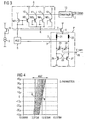
- FIG. 3 shows an embodiment of the proposed principle applied to an LC oscillator 1.
- the oscillator 1 is designed as a tunable LC resonant circuit and as such comprises two fixed value inductors 21, 22, two tunable capacitors 23, 24 and a de-attenuation amplifier 25, which comprises two cross-coupled p-channel transistors 26, 27.
- the inductors 21, 22 connect the supply current input 4 of the oscillator 1 "with the output terminal pair 3, 3 'of the oscillator 1".
- the tuning input 28 of the oscillator to which a tuning signal can be supplied, is connected via a respective varactor 23, 24 to the output terminals 3, 3 '.
- the sources of transistors 26, 27 are grounded. Depending on a gate terminal of the transistors 26, 27 is connected to a respective drain terminal of the other transistor to form a cross-coupling.
- the two drain terminals of the EntdämpfungsverEntrs 25 form the outputs 3, 3 'of the LC oscillator.
- the snubber amplifier 25 provides a negative resistance or a negative impedance.
- the time constant of the amplitude control 5, 6, 7 is interpreted much faster than the time constant of the oscillator.
- the achievable with the proposed circuit frequency deviation ranges from 10 KHz to a few megahertz.
- the possible data rate is up to several Mbit per second.
- FIG. 4 shows, on the basis of a diagram, the resonant frequency of the quartz oscillator of FIG. 2 as a function of the amplification of the amplitude control loop.
- the diagram is given in an S parameter representation.
- the loop gain is provided as a share parameter. It can be seen that varying the gain of the amplitude control loop covers a range of approximately 1800 hertz can.
- the graph thus proves the functionality of the proposed principle, namely the implementation of a frequency shift keying by switchable amplitude control of an oscillator.
- the time constant of the controller is preferably designed so that it does not respond to short-term frequency changes caused by the frequency modulation.
Landscapes
- Engineering & Computer Science (AREA)
- Computer Networks & Wireless Communication (AREA)
- Signal Processing (AREA)
- Oscillators With Electromechanical Resonators (AREA)
- Stabilization Of Oscillater, Synchronisation, Frequency Synthesizers (AREA)
- Inductance-Capacitance Distribution Constants And Capacitance-Resistance Oscillators (AREA)
- Magnetic Resonance Imaging Apparatus (AREA)
- Amplitude Modulation (AREA)
- Transmitters (AREA)
Abstract
Description
Die vorliegende Erfindung betrifft eine Oszillatoranordnung, die für eine Frequenzmodulation ausgelegt ist.The present invention relates to an oscillator arrangement designed for frequency modulation.
Unter den digitalen Modulationsverfahren ist die Frequenzumtastung, englisch: frequency shift keying, FSK, neben der Amplitudenumtastung und der Phasenumtastung sowie Kombinationen der genannten Verfahren, eine verbreitete Methode zur digitalen Modulation eines Trägersignals.Among the digital modulation techniques, Frequency Shift Keying (FSK), in addition to amplitude shift keying and phase shift keying, as well as combinations of these methods, is a common method for digital modulation of a carrier signal.
Eine Möglichkeit, ein Trägersignal mit einer Frequenzumtastung zu beaufschlagen, besteht darin, das Trägersignal unmittelbar bei seiner Erzeugung im Oszillator zu modulieren.One way to apply a carrier to frequency shift keying is to modulate the carrier signal as it is being generated in the oscillator.
Dabei wird die Frequenzumtastung des Oszillators üblicherweise dadurch erreicht, daß kleine, frequenzbestimmende Kapazitäten zu einem im Oszillator gebildeten Schwingkreis hinzu- oder weggeschaltet werden. Hierdurch wird das digitale Modulationssignal mit dem gewünschten Frequenzhub auf den Träger aufmoduliert.In this case, the frequency shift keying of the oscillator is usually achieved by adding or disconnecting small, frequency-determining capacitances to a resonant circuit formed in the oscillator. As a result, the digital modulation signal is modulated onto the carrier with the desired frequency deviation.
Der Oszillator kann dabei beispielsweise als Quarzoszillator oder als LC-Oszillator ausgeführt sein. Während bei einem Quarzoszillator die Schwingfrequenz hauptsächlich durch die Schwingfrequenz des Quarzes bestimmt wird, beeinflussen beim LC-Oszillator zumindest eine Induktivität und zumindest eine Kapazität die Schwingfrequenz.The oscillator can be embodied for example as a quartz oscillator or as an LC oscillator. While in a quartz oscillator, the oscillation frequency is mainly determined by the oscillation frequency of the quartz, at least one inductance and at least one capacitance influence the oscillation frequency in the case of the LC oscillator.
Um beispielsweise einen Frequenzhub von 60 KHz zu erzeugen, müssen jedoch verhältnismäßig große Kapazitäten in dem sogenannten Oszillator-Tank zu- und weggeschaltet werden. Das Schalten von Kapazitäten jedoch bringt jedoch stets Probleme bezüglich Ladungsinjektionen mit sich. Es werden unerwünschte Interferenzen sowohl in die Stromversorgung des Oszillators, als auch in den Substratanschluß eines integrierten Oszillators hineingetragen. Die Ladungen bewirken eine Störbeeinflussung des Oszillators, beispielsweise eines spannungsgesteuerten Oszillators, und beeinflussen auch dessen Ausgangsspektrum in störender Weise. Außerdem ist ein verhältnismäßig großer Chipflächenbedarf zum Integrieren der zuschaltbaren Kapazitäten nötig.For example, to produce a frequency sweep of 60 KHz, however, relatively large capacities in the so-called oscillator tank must be switched on and off. However, switching capacitances always involves problems with charge injections. There will be unwanted interference both in the power supply of the oscillator, as well as carried in the substrate terminal of an integrated oscillator. The charges cause interference of the oscillator, such as a voltage controlled oscillator, and also affect its output spectrum in a disturbing way. In addition, a relatively large chip area requirement for integrating the switchable capacities is necessary.
Das Dokument US 2,874,216 betrifft ein automatisches Signalsteuersystem.The document US 2,874,216 relates to an automatic signal control system.
Aufgabe der vorliegenden Erfindung ist es, eine Oszillatoranordnung anzugeben, die für eine Modulation gemäß einem Frequenzumtastungsverfahren geeignet ist und bei der durch Ladungsinjektion bedingte Probleme vermieden oder signifikant verringert sind.The object of the present invention is to provide an oscillator arrangement which is suitable for a modulation according to a frequency shift keying method and in which problems caused by charge injection are avoided or significantly reduced.
Erfindungsgemäß wird die Aufgabe gelöst durch eine Oszillatoranordnung für Frequenzmodulation, aufweisend
- einen Steuereingang zum Zuführen eines Modulationssignals,
- einen Oszillatorausgang zum Abgreifen eines frequenzmodulierten Signals,
- einen Oszillator mit einem Eingang zur Zuführung eines Speisestroms und mit dem Oszillatorausgang,
- einen Regelkreis zur Amplitudenregelung mit einem Eingang, der an den Oszillatorausgang angeschlossen ist und mit einem Ausgang, der mit dem Eingang zur Zuführung eines Speisestroms des Oszillators verbunden ist, und
- ein Mittel zur Beeinflussung des Speisestroms in Abhängigkeit von dem Modulationssignal, das in dem Regelkreis angeordnet und mit dem Eingang des Oszillators zur Zuführung eines Speisestroms gekoppelt ist.
- a control input for supplying a modulation signal,
- an oscillator output for picking up a frequency modulated signal,
- an oscillator with an input for supplying a supply current and with the oscillator output,
- a control loop for controlling the amplitude with an input connected to the oscillator output and having an output connected to the input for supplying a supply current of the oscillator, and
- a means for influencing the supply current in response to the modulation signal, which is arranged in the control loop and coupled to the input of the oscillator for supplying a supply current.
Gemäß dem vorgeschlagenen Prinzip wird die bei einem gesteuerten Oszillator mit Frequenzmodulation normalerweise ohnehin meist vorhandene, automatische Amplitudenregelung dazu mitbenutzt, um den Betriebsstrom des Oszillators zu steuern und damit auch die Oszillatorfrequenz in gewünschter Weise zu beeinflussen, das heißt zu modulieren. Der Oszillator wird demnach dadurch moduliert, daß die Schleifenverstärkung der Verstärkungsregelungsschleife durch Beeinflussen des Speisestroms des Oszillators gesteuert wird.In accordance with the proposed principle, the automatic amplitude control, which is usually present anyway in a controlled oscillator with frequency modulation, is also used to control the operating current of the oscillator and so that the oscillator frequency in the desired manner to influence, that is to modulate. The oscillator is thus modulated by the loop gain of the gain control loop is controlled by influencing the supply current of the oscillator.
Bevorzugt wird der Amplitudenregelkreis dazu mitbenutzt, den sogenannten Basisstrom des Oszillators mittels durch das Modulationssignal gesteuerte Stromabzugstechnik zu verändern und damit auch die Frequenz in kleinen Schritten zu verändern.Preferably, the amplitude control loop is used to change the so-called base current of the oscillator by means of the modulation signal controlled Stromabzugstechnik and thus to change the frequency in small steps.
Das vorgeschlagene Prinzip ist unter anderem sowohl bei LC-Oszillatoren als auch bei Quarz-Oszillatoren mit Vorteil anwendbar.The proposed principle is advantageously applicable, inter alia, both in LC oscillators and quartz oscillators.
Bei dem vorgeschlagenen Prinzip kann vollständig auf umschaltbare Kapazitäten zur Frequenzumtastung verzichtet werden. Dadurch ist das Problem der Ladungsinjektion vermieden, es treten keine unerwünschten Rückwirkungen auf die Stromversorgung auf und zusätzlich ist die Schaltung ist mit besonders geringem Chipflächenbedarf realisierbar. Außerdem kann die Ansteuerung des Mittels zur Beeinflussung des Speisestroms in Abhängigkeit von dem Modulationssignal mit einem einfach aufgebauten Steuerblock realisiert werden.In the proposed principle can be completely dispensed with switchable capacity for Frequenzumtastung. As a result, the problem of charge injection is avoided, there are no undesirable effects on the power supply and, in addition, the circuit can be realized with a particularly small chip area requirement. In addition, the control of the means for influencing the supply current in response to the modulation signal can be realized with a simple control block.
Das Mittel zur Beeinflussung des Speisestroms umfaßt bevorzugt mehrere, bezüglich ihrer geschalteten Strecken parallel geschaltete Stromschalter. Abhängig vom Modulationssignal werden die parallel geschalteten Stromschalter dabei bevorzugt so angesteuert, daß gerade der zur gewünschten Frequenzverstimmung nötige Strom abgezogen wird.The means for influencing the supply current preferably comprises a plurality of current switches connected in parallel with respect to their connected paths. Depending on the modulation signal, the parallel-connected current switches are preferably controlled so that just the current required for the desired frequency detuning current is subtracted.
Die parallel geschalteten Stromschalter sind bevorzugt ausgangsseitig in einem Stromspiegel angeordnet. Dabei bilden bevorzugt je ein Transistor des Stromspiegels und ein diesem zugeordneter Schalter eine Serienschaltung. Die Serienschaltungen sind dabei zueinander parallelgeschaltet. Die Schalter können unabhängig voneinander zu- und abgeschaltet werden. Durch Steuern der Schleifenverstärkung der automatischen Regelschleife mittels entsprechender Ansteuerung der Stromschalter kann mit Vorteil in einfacher Weise die Frequenz des Oszillators durch Stromsteuerung moduliert werden.The parallel-connected current switches are preferably arranged on the output side in a current mirror. In this case, preferably each one transistor of the current mirror and a switch associated therewith form a series circuit. The series circuits are connected in parallel to each other. The switches can be switched on and off independently of each other. By controlling the loop gain of the automatic control loop By means of appropriate control of the current switch, the frequency of the oscillator can advantageously be modulated by current control in a simple manner.
Der Stromspiegel mit den parallel geschalteten Stromschaltern wirkt bevorzugt auf einen weiteren Stromspiegel, der eine Speisestromquelle zum Speisen des Oszillators mit dem Oszillator koppelt. Der Schaltungsknoten, an dem der Stromspiegel mit den Stromschaltern in die Speisestromzuführung des Oszillators eingreift, ist dabei bevorzugt an dem gemeinsamen Gate-Anschluß bzw. Basis-Anschluß der Stromspiegeltransistoren im weiteren Stromspiegel vorgesehen. Dadurch wird in Abhängigkeit von dem Modulationssignal ein Teil des von der Konstantstromquelle bereitgestellten Stroms mit den Stromschaltern abgezogen und somit die Oszillatorfrequenz moduliert.The current mirror with the parallel-connected current switches preferably acts on a further current mirror, which couples a supply current source for supplying the oscillator with the oscillator. The circuit node at which the current mirror engages with the current switches in the supply current supply of the oscillator is preferably provided at the common gate terminal or base terminal of the current mirror transistors in the further current mirror. As a result, depending on the modulation signal, a part of the current provided by the constant current source is drawn off with the current switches and thus the oscillator frequency is modulated.
Zur Ansteuerung der Stromschalter ist bevorzugt ein Steuerblock vorgesehen mit einem Eingang, an dem das Modulationssignal zugeführt wird und mit einem oder mehreren Ausgängen, die mit jeweiligen Steueranschlüssen der zugeordneten Stromschalter verbunden sind.To control the current switch, a control block is preferably provided with an input to which the modulation signal is supplied and with one or more outputs which are connected to respective control terminals of the associated power switch.
Das Modulationssignal ist bevorzugt ein digital codiertes Signal, welches gemäß einem Frequenzumtastungsverfahren, englisch: frequency shift keying, FSK, codiert ist.The modulation signal is preferably a digitally coded signal, which is coded according to a frequency shift keying method, FSK.
Der Oszillator ist bevorzugt abstimmbar ausgeführt mit einem weiteren Steuereingang, an dem ein Abstimmsignal zuführbar ist und mit einer Schwingfrequenz-bestimmenden Kapazität, die in Abhängigkeit von dem Abstimmsignal gesteuert wird. Derartige, abstimmbare Kapazitäten sind bevorzugt als Varaktordioden ausgeführt. Somit ist ein spannungsgesteuerter Oszillator, englisch: voltage controlled oszillator, VCO realisiert.The oscillator is preferably designed to be tunable with a further control input, to which a tuning signal can be fed and with an oscillation frequency-determining capacitor, which is controlled in dependence on the tuning signal. Such tunable capacitances are preferably designed as varactor diodes. Thus, a voltage controlled oscillator, English: voltage controlled oscillator, VCO realized.
Weitere Einzelheiten und vorteilhafte Ausgestaltungen des vorgeschlagenen Prinzips sind Gegenstand der Unteransprüche.Further details and advantageous embodiments of the proposed principle are the subject of the dependent claims.
Die Erfindung wird nachfolgend an mehreren Ausführungsbeispielen anhand der Zeichnungen näher erläutert.The invention will be explained in more detail below with reference to several embodiments with reference to the drawings.
Es zeigen:
Figur 1- ein Blockschaltbild einer beispielhaften Oszillatoranordnung für Frequenzmodulation gemäß dem vorgeschlagenen Prinzip,
Figur 2- eine Weiterbildung der Oszillatoranordnung von
Figur 1, ausgelegt für einen Quarzoszillator, Figur 3- ein weiteres Ausführungsbeispiel einer Oszillatoranordnung gemäß
Figur 1 mit LC-Oszillator und Figur 4- die Resonanzfrequenz in Abhängigkeit der Schleifenverstärkung der Amplitudenregelung anhand eines S-Parameter-Diagramms bei einem Quarzoszillator gemäß
Figur 2.
- FIG. 1
- a block diagram of an exemplary oscillator arrangement for frequency modulation according to the proposed principle,
- FIG. 2
- A development of the oscillator arrangement of FIG. 1, designed for a quartz oscillator,
- FIG. 3
- a further embodiment of an oscillator arrangement according to Figure 1 with LC oscillator and
- FIG. 4
- the resonant frequency as a function of the loop gain of the amplitude control using an S-parameter diagram in a quartz oscillator according to Figure 2.
Figur 1 zeigt eine Oszillatoranordnung ausgelegt für Frequenzmodulation. Diese umfaßt einen Oszillator 1 sowie einen Steuereingang 2 zum Zuführen eines Modulationssignals. Der Oszillator 1 hat einen Ausgang 3, an dem ein frequenzmoduliertes Signal abgreifbar ist. Außerdem weist der Oszillator 1 einen Eingang 4 zum Zuführen eines Speisestroms auf. Der Speisestrom wird unter anderem zur Entdämpfung des Schwingkreises benutzt, der in dem Oszillator 1 gebildet ist. Der Speisestrom wird auch als Basisstrom oder tail current bezeichnet. Um die Stabilität des Oszillators zu gewährleisten, ist dieser in einem Amplitudenregelkreis angeordnet. Der Regelkreis zur Amplitudenregelung umfaßt einen AGC-Block 5, einen ersten Stromspiegel 6 und einen zweiten Stromspiegel 7, 8. Der Ausgang des ersten Stromspiegels 6 steuert einen Stromquellentransistor 7 an, der an seinem Stromquellenausgang mit dem Speisestromeingang 4 des Oszillators 1 verbunden ist. Eine Transistordiode 8 bildet mit dem Stromquellentransistor 7 den zweiten Stromspiegel. Der gemeinsame Gate-Anschluß der Transistoren 7, 8, der mit dem Ausgang des ersten Stromspiegels 6 verbunden ist, ist als Schaltungsknoten K bezeichnet. Der Eingang des zweiten Stromspiegels 7, 8 ist an eine Stromquelle 9 angeschlossen, die einen Bezugsstrom für den Oszillator 1 bereitstellt. Der Stromspiegel 6 umfaßt eine Transistordiode M1 sowie ausgangsseitig insgesamt vier parallel geschaltete Stromspiegeltransistoren M2, M3, M4, M5, welche unabhängig voneinander zu- und abschaltbar sind. Hierfür ist je ein Schalter 10, 11, 12, 13 vorgesehen, der jeweils einen Bezugspotentialanschluß 14 mit einem Lastanschluß der gesteuerten Strecken des zugeordneten Transistors M2, M3, M4, M5 verbindet, vorliegend mit deren Source-Anschluß. Dabei sind die Gate-Anschlüsse der Feldeffekttransistoren M1 bis M5 im Stromspiegel 6 unmittelbar miteinander verbunden. Damit der Transistor M1 als Diode arbeitet, ist dessen Gate-Anschluß mit seinem Drain-Anschluß unmittelbar verbunden. Der Source-Anschluß des n-Kanal-Feldeffekttransistors M1 ist an Bezugspotentialanschluß 14 angeschlossen. Die Drain-Anschlüsse der Transistoren M2 bis M5 sind unmittelbar miteinander verbunden in dem Schaltungsknoten K und bilden den Ausgang des Stromspiegels 6. Der Schaltungsknoten K ist unmittelbar an die Gate-Anschlüsse der Stromspiegeltransistoren 7, 8 angeschlossen.FIG. 1 shows an oscillator arrangement designed for frequency modulation. This comprises an
Die Schalter 10, 11, 12, 13, die als Stromschalter ausgelegt sind, werden gesteuert durch eine Steuerlogik, die in einem entsprechenden Steuerblock 15 vorgesehen ist, dessen Eingang den Steuereingang 2 zum Zuführen eines Modulationssignals der Oszillatoranordnung bildet und dessen Ausgang mit den Steueranschlüssen der Schalter 10, 11, 12, 13 verbunden ist.The
Ein eventuell vorhandener Abstimmeingang des spannungsgesteuerten Oszillators 1 ist in Figur 1 nicht dargestellt.A possibly existing tuning input of the voltage-controlled
Die Besonderheit der Schaltung gemäß Figur 1 ist es, daß die Modulationsdaten nicht unmittelbar im Oszillatorkern vorgesehene schaltbare Kapazitäten steuern, welche somit die Schwingfrequenz des Oszillators beeinflussen, sondern daß die Modulationsdaten in die Amplitudenregelung des Oszillators 1 eingreifen. Die Oszillatorfrequenz wird dabei indirekt über die Steuerung des Speisestroms des Oszillators, englisch tail current, umgetastet. Der Amplitudenregelkreis 5, 6, 7 umfaßt schaltbare Stromspiegel, mit denen die Frequenz des Oszillators verstellt werden kann. Das Modulationssignal steuert demnach die Schleifenverstärkung des Amplitudenregelkreises 5, 6, 7. Mit den Stromschaltern wird die Frequenzumsteuerung des Oszillators 1 dabei in einer Stromabzugstechnik realisiert. Somit kann mit Vorteil auf umschaltbare Kapazitäten zur Frequenzumtastung im Oszillator verzichtet werden. Damit sind Vorteile erzielt bezüglich Ladungsinjektion, Rückwirkungen auf die Leistungsversorgung, einfacher Ansteuerung und Chipfläche.The peculiarity of the circuit according to FIG. 1 is that the modulation data does not control switchable capacitors provided directly in the oscillator core, which thus influence the oscillation frequency of the oscillator, but that the modulation data intervene in the amplitude regulation of the
Figur 2 zeigt ein weiteres Ausführungsbeispiel der vorliegenden Oszillatoranordnung, welche einen als Quarzoszillator 1' realisierten Oszillator aufweist. Die Amplitudenregelung einschließlich der schaltbaren Stromquellen im Amplitudenregelkreis und deren Ansteuerung mit dem Modulationssignal entsprechen denjenigen von Figur 1. Insoweit wird deren Beschreibung nicht wiederholt. Der Oszillator 1' bei Figur 2 ist als Quarzoszillator ausgeführt und umfaßt einen Schwingquarz 16. Beide Anschlüsse des Schwingquarzes 16 sind über je einen Kondensator 17, 18 mit Bezugspotential verbunden. Zur Entdämpfung des schwingfähigen Systems ist ein Verstärker vorgesehen, der einen p-Kanal-Feldeffekttransistor 19 umfaßt. Der Gate-Anschluß des Transistors 19, an dem zugleich der Ausgang 3 des Oszillators gebildet ist, ist mit einem der beiden Anschlüsse des Quarzes 16 verbunden. Der Source-Anschluß des Transistors 19 ist auf Bezugspotential gelegt. Der Drain-Anschluß des Transistors 19, der den Eingang zur Zuführung eines Speisestroms 4 des Oszillators 1' bildet, ist zum einen über einen Widerstand 20 mit dem Gate-Anschluß des Transistors 19 verbunden und zum anderen mit dem weiteren Anschluß des Quarzes 16 verbunden. Bei der Schaltung von Figur 2 ist ein Frequenzhub möglich von 10 KHz bis 100 KHz durch entsprechendes Schalten der Stromschalter 10, 11, 12, 13 in Abhängigkeit vom Modulationssignal. Die Datenrate kann zwischen 0 und 20 kBit/sec betragen. Um eine Selbstmischung zu vermeiden, sollte die Zeitkonstante der Amplitudenregelung des Amplitudenregelkreises 5, 6, 7 deutlich kleiner eingestellt werden als die Zeitkonstante des Oszillators. Bei dem vorliegenden Quarzoszillator wird die Frequenz über den Strom und in weiterer Folge über die sich einstellende Amplitude verändert. Durch Verwendung einer Amplitudenregelung kann mittels digital gesteuerter Stromabzugstechnik der Oszillator-Basisstrom und damit auch die Frequenz verändert werden. Bei Frequenzhüben von bis zu plus minus 100 KHz treten lediglich geringe Ladungsverschiebungen auf. Mit anwendungsabhängiger Gewichtung der Transistoren M1 bis M5 kann praktisch jeder beliebige, gewünschte Frequenzhub innerhalb der beschriebenen Grenzen eingestellt werden.FIG. 2 shows a further exemplary embodiment of the present oscillator arrangement, which has an oscillator realized as quartz oscillator 1 '. The amplitude control including the switchable current sources in the amplitude control loop and their control with the modulation signal correspond to those of Figure 1. In that regard, the description is not repeated. The oscillator 1 'in Figure 2 is designed as a quartz oscillator and comprises a
Gemäß dem vorgeschlagenen Prinzip tritt keine Ladungsinjektion auf, unerwünschte Rückwirkungen von Störsignalen auf die Stromversorgung werden vermieden, die Schaltungen sind auf verhältnismäßig geringer Chipfläche integrierbar und die Ansteuerung der Stromschalter kann mit einer besonders einfach aufgebauten Steuerlogik 15 realisiert werden.According to the proposed principle, no charge injection occurs, unwanted effects of interference signals on the power supply are avoided, the circuits can be integrated on a relatively small chip area and the control of the power switch can be realized with a particularly
Figur 3 zeigt ein Ausführungsbeispiel des vorgeschlagenen Prinzips angewendet auf einen LC-Oszillator 1". Abgesehen von der Ausführungsform des Oszillators 1" entspricht der Aufbau der Oszillatoranordnung von Figur 3 in den verwendeten Bauteilen, deren Verschaltung miteinander und der vorteilhaften Funktionsweise weitestgehend derjenigen von Figur 1 und wird an dieser Stelle soweit nicht noch einmal wiederholt. Der Oszillator 1" ist als abstimmbarer LC-Schwingkreis ausgeführt. Als solcher umfaßt er zwei Festwert-Induktivitäten 21, 22, zwei abstimmbare Kapazitäten 23, 24 und einen Entdämpfungsverstärker 25, welcher zwei kreuzgekoppelte p-Kanal-Transistoren 26, 27 umfaßt. Die Induktivitäten 21, 22 verbinden den Speisestromeingang 4 des Oszillators 1" mit dem Ausgangsklemmenpaar 3, 3' des Oszillators 1". Der Abstimmeingang 28 des Oszillators, an dem ein Tuningsignal zuführbar ist, ist über je einen Varaktor 23, 24 an die Ausgangsklemmen 3, 3' gelegt. Die Source-Anschlüsse der Transistoren 26, 27 sind gegen Masse geschaltet. Je ein Gate-Anschluß der Transistoren 26, 27 ist mit je einem Drain-Anschluß des jeweils anderen Transistors unter Bildung einer Kreuzkopplung verbunden. Die beiden Drain-Anschlüsse des Entdämpfungsverstärkers 25 bilden die Ausgänge 3, 3' des LC-Oszillators. Der Entdämpfungsverstärker 25 liefert einen negativen Widerstand oder eine negative Impedanz.3 shows an embodiment of the proposed principle applied to an
Um eine Selbstmischung zu vermeiden, ist die Zeitkonstante der Amplitudenregelung 5, 6, 7 sehr viel schneller auszulegen als die Zeitkonstante des Oszillators. Der mit der vorgeschlagenen Schaltung erzielbare Frequenzhub reicht von 10 KHz bis zu einigen Megahertz. Die mögliche Datenrate reicht bis zu einigen Mbit pro Sekunde.In order to avoid self-mixing, the time constant of the
Die Vorteile der Schaltung von Figur 2, nämlich Vermeidung unerwünschter Ladungsinjektion, Vermeidung unerwünschter Interferenzen auf die Stromversorgung der Schaltung, Implementierbarkeit auf geringer Chipfläche und einfach aufgebaute Steuerlogik 15 bleiben auch bei der Schaltung von Figur 3 erhalten.The advantages of the circuit of FIG. 2, namely the avoidance of unwanted charge injection, the avoidance of undesired interference with the circuit power supply, the implementability on a small chip area and the
Figur 4 zeigt anhand eines Schaubildes die Resonanzfrequenz des Quarzoszillators von Figur 2 abhängig von der Verstärkung der Amplitudenregelschleife. Das Schaubild ist dabei in einer S-Parameter-Darstellung angegeben. Dabei ist als Schar-Parameter die Schleifenverstärkung vorgesehen. Man erkennt, daß durch Variieren der Verstärkung des Amplitudenregelkreises ein Bereich von ungefähr 1800 Hertz abgedeckt werden kann. Das Schaubild belegt demnach die Funktionsfähigkeit des vorgeschlagenen Prinzips, nämlich die Durchführung einer Frequenzumtastung durch schaltbare Amplitudenregelung eines Oszillators.FIG. 4 shows, on the basis of a diagram, the resonant frequency of the quartz oscillator of FIG. 2 as a function of the amplification of the amplitude control loop. The diagram is given in an S parameter representation. In this case, the loop gain is provided as a share parameter. It can be seen that varying the gain of the amplitude control loop covers a range of approximately 1800 hertz can. The graph thus proves the functionality of the proposed principle, namely the implementation of a frequency shift keying by switchable amplitude control of an oscillator.
Bei Einbettung des beschriebenen, abstimmbaren Oszillators in einer Phasenregelschleife (PLL) ist bevorzugt die Zeitkonstante des Reglers so ausgelegt, daß dieser nicht auf kurzfristige Frequenzänderungen, die durch die Frequenzmodulation bedingt sind, reagiert.When embedding the described tunable oscillator in a phase-locked loop (PLL), the time constant of the controller is preferably designed so that it does not respond to short-term frequency changes caused by the frequency modulation.
Claims (9)
- Oscillator arrangement for frequency modulation, comprising- a control input (2) for supplying a modulation signal (FSK),- an oscillator output (3) for tapping a frequency-modulated signal,- an oscillator (1) with an input (4) for supplying a feed current and with an oscillator output (3),- a control circuit for amplitude control (5, 6, 7) with an input that is connected to the oscillator output (3) and with an output that is connected to the input (4) for supplying a feed current for the oscillator (1), and- a means for influencing the feed current (6) in dependence on the modulation signal (FSK), wherein said means is arranged in the control circuit (5, 6, 7) and coupled to the input (4) of the oscillator for supplying a feed current.
- Oscillator arrangement according to Claim 1,
characterized in that
the means for influencing the feed current (6) comprises several parallel-connected current switches (10, 11, 12, 13). - Oscillator arrangement according to Claim 2,
characterized in that
the parallel-connected current switches (10, 11, 12, 13) are arranged in current paths of one respective current mirror (M1, M2, M3, M4, M5) on its output side. - Oscillator arrangement according to Claim 3,
characterized in that
the current mirrors (M1, M2, M3, M4, M5) connect the output of a gain control block (5) connected to the oscillator output (3) with a circuit node (K) in another current mirror (7, 8) that is designed for supplying the feed current for the oscillator (1). - Oscillator arrangement according to one of Claims 2-4,
characterized in that
a control block (15) is provided that has an input forming the control input (2) of the oscillator arrangement for supplying a modulation signal (FSK) and outputs that are connected to the control inputs of the current switches (10, 11, 12, 13), wherein said control block is designed for controlling the current switches (10, 11, 12, 13) in dependence on the modulation signal (FSK). - Oscillator arrangement according to one of Claims 1-5,
characterized in that
the modulation signal (FSK) is a signal that is digitally coded in accordance with a frequency shift keying method. - Oscillator arrangement according to one of Claims 1-6,
characterized in that
the oscillator (1) is realized in the form of a tunable oscillator that comprises at least one capacitance (23) that can be adjusted in dependence on a tuning voltage (V_tune) and determines the oscillation frequency. - Oscillator arrangement according to one of Claims 1-7,
characterized in that
the oscillator (1) is realized in the form of an LC-oscillator that comprises at least one capacitance (23) that determines the frequency of the resonant circuit and at least one inductance (21) that determines the frequency of the resonant circuit. - Oscillator arrangement according to one of Claims 1-7,
characterized in that
the oscillator (1) is realized in the form of a crystal oscillator with an oscillator crystal (16) that determines the oscillation frequency.
Applications Claiming Priority (3)
| Application Number | Priority Date | Filing Date | Title |
|---|---|---|---|
| DE10302391 | 2003-01-22 | ||
| DE10302391A DE10302391A1 (en) | 2003-01-22 | 2003-01-22 | Oscillator arrangement for frequency modulation |
| PCT/EP2003/014461 WO2004066578A1 (en) | 2003-01-22 | 2003-12-18 | Oscillator device for frequency modulation |
Publications (2)
| Publication Number | Publication Date |
|---|---|
| EP1586183A1 EP1586183A1 (en) | 2005-10-19 |
| EP1586183B1 true EP1586183B1 (en) | 2006-11-22 |
Family
ID=32694925
Family Applications (1)
| Application Number | Title | Priority Date | Filing Date |
|---|---|---|---|
| EP03782441A Expired - Fee Related EP1586183B1 (en) | 2003-01-22 | 2003-12-18 | Oscillator device for frequency modulation |
Country Status (6)
| Country | Link |
|---|---|
| US (1) | US7369009B2 (en) |
| EP (1) | EP1586183B1 (en) |
| AT (1) | ATE346445T1 (en) |
| AU (1) | AU2003290081A1 (en) |
| DE (2) | DE10302391A1 (en) |
| WO (1) | WO2004066578A1 (en) |
Families Citing this family (11)
| Publication number | Priority date | Publication date | Assignee | Title |
|---|---|---|---|---|
| JP2007251228A (en) * | 2006-03-13 | 2007-09-27 | Toshiba Corp | Voltage-controlled oscillator, operating current adjusting device, and operation current adjustment method of the voltage-controlled oscillator |
| TWI323565B (en) * | 2006-06-16 | 2010-04-11 | Realtek Semiconductor Corp | Voltage-controlled oscillator |
| US7425909B2 (en) * | 2006-07-31 | 2008-09-16 | Analog Devices, Inc. | Low-noise programmable current source |
| WO2009049143A1 (en) * | 2007-10-10 | 2009-04-16 | Georgia Tech Research Corporation | Millimeter-wave wideband voltage controlled oscillator |
| US7639097B2 (en) * | 2007-10-11 | 2009-12-29 | Freescale Semiconductor, Inc. | Crystal oscillator circuit having fast start-up and method therefor |
| US20150180412A1 (en) * | 2013-12-24 | 2015-06-25 | Realtek Semiconductor Corp. | Controllable oscillator and method thereof |
| JP6930134B2 (en) * | 2017-02-28 | 2021-09-01 | セイコーエプソン株式会社 | Oscillators, electronics and mobiles |
| EP3514951B1 (en) * | 2018-01-18 | 2024-03-13 | ams AG | Oscillator circuit arrangement |
| US10833633B2 (en) * | 2018-12-19 | 2020-11-10 | Semiconductor Components Industries, Llc | Circuit and method for controlling a crystal oscillator |
| TWI763116B (en) * | 2020-11-10 | 2022-05-01 | 瑞昱半導體股份有限公司 | Oscillating signal generator circuit |
| CN114510101A (en) * | 2020-11-16 | 2022-05-17 | 瑞昱半导体股份有限公司 | Oscillation signal generating circuit |
Family Cites Families (12)
| Publication number | Priority date | Publication date | Assignee | Title |
|---|---|---|---|---|
| US2874216A (en) | 1953-10-27 | 1959-02-17 | Gen Electric | Automatic signal control system |
| US3641460A (en) | 1970-11-09 | 1972-02-08 | Intertel Inc | Frequency shift transmitter |
| US4071832A (en) * | 1976-06-14 | 1978-01-31 | Sperry Rand Corporation | Current controlled oscillator |
| CA1215437A (en) * | 1983-05-25 | 1986-12-16 | Sony Corporation | Variable frequency oscillating circuit |
| JPH0248807A (en) | 1988-08-10 | 1990-02-19 | Hitachi Ltd | Modulation circuit |
| DE3836822A1 (en) * | 1988-10-28 | 1990-05-03 | Olympia Aeg | Frequency modulator with PLL for transmitting optionally NRZ data signals or voice signals |
| JPH0332206A (en) | 1989-06-29 | 1991-02-12 | Nippon Denki Musen Denshi Kk | Frequency modulator |
| US5150377A (en) | 1990-11-02 | 1992-09-22 | At&T Bell Laboratories | Direct sequence spread spectrum (dsss) communications system with frequency modulation utilized to achieve spectral spreading |
| US5323125A (en) * | 1993-03-15 | 1994-06-21 | Motorola, Inc. | Frequency agile method for transmitting multi-level data |
| US5687201A (en) | 1995-03-21 | 1997-11-11 | Standard Microsystems Corporation | Phase-locked-loop with linear combination of charge pump and current controlled oscillator |
| US6198360B1 (en) * | 1998-10-16 | 2001-03-06 | Cypress Semiconductor Corp. | Quadrature current frequency modulation oscillator |
| US6323735B1 (en) * | 2000-05-25 | 2001-11-27 | Silicon Laboratories, Inc. | Method and apparatus for synthesizing high-frequency signals utilizing on-package oscillator circuit inductors |
-
2003
- 2003-01-22 DE DE10302391A patent/DE10302391A1/en not_active Ceased
- 2003-12-18 EP EP03782441A patent/EP1586183B1/en not_active Expired - Fee Related
- 2003-12-18 DE DE50305801T patent/DE50305801D1/en not_active Expired - Lifetime
- 2003-12-18 AU AU2003290081A patent/AU2003290081A1/en not_active Abandoned
- 2003-12-18 WO PCT/EP2003/014461 patent/WO2004066578A1/en not_active Application Discontinuation
- 2003-12-18 US US10/542,719 patent/US7369009B2/en not_active Expired - Fee Related
- 2003-12-18 AT AT03782441T patent/ATE346445T1/en active
Also Published As
| Publication number | Publication date |
|---|---|
| ATE346445T1 (en) | 2006-12-15 |
| US20060103475A1 (en) | 2006-05-18 |
| DE50305801D1 (en) | 2007-01-04 |
| DE10302391A1 (en) | 2004-08-12 |
| WO2004066578A1 (en) | 2004-08-05 |
| EP1586183A1 (en) | 2005-10-19 |
| AU2003290081A1 (en) | 2004-08-13 |
| US7369009B2 (en) | 2008-05-06 |
Similar Documents
| Publication | Publication Date | Title |
|---|---|---|
| DE60317669T2 (en) | LC OSCILLATOR WITH LARGE TUNING RANGE AND LOW PHASE NOISE | |
| DE102006011285B4 (en) | Oscillating circuit arrangement with digital control, method for generating a vibration signal and digital phase locked loop with the resonant circuit arrangement | |
| DE60110686T2 (en) | frequency synthesizer | |
| DE60030589T2 (en) | METHOD OF CONTROL VOLTAGE SUPPLY FOR VARACTERORS FOR REDUCING PHASE RUSH IN ELECTRONIC OSCILLATORS | |
| DE69533913T2 (en) | frequency synthesizer | |
| DE602005003396T2 (en) | Variable capacitance circuit with ON / OFF switch for the variable capacitance function and same voltage controlled oscillator using | |
| DE102014102940A1 (en) | Oscillator with LC primary and secondary oscillations | |
| EP1586183B1 (en) | Oscillator device for frequency modulation | |
| EP1195000B1 (en) | Voltage-controlled oscillator with lc resonant circuit | |
| EP1069680A2 (en) | Tuner with at least a first and a second frequency band | |
| DE102012105968A1 (en) | oscillator circuit | |
| EP1223670B1 (en) | Voltage controlled oscillator for frequency modulation | |
| DE2603641A1 (en) | RIGID RETURN LOOP, IN PARTICULAR FOR A BROADBAND TRANSMITTER | |
| EP0623992B1 (en) | Oscillator | |
| DE19949782C1 (en) | Phase-locked-loop circuit has charge pumping mechanism controlled by phase error, low-pass filter and inverter stage bias voltage generator between latter and voltage-controlled ring oscillator | |
| EP1670136A1 (en) | Voltage controlled oscillator with analogue and digital control | |
| DE2946194A1 (en) | CHANNEL SELECTOR WITH FREQUENCY SYNTHESATOR | |
| DE60009908T2 (en) | VARIABLE OSCILLATOR | |
| DE102004025545A1 (en) | CMOS LC tank Oscillator | |
| DE3931513C2 (en) | ||
| DE19837204B4 (en) | Dead-time reduction in frequency jumps in multiband synthesis units | |
| WO2005034354A2 (en) | Oscillator circuit, used in particular for mobile radio communication | |
| EP1386400B1 (en) | Phase locked loop | |
| EP0893011B1 (en) | Phase-locked loop switchable between a high and a low bandwidth | |
| DE2910892A1 (en) | CIRCUIT ARRANGEMENT FOR CONVERTING ANALOGUE TO DIGITAL INFORMATION |
Legal Events
| Date | Code | Title | Description |
|---|---|---|---|
| PUAI | Public reference made under article 153(3) epc to a published international application that has entered the european phase |
Free format text: ORIGINAL CODE: 0009012 |
|
| 17P | Request for examination filed |
Effective date: 20050708 |
|
| AK | Designated contracting states |
Kind code of ref document: A1 Designated state(s): AT BE BG CH CY CZ DE DK EE ES FI FR GB GR HU IE IT LI LU MC NL PT RO SE SI SK TR |
|
| AX | Request for extension of the european patent |
Extension state: AL LT LV MK |
|
| GRAP | Despatch of communication of intention to grant a patent |
Free format text: ORIGINAL CODE: EPIDOSNIGR1 |
|
| DAX | Request for extension of the european patent (deleted) | ||
| RBV | Designated contracting states (corrected) |
Designated state(s): AT DE FR GB IE IT |
|
| GRAS | Grant fee paid |
Free format text: ORIGINAL CODE: EPIDOSNIGR3 |
|
| GRAA | (expected) grant |
Free format text: ORIGINAL CODE: 0009210 |
|
| AK | Designated contracting states |
Kind code of ref document: B1 Designated state(s): AT DE FR GB IE IT |
|
| REG | Reference to a national code |
Ref country code: GB Ref legal event code: FG4D Free format text: NOT ENGLISH |
|
| REG | Reference to a national code |
Ref country code: IE Ref legal event code: FG4D Free format text: LANGUAGE OF EP DOCUMENT: GERMAN |
|
| REF | Corresponds to: |
Ref document number: 50305801 Country of ref document: DE Date of ref document: 20070104 Kind code of ref document: P |
|
| GBT | Gb: translation of ep patent filed (gb section 77(6)(a)/1977) |
Effective date: 20070228 |
|
| ET | Fr: translation filed | ||
| PLBE | No opposition filed within time limit |
Free format text: ORIGINAL CODE: 0009261 |
|
| STAA | Information on the status of an ep patent application or granted ep patent |
Free format text: STATUS: NO OPPOSITION FILED WITHIN TIME LIMIT |
|
| 26N | No opposition filed |
Effective date: 20070823 |
|
| PGFP | Annual fee paid to national office [announced via postgrant information from national office to epo] |
Ref country code: IE Payment date: 20121226 Year of fee payment: 10 |
|
| PGFP | Annual fee paid to national office [announced via postgrant information from national office to epo] |
Ref country code: IT Payment date: 20121219 Year of fee payment: 10 Ref country code: GB Payment date: 20121227 Year of fee payment: 10 |
|
| PGFP | Annual fee paid to national office [announced via postgrant information from national office to epo] |
Ref country code: AT Payment date: 20121204 Year of fee payment: 10 Ref country code: FR Payment date: 20130110 Year of fee payment: 10 |
|
| REG | Reference to a national code |
Ref country code: AT Ref legal event code: MM01 Ref document number: 346445 Country of ref document: AT Kind code of ref document: T Effective date: 20131218 |
|
| GBPC | Gb: european patent ceased through non-payment of renewal fee |
Effective date: 20131218 |
|
| REG | Reference to a national code |
Ref country code: IE Ref legal event code: MM4A |
|
| REG | Reference to a national code |
Ref country code: FR Ref legal event code: ST Effective date: 20140829 |
|
| PG25 | Lapsed in a contracting state [announced via postgrant information from national office to epo] |
Ref country code: IE Free format text: LAPSE BECAUSE OF NON-PAYMENT OF DUE FEES Effective date: 20131218 |
|
| PG25 | Lapsed in a contracting state [announced via postgrant information from national office to epo] |
Ref country code: FR Free format text: LAPSE BECAUSE OF NON-PAYMENT OF DUE FEES Effective date: 20131231 Ref country code: GB Free format text: LAPSE BECAUSE OF NON-PAYMENT OF DUE FEES Effective date: 20131218 Ref country code: AT Free format text: LAPSE BECAUSE OF NON-PAYMENT OF DUE FEES Effective date: 20131218 |
|
| PG25 | Lapsed in a contracting state [announced via postgrant information from national office to epo] |
Ref country code: IT Free format text: LAPSE BECAUSE OF NON-PAYMENT OF DUE FEES Effective date: 20131231 |
|
| PG25 | Lapsed in a contracting state [announced via postgrant information from national office to epo] |
Ref country code: IT Free format text: LAPSE BECAUSE OF NON-PAYMENT OF DUE FEES Effective date: 20131218 |
|
| PGFP | Annual fee paid to national office [announced via postgrant information from national office to epo] |
Ref country code: DE Payment date: 20181214 Year of fee payment: 16 |
|
| REG | Reference to a national code |
Ref country code: DE Ref legal event code: R119 Ref document number: 50305801 Country of ref document: DE |
|
| PG25 | Lapsed in a contracting state [announced via postgrant information from national office to epo] |
Ref country code: DE Free format text: LAPSE BECAUSE OF NON-PAYMENT OF DUE FEES Effective date: 20200701 |