EP1586037B1 - A software controlled content addressable memory in a general purpose execution datapath - Google Patents
A software controlled content addressable memory in a general purpose execution datapath Download PDFInfo
- Publication number
- EP1586037B1 EP1586037B1 EP02768734.2A EP02768734A EP1586037B1 EP 1586037 B1 EP1586037 B1 EP 1586037B1 EP 02768734 A EP02768734 A EP 02768734A EP 1586037 B1 EP1586037 B1 EP 1586037B1
- Authority
- EP
- European Patent Office
- Prior art keywords
- cam
- entry
- datapath
- memory
- data
- Prior art date
- Legal status (The legal status is an assumption and is not a legal conclusion. Google has not performed a legal analysis and makes no representation as to the accuracy of the status listed.)
- Expired - Lifetime
Links
- 238000000034 method Methods 0.000 claims description 22
- 230000008569 process Effects 0.000 claims description 10
- 238000004590 computer program Methods 0.000 claims description 3
- 238000012545 processing Methods 0.000 description 34
- 238000012546 transfer Methods 0.000 description 11
- 239000004744 fabric Substances 0.000 description 7
- 230000006870 function Effects 0.000 description 7
- 238000010586 diagram Methods 0.000 description 6
- 238000012986 modification Methods 0.000 description 5
- 230000004048 modification Effects 0.000 description 5
- 230000011664 signaling Effects 0.000 description 5
- 238000004891 communication Methods 0.000 description 4
- 239000000872 buffer Substances 0.000 description 3
- 238000004364 calculation method Methods 0.000 description 3
- 230000000694 effects Effects 0.000 description 3
- 125000004122 cyclic group Chemical group 0.000 description 2
- 238000012360 testing method Methods 0.000 description 2
- 230000005540 biological transmission Effects 0.000 description 1
- 230000008859 change Effects 0.000 description 1
- 230000001427 coherent effect Effects 0.000 description 1
- 230000001419 dependent effect Effects 0.000 description 1
- 238000013461 design Methods 0.000 description 1
- 238000009432 framing Methods 0.000 description 1
- 238000013507 mapping Methods 0.000 description 1
- 230000007246 mechanism Effects 0.000 description 1
- 230000006855 networking Effects 0.000 description 1
- 230000002093 peripheral effect Effects 0.000 description 1
- 230000003068 static effect Effects 0.000 description 1
- 230000002123 temporal effect Effects 0.000 description 1
- 230000007704 transition Effects 0.000 description 1
Images


Classifications
-
- G—PHYSICS
- G06—COMPUTING; CALCULATING OR COUNTING
- G06F—ELECTRIC DIGITAL DATA PROCESSING
- G06F12/00—Accessing, addressing or allocating within memory systems or architectures
-
- G—PHYSICS
- G06—COMPUTING; CALCULATING OR COUNTING
- G06F—ELECTRIC DIGITAL DATA PROCESSING
- G06F9/00—Arrangements for program control, e.g. control units
- G06F9/06—Arrangements for program control, e.g. control units using stored programs, i.e. using an internal store of processing equipment to receive or retain programs
- G06F9/30—Arrangements for executing machine instructions, e.g. instruction decode
- G06F9/30003—Arrangements for executing specific machine instructions
- G06F9/30007—Arrangements for executing specific machine instructions to perform operations on data operands
- G06F9/30021—Compare instructions, e.g. Greater-Than, Equal-To, MINMAX
-
- G—PHYSICS
- G06—COMPUTING; CALCULATING OR COUNTING
- G06F—ELECTRIC DIGITAL DATA PROCESSING
- G06F12/00—Accessing, addressing or allocating within memory systems or architectures
- G06F12/02—Addressing or allocation; Relocation
- G06F12/08—Addressing or allocation; Relocation in hierarchically structured memory systems, e.g. virtual memory systems
- G06F12/0802—Addressing of a memory level in which the access to the desired data or data block requires associative addressing means, e.g. caches
- G06F12/0806—Multiuser, multiprocessor or multiprocessing cache systems
- G06F12/0842—Multiuser, multiprocessor or multiprocessing cache systems for multiprocessing or multitasking
-
- G—PHYSICS
- G06—COMPUTING; CALCULATING OR COUNTING
- G06F—ELECTRIC DIGITAL DATA PROCESSING
- G06F9/00—Arrangements for program control, e.g. control units
- G06F9/06—Arrangements for program control, e.g. control units using stored programs, i.e. using an internal store of processing equipment to receive or retain programs
- G06F9/30—Arrangements for executing machine instructions, e.g. instruction decode
- G06F9/30003—Arrangements for executing specific machine instructions
- G06F9/3004—Arrangements for executing specific machine instructions to perform operations on memory
- G06F9/30043—LOAD or STORE instructions; Clear instruction
-
- G—PHYSICS
- G06—COMPUTING; CALCULATING OR COUNTING
- G06F—ELECTRIC DIGITAL DATA PROCESSING
- G06F9/00—Arrangements for program control, e.g. control units
- G06F9/06—Arrangements for program control, e.g. control units using stored programs, i.e. using an internal store of processing equipment to receive or retain programs
- G06F9/30—Arrangements for executing machine instructions, e.g. instruction decode
- G06F9/38—Concurrent instruction execution, e.g. pipeline or look ahead
- G06F9/3824—Operand accessing
- G06F9/383—Operand prefetching
Definitions
- network processors should be able to process packets at a rate at least equal to the line rate. Packet processing typically involves writes to and reads from external memory. Because of slower memory access speeds, current network processors may lack the necessary speed to process packets at the line speeds.
- EP-A-0953897 describes a program-controlling processing unit which executes instructions stored in memory.
- a special instruction type is provided for selectively retrieving an element from memory in dependence on the value of input data subject of the instruction.
- Each instruction of this type has a header identifying the instruction type, and a body in the form of a hash table having at least one entry with both (i) a check value corresponding to a value of interest of the input data subject of the instruction, and (ii) an element to be used when the input data has said value of interest.
- the related input data is hashed to produce an offset value that is used to access in memory, relative to the position in memory of the current instruction, a corresponding entry in the hash table of the instruction. If a "hit " results (that is, the check value of the accessed entry matches the input data value), the entry element is operatively output.
- WO 01/48596 A describes a method of managing memory access to random access memory including fetching a read lock memory reference request and placing the read lock memory reference request at the end of a read lock miss queue if the read lock memory reference request is requesting access to an unlocked memory location and the read lock miss queue contains at least one read lock memory reference request.
- WO 00/33195 A describes a system for eliminating traps and atomics in thread synchronization.
- a processor includes a lock cache.
- the lock cache holds a value that corresponds to or identifies a computer resource only if a current thread executing on the processor owns the computer resource.
- a lock cache operation e.g., a lockcachecheck instruction determines whether a value identifying a computer resource is cached in the lock cache and returns a first predetermined value if the value identifying the computer resource is cached in the lock cache. Otherwise, a second predetermined value is returned.
- US-A-3806883 describes an arrangement for indicating which of N locations in a storage system was accessed least recently.
- the arrangement comprises storage registers equal in number to the number of addressable locations in an associated store of items, such as a content addressable memory, each of which holds one memory address.
- a location in the store is accessed, its address is entered into the first address register and the content of all the registers up to but not including the one containing the accessed address are moved to the next register so that the registers contain a list of the order in which locations are accessed, the last register containing the address of the least recently used location.
- a communication system 10 includes a processor 12 coupled to one or more I/O devices, for example, network devices 14 and 16, as well as a memory system 18.
- the processor 12 is multi-threaded processor and, as such, is especially useful for tasks that can be broken into parallel subtasks or functions.
- the processor 12 includes multiple microengines 20, each with multiple hardware controlled program threads that can be simultaneously active and independently work on a task.
- the maximum number of context threads supported in the illustrated embodiment is eight, but other maximum amount could be provided.
- Each of the microengines 20 is connected to and can communicate with adjacent microengines via next neighbor lines 21, as shown.
- the microengines 0-7 are organized as a first cluster (ME Cluster 0) 22a and the microengines 8-15 are organized as a second cluster (ME Cluster 1) 22b.
- the processor 12 also includes a processor 24 that assists in loading microcode control for other resources of the processor 12 and performs other general purpose computer type functions such as handling protocols and exceptions, as well as provides support for higher layer network processing tasks that cannot be handled by the microengines.
- the processor 24 is a StrongARM (ARM is a trademark of ARM Limited, United Kingdom) core based architecture.
- the processor (or core) 24 has an operating system through which the processor 24 can call functions to operate on the microengines 20.
- the processor 24 can use any supported operating system, preferably a real-time operating system. Other processor architectures may be used.
- the microengines 20 each operate with shared resources including the memory system 18, a PCI bus interface 26, an I/O interface 28, a hash unit 30 and a scratchpad memory 32.
- the PCI bus interface 26 provides an interface to a PCI bus (not shown).
- the I/O interface 28 is responsible for controlling and interfacing the processor 12 to the network devices 14, 16.
- the memory system 18 includes a Dynamic Random Access Memory (DRAM) 34, which is accessed using a DRAM controller 36 and a Static Random Access Memory (SRAM) 38, which is accessed using an SRAM controller 40.
- DRAM Dynamic Random Access Memory
- SRAM Static Random Access Memory
- the processor 12 also would include a nonvolatile memory to support boot operations.
- the DRAM 34 and DRAM controller 36 are typically used for processing large volumes of data, e.g., processing of payloads from network packets.
- the SRAM 38 and SRAM controller 40 are used in a networking implementation for low latency, fast access tasks, e.g., accessing look-up tables, memory for the processor 24, and so forth.
- the SRAM controller 40 includes a data structure (queue descriptor cache) and associated control logic to support efficient queue operations, as will be described in further detail later.
- the microengines 20a-20p can execute memory reference instructions to either the DRAM controller 36 or the SRAM controller 40.
- the devices 14 and 16 can be any network devices capable of transmitting and/or receiving network traffic data, such as framing/MAC devices, e.g., for connecting to 10/100BaseT Ethernet, Gigabit Ethernet, ATM or other types of networks, or devices for connecting to a switch fabric.
- the network device 14 could be an Ethernet MAC device (connected to an Ethernet network, not shown) that transmits packet data to the processor 12 and device 16 could be a switch fabric device that receives processed packet data from processor 12 for transmission onto a switch fabric.
- the processor 12 would be acting as an ingress network processor.
- the processor 12 could operate as an egress network processor, handling traffic that is received from a switch fabric (via device 16) and destined for another network device such as network device 14, or network coupled to such device.
- the processor 12 can operate in a standalone mode, supporting both traffic directions, it will be understood that, to achieve higher performance, it may be desirable to use two dedicated processors, one as an ingress processor and the other as an egress processor. The two dedicated processors would each be coupled to the devices 14 and 16.
- each network device 14, 16 can include a plurality of ports to be serviced by the processor 12.
- the I/O interface 28 therefore supports one or more types of interfaces, such as an interface for packet and cell transfer between a PHY device and a higher protocol layer (e.g., link layer), or an interface between a traffic manager and a switch fabric for Asynchronous Transfer Mode (ATM), Internet Protocol (IP), Ethernet, and similar data communications applications.
- the I/O interface 28 includes separate receive and transmit blocks, each being separately configurable for a particular interface supported by the processor 12.
- PCI peripherals (not shown), which may be coupled to a PCI bus controlled by the PC interface 26 are also serviced by the processor 12.
- the processor 12 can interface to any type of communication device or interface that receives/sends large amounts of data.
- the processor 12 functioning as a network processor could receive units of packet data from a network device like network device 14 and process those units of packet data in a parallel manner, as will be described.
- the unit of packet data could include an entire network packet (e.g., Ethernet packet) or a portion of such a packet, e.g., a cell or packet segment.
- Each of the functional units of the processor 12 is coupled to an internal bus structure 42.
- Memory busses 44a, 44b couple the memory controllers 36 and 40, respectively, to respective memory units DRAM 34 and SRAM 38 of the memory system 18.
- the I/O Interface 28 is coupled to the devices 14 and 16 via separate I/O bus lines 46a and 46b, respectively.
- the microengine (ME) 20a includes a control store 50 for storing a microprogram.
- the microprogram is loadable by the processor 24.
- the microengine 20a also includes an execution datapath 54 and at least one general purpose register (GPR) file 56 that are coupled to the control store 50.
- the datapath 54 includes several datapath elements, including an ALU 58, a multiplier 59 and a Content Addressable Memory (CAM) 60.
- the GPR file 56 provides operands to the various datapath processing elements including the CAM 60. Opcode bits in the instruction select which datapath element is to perform the operation defined by the instruction.
- the microengine 20a further includes a write transfer register file 62 and a read transfer register file 64.
- the write transfer register file 62 stores data to be written to a resource external to the microengine (for example, the DRAM memory or SRAM memory).
- the read transfer register file 64 is used for storing return data from a resource external to the microengine 20a.
- an event signal from the respective shared resource e.g., memory controllers 36, 40, or core 24, can be provided to alert the thread that the data is available or has been sent.
- Both of the transfer register files 62, 64 are connected to the datapath 54, as well as the control store 50.
- the microengine 20a also includes a local memory 66.
- the local memory 66 is addressed by registers 68a, 68b, which supplies operands to the datapath 54.
- the local memory 66 receives results from the datapath 54 as a destination.
- the microengine 20a also includes local control and status registers (CSRs) 70, coupled to the transfer registers, for storing local inter-thread and global event signaling information and other information, and a CRC unit 72, coupled to the transfer registers, which operates in parallel with the execution datapath 54 and performs CRC computations for ATM cells.
- CSRs local control and status registers
- the microengine 20a also includes next neighbor registers 74, coupled to the control store 50 and the execution datapath 54, for storing information received from a previous neighbor ME in pipeline processing over a next neighbor input signal 21a, or from the same ME, as controlled by information in the local CSRs 70.
- next neighbor registers 74 coupled to the control store 50 and the execution datapath 54, for storing information received from a previous neighbor ME in pipeline processing over a next neighbor input signal 21a, or from the same ME, as controlled by information in the local CSRs 70.
- the datapath can also provide an output to the GPR file 56 over line 80.
- each of the datapath elements including the CAM 60 that can return a result value from an executed.
- a next neighbor output signal 21b to a next neighbor ME in the processing pipeline can be provided under the control of the local CSRs 80.
- microengine would include (and the control store 50 would be coupled to) appropriate control hardware, such as program counters, instruction decode logic and context arbiter/event logic, needed to support multiple execution threads.
- the processor 12 supports two pipelines: a receive pipeline and a transmit pipeline.
- the receive pipeline includes the following stages: re-assembly pointer search ("RPTR") 92, re-assembly information update (“RUPD”) 94, receive packet processing (six stages) 96a-96f, metering stages ME1 98 and ME2 100, congestion avoidance (“CA”) 102, statistics processing 104 and a queue manager (“QM”) 106.
- the receive pipeline begins with data arriving in a receive block of the I/O interface 28 and ends with transmits queues 107 (stored in SRAM).
- the transmit pipeline stages include: a TX scheduler 108, the QM 106, a Transmit Data stage 110 and the statistics processing 104.
- the RPTR, RUPD and packet processing pipe stages work together to re-assemble segmented frames back into complete packets.
- the RPTR stage 92 finds the pointer to the reassembly state information in the SRAM 38 and passes this pointer to the RUPD 98.
- the RUPD 98 manages the reassembly state, which involves allocating DRAM buffers, and calculating offsets, byte counts and other variables, and provides the packet processing stage 96 with a pointer to the location in DRAM where the network data should be assembled.
- the threads of the packet processing stages 96 complete the re-assembly process by writing the data (payload) to the allocated DRAM buffer and also look at the L2 through L7 packet headers to process the packet.
- These stages are application dependent and can therefore vary from one application to another. For example, one application may support IP destination searches to determine destination port, and a 7-tuple search to identify flows and support access lists.
- CRC cyclic redundancy code
- the CRC 96a reads the re-assembly state to get the AAL type and CRC residue, verifies the Virtual Circuit (VC) is configured for AAL5, performs CRC calculation over the cell, and updates the CRC residue in the re-assembly state.
- VC Virtual Circuit
- Metering 98, 100 is used to monitor bandwidth of a flow. It checks whether each incoming packet is in profile or not. When a connection is made, a set of parameters are negotiated, e.g., Committed Information Rate (CIR) and Committed Burst Size (CBS), which define the bandwidth used by the flow.
- CIR Committed Information Rate
- CBS Committed Burst Size
- the metering function can be implemented according to any one of a number of known schemes, such as token bucket.
- Congestion avoidance 102 monitors network traffic loads in an effort to anticipate and avoid congestion at common network bottlenecks.
- the QM 106 is responsible for performing enqueue and dequeue operations on the transmit queues 107 for all packets, as will be described in further detail below.
- the receive pipeline threads parse packet headers and perform lookups based on the packet header information. Once the packet has been processed, it is either sent as an exception to be further processed by the core 24, or stored in the DRAM 34 and queued in a transmit queue by placing a packet link descriptor for it in a transmit queue associated with the transmit (forwarding port) indicated by the header/lookup.
- the transmit queue is stored in the SRAM 38.
- the transmit pipeline schedules packets for transmit data processing, which then sends the packet out onto the forwarding port indicated by the header/lookup information during the receive processing.
- stages 92, 94, and 96a-96f form a functional pipeline.
- the functional pipeline uses 8 microengines (MEs) in parallel, and each of the eight threads (threads 0 through 7) in each ME is assigned a single packet for processing. Consequently, at any one time there are 64 packets in the pipeline.
- Each stage executes at one packet arrival rate times execution period of eight threads.
- the stages 98, 100, 102, 104, 106, 108 and 110 are context pipe-stages and, as such, are each handled by a single (different) ME. Each of the eight threads in each stage handles a different packet.
- Some of the pipe stages operate on a "critical section" of code, that is, a code section for which only one ME thread has exclusive modification privileges for a global resource at any one time. These privileges protect coherency during read-modify-write operations. Exclusive modification privileges between MEs are handled by allowing only one ME (one stage) to modify the section.
- the architecture is designed to ensure that an ME not transition into a critical section stage until a previous ME has completed its processing in the critical section.
- the RUPD 98 is a critical section that requires mutual exclusivity to shared tables in external memory.
- thread 0 of ME1 of the RUPD 94 will not begin until all threads on ME 0 having completed the previous RUPD pipe stage.
- strict thread order execution techniques are employed in the pipeline at critical section code points to ensure sequence management of packets being handled by the different threads.
- the processor 12 also supports the use of caching mechanisms to reduce packet processing times and improve the speed at which the processor 12 operates with respect to incoming traffic.
- the SRAM controller 40 FIG. 1
- the SRAM controller 40 maintains a cache of most recently used queue descriptors (stored in the SRAM 38), as will be further described.
- the local memory 66 FIG. 2
- the ME threads can use the ME CAM 60 ( FIG. 2 ) to fold these operations into a single read, multiple modifications and, depending on the cache eviction policy, either one or more write operations, as will be described.
- FIG. 4 shows an exemplary embodiment of the CAM 60.
- the CAM 60 includes a plurality of entries 120. In the illustrated embodiment, there are 16 entries. Each entry 120 has an identifier value (or tag) 122, e.g., a queue number or memory address that can be compared against an input lookup value. Each entry also includes an entry number 124 and state information 126 associated with the identifier 122 in that same entry. Compare results 128 are provided to a Status and LRU logic unit 130, which produces a lookup result 132.
- the lookup result 132 includes a hit/miss indicator 134, state information 136 and an entry number 138. Collectively, the fields 134 and 136 provide status 140.
- the width of the identifiers 122 is the same as the source registers being used to provide load the CAM entries or provide lookup values, e.g., the registers of the GPR file 56 (FIG. ⁇ 3).
- the state information 126 is implemented as a state bit. The width and format of the state information, and the number of identifiers are based on design considerations.
- the value presented from a source such as the GPR file 56 is compared, in parallel, to each identifier 122 with a resulting Match signal 142 per identifier.
- the values of each identifier were previously loaded by a CAM load operation.
- the values from the register file 56 specified which of the identifiers and the values of the identifiers to be loaded.
- the state information is also loaded into the CAM during the CAM load operation.
- the identifier 122 is compared against the lookup value in a source operand by an instruction, e.g., Lookup[dest_reg, src_reg].
- the source operand specified by the parameter "src_reg” holds the lookup value to be applied to the CAM 60 for lookup.
- the destination register specified by parameter "dest_reg” is the register that receives the result of the CAM lookup 60.
- the lookup result 132 is a 6-bit value which is written into the specified destination register in bits 8:3, with the other bits of the register set to zero.
- the destination register can be a register in the GPR file 56.
- the lookup result 132 can also be written into either of the LM_ADDR registers 68a, 68b ( FIG. 2 ) of the ME 22.
- the entry number 138 is the entry number of the entry that matched.
- the entry number 138 is the entry number of the Least Recently-Used (LRU) entry in the CAM array.
- the state information 136 is only useful for a hit and includes the value in the state field 126 for the entry that hit.
- the LRU logic 130 maintains a time-ordered list of CAM entry usage. When an entry is loaded, or matches on a lookup, it is moved to a position of Most Recently Used (MRU), a lookup that misses does not modify the LRU list.
- MRU Most Recently Used
- the entry number 138 and state information 136 provide additional information that may be used by some applications.
- the LRU entry number can be used as a hint for cache eviction.
- the software is not required to use the hint.
- the state information 136 is information produced and used only by software. It can differentiate different meanings for a hit, such as unmodified versus modified data.
- the software can use the information for branch decisions, as offset into data tables, among other uses.
- Other instructions that use and manage the CAM can include: Write [entry, src_reg], opt_tok; Write_State (state_value, entry) ; Read_Tag (dest_reg, entry); Read_State (dest_reg, entry); and Clear.
- the Write instruction writes an identifier value in the src_reg to the specified CAM entry.
- An option token can be used to specify state information.
- the Read_Tag and Read_State instructions are used for diagnostics, but can also be used in normal functions. The tag value and state for the specified entry are written into the destination register.
- Reading the tag is useful in the case where an entry needs to be evicted to make room for a new value-that is, the lookup of the new value results in a miss, with the LRU entry number returned as a result of the miss.
- the read instruction can then be used to find the value that is stored in that entry.
- the Read_Tag instruction eliminates the need to keep the identifier value corresponding to the LRU entry number in another register.
- the Clear instruction is used to flush all information out of the CAM.
- the result of the lookup can be used to branch on the hit/miss indicator 134 and use the entry number 138 as a base pointer into the block in Local Memory 66.
- the state 126 can be implemented as a single lock bit and the result 132 can be implemented to include a status code (instead of the separate indicator and state fields) along with the entry number 138.
- the code could be defined as a two-bit code, with possible results to include a "miss" (code '01'), "hit” (code '10') and "locked” (code '11').
- a return of the miss code would indicate that the lookup value is not in the CAM, and the entry number of the result value is the Least Recently Used (LRU) entry. As discussed above, this value could be used as a suggested entry to be replaced with the lookup value.
- LRU Least Recently Used
- a hit code would indicate that the lookup value is in the CAM and the lock bit is clear, with the entry number in the result being the entry number of the entry that has matched the lookup value.
- a locked code would indicate that the lookup value is in the CAM and the locked bit 126 is set, with the entry number that is provided in the result again being the entry number of the entry that matched the lookup value.
- the lock bit 126 is a bit of data associated with the entry.
- the lock bit could be set or cleared by software, e.g., using a LOCK or UNLOCK instruction, at the time the entry is loaded, or changed in an already loaded entry.
- the lock bit 126 can be used to differentiate cases where the data associated with the CAM entry is in flight, or pending a change, as will be discussed in further detail later.
- a context pipe stage that uses critical data is the only ME that uses that critical data. Therefore, the replacement policy for the CAM entries is to replace the LRU only on CAM misses.
- a functional pipeline (like the pipeline 114 of FIG. 3 ) performs the same function on multiple MEs. In a functional pipeline, therefore, a given ME is required to evict all critical data to external memory before it exits a stage that uses critical data and also must ensure that the CAM is cleared prior to any threads using the CAM.
- a thread Before a thread uses the critical data, it searches the CAM using a critical data identifier such as a memory address as a lookup value. As described earlier, the search results in one of three possibilities: a "miss", a "hit” or a "lock”. If a miss is returned, then data is not saved locally.
- the thread reads the data from external memory (that is, from the SRAM 38) to replace the LRU data. It evicts LRU data from local memory (SRAM controller cache, or local memory 66) back to external memory, optionally locks the CAM entry and issues a read to get the new critical data from external memory.
- the lock is asserted to indicate to other threads that the data is in the process of being read into local memory, or to indicate to the same thread (the thread that initiated the read) that the memory read is still in progress.
- the thread If the result is a lock, the thread assumes that another ME thread is in the process of reading critical data and that it should not attempt to read the data. Instead, it tests the CAM at a later time and used the data when the lock is removed. When the result is a hit, then the critical data resides in local memory. Specific examples of CAM use will now be described with reference to FIGS. 5 through 8 .
- the processor 12 can be programmed to use one of the microengines 20 as the QM 106.
- the CAM 60 in the QM 106 serves as a tag store holding the tags of queue descriptors that are cached by the SRAM controller 40.
- the QM 106 receives enqueue requests from the set of microengines functioning as the receive functional pipeline 114.
- the receive pipeline 114 is programmed to process and classify data packets received by one of the network devices 14, 16 ( FIG. 1 ), e.g., the physical layer device 14.
- the enqueue requests specify which output queue an arriving packet should be sent to.
- the transmit scheduler 108 sends dequeue requests to the QM 106.
- the dequeue requests specify the output queue from which a packet is to be removed for transmittal to a destination via one of the network devices, 14, 16, e.g., the switch fabric 16.
- An enqueue operation adds information that arrived in a data packet to one of the output queues and updates the corresponding queue descriptor.
- a dequeue operation removes information from one of the output queues and updates the corresponding queue descriptor, thereby allowing the network device 16 to transmit the information to the appropriate destination.
- Each output queue 150 includes a linked list of elements 154, each of which has a pointer with the address of the next element in the queue.
- Each element 154 also includes a pointer that points to information that is stored elsewhere and that the element represents. Typically, the pointer of the last element in the queue 150 contains a null value.
- the queue descriptor 152 includes an end of pointer EOP indicator 156, a segment count 158, a head pointer 160, a tail pointer 162 and a frame count 164.
- the descriptor 152 may also include other queue parameters (not shown).
- the head pointer 160 points to the first element of the transmit queue 150, and the tail pointer 30 points to the last element of the transmit queue 150.
- the segment count 158 identifies the number of elements in the transmit queue 150.
- executing enqueue and dequeue operations for a large number of transmit queues 150 in the SRAM memory 38 at high-bandwidth line rates can be accomplished by storing some of the queue descriptors 152 in a cache 170 in the SRAM controller 40.
- the ME 20 executing as the queue manager 106 uses the identifiers 122 of the entries 120 in its CAM 60 to identify the memory addresses of the sixteen queue descriptors 152 most-recently-used in enqueue or dequeue operations, that is, the cached queue descriptors.
- the cache 170 stores the corresponding queue descriptors 152 (the EOP value 156, the segment count 158, the head pointer160, tail pointer 162 and the frame count 164) stored at the addresses identified in the tag store (CAM 60).
- the queue manager 106 issues commands to return queue descriptors 152 to memory 38 and fetch new queue descriptors 152 from memory such that the queue descriptors stored in the cache 170 remain coherent with the addresses in the tag store 60.
- the queue manager 106 also issues commands to the SRAM controller 38 to indicate which queue descriptor 152 in the cache 170 should be used to execute the command.
- the commands that reference the head pointer 160 or tail pointer 162 of a queue descriptor 152 in the cache 170 are executed in the order in which they arrive at the SRAM controller 38.
- Locating the cache 170 of queue descriptors 152 at the memory controller 40 allows for low latency access to and from the cache 170 and the memory 38. Also, having the control structure for queue operations in a programming engine can allow for flexible high performance while using existing micro-engine hardware.
- the threads associated with the QM 106 execute in strict order.
- the threads use local inter-thread signaling to maintain strict order.
- each thread performs one enqueue and one dequeue operation in a time slot equal to the minimum frame arrive time.
- FIG. 6 illustrates an exemplary queue operation 180 (representing either an enqueue or dequeue operation) performed by the QM 106.
- the QM 106 receives 182 a request for a queue operation 182.
- the request is received from the CA content pipestage ME when it is an enqueue request and is received from the TX scheduler content pipe-stage ME when it is request for a dequeue operation.
- the QM 106 reads 184 a queue number from the request.
- the QM 106 uses its CAM to detect temporal dependencies between the queue specified in the request and the last 16 queues to which the QM 106 performed such an operation. Thus, the QM 106 performs a CAM lookup 186 based on the queue number identified in the request. If there is a dependency, i.e., the QM thread detects 188 a CAM hit, the latency of reading a queue descriptor is eliminated because the CAM hit indicates that the descriptor corresponding to the queue number is currently maintained in the queue descriptor cache 170 ( FIG. 5B ). In the event that a hit occurs, the QM 106 proceeds to execute an instruction 190 that commands the SRAM controller 40 to perform the requested operation.
- the entry number of the least recently used CAM entry is returned to the QM 106.
- an LRU CAM entry "n" indicates that the cache entry "n” should be evicted. Therefore, the QM 106 evicts 192 from the cache the queue descriptor corresponding to the queue number stored in the LRU CAM entry. Once the cache entry is evicted, the QM 106 reads 194 the "new" queue descriptor (that is, the queue descriptor of the queue number in the request) into the cache from the SRAM.
- the new queue descriptor includes the linked list head pointer (for dequeue) and tail pointer (for enqueue), and a count that indicates the number of frames or buffers on the queue (as shown in FIGS. 5A-5B ).
- the QM 106 also stores 196 the queue number of the new queue descriptor in the CAM entry that had been identified as the LRU entry to replace the number of the evicted queue descriptor.
- the QM 106 executes an instruction 190 that commands the SRAM controller 40 to perform the requested operation.
- the SRAM controller 40 performs the linked list operation for enqueue or dequeue.
- the QM 106 When an operation of either type (enqueue or dequeue) is performed, the QM 106 sends a message to the TX scheduler 108. After a dequeue operation, the QM 106 passes a transmit request to the TX data context pipe-stage 110.
- the ME 20 in this stage of the receive functional pipeline 114 uses its internal CAM 60 to maintain coherency of the CRC residue (in the re-assembly state table) between the eight threads executing the CRC processing pipe stage 96a.
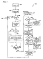
- the CRC stage 96a is entered only when the previous ME has indicated (via the next neighbor line 21a ( FIG. 2 )) that is has exited the stage. This ensures that the ME will access the most recent critical data (CRC residue). It is also critical that, throughout this pipe-stage, all threads execute in strict order to ensure that the CRC is calculated correctly. Because the CRC stage 96a uses the CAM 60, it firsts clears 202 the CAM of any data still in the CAM from a previous pipe-stage. It reads 204 the port type and determines 206 if it has been assigned an ATM cell. If the cell is not an ATM cell (that is, it is some other type, such as Ethernet or POS), the ME performing the CRC stage passes 208 the cell through without any processing. If the cell is an ATM cell, the ME 20 performs the CRC processing.
- the processing includes the following activities: reading the CRC residue, ATM type and SOP/EOP state in SRAM; determining if the cell is carrying an SOP, body or EOP; validating that the VC is carrying AAL5 cells and, if so, performing the CRC computation; and updating CRC residue and EOP-SOP status in SRAM.
- the CRC computation is performed using the CRC unit 72 ( FIG. 2 ) in the ME 20.
- the CRC computation must be performed in strict order to ensure that the CRC for cells that belong to the same VC are computed with the correct CRC residue.
- the CRC processing is divided into a read phase and a modify/write phase.
- the CAM 60 is used in both phases.
- the CAM 60 is used to decide whether a thread should read the residue/type fields from SRAM 38 or use the result from a previous thread stored in the Local Memory 66 ( FIG. 2 ).
- the first phase begins with a given thread searching the CAM 210 using the pointer to the re-assembly state. If the thread detects 212 a CAM miss, the thread writes 214 a CAM entry with the re-assembly pointer and state information to lock the entry, and issues a read to obtain the CRC residue and AAL type from SRAM memory 38. If, at 212, the thread detects a hit, it does not issue a read.
- the thread When the thread receives 216 the appropriate event signaling, that is, an event signal indicating that the previous thread has completed processing, the thread wakes and begins phase 2 processing. It searches 218 the CAM using the same re-assembly pointer. If the thread had issued a read and determines 220 a locked status for a matched CAM entry, the thread moves 222 the read result in the transfer registers to the local memory. The thread that moves the result also unlocks the entry, thereby ensuring a hit for future CAM lookups for that particular pointer. Otherwise, if the CAM entry is not locked, then a hit has occurred, and the thread simply reads 224 the corresponding information, that is, the residue and type, from the Local Memory.
- the appropriate event signaling that is, an event signal indicating that the previous thread has completed processing. It searches 218 the CAM using the same re-assembly pointer. If the thread had issued a read and determines 220 a locked status for a matched CAM entry, the
- each thread validates that the VC is carrying AAL5 by examining the type field from the VC table. For an AAL5 type, the thread computes 226 the CRC over the cell. If the type is not AAL5, the cell is handed off to an exception handler, or discarded, depending on the implementation.
- the thread determines 228 that the PTI bits in the ATM header indicate that the cell is an EOP cell
- the thread updates 230 the re-assembly state by setting the CRC residue to all zeroes and setting the SOP bit to a one. If the cell is not an EOP cell, the thread updates 232 the state with the new residue and sets SOP to zero. It saves 235 the updated CRC residue and SOP in the Local Memory for use by other threads and, according to its writeback cache policy, also writes the CRC residue and SOP back to the re-assembly state in the SRAM 38.
- the thread passes 236 the SOP, EOP and body status to the next (packet processing) stage.
- the CRC threads must use the EOP bit status provided in the header PTI field.
- the PTI bits only support EOP, so when an EOP is detected, the CRC thread sets an SOP bit in its section of the re-assembly state table indicating to the next thread that it has an SOP. Each time the CRC thread reads the re-assembly state, it reads the SOP bit, and if it is set, and the PTI bits in the ATM header indicate no EOP, it clears the SOP bit.
- the CRC thread Because other stages do not read the CRC threads re-assembly state area, the CRC thread also passes the EOP/SOP status down the pipeline. Once the CRC threads have completed the CRC calculation and the re-assembly state table is updated, the threads are ready to move onto the next pipe-stage.
- a thread When a thread completes its CRC calculation and issues its SRAM write of the residue/type, it also signals the thread of the next ME indicating that it can start its CRC pipe-stage. It is important that the signaling ensures that the next ME is not provided a signal until it can be assured that any pending residues will be written before the next ME issues its residue reads.
- the CAM 60 could be used to maintain coherency and correct packet processing sequence as well. For example, say threads are handling two successive packets that are in the same flow (or are associated with the same queue number) and access the same SRAM location. Because packet arrival rates are faster than SRAM access speeds, the thread handling the second packet will be ready to access the data before the SRAM read and modify activities of the thread handling the first (earlier) packet have completed. In this situation, the software-controlled CAM cache implementation can be used to recognize the dependency and to ensure that the most current information is always used. Thus, each thread uses the CAM 60 to do multiple compares in parallel using the CAM Lookup instruction, with a source register providing the flow number or queue number as the lookup value, as described earlier.
- the thread commences the SRAM read and allocates a CAM entry in into which the thread places the flow number. If the flow is already in the CAM, a hit indicator is returned along with a unique pointer value (for example, which entry number in the CAM matched).
- the thread that gets a hit in the CAM can obtain the latest copy of the data from local memory (cache in SRAM controller 40, or ME Local Memory 66) without having to do an SRAM read.
- a thread When a thread loads a flow number into a CAM entry, it also stores state information in the entry to enable subsequent thread lookups to determine that either a) the SRAM read has been started, but is not yet completed (it is "in-flight”); or b) the SRAM read has been completed, and the data is valid. If the "in-flight" status is determined, the subsequent thread knows that it should not start a read, but that it cannot yet use the read data. It can continue to test the status of the entry until it determines that the status has been changed to reflect valid data.
Landscapes
- Engineering & Computer Science (AREA)
- Theoretical Computer Science (AREA)
- Software Systems (AREA)
- Physics & Mathematics (AREA)
- General Engineering & Computer Science (AREA)
- General Physics & Mathematics (AREA)
- Memory System Of A Hierarchy Structure (AREA)
- Data Exchanges In Wide-Area Networks (AREA)
- Noise Elimination (AREA)
Description
- For maximum efficiency, network processors should be able to process packets at a rate at least equal to the line rate. Packet processing typically involves writes to and reads from external memory. Because of slower memory access speeds, current network processors may lack the necessary speed to process packets at the line speeds.
-
EP-A-0953897 describes a program-controlling processing unit which executes instructions stored in memory. A special instruction type is provided for selectively retrieving an element from memory in dependence on the value of input data subject of the instruction. Each instruction of this type has a header identifying the instruction type, and a body in the form of a hash table having at least one entry with both (i) a check value corresponding to a value of interest of the input data subject of the instruction, and (ii) an element to be used when the input data has said value of interest. Upon execution of such an instruction, the related input data is hashed to produce an offset value that is used to access in memory, relative to the position in memory of the current instruction, a corresponding entry in the hash table of the instruction. If a "hit " results (that is, the check value of the accessed entry matches the input data value), the entry element is operatively output. -
WO 01/48596 A -
WO 00/33195 A -
US-A-3806883 describes an arrangement for indicating which of N locations in a storage system was accessed least recently. The arrangement comprises storage registers equal in number to the number of addressable locations in an associated store of items, such as a content addressable memory, each of which holds one memory address. When a location in the store is accessed, its address is entered into the first address register and the content of all the registers up to but not including the one containing the accessed address are moved to the next register so that the registers contain a list of the order in which locations are accessed, the last register containing the address of the least recently used location.
According to the present invention there is provided a method, a computer program product and an apparatus as set forth in the claims. -
-
FIG. 1 is a block diagram of a communication system employing a processor having multithreaded microengines to support multiple threads of execution. -
FIG. 2 is a block diagram of a programmable processor datapath (of the microengine fromFIG. 1 ) that includes a CAM. -
FIG. 3 is a diagram depicting the microengines as a multi-stage, packet processing pipeline. -
FIG. 4 is a block diagram of the CAM ofFIG. 2 . -
FIG. 5A is a depiction of a queue and queue descriptor in SRAM memory. -
FIG. 5B is a depiction of a cache of queue descriptors and corresponding tag store implemented using the CAM (ofFIG. 4 ). -
FIG. 6 is a flow diagram illustrating an exemplary use of the CAM during a queue operation by one of the microengines programmed to perform queue management. -
FIG. 7 is a flow diagram illustrating an exemplary use of the CAM to support Cyclic Redundancy Check (CRC) processing by one of the pipeline microengines programmed to perform CRC processing. - Referring to
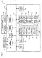
FIG. 1 , acommunication system 10 includes aprocessor 12 coupled to one or more I/O devices, for example,network devices memory system 18. Theprocessor 12 is multi-threaded processor and, as such, is especially useful for tasks that can be broken into parallel subtasks or functions. In one embodiment, as shown in the figure, theprocessor 12 includes multiple microengines 20, each with multiple hardware controlled program threads that can be simultaneously active and independently work on a task. In the example shown, there are sixteen microengines 20,microengines 20a-20p (corresponding tomicroengines 0 through 15), and each of the microengines 20 is capable of processing multiple program threads, as will be described more fully below. The maximum number of context threads supported in the illustrated embodiment is eight, but other maximum amount could be provided. Each of the microengines 20 is connected to and can communicate with adjacent microengines vianext neighbor lines 21, as shown. In the illustrated embodiment, the microengines 0-7 are organized as a first cluster (ME Cluster 0) 22a and the microengines 8-15 are organized as a second cluster (ME Cluster 1) 22b. - The
processor 12 also includes aprocessor 24 that assists in loading microcode control for other resources of theprocessor 12 and performs other general purpose computer type functions such as handling protocols and exceptions, as well as provides support for higher layer network processing tasks that cannot be handled by the microengines. In one embodiment, theprocessor 24 is a StrongARM (ARM is a trademark of ARM Limited, United Kingdom) core based architecture. The processor (or core) 24 has an operating system through which theprocessor 24 can call functions to operate on the microengines 20. Theprocessor 24 can use any supported operating system, preferably a real-time operating system. Other processor architectures may be used. - The microengines 20 each operate with shared resources including the
memory system 18, aPCI bus interface 26, an I/O interface 28, ahash unit 30 and ascratchpad memory 32. ThePCI bus interface 26 provides an interface to a PCI bus (not shown). The I/O interface 28 is responsible for controlling and interfacing theprocessor 12 to thenetwork devices memory system 18 includes a Dynamic Random Access Memory (DRAM) 34, which is accessed using aDRAM controller 36 and a Static Random Access Memory (SRAM) 38, which is accessed using anSRAM controller 40. Although not shown, theprocessor 12 also would include a nonvolatile memory to support boot operations. TheDRAM 34 andDRAM controller 36 are typically used for processing large volumes of data, e.g., processing of payloads from network packets. The SRAM 38 andSRAM controller 40 are used in a networking implementation for low latency, fast access tasks, e.g., accessing look-up tables, memory for theprocessor 24, and so forth. TheSRAM controller 40 includes a data structure (queue descriptor cache) and associated control logic to support efficient queue operations, as will be described in further detail later. Themicroengines 20a-20p can execute memory reference instructions to either theDRAM controller 36 or theSRAM controller 40. - The
devices network device 14 could be an Ethernet MAC device (connected to an Ethernet network, not shown) that transmits packet data to theprocessor 12 anddevice 16 could be a switch fabric device that receives processed packet data fromprocessor 12 for transmission onto a switch fabric. In such an implementation, that is, when handling traffic to be sent to a switch fabric, theprocessor 12 would be acting as an ingress network processor. Alternatively, theprocessor 12 could operate as an egress network processor, handling traffic that is received from a switch fabric (via device 16) and destined for another network device such asnetwork device 14, or network coupled to such device. Although theprocessor 12 can operate in a standalone mode, supporting both traffic directions, it will be understood that, to achieve higher performance, it may be desirable to use two dedicated processors, one as an ingress processor and the other as an egress processor. The two dedicated processors would each be coupled to thedevices network device processor 12. The I/O interface 28 therefore supports one or more types of interfaces, such as an interface for packet and cell transfer between a PHY device and a higher protocol layer (e.g., link layer), or an interface between a traffic manager and a switch fabric for Asynchronous Transfer Mode (ATM), Internet Protocol (IP), Ethernet, and similar data communications applications. The I/O interface 28 includes separate receive and transmit blocks, each being separately configurable for a particular interface supported by theprocessor 12. - Other devices, such as a host computer and/or PCI peripherals (not shown), which may be coupled to a PCI bus controlled by the
PC interface 26 are also serviced by theprocessor 12. - In general, as a network processor, the
processor 12 can interface to any type of communication device or interface that receives/sends large amounts of data. Theprocessor 12 functioning as a network processor could receive units of packet data from a network device likenetwork device 14 and process those units of packet data in a parallel manner, as will be described. The unit of packet data could include an entire network packet (e.g., Ethernet packet) or a portion of such a packet, e.g., a cell or packet segment. - Each of the functional units of the
processor 12 is coupled to aninternal bus structure 42.Memory busses memory controllers memory units DRAM 34 andSRAM 38 of thememory system 18. The I/O Interface 28 is coupled to thedevices O bus lines - Referring to
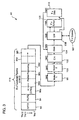
FIG. 2 , an exemplary one of themicroengines 20a is shown. The microengine (ME) 20a includes acontrol store 50 for storing a microprogram. The microprogram is loadable by theprocessor 24. - The
microengine 20a also includes anexecution datapath 54 and at least one general purpose register (GPR)file 56 that are coupled to thecontrol store 50. Thedatapath 54 includes several datapath elements, including anALU 58, amultiplier 59 and a Content Addressable Memory (CAM) 60. TheGPR file 56 provides operands to the various datapath processing elements including theCAM 60. Opcode bits in the instruction select which datapath element is to perform the operation defined by the instruction. - The
microengine 20a further includes a writetransfer register file 62 and a readtransfer register file 64. The writetransfer register file 62 stores data to be written to a resource external to the microengine (for example, the DRAM memory or SRAM memory). The readtransfer register file 64 is used for storing return data from a resource external to themicroengine 20a. Subsequent to or concurrent with the data arrival, an event signal from the respective shared resource, e.g.,memory controllers core 24, can be provided to alert the thread that the data is available or has been sent. Both of the transfer register files 62, 64 are connected to thedatapath 54, as well as thecontrol store 50. - Also included in the
microengine 20a is alocal memory 66. Thelocal memory 66 is addressed byregisters 68a, 68b, which supplies operands to thedatapath 54. Thelocal memory 66 receives results from thedatapath 54 as a destination. Themicroengine 20a also includes local control and status registers (CSRs) 70, coupled to the transfer registers, for storing local inter-thread and global event signaling information and other information, and aCRC unit 72, coupled to the transfer registers, which operates in parallel with theexecution datapath 54 and performs CRC computations for ATM cells. Themicroengine 20a also includes next neighbor registers 74, coupled to thecontrol store 50 and theexecution datapath 54, for storing information received from a previous neighbor ME in pipeline processing over a nextneighbor input signal 21a, or from the same ME, as controlled by information in thelocal CSRs 70. - In addition to providing an output to the
write transfer unit 62, the datapath can also provide an output to theGPR file 56 overline 80. Thus, each of the datapath elements, including theCAM 60 that can return a result value from an executed. A next neighbor output signal 21b to a next neighbor ME in the processing pipeline can be provided under the control of thelocal CSRs 80. - Other details of the microengine have been omitted for simplification. However, it will be appreciated that the microengine would include (and the
control store 50 would be coupled to) appropriate control hardware, such as program counters, instruction decode logic and context arbiter/event logic, needed to support multiple execution threads. - Referring to
FIG. 3 , an exemplary ME task assignment for a software pipeline model of theprocessor 12 is illustrated in 90. Theprocessor 12 supports two pipelines: a receive pipeline and a transmit pipeline. The receive pipeline includes the following stages: re-assembly pointer search ("RPTR") 92, re-assembly information update ("RUPD") 94, receive packet processing (six stages) 96a-96f, metering stages ME1 98 andME2 100, congestion avoidance ("CA") 102, statistics processing 104 and a queue manager ("QM") 106. The receive pipeline begins with data arriving in a receive block of the I/O interface 28 and ends with transmits queues 107 (stored in SRAM). The transmit pipeline stages include: aTX scheduler 108, theQM 106, a TransmitData stage 110 and the statistics processing 104. - The RPTR, RUPD and packet processing pipe stages work together to re-assemble segmented frames back into complete packets. The
RPTR stage 92 finds the pointer to the reassembly state information in theSRAM 38 and passes this pointer to theRUPD 98. TheRUPD 98 manages the reassembly state, which involves allocating DRAM buffers, and calculating offsets, byte counts and other variables, and provides the packet processing stage 96 with a pointer to the location in DRAM where the network data should be assembled. - The threads of the packet processing stages 96 complete the re-assembly process by writing the data (payload) to the allocated DRAM buffer and also look at the L2 through L7 packet headers to process the packet. These stages are application dependent and can therefore vary from one application to another. For example, one application may support IP destination searches to determine destination port, and a 7-tuple search to identify flows and support access lists.
- To support ATM re-assembly, the RX pipeline requires a cyclic redundancy code (CRC) stage in addition to the pipe stages already described. CRC support can be provided by replacing the first one of the packet processing stages (
stage 96a, as shown) and including additional information in the re-assembly state table. TheCRC 96a reads the re-assembly state to get the AAL type and CRC residue, verifies the Virtual Circuit (VC) is configured for AAL5, performs CRC calculation over the cell, and updates the CRC residue in the re-assembly state. -
Metering -
Congestion avoidance 102 monitors network traffic loads in an effort to anticipate and avoid congestion at common network bottlenecks. - The
QM 106 is responsible for performing enqueue and dequeue operations on the transmitqueues 107 for all packets, as will be described in further detail below. - The receive pipeline threads parse packet headers and perform lookups based on the packet header information. Once the packet has been processed, it is either sent as an exception to be further processed by the
core 24, or stored in theDRAM 34 and queued in a transmit queue by placing a packet link descriptor for it in a transmit queue associated with the transmit (forwarding port) indicated by the header/lookup. The transmit queue is stored in theSRAM 38. The transmit pipeline schedules packets for transmit data processing, which then sends the packet out onto the forwarding port indicated by the header/lookup information during the receive processing. - Collectively, the
stages threads 0 through 7) in each ME is assigned a single packet for processing. Consequently, at any one time there are 64 packets in the pipeline. Each stage executes at one packet arrival rate times execution period of eight threads. - The
stages - Some of the pipe stages, such as
CRC 96a,RUPD 94,QM 106, for example, operate on a "critical section" of code, that is, a code section for which only one ME thread has exclusive modification privileges for a global resource at any one time. These privileges protect coherency during read-modify-write operations. Exclusive modification privileges between MEs are handled by allowing only one ME (one stage) to modify the section. Thus, the architecture is designed to ensure that an ME not transition into a critical section stage until a previous ME has completed its processing in the critical section. For example, theRUPD 98 is a critical section that requires mutual exclusivity to shared tables in external memory. Thus, when transitioning fromRPTR 92 toRUPD 94,thread 0 of ME1 of theRUPD 94 will not begin until all threads on ME 0 having completed the previous RUPD pipe stage. In addition, strict thread order execution techniques are employed in the pipeline at critical section code points to ensure sequence management of packets being handled by the different threads. - The
processor 12 also supports the use of caching mechanisms to reduce packet processing times and improve the speed at which theprocessor 12 operates with respect to incoming traffic. For example, the SRAM controller 40 (FIG. 1 ) maintains a cache of most recently used queue descriptors (stored in the SRAM 38), as will be further described. Also, the local memory 66 (FIG. 2 ) caches CRC information, such as CRC residue (also stored in the SRAM) 38, used by theCRC 96a. If more than one thread in a pipe stage such as theQM 106 is required to modify the same critical data, a latency penalty is incurred if each thread reads the data from external memory (that is, SRAM), modifies it and writes the data back to external memory. To reduce the latency penalty associated with the read and write, the ME threads can use the ME CAM 60 (FIG. 2 ) to fold these operations into a single read, multiple modifications and, depending on the cache eviction policy, either one or more write operations, as will be described. -
FIG. 4 shows an exemplary embodiment of theCAM 60. TheCAM 60 includes a plurality ofentries 120. In the illustrated embodiment, there are 16 entries. Eachentry 120 has an identifier value (or tag) 122, e.g., a queue number or memory address that can be compared against an input lookup value. Each entry also includes anentry number 124 and state information 126 associated with theidentifier 122 in that same entry. Compareresults 128 are provided to a Status andLRU logic unit 130, which produces alookup result 132. Thelookup result 132 includes a hit/miss indicator 134,state information 136 and anentry number 138. Collectively, thefields status 140. - The width of the
identifiers 122 is the same as the source registers being used to provide load the CAM entries or provide lookup values, e.g., the registers of the GPR file 56 (FIG.·3). In the embodiment shown, the state information 126 is implemented as a state bit. The width and format of the state information, and the number of identifiers are based on design considerations. - During a CAM lookup operation, the value presented from a source such as the
GPR file 56 is compared, in parallel, to eachidentifier 122 with a resulting Match signal 142 per identifier. The values of each identifier were previously loaded by a CAM load operation. During that load operation, the values from theregister file 56 specified which of the identifiers and the values of the identifiers to be loaded. The state information is also loaded into the CAM during the CAM load operation. - The
identifier 122 is compared against the lookup value in a source operand by an instruction, e.g.,
Lookup[dest_reg, src_reg].
The source operand specified by the parameter "src_reg" holds the lookup value to be applied to theCAM 60 for lookup. The destination register specified by parameter "dest_reg" is the register that receives the result of theCAM lookup 60. - All
entries 120 are compared in parallel. In one embodiment, thelookup result 132 is a 6-bit value which is written into the specified destination register in bits 8:3, with the other bits of the register set to zero. The destination register can be a register in theGPR file 56. Optionally, thelookup result 132 can also be written into either of the LM_ADDR registers 68a, 68b (FIG. 2 ) of the ME 22. - For a hit (that is, when the hit/
miss indicator 134 of theresult 132 indicates a hit), theentry number 138 is the entry number of the entry that matched. When a miss occurs and the hit/miss indicator 134 thus indicates a miss, theentry number 138 is the entry number of the Least Recently-Used (LRU) entry in the CAM array. Thestate information 136 is only useful for a hit and includes the value in the state field 126 for the entry that hit. - The
LRU logic 130 maintains a time-ordered list of CAM entry usage. When an entry is loaded, or matches on a lookup, it is moved to a position of Most Recently Used (MRU), a lookup that misses does not modify the LRU list. - All applications can use the hit/
miss indication 134. Theentry number 138 andstate information 136 provide additional information that may be used by some applications. On a miss, for example, the LRU entry number can be used as a hint for cache eviction. The software is not required to use the hint. Thestate information 136 is information produced and used only by software. It can differentiate different meanings for a hit, such as unmodified versus modified data. The software can use the information for branch decisions, as offset into data tables, among other uses. - Other instructions that use and manage the CAM can include:
Write [entry, src_reg], opt_tok;
Write_State (state_value, entry) ;
Read_Tag (dest_reg, entry);
Read_State (dest_reg, entry); and
Clear.
The Write instruction writes an identifier value in the src_reg to the specified CAM entry. An option token can be used to specify state information. The Read_Tag and Read_State instructions are used for diagnostics, but can also be used in normal functions. The tag value and state for the specified entry are written into the destination register. Reading the tag is useful in the case where an entry needs to be evicted to make room for a new value-that is, the lookup of the new value results in a miss, with the LRU entry number returned as a result of the miss. The read instruction can then be used to find the value that is stored in that entry. The Read_Tag instruction eliminates the need to keep the identifier value corresponding to the LRU entry number in another register. The Clear instruction is used to flush all information out of the CAM. - When the CAM is used as a cache tag store, and each entry is associated with a block of data in
Local Memory 66, the result of the lookup can be used to branch on the hit/miss indicator 134 and use theentry number 138 as a base pointer into the block inLocal Memory 66. - In another embodiment, the state 126 can be implemented as a single lock bit and the
result 132 can be implemented to include a status code (instead of the separate indicator and state fields) along with theentry number 138. For example, the code could be defined as a two-bit code, with possible results to include a "miss" (code '01'), "hit" (code '10') and "locked" (code '11'). A return of the miss code would indicate that the lookup value is not in the CAM, and the entry number of the result value is the Least Recently Used (LRU) entry. As discussed above, this value could be used as a suggested entry to be replaced with the lookup value. A hit code would indicate that the lookup value is in the CAM and the lock bit is clear, with the entry number in the result being the entry number of the entry that has matched the lookup value. A locked code would indicate that the lookup value is in the CAM and the locked bit 126 is set, with the entry number that is provided in the result again being the entry number of the entry that matched the lookup value. - The lock bit 126 is a bit of data associated with the entry. The lock bit could be set or cleared by software, e.g., using a LOCK or UNLOCK instruction, at the time the entry is loaded, or changed in an already loaded entry. The lock bit 126 can be used to differentiate cases where the data associated with the CAM entry is in flight, or pending a change, as will be discussed in further detail later.
- As mentioned earlier, a context pipe stage that uses critical data is the only ME that uses that critical data. Therefore, the replacement policy for the CAM entries is to replace the LRU only on CAM misses. On the other hand, a functional pipeline (like the
pipeline 114 ofFIG. 3 ) performs the same function on multiple MEs. In a functional pipeline, therefore, a given ME is required to evict all critical data to external memory before it exits a stage that uses critical data and also must ensure that the CAM is cleared prior to any threads using the CAM. - Before a thread uses the critical data, it searches the CAM using a critical data identifier such as a memory address as a lookup value. As described earlier, the search results in one of three possibilities: a "miss", a "hit" or a "lock". If a miss is returned, then data is not saved locally. The thread reads the data from external memory (that is, from the SRAM 38) to replace the LRU data. It evicts LRU data from local memory (SRAM controller cache, or local memory 66) back to external memory, optionally locks the CAM entry and issues a read to get the new critical data from external memory. In certain applications, as will be described later, the lock is asserted to indicate to other threads that the data is in the process of being read into local memory, or to indicate to the same thread (the thread that initiated the read) that the memory read is still in progress. Once the critical data is returned, the thread awaiting the data processes the data, makes any modifications to the data, writes it to local memory, updates the entry from which LRU data was evicted with the new data and unlocks the CAM entry.
- If the result is a lock, the thread assumes that another ME thread is in the process of reading critical data and that it should not attempt to read the data. Instead, it tests the CAM at a later time and used the data when the lock is removed. When the result is a hit, then the critical data resides in local memory. Specific examples of CAM use will now be described with reference to
FIGS. 5 through 8 . - As discussed above, and as shown in
FIG. 3 , theprocessor 12 can be programmed to use one of the microengines 20 as theQM 106. TheCAM 60 in theQM 106 serves as a tag store holding the tags of queue descriptors that are cached by theSRAM controller 40. - The
QM 106 receives enqueue requests from the set of microengines functioning as the receivefunctional pipeline 114. The receivepipeline 114 is programmed to process and classify data packets received by one of thenetwork devices 14, 16 (FIG. 1 ), e.g., thephysical layer device 14. The enqueue requests specify which output queue an arriving packet should be sent to. The transmitscheduler 108 sends dequeue requests to theQM 106. The dequeue requests specify the output queue from which a packet is to be removed for transmittal to a destination via one of the network devices, 14, 16, e.g., theswitch fabric 16. - An enqueue operation adds information that arrived in a data packet to one of the output queues and updates the corresponding queue descriptor. A dequeue operation removes information from one of the output queues and updates the corresponding queue descriptor, thereby allowing the
network device 16 to transmit the information to the appropriate destination. - Referring to
FIG. 5A , an example of "n" transmitqueues 150 and theircorresponding queue descriptors 152 residing in external memory (SRAM 38) is shown. Eachoutput queue 150 includes a linked list ofelements 154, each of which has a pointer with the address of the next element in the queue. Eachelement 154 also includes a pointer that points to information that is stored elsewhere and that the element represents. Typically, the pointer of the last element in thequeue 150 contains a null value. Thequeue descriptor 152 includes an end ofpointer EOP indicator 156, asegment count 158, ahead pointer 160, atail pointer 162 and aframe count 164. Thedescriptor 152 may also include other queue parameters (not shown). Thehead pointer 160 points to the first element of the transmitqueue 150, and thetail pointer 30 points to the last element of the transmitqueue 150. Thesegment count 158 identifies the number of elements in the transmitqueue 150. - Referring now to
FIG. 5B , executing enqueue and dequeue operations for a large number of transmitqueues 150 in theSRAM memory 38 at high-bandwidth line rates can be accomplished by storing some of thequeue descriptors 152 in acache 170 in theSRAM controller 40. The ME 20 executing as thequeue manager 106 uses theidentifiers 122 of theentries 120 in itsCAM 60 to identify the memory addresses of the sixteenqueue descriptors 152 most-recently-used in enqueue or dequeue operations, that is, the cached queue descriptors. Thecache 170 stores the corresponding queue descriptors 152 (theEOP value 156, thesegment count 158, the head pointer160,tail pointer 162 and the frame count 164) stored at the addresses identified in the tag store (CAM 60). - The
queue manager 106 issues commands to returnqueue descriptors 152 tomemory 38 and fetchnew queue descriptors 152 from memory such that the queue descriptors stored in thecache 170 remain coherent with the addresses in thetag store 60. Thequeue manager 106 also issues commands to theSRAM controller 38 to indicate whichqueue descriptor 152 in thecache 170 should be used to execute the command. The commands that reference thehead pointer 160 ortail pointer 162 of aqueue descriptor 152 in thecache 170 are executed in the order in which they arrive at theSRAM controller 38. - Locating the
cache 170 ofqueue descriptors 152 at thememory controller 40 allows for low latency access to and from thecache 170 and thememory 38. Also, having the control structure for queue operations in a programming engine can allow for flexible high performance while using existing micro-engine hardware. - The threads associated with the
QM 106 execute in strict order. The threads use local inter-thread signaling to maintain strict order. To ensure that theQM 106 keeps up with in an incoming line rate, each thread performs one enqueue and one dequeue operation in a time slot equal to the minimum frame arrive time. -
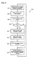
FIG. 6 illustrates an exemplary queue operation 180 (representing either an enqueue or dequeue operation) performed by theQM 106. TheQM 106 receives 182 a request for aqueue operation 182. The request is received from the CA content pipestage ME when it is an enqueue request and is received from the TX scheduler content pipe-stage ME when it is request for a dequeue operation. TheQM 106 reads 184 a queue number from the request. - The
QM 106 then uses its CAM to detect temporal dependencies between the queue specified in the request and the last 16 queues to which theQM 106 performed such an operation. Thus, theQM 106 performs aCAM lookup 186 based on the queue number identified in the request. If there is a dependency, i.e., the QM thread detects 188 a CAM hit, the latency of reading a queue descriptor is eliminated because the CAM hit indicates that the descriptor corresponding to the queue number is currently maintained in the queue descriptor cache 170 (FIG. 5B ). In the event that a hit occurs, theQM 106 proceeds to execute aninstruction 190 that commands theSRAM controller 40 to perform the requested operation. - If, at 188, it is determined that the CAM search results in a miss, the entry number of the least recently used CAM entry is returned to the
QM 106. There is a direct mapping between the CAM entry and a cache entry (queue descriptor). In other words, an LRU CAM entry "n" indicates that the cache entry "n" should be evicted. Therefore, theQM 106 evicts 192 from the cache the queue descriptor corresponding to the queue number stored in the LRU CAM entry. Once the cache entry is evicted, theQM 106 reads 194 the "new" queue descriptor (that is, the queue descriptor of the queue number in the request) into the cache from the SRAM. The new queue descriptor includes the linked list head pointer (for dequeue) and tail pointer (for enqueue), and a count that indicates the number of frames or buffers on the queue (as shown inFIGS. 5A-5B ). TheQM 106 also stores 196 the queue number of the new queue descriptor in the CAM entry that had been identified as the LRU entry to replace the number of the evicted queue descriptor. TheQM 106 executes aninstruction 190 that commands theSRAM controller 40 to perform the requested operation. - The
SRAM controller 40 performs the linked list operation for enqueue or dequeue. - When an operation of either type (enqueue or dequeue) is performed, the
QM 106 sends a message to theTX scheduler 108. After a dequeue operation, theQM 106 passes a transmit request to the TX data context pipe-stage 110. - Another stage that uses the
CAM 60 is the CRCprocessing pipe stage 96a. The ME 20 in this stage of the receivefunctional pipeline 114 uses itsinternal CAM 60 to maintain coherency of the CRC residue (in the re-assembly state table) between the eight threads executing the CRCprocessing pipe stage 96a. - Referring now to
FIG. 7a CRC pipe-stage program flow 200, including the use of theCAM 60 in support of the function is shown. TheCRC stage 96a is entered only when the previous ME has indicated (via thenext neighbor line 21a (FIG. 2 )) that is has exited the stage. This ensures that the ME will access the most recent critical data (CRC residue). It is also critical that, throughout this pipe-stage, all threads execute in strict order to ensure that the CRC is calculated correctly. Because theCRC stage 96a uses theCAM 60, it firsts clears 202 the CAM of any data still in the CAM from a previous pipe-stage. It reads 204 the port type and determines 206 if it has been assigned an ATM cell. If the cell is not an ATM cell (that is, it is some other type, such as Ethernet or POS), the ME performing the CRC stage passes 208 the cell through without any processing. If the cell is an ATM cell, the ME 20 performs the CRC processing. - The processing includes the following activities: reading the CRC residue, ATM type and SOP/EOP state in SRAM; determining if the cell is carrying an SOP, body or EOP; validating that the VC is carrying AAL5 cells and, if so, performing the CRC computation; and updating CRC residue and EOP-SOP status in SRAM.
- The CRC computation is performed using the CRC unit 72 (
FIG. 2 ) in the ME 20. The CRC computation must be performed in strict order to ensure that the CRC for cells that belong to the same VC are computed with the correct CRC residue. - The CRC processing is divided into a read phase and a modify/write phase. The
CAM 60 is used in both phases. In the first phase, theCAM 60 is used to decide whether a thread should read the residue/type fields fromSRAM 38 or use the result from a previous thread stored in the Local Memory 66 (FIG. 2 ). The first phase begins with a given thread searching theCAM 210 using the pointer to the re-assembly state. If the thread detects 212 a CAM miss, the thread writes 214 a CAM entry with the re-assembly pointer and state information to lock the entry, and issues a read to obtain the CRC residue and AAL type fromSRAM memory 38. If, at 212, the thread detects a hit, it does not issue a read. - When the thread receives 216 the appropriate event signaling, that is, an event signal indicating that the previous thread has completed processing, the thread wakes and begins
phase 2 processing. It searches 218 the CAM using the same re-assembly pointer. If the thread had issued a read and determines 220 a locked status for a matched CAM entry, the thread moves 222 the read result in the transfer registers to the local memory. The thread that moves the result also unlocks the entry, thereby ensuring a hit for future CAM lookups for that particular pointer. Otherwise, if the CAM entry is not locked, then a hit has occurred, and the thread simply reads 224 the corresponding information, that is, the residue and type, from the Local Memory. - After the second phase CAM search, each thread validates that the VC is carrying AAL5 by examining the type field from the VC table. For an AAL5 type, the thread computes 226 the CRC over the cell. If the type is not AAL5, the cell is handed off to an exception handler, or discarded, depending on the implementation.
- If the thread determines 228 that the PTI bits in the ATM header indicate that the cell is an EOP cell, the thread updates 230 the re-assembly state by setting the CRC residue to all zeroes and setting the SOP bit to a one. If the cell is not an EOP cell, the thread updates 232 the state with the new residue and sets SOP to zero. It saves 235 the updated CRC residue and SOP in the Local Memory for use by other threads and, according to its writeback cache policy, also writes the CRC residue and SOP back to the re-assembly state in the
SRAM 38. The thread passes 236 the SOP, EOP and body status to the next (packet processing) stage. - It is important that other stages in the RX pipeline know if the ATM cell contains an EOP, SOP or body. For ATM, the settings of the SOP and EOP bit indicate whether an entire cell was received (as opposed to an entire packet), so the CRC threads must use the EOP bit status provided in the header PTI field. The PTI bits only support EOP, so when an EOP is detected, the CRC thread sets an SOP bit in its section of the re-assembly state table indicating to the next thread that it has an SOP. Each time the CRC thread reads the re-assembly state, it reads the SOP bit, and if it is set, and the PTI bits in the ATM header indicate no EOP, it clears the SOP bit.
- Because other stages do not read the CRC threads re-assembly state area, the CRC thread also passes the EOP/SOP status down the pipeline. Once the CRC threads have completed the CRC calculation and the re-assembly state table is updated, the threads are ready to move onto the next pipe-stage.
- When a thread completes its CRC calculation and issues its SRAM write of the residue/type, it also signals the thread of the next ME indicating that it can start its CRC pipe-stage. It is important that the signaling ensures that the next ME is not provided a signal until it can be assured that any pending residues will be written before the next ME issues its residue reads.
- It will be understood that, while the implementation described thus far uses the
CAM 60 to reduce the number of read accesses (via "folding", as discussed earlier), the strict sequential ordering of the execution of context threads in a given stage is maintained not through the use of CAM, but instead by using local inter-thread signaling and by ensuring that read reference and modification activity completes before that same data in needed by successive threads. - It will be appreciated, however, that the
CAM 60 could be used to maintain coherency and correct packet processing sequence as well. For example, say threads are handling two successive packets that are in the same flow (or are associated with the same queue number) and access the same SRAM location. Because packet arrival rates are faster than SRAM access speeds, the thread handling the second packet will be ready to access the data before the SRAM read and modify activities of the thread handling the first (earlier) packet have completed. In this situation, the software-controlled CAM cache implementation can be used to recognize the dependency and to ensure that the most current information is always used. Thus, each thread uses theCAM 60 to do multiple compares in parallel using the CAM Lookup instruction, with a source register providing the flow number or queue number as the lookup value, as described earlier. - If a miss results, the thread commences the SRAM read and allocates a CAM entry in into which the thread places the flow number. If the flow is already in the CAM, a hit indicator is returned along with a unique pointer value (for example, which entry number in the CAM matched). The thread that gets a hit in the CAM can obtain the latest copy of the data from local memory (cache in
SRAM controller 40, or ME Local Memory 66) without having to do an SRAM read. - When a thread loads a flow number into a CAM entry, it also stores state information in the entry to enable subsequent thread lookups to determine that either a) the SRAM read has been started, but is not yet completed (it is "in-flight"); or b) the SRAM read has been completed, and the data is valid. If the "in-flight" status is determined, the subsequent thread knows that it should not start a read, but that it cannot yet use the read data. It can continue to test the status of the entry until it determines that the status has been changed to reflect valid data.
- Other embodiments are within the scope of the following claims.
Claims (9)
- A method of performing a data lookup comprising:providing an input value to a datapath element (58, 59, 60) disposed in an execution datapath (54) of a processor (12), wherein the datapath element comprises a content addressable memory CAM (60), wherein the CAM includes a plurality of entries that store identifier values and corresponding entry numbers, and wherein the CAM maintains a Least Recently Used (LRU) list of identifier values;causing the datapath element to compare the input value to stored identifier values; andreceiving from the datapath element a result based on the comparison, wherein the result includes status information indicating if a match is found, wherein the status information further includes an entry number, wherein the entry number corresponds to the matched identifier value if a match is indicated, and wherein, if the status information indicates that a match has not occurred as a result of the comparison, the entry number corresponds to the identifier value that is a LRU identifier value according to the list of LRU identifier values.
- The method of claim 1 wherein the status information further comprises status associated with the matched identifier value.
- The method of claim 2 wherein the identifier values are associated with data stored in a memory and the status comprises a lock status indicating that the data associated with the matched identifier value is in the process of being modified.
- The method of claim 1 wherein providing comprises executing an instruction having an operand that carries the input value.
- The method of claim 4 wherein the execution datapath (54) includes other datapath elements (58, 59, 60), and one or more bits in the instruction select the datapath element to perform an operation.
- The method of claim 1, wherein providing comprises executing a lookup instruction that specifies a source register to supply the operand carrying the input value and a destination register in which the result is to be stored.
- The method of claim 6 wherein the source and destination registers are registers in a general purpose register file coupled to the execution datapath (54).
- A computer program product residing on a computer- readable medium comprising instructions to cause a computer to perform the method of claim 1.
- An apparatus (10) comprising:a processor (12);a memory (18) storing a computer program product residing on a computer-readable medium comprising instructions to cause a computer to perform the method of claim 1.
Applications Claiming Priority (5)
| Application Number | Priority Date | Filing Date | Title |
|---|---|---|---|
| US31514401P | 2001-08-27 | 2001-08-27 | |
| US315144P | 2001-08-27 | ||
| US212943 | 2002-08-05 | ||
| US10/212,943 US6868476B2 (en) | 2001-08-27 | 2002-08-05 | Software controlled content addressable memory in a general purpose execution datapath |
| PCT/US2002/027354 WO2003019381A2 (en) | 2001-08-27 | 2002-08-27 | A software controlled content addressable memory in a general purpose execution datapath |
Publications (2)
| Publication Number | Publication Date |
|---|---|
| EP1586037A2 EP1586037A2 (en) | 2005-10-19 |
| EP1586037B1 true EP1586037B1 (en) | 2013-07-03 |
Family
ID=26907632
Family Applications (1)
| Application Number | Title | Priority Date | Filing Date |
|---|---|---|---|
| EP02768734.2A Expired - Lifetime EP1586037B1 (en) | 2001-08-27 | 2002-08-27 | A software controlled content addressable memory in a general purpose execution datapath |
Country Status (7)
| Country | Link |
|---|---|
| US (2) | US6868476B2 (en) |
| EP (1) | EP1586037B1 (en) |
| KR (1) | KR20040010789A (en) |
| AU (1) | AU2002331751A1 (en) |
| CA (1) | CA2456688A1 (en) |
| TW (1) | TWI228653B (en) |
| WO (1) | WO2003019381A2 (en) |
Families Citing this family (106)
| Publication number | Priority date | Publication date | Assignee | Title |
|---|---|---|---|---|
| US7266725B2 (en) | 2001-09-03 | 2007-09-04 | Pact Xpp Technologies Ag | Method for debugging reconfigurable architectures |
| DE19651075A1 (en) | 1996-12-09 | 1998-06-10 | Pact Inf Tech Gmbh | Unit for processing numerical and logical operations, for use in processors (CPU's), multi-computer systems, data flow processors (DFP's), digital signal processors (DSP's) or the like |
| DE19654595A1 (en) | 1996-12-20 | 1998-07-02 | Pact Inf Tech Gmbh | I0 and memory bus system for DFPs as well as building blocks with two- or multi-dimensional programmable cell structures |
| EP1329816B1 (en) | 1996-12-27 | 2011-06-22 | Richter, Thomas | Method for automatic dynamic unloading of data flow processors (dfp) as well as modules with bidimensional or multidimensional programmable cell structures (fpgas, dpgas or the like) |
| US6542998B1 (en) | 1997-02-08 | 2003-04-01 | Pact Gmbh | Method of self-synchronization of configurable elements of a programmable module |
| US8686549B2 (en) | 2001-09-03 | 2014-04-01 | Martin Vorbach | Reconfigurable elements |
| DE19861088A1 (en) | 1997-12-22 | 2000-02-10 | Pact Inf Tech Gmbh | Repairing integrated circuits by replacing subassemblies with substitutes |
| US7382736B2 (en) | 1999-01-12 | 2008-06-03 | Mcdata Corporation | Method for scoring queued frames for selective transmission through a switch |
| JP2003505753A (en) | 1999-06-10 | 2003-02-12 | ペーアーツェーテー インフォルマツィオーンステヒノロギー ゲゼルシャフト ミット ベシュレンクテル ハフツング | Sequence division method in cell structure |
| JP2004506261A (en) | 2000-06-13 | 2004-02-26 | ペーアーツェーテー イクスペーペー テクノロジーズ アクチエンゲゼルシャフト | Pipeline CT protocol and CT communication |
| AU2002220600A1 (en) * | 2000-10-06 | 2002-04-15 | Pact Informationstechnologie Gmbh | Cell system with segmented intermediate cell structure |
| US8058899B2 (en) | 2000-10-06 | 2011-11-15 | Martin Vorbach | Logic cell array and bus system |
| US7236490B2 (en) * | 2000-11-17 | 2007-06-26 | Foundry Networks, Inc. | Backplane interface adapter |
| US7596139B2 (en) | 2000-11-17 | 2009-09-29 | Foundry Networks, Inc. | Backplane interface adapter with error control and redundant fabric |
| US7002980B1 (en) | 2000-12-19 | 2006-02-21 | Chiaro Networks, Ltd. | System and method for router queue and congestion management |
| US7844796B2 (en) * | 2001-03-05 | 2010-11-30 | Martin Vorbach | Data processing device and method |
| US9037807B2 (en) | 2001-03-05 | 2015-05-19 | Pact Xpp Technologies Ag | Processor arrangement on a chip including data processing, memory, and interface elements |
| US7581076B2 (en) * | 2001-03-05 | 2009-08-25 | Pact Xpp Technologies Ag | Methods and devices for treating and/or processing data |
| US7444531B2 (en) | 2001-03-05 | 2008-10-28 | Pact Xpp Technologies Ag | Methods and devices for treating and processing data |
| US20070299993A1 (en) * | 2001-03-05 | 2007-12-27 | Pact Xpp Technologies Ag | Method and Device for Treating and Processing Data |
| US9436631B2 (en) | 2001-03-05 | 2016-09-06 | Pact Xpp Technologies Ag | Chip including memory element storing higher level memory data on a page by page basis |
| US9552047B2 (en) | 2001-03-05 | 2017-01-24 | Pact Xpp Technologies Ag | Multiprocessor having runtime adjustable clock and clock dependent power supply |
| US9411532B2 (en) | 2001-09-07 | 2016-08-09 | Pact Xpp Technologies Ag | Methods and systems for transferring data between a processing device and external devices |
| JP2004533691A (en) | 2001-06-20 | 2004-11-04 | ペーアーツェーテー イクスペーペー テクノロジーズ アクチエンゲゼルシャフト | Methods for processing data |
| US7996827B2 (en) | 2001-08-16 | 2011-08-09 | Martin Vorbach | Method for the translation of programs for reconfigurable architectures |
| US7216204B2 (en) * | 2001-08-27 | 2007-05-08 | Intel Corporation | Mechanism for providing early coherency detection to enable high performance memory updates in a latency sensitive multithreaded environment |
| US7225281B2 (en) * | 2001-08-27 | 2007-05-29 | Intel Corporation | Multiprocessor infrastructure for providing flexible bandwidth allocation via multiple instantiations of separate data buses, control buses and support mechanisms |
| US6868476B2 (en) * | 2001-08-27 | 2005-03-15 | Intel Corporation | Software controlled content addressable memory in a general purpose execution datapath |
| US7487505B2 (en) * | 2001-08-27 | 2009-02-03 | Intel Corporation | Multithreaded microprocessor with register allocation based on number of active threads |
| US7434191B2 (en) | 2001-09-03 | 2008-10-07 | Pact Xpp Technologies Ag | Router |
| US8686475B2 (en) | 2001-09-19 | 2014-04-01 | Pact Xpp Technologies Ag | Reconfigurable elements |
| US7107413B2 (en) * | 2001-12-17 | 2006-09-12 | Intel Corporation | Write queue descriptor count instruction for high speed queuing |
| US7269179B2 (en) * | 2001-12-18 | 2007-09-11 | Intel Corporation | Control mechanisms for enqueue and dequeue operations in a pipelined network processor |
| US7895239B2 (en) | 2002-01-04 | 2011-02-22 | Intel Corporation | Queue arrays in network devices |
| US7181573B2 (en) * | 2002-01-07 | 2007-02-20 | Intel Corporation | Queue array caching in network devices |
| US6934951B2 (en) * | 2002-01-17 | 2005-08-23 | Intel Corporation | Parallel processor with functional pipeline providing programming engines by supporting multiple contexts and critical section |
| US8281108B2 (en) | 2002-01-19 | 2012-10-02 | Martin Vorbach | Reconfigurable general purpose processor having time restricted configurations |
| US7610451B2 (en) * | 2002-01-25 | 2009-10-27 | Intel Corporation | Data transfer mechanism using unidirectional pull bus and push bus |
| US7149226B2 (en) * | 2002-02-01 | 2006-12-12 | Intel Corporation | Processing data packets |
| US8127061B2 (en) | 2002-02-18 | 2012-02-28 | Martin Vorbach | Bus systems and reconfiguration methods |
| US8914590B2 (en) | 2002-08-07 | 2014-12-16 | Pact Xpp Technologies Ag | Data processing method and device |
| US9170812B2 (en) | 2002-03-21 | 2015-10-27 | Pact Xpp Technologies Ag | Data processing system having integrated pipelined array data processor |
| US20070079077A1 (en) * | 2002-04-29 | 2007-04-05 | Baines Mandeep S | System, method, and computer program product for shared memory queue |
| US7266117B1 (en) | 2002-05-06 | 2007-09-04 | Foundry Networks, Inc. | System architecture for very fast ethernet blade |
| US7649885B1 (en) | 2002-05-06 | 2010-01-19 | Foundry Networks, Inc. | Network routing system for enhanced efficiency and monitoring capability |
| US20120155466A1 (en) | 2002-05-06 | 2012-06-21 | Ian Edward Davis | Method and apparatus for efficiently processing data packets in a computer network |
| US7468975B1 (en) | 2002-05-06 | 2008-12-23 | Foundry Networks, Inc. | Flexible method for processing data packets in a network routing system for enhanced efficiency and monitoring capability |
| US7187687B1 (en) | 2002-05-06 | 2007-03-06 | Foundry Networks, Inc. | Pipeline method and system for switching packets |
| US7320037B1 (en) | 2002-05-10 | 2008-01-15 | Altera Corporation | Method and apparatus for packet segmentation, enqueuing and queue servicing for multiple network processor architecture |
| US7593334B1 (en) | 2002-05-20 | 2009-09-22 | Altera Corporation | Method of policing network traffic |
| US7336669B1 (en) | 2002-05-20 | 2008-02-26 | Altera Corporation | Mechanism for distributing statistics across multiple elements |
| US7657861B2 (en) | 2002-08-07 | 2010-02-02 | Pact Xpp Technologies Ag | Method and device for processing data |
| WO2004021176A2 (en) | 2002-08-07 | 2004-03-11 | Pact Xpp Technologies Ag | Method and device for processing data |
| US7337275B2 (en) * | 2002-08-13 | 2008-02-26 | Intel Corporation | Free list and ring data structure management |
| EP1537486A1 (en) | 2002-09-06 | 2005-06-08 | PACT XPP Technologies AG | Reconfigurable sequencer structure |
| US7415540B2 (en) * | 2002-12-31 | 2008-08-19 | Intel Corporation | Scheduling processing threads |
| US6941438B2 (en) * | 2003-01-10 | 2005-09-06 | Intel Corporation | Memory interleaving |
| US6901072B1 (en) | 2003-05-15 | 2005-05-31 | Foundry Networks, Inc. | System and method for high speed packet transmission implementing dual transmit and receive pipelines |
| US7500239B2 (en) * | 2003-05-23 | 2009-03-03 | Intel Corporation | Packet processing system |
| EP1634182A2 (en) * | 2003-06-17 | 2006-03-15 | PACT XPP Technologies AG | Data processing device and method |
| US7240164B2 (en) * | 2003-08-14 | 2007-07-03 | Intel Corporation | Folding for a multi-threaded network processor |
| JP4700611B2 (en) * | 2003-08-28 | 2011-06-15 | ペーアーツェーテー イクスペーペー テクノロジーズ アクチエンゲゼルシャフト | Data processing apparatus and data processing method |
| US7213099B2 (en) * | 2003-12-30 | 2007-05-01 | Intel Corporation | Method and apparatus utilizing non-uniformly distributed DRAM configurations and to detect in-range memory address matches |
| US20050216655A1 (en) * | 2004-03-25 | 2005-09-29 | Rosenbluth Mark B | Content addressable memory constructed from random access memory |
| US7181568B2 (en) * | 2004-03-25 | 2007-02-20 | Intel Corporation | Content addressable memory to identify subtag matches |
| US7817659B2 (en) | 2004-03-26 | 2010-10-19 | Foundry Networks, Llc | Method and apparatus for aggregating input data streams |
| US7719540B2 (en) * | 2004-03-31 | 2010-05-18 | Intel Corporation | Render-cache controller for multithreading, multi-core graphics processor |
| US8730961B1 (en) | 2004-04-26 | 2014-05-20 | Foundry Networks, Llc | System and method for optimizing router lookup |
| US7418540B2 (en) * | 2004-04-28 | 2008-08-26 | Intel Corporation | Memory controller with command queue look-ahead |
| US7599361B2 (en) * | 2004-07-02 | 2009-10-06 | P-Cube Ltd. | Wire-speed packet management in a multi-pipeline network processor |
| US20060067348A1 (en) * | 2004-09-30 | 2006-03-30 | Sanjeev Jain | System and method for efficient memory access of queue control data structures |
| US7657703B1 (en) | 2004-10-29 | 2010-02-02 | Foundry Networks, Inc. | Double density content addressable memory (CAM) lookup scheme |
| US7401184B2 (en) * | 2004-11-19 | 2008-07-15 | Intel Corporation | Matching memory transactions to cache line boundaries |
| US7555630B2 (en) * | 2004-12-21 | 2009-06-30 | Intel Corporation | Method and apparatus to provide efficient communication between multi-threaded processing elements in a processor unit |
| US7467256B2 (en) * | 2004-12-28 | 2008-12-16 | Intel Corporation | Processor having content addressable memory for block-based queue structures |
| US20060140203A1 (en) * | 2004-12-28 | 2006-06-29 | Sanjeev Jain | System and method for packet queuing |
| US8762595B1 (en) * | 2005-04-05 | 2014-06-24 | Oracle America, Inc. | Method for sharing interfaces among multiple domain environments with enhanced hooks for exclusiveness |
| US7793040B2 (en) | 2005-06-01 | 2010-09-07 | Microsoft Corporation | Content addressable memory architecture |
| US7451297B2 (en) | 2005-06-01 | 2008-11-11 | Microsoft Corporation | Computing system and method that determines current configuration dependent on operand input from another configuration |
| US7707387B2 (en) * | 2005-06-01 | 2010-04-27 | Microsoft Corporation | Conditional execution via content addressable memory and parallel computing execution model |
| US7853951B2 (en) * | 2005-07-25 | 2010-12-14 | Intel Corporation | Lock sequencing to reorder and grant lock requests from multiple program threads |
| US20070044103A1 (en) * | 2005-07-25 | 2007-02-22 | Mark Rosenbluth | Inter-thread communication of lock protected data |
| DE112006002237B4 (en) * | 2005-08-23 | 2023-04-06 | Advanced Micro Devices, Inc. | Method for self-initiating synchronization in a computer system |
| US20070124728A1 (en) * | 2005-11-28 | 2007-05-31 | Mark Rosenbluth | Passing work between threads |
| US7624250B2 (en) | 2005-12-05 | 2009-11-24 | Intel Corporation | Heterogeneous multi-core processor having dedicated connections between processor cores |
| US7593971B1 (en) * | 2005-12-07 | 2009-09-22 | Nvidia Corporation | Configurable state table for managing multiple versions of state information |
| US8448162B2 (en) | 2005-12-28 | 2013-05-21 | Foundry Networks, Llc | Hitless software upgrades |
| US20070157030A1 (en) * | 2005-12-30 | 2007-07-05 | Feghali Wajdi K | Cryptographic system component |
| JP2009524134A (en) * | 2006-01-18 | 2009-06-25 | ペーアーツェーテー イクスペーペー テクノロジーズ アクチエンゲゼルシャフト | Hardware definition method |
| US7903654B2 (en) | 2006-08-22 | 2011-03-08 | Foundry Networks, Llc | System and method for ECMP load sharing |
| US8238255B2 (en) | 2006-11-22 | 2012-08-07 | Foundry Networks, Llc | Recovering from failures without impact on data traffic in a shared bus architecture |
| US8127113B1 (en) | 2006-12-01 | 2012-02-28 | Synopsys, Inc. | Generating hardware accelerators and processor offloads |
| US8289966B1 (en) | 2006-12-01 | 2012-10-16 | Synopsys, Inc. | Packet ingress/egress block and system and method for receiving, transmitting, and managing packetized data |
| US8706987B1 (en) | 2006-12-01 | 2014-04-22 | Synopsys, Inc. | Structured block transfer module, system architecture, and method for transferring |
| US7978614B2 (en) | 2007-01-11 | 2011-07-12 | Foundry Network, LLC | Techniques for detecting non-receipt of fault detection protocol packets |
| US9601199B2 (en) | 2007-01-26 | 2017-03-21 | Intel Corporation | Iterator register for structured memory |
| TWI499909B (en) | 2007-01-26 | 2015-09-11 | Cheriton David | Hierarchical immutable content-addressable memory processor |
| US8271859B2 (en) | 2007-07-18 | 2012-09-18 | Foundry Networks Llc | Segmented CRC design in high speed networks |
| US8037399B2 (en) | 2007-07-18 | 2011-10-11 | Foundry Networks, Llc | Techniques for segmented CRC design in high speed networks |
| US8509236B2 (en) | 2007-09-26 | 2013-08-13 | Foundry Networks, Llc | Techniques for selecting paths and/or trunk ports for forwarding traffic flows |
| US7921195B2 (en) * | 2008-06-09 | 2011-04-05 | International Business Machines Corporation | Optimizing service processing based on business information, operational intelligence, and self-learning |
| US8090901B2 (en) | 2009-05-14 | 2012-01-03 | Brocade Communications Systems, Inc. | TCAM management approach that minimize movements |
| US8599850B2 (en) | 2009-09-21 | 2013-12-03 | Brocade Communications Systems, Inc. | Provisioning single or multistage networks using ethernet service instances (ESIs) |
| US9009401B2 (en) * | 2012-07-27 | 2015-04-14 | International Business Machines Corporation | Multi-updatable least recently used mechanism |
| US10867642B2 (en) | 2016-05-17 | 2020-12-15 | Taiwan Semiconductor Manufacturing Company Limited | Active random access memory |
| US11237960B2 (en) * | 2019-05-21 | 2022-02-01 | Arm Limited | Method and apparatus for asynchronous memory write-back in a data processing system |
Family Cites Families (221)
| Publication number | Priority date | Publication date | Assignee | Title |
|---|---|---|---|---|
| US557766A (en) * | 1896-04-07 | Collar-creasing machine | ||
| US3373408A (en) | 1965-04-16 | 1968-03-12 | Rca Corp | Computer capable of switching between programs without storage and retrieval of the contents of operation registers |
| US3478322A (en) | 1967-05-23 | 1969-11-11 | Ibm | Data processor employing electronically changeable control storage |
| BE795789A (en) | 1972-03-08 | 1973-06-18 | Burroughs Corp | MICROPROGRAM CONTAINING A MICRO-RECOVERY INSTRUCTION |
| US3881173A (en) | 1973-05-14 | 1975-04-29 | Amdahl Corp | Condition code determination and data processing |
| IT986411B (en) | 1973-06-05 | 1975-01-30 | Olivetti E C Spa | SYSTEM TO TRANSFER THE CONTROL OF PROCESSING FROM A FIRST PRIORITY LEVEL TO A SECOND PRIORITY LEVEL |
| FR2253415A5 (en) | 1973-12-04 | 1975-06-27 | Cii | |
| US3913074A (en) | 1973-12-18 | 1975-10-14 | Honeywell Inf Systems | Search processing apparatus |
| US4045782A (en) | 1976-03-29 | 1977-08-30 | The Warner & Swasey Company | Microprogrammed processor system having external memory |
| US4130890A (en) | 1977-06-08 | 1978-12-19 | Itt Industries, Inc. | Integrated DDC memory with bitwise erase |
| US4392758A (en) | 1978-05-22 | 1983-07-12 | International Business Machines Corporation | Underscore erase |
| US4189767A (en) * | 1978-06-05 | 1980-02-19 | Bell Telephone Laboratories, Incorporated | Accessing arrangement for interleaved modular memories |
| JPS56164464A (en) | 1980-05-21 | 1981-12-17 | Tatsuo Nogi | Parallel processing computer |
| US4400770A (en) | 1980-11-10 | 1983-08-23 | International Business Machines Corporation | Cache synonym detection and handling means |
| CA1179069A (en) | 1981-04-10 | 1984-12-04 | Yasushi Fukunaga | Data transmission apparatus for a multiprocessor system |
| US4517807A (en) * | 1982-09-10 | 1985-05-21 | Borg-Warner Corporation | Heat pump water heater with supplemental heat supply |
| US4569016A (en) | 1983-06-30 | 1986-02-04 | International Business Machines Corporation | Mechanism for implementing one machine cycle executable mask and rotate instructions in a primitive instruction set computing system |
| US4868735A (en) | 1984-05-08 | 1989-09-19 | Advanced Micro Devices, Inc. | Interruptible structured microprogrammed sixteen-bit address sequence controller |
| US4742451A (en) | 1984-05-21 | 1988-05-03 | Digital Equipment Corporation | Instruction prefetch system for conditional branch instruction for central processor unit |
| US4777587A (en) | 1985-08-30 | 1988-10-11 | Advanced Micro Devices, Inc. | System for processing single-cycle branch instruction in a pipeline having relative, absolute, indirect and trap addresses |
| JPS62103893A (en) * | 1985-10-30 | 1987-05-14 | Toshiba Corp | Semiconductor memory |
| US5021945A (en) | 1985-10-31 | 1991-06-04 | Mcc Development, Ltd. | Parallel processor system for processing natural concurrencies and method therefor |
| US4745544A (en) | 1985-12-12 | 1988-05-17 | Texas Instruments Incorporated | Master/slave sequencing processor with forced I/O |
| US4724521A (en) | 1986-01-14 | 1988-02-09 | Veri-Fone, Inc. | Method for operating a local terminal to execute a downloaded application program |
| US5297260A (en) | 1986-03-12 | 1994-03-22 | Hitachi, Ltd. | Processor having a plurality of CPUS with one CPU being normally connected to common bus |
| US4992934A (en) | 1986-12-15 | 1991-02-12 | United Technologies Corporation | Reduced instruction set computing apparatus and methods |
| US5073864A (en) | 1987-02-10 | 1991-12-17 | Davin Computer Corporation | Parallel string processor and method for a minicomputer |
| US4866664A (en) | 1987-03-09 | 1989-09-12 | Unisys Corporation | Intercomputer communication control apparatus & method |
| US5142683A (en) | 1987-03-09 | 1992-08-25 | Unisys Corporation | Intercomputer communication control apparatus and method |
| EP0357768B1 (en) | 1988-03-14 | 1994-03-09 | Unisys Corporation | Record lock processor for multiprocessing data system |
| US5008808A (en) * | 1988-06-23 | 1991-04-16 | Storage Technology Corporation | Consolidation of commands in a buffered input/output device |
| US5165025A (en) | 1988-10-06 | 1992-11-17 | Lass Stanley E | Interlacing the paths after a conditional branch like instruction |
| US5142676A (en) * | 1988-12-28 | 1992-08-25 | Gte Laboratories Incorporated | Separate content addressable memories for storing locked segment addresses and locking processor identifications for controlling access to shared memory |
| US5155854A (en) | 1989-02-03 | 1992-10-13 | Digital Equipment Corporation | System for arbitrating communication requests using multi-pass control unit based on availability of system resources |
| US5155831A (en) | 1989-04-24 | 1992-10-13 | International Business Machines Corporation | Data processing system with fast queue store interposed between store-through caches and a main memory |
| US5166872A (en) | 1989-07-17 | 1992-11-24 | Ability Technologies Corporation | System and method for controlling devices through communication processors and pluralities of address-associated device controllers sharing each communication processor |
| US5113516A (en) | 1989-07-31 | 1992-05-12 | North American Philips Corporation | Data repacker having controlled feedback shifters and registers for changing data format |
| US5168555A (en) | 1989-09-06 | 1992-12-01 | Unisys Corporation | Initial program load control |
| US5263169A (en) | 1989-11-03 | 1993-11-16 | Zoran Corporation | Bus arbitration and resource management for concurrent vector signal processor architecture |
| DE3942977A1 (en) | 1989-12-23 | 1991-06-27 | Standard Elektrik Lorenz Ag | METHOD FOR RESTORING THE CORRECT SEQUENCE OF CELLS, ESPECIALLY IN AN ATM SWITCHING CENTER, AND OUTPUT UNIT THEREFOR |
| US5179702A (en) * | 1989-12-29 | 1993-01-12 | Supercomputer Systems Limited Partnership | System and method for controlling a highly parallel multiprocessor using an anarchy based scheduler for parallel execution thread scheduling |
| US5247671A (en) | 1990-02-14 | 1993-09-21 | International Business Machines Corporation | Scalable schedules for serial communications controller in data processing systems |
| EP0446721B1 (en) | 1990-03-16 | 2000-12-20 | Texas Instruments Incorporated | Distributed processing memory |
| JPH0799812B2 (en) | 1990-03-26 | 1995-10-25 | 株式会社グラフイックス・コミュニケーション・テクノロジーズ | Signal coding apparatus, signal decoding apparatus, and signal coding / decoding apparatus |
| EP0449369B1 (en) | 1990-03-27 | 1998-07-29 | Koninklijke Philips Electronics N.V. | A data processing system provided with a performance enhancing instruction cache |
| US5390329A (en) | 1990-06-11 | 1995-02-14 | Cray Research, Inc. | Responding to service requests using minimal system-side context in a multiprocessor environment |
| US5404482A (en) | 1990-06-29 | 1995-04-04 | Digital Equipment Corporation | Processor and method for preventing access to a locked memory block by recording a lock in a content addressable memory with outstanding cache fills |
| US5432918A (en) | 1990-06-29 | 1995-07-11 | Digital Equipment Corporation | Method and apparatus for ordering read and write operations using conflict bits in a write queue |
| US5347648A (en) | 1990-06-29 | 1994-09-13 | Digital Equipment Corporation | Ensuring write ordering under writeback cache error conditions |
| AU630299B2 (en) | 1990-07-10 | 1992-10-22 | Fujitsu Limited | A data gathering/scattering system in a parallel computer |
| US5367678A (en) | 1990-12-06 | 1994-11-22 | The Regents Of The University Of California | Multiprocessor system having statically determining resource allocation schedule at compile time and the using of static schedule with processor signals to control the execution time dynamically |
| KR960001273B1 (en) * | 1991-04-30 | 1996-01-25 | 가부시키가이샤 도시바 | Single chip microcomputer |
| EP0522513A2 (en) | 1991-07-09 | 1993-01-13 | Hughes Aircraft Company | High speed parallel microcode program controller |
| US5255239A (en) | 1991-08-13 | 1993-10-19 | Cypress Semiconductor Corporation | Bidirectional first-in-first-out memory device with transparent and user-testable capabilities |
| US5623489A (en) | 1991-09-26 | 1997-04-22 | Ipc Information Systems, Inc. | Channel allocation system for distributed digital switching network |
| US5392412A (en) | 1991-10-03 | 1995-02-21 | Standard Microsystems Corporation | Data communication controller for use with a single-port data packet buffer |
| GB2260429B (en) | 1991-10-11 | 1995-05-24 | Intel Corp | Versatile cache memory |
| US5392391A (en) | 1991-10-18 | 1995-02-21 | Lsi Logic Corporation | High performance graphics applications controller |
| DE69231957T2 (en) | 1991-10-21 | 2002-04-04 | Toshiba Kawasaki Kk | High speed processor capable of handling multiple interruptions |
| US5452437A (en) | 1991-11-18 | 1995-09-19 | Motorola, Inc. | Methods of debugging multiprocessor system |
| US5357617A (en) | 1991-11-22 | 1994-10-18 | International Business Machines Corporation | Method and apparatus for substantially concurrent multiple instruction thread processing by a single pipeline processor |
| US5442797A (en) | 1991-12-04 | 1995-08-15 | Casavant; Thomas L. | Latency tolerant risc-based multiple processor with event driven locality managers resulting from variable tagging |
| JP2823767B2 (en) | 1992-02-03 | 1998-11-11 | 松下電器産業株式会社 | Register file |
| US5459842A (en) | 1992-06-26 | 1995-10-17 | International Business Machines Corporation | System for combining data from multiple CPU write requests via buffers and using read-modify-write operation to write the combined data to the memory |
| DE4223600C2 (en) | 1992-07-17 | 1994-10-13 | Ibm | Multiprocessor computer system and method for transmitting control information and data information between at least two processor units of a computer system |
| US5274770A (en) | 1992-07-29 | 1993-12-28 | Tritech Microelectronics International Pte Ltd. | Flexible register-based I/O microcontroller with single cycle instruction execution |
| US5692167A (en) | 1992-07-31 | 1997-11-25 | Intel Corporation | Method for verifying the correct processing of pipelined instructions including branch instructions and self-modifying code in a microprocessor |
| US5442756A (en) | 1992-07-31 | 1995-08-15 | Intel Corporation | Branch prediction and resolution apparatus for a superscalar computer processor |
| US5649109A (en) | 1992-10-22 | 1997-07-15 | Digital Equipment Corporation | Apparatus and method for maintaining forwarding information in a bridge or router using multiple free queues having associated free space sizes |
| US5481683A (en) | 1992-10-30 | 1996-01-02 | International Business Machines Corporation | Super scalar computer architecture using remand and recycled general purpose register to manage out-of-order execution of instructions |
| US5450603A (en) | 1992-12-18 | 1995-09-12 | Xerox Corporation | SIMD architecture with transfer register or value source circuitry connected to bus |
| JP3776449B2 (en) | 1992-12-23 | 2006-05-17 | セントル エレクトロニク オルロジェール ソシエテ アノニム | Multitasking low power controller |
| US5404464A (en) | 1993-02-11 | 1995-04-04 | Ast Research, Inc. | Bus control system and method that selectively generate an early address strobe |
| US5448702A (en) | 1993-03-02 | 1995-09-05 | International Business Machines Corporation | Adapters with descriptor queue management capability |
| EP0617361B1 (en) * | 1993-03-26 | 2001-11-28 | Cabletron Systems, Inc. | Scheduling method and apparatus for a communication network |
| US5522069A (en) | 1993-04-30 | 1996-05-28 | Zenith Data Systems Corporation | Symmetric multiprocessing system with unified environment and distributed system functions |
| WO1994027216A1 (en) | 1993-05-14 | 1994-11-24 | Massachusetts Institute Of Technology | Multiprocessor coupling system with integrated compile and run time scheduling for parallelism |
| CA2122182A1 (en) | 1993-05-20 | 1994-11-21 | Rene Leblanc | Method for rapid prototyping of programming problems |
| US5363448A (en) | 1993-06-30 | 1994-11-08 | United Technologies Automotive, Inc. | Pseudorandom number generation and cryptographic authentication |
| CA2107299C (en) | 1993-09-29 | 1997-02-25 | Mehrad Yasrebi | High performance machine for switched communications in a heterogenous data processing network gateway |
| US5446736A (en) | 1993-10-07 | 1995-08-29 | Ast Research, Inc. | Method and apparatus for connecting a node to a wireless network using a standard protocol |
| US5450351A (en) | 1993-11-19 | 1995-09-12 | International Business Machines Corporation | Content addressable memory implementation with random access memory |
| JP3169155B2 (en) * | 1993-12-22 | 2001-05-21 | インターナショナル・ビジネス・マシーンズ・コーポレ−ション | Circuit for caching information |
| US5487159A (en) | 1993-12-23 | 1996-01-23 | Unisys Corporation | System for processing shift, mask, and merge operations in one instruction |
| US5490204A (en) | 1994-03-01 | 1996-02-06 | Safco Corporation | Automated quality assessment system for cellular networks |
| US5835755A (en) | 1994-04-04 | 1998-11-10 | At&T Global Information Solutions Company | Multi-processor computer system for operating parallel client/server database processes |
| JP3547482B2 (en) | 1994-04-15 | 2004-07-28 | 株式会社日立製作所 | Information processing equipment |
| US5659722A (en) | 1994-04-28 | 1997-08-19 | International Business Machines Corporation | Multiple condition code branching system in a multi-processor environment |
| US5542088A (en) | 1994-04-29 | 1996-07-30 | Intergraph Corporation | Method and apparatus for enabling control of task execution |
| US5721870A (en) | 1994-05-25 | 1998-02-24 | Nec Corporation | Lock control for a shared main storage data processing system |
| US5544236A (en) | 1994-06-10 | 1996-08-06 | At&T Corp. | Access to unsubscribed features |
| US5574922A (en) | 1994-06-17 | 1996-11-12 | Apple Computer, Inc. | Processor with sequences of processor instructions for locked memory updates |
| US5781774A (en) | 1994-06-29 | 1998-07-14 | Intel Corporation | Processor having operating modes for an upgradeable multiprocessor computer system |
| FR2722041B1 (en) | 1994-06-30 | 1998-01-02 | Samsung Electronics Co Ltd | HUFFMAN DECODER |
| JP3810449B2 (en) | 1994-07-20 | 2006-08-16 | 富士通株式会社 | Queue device |
| US5640538A (en) | 1994-08-22 | 1997-06-17 | Adaptec, Inc. | Programmable timing mark sequencer for a disk drive |
| US5613017A (en) * | 1994-09-29 | 1997-03-18 | Kabushiki Kaisha Toshiba | Apparatus for processing image data among media having different image output sizes |
| US5717760A (en) | 1994-11-09 | 1998-02-10 | Channel One Communications, Inc. | Message protection system and method |
| JP3169779B2 (en) | 1994-12-19 | 2001-05-28 | 日本電気株式会社 | Multi-thread processor |
| US5610864A (en) | 1994-12-23 | 1997-03-11 | Micron Technology, Inc. | Burst EDO memory device with maximized write cycle timing |
| US5550816A (en) | 1994-12-29 | 1996-08-27 | Storage Technology Corporation | Method and apparatus for virtual switching |
| US5784712A (en) | 1995-03-01 | 1998-07-21 | Unisys Corporation | Method and apparatus for locally generating addressing information for a memory access |
| US5649157A (en) | 1995-03-30 | 1997-07-15 | Hewlett-Packard Co. | Memory controller with priority queues |
| TW360852B (en) | 1995-04-12 | 1999-06-11 | Matsushita Electric Ind Co Ltd | Pipeline processor |
| US5651137A (en) * | 1995-04-12 | 1997-07-22 | Intel Corporation | Scalable cache attributes for an input/output bus |
| US5886992A (en) | 1995-04-14 | 1999-03-23 | Valtion Teknillinen Tutkimuskeskus | Frame synchronized ring system and method |
| US5758184A (en) * | 1995-04-24 | 1998-05-26 | Microsoft Corporation | System for performing asynchronous file operations requested by runnable threads by processing completion messages with different queue thread and checking for completion by runnable threads |
| US5592622A (en) | 1995-05-10 | 1997-01-07 | 3Com Corporation | Network intermediate system with message passing architecture |
| JPH08320797A (en) | 1995-05-24 | 1996-12-03 | Fuji Xerox Co Ltd | Program control system |
| US5812799A (en) | 1995-06-07 | 1998-09-22 | Microunity Systems Engineering, Inc. | Non-blocking load buffer and a multiple-priority memory system for real-time multiprocessing |
| US5828746A (en) | 1995-06-07 | 1998-10-27 | Lucent Technologies Inc. | Telecommunications network |
| US5828863A (en) | 1995-06-09 | 1998-10-27 | Canon Information Systems, Inc. | Interface device connected between a LAN and a printer for outputting formatted debug information about the printer to the printer |
| US5541920A (en) | 1995-06-15 | 1996-07-30 | Bay Networks, Inc. | Method and apparatus for a delayed replace mechanism for a streaming packet modification engine |
| KR0180169B1 (en) | 1995-06-30 | 1999-05-01 | 배순훈 | A variable length coder |
| US5613071A (en) | 1995-07-14 | 1997-03-18 | Intel Corporation | Method and apparatus for providing remote memory access in a distributed memory multiprocessor system |
| US5680641A (en) | 1995-08-16 | 1997-10-21 | Sharp Microelectronics Technology, Inc. | Multiple register bank system for concurrent I/O operation in a CPU datapath |
| US5940612A (en) | 1995-09-27 | 1999-08-17 | International Business Machines Corporation | System and method for queuing of tasks in a multiprocessing system |
| US5689566A (en) | 1995-10-24 | 1997-11-18 | Nguyen; Minhtam C. | Network with secure communications sessions |
| US5809530A (en) | 1995-11-13 | 1998-09-15 | Motorola, Inc. | Method and apparatus for processing multiple cache misses using reload folding and store merging |
| KR0150072B1 (en) | 1995-11-30 | 1998-10-15 | 양승택 | Device for controlling memory data path in parallel processing computer system |
| US5796413A (en) | 1995-12-06 | 1998-08-18 | Compaq Computer Corporation | Graphics controller utilizing video memory to provide macro command capability and enhanched command buffering |
| US5940866A (en) | 1995-12-13 | 1999-08-17 | International Business Machines Corporation | Information handling system having a local address queue for local storage of command blocks transferred from a host processing side |
| US5699537A (en) | 1995-12-22 | 1997-12-16 | Intel Corporation | Processor microarchitecture for efficient dynamic scheduling and execution of chains of dependent instructions |
| ATE191819T1 (en) * | 1995-12-29 | 2000-04-15 | Tixi Com Gmbh | METHOD AND MICROCOMPUTER SYSTEM FOR AUTOMATIC, SECURE AND DIRECT DATA TRANSMISSION |
| US6201807B1 (en) * | 1996-02-27 | 2001-03-13 | Lucent Technologies | Real-time hardware method and apparatus for reducing queue processing |
| US5761507A (en) | 1996-03-05 | 1998-06-02 | International Business Machines Corporation | Client/server architecture supporting concurrent servers within a server with a transaction manager providing server/connection decoupling |
| US5809235A (en) | 1996-03-08 | 1998-09-15 | International Business Machines Corporation | Object oriented network event management framework |
| US5784649A (en) | 1996-03-13 | 1998-07-21 | Diamond Multimedia Systems, Inc. | Multi-threaded FIFO pool buffer and bus transfer control system |
| US5797043A (en) | 1996-03-13 | 1998-08-18 | Diamond Multimedia Systems, Inc. | System for managing the transfer of data between FIFOs within pool memory and peripherals being programmable with identifications of the FIFOs |
| US6199133B1 (en) * | 1996-03-29 | 2001-03-06 | Compaq Computer Corporation | Management communication bus for networking devices |
| KR100219597B1 (en) | 1996-03-30 | 1999-09-01 | 윤종용 | Queuing control method in cd-rom drive |
| US5946487A (en) | 1996-06-10 | 1999-08-31 | Lsi Logic Corporation | Object-oriented multi-media architecture |
| KR980004067A (en) | 1996-06-25 | 1998-03-30 | 김광호 | Data Transceiver and Method in Multiprocessor System |
| JP3541335B2 (en) | 1996-06-28 | 2004-07-07 | 富士通株式会社 | Information processing apparatus and distributed processing control method |
| US5937187A (en) | 1996-07-01 | 1999-08-10 | Sun Microsystems, Inc. | Method and apparatus for execution and preemption control of computer process entities |
| US6023742A (en) | 1996-07-18 | 2000-02-08 | University Of Washington | Reconfigurable computing architecture for providing pipelined data paths |
| US5745913A (en) | 1996-08-05 | 1998-04-28 | Exponential Technology, Inc. | Multi-processor DRAM controller that prioritizes row-miss requests to stale banks |
| US6058465A (en) | 1996-08-19 | 2000-05-02 | Nguyen; Le Trong | Single-instruction-multiple-data processing in a multimedia signal processor |
| US5812868A (en) | 1996-09-16 | 1998-09-22 | Motorola Inc. | Method and apparatus for selecting a register file in a data processing system |
| US6173349B1 (en) * | 1996-10-18 | 2001-01-09 | Samsung Electronics Co., Ltd. | Shared bus system with transaction and destination ID |
| US6072781A (en) * | 1996-10-22 | 2000-06-06 | International Business Machines Corporation | Multi-tasking adapter for parallel network applications |
| US5860158A (en) | 1996-11-15 | 1999-01-12 | Samsung Electronics Company, Ltd. | Cache control unit with a cache request transaction-oriented protocol |
| US5905876A (en) | 1996-12-16 | 1999-05-18 | Intel Corporation | Queue ordering for memory and I/O transactions in a multiple concurrent transaction computer system |
| US6212542B1 (en) * | 1996-12-16 | 2001-04-03 | International Business Machines Corporation | Method and system for executing a program within a multiscalar processor by processing linked thread descriptors |
| US6098110A (en) * | 1996-12-30 | 2000-08-01 | Compaq Computer Corporation | Network switch with a multiple bus structure and a bridge interface for transferring network data between different buses |
| US5854922A (en) | 1997-01-16 | 1998-12-29 | Ford Motor Company | Micro-sequencer apparatus and method of combination state machine and instruction memory |
| US5961628A (en) | 1997-01-28 | 1999-10-05 | Samsung Electronics Co., Ltd. | Load and store unit for a vector processor |
| US5893162A (en) * | 1997-02-05 | 1999-04-06 | Transwitch Corp. | Method and apparatus for allocation and management of shared memory with data in memory stored as multiple linked lists |
| US6256115B1 (en) * | 1997-02-21 | 2001-07-03 | Worldquest Network, Inc. | Facsimile network |
| US5742587A (en) | 1997-02-28 | 1998-04-21 | Lanart Corporation | Load balancing port switching hub |
| US5905889A (en) | 1997-03-20 | 1999-05-18 | International Business Machines Corporation | Resource management system using next available integer from an integer pool and returning the integer thereto as the next available integer upon completion of use |
| EP0931290A1 (en) * | 1997-03-21 | 1999-07-28 | International Business Machines Corporation | Address mapping for system memory |
| US5983274A (en) | 1997-05-08 | 1999-11-09 | Microsoft Corporation | Creation and use of control information associated with packetized network data by protocol drivers and device drivers |
| US6092158A (en) * | 1997-06-13 | 2000-07-18 | Intel Corporation | Method and apparatus for arbitrating between command streams |
| US6182177B1 (en) * | 1997-06-13 | 2001-01-30 | Intel Corporation | Method and apparatus for maintaining one or more queues of elements such as commands using one or more token queues |
| US6047334A (en) * | 1997-06-17 | 2000-04-04 | Intel Corporation | System for delaying dequeue of commands received prior to fence command until commands received before fence command are ordered for execution in a fixed sequence |
| US6067585A (en) * | 1997-06-23 | 2000-05-23 | Compaq Computer Corporation | Adaptive interface controller that can operate with segments of different protocol and transmission rates in a single integrated device |
| US5938736A (en) | 1997-06-30 | 1999-08-17 | Sun Microsystems, Inc. | Search engine architecture for a high performance multi-layer switch element |
| US5887134A (en) | 1997-06-30 | 1999-03-23 | Sun Microsystems | System and method for preserving message order while employing both programmed I/O and DMA operations |
| US6393483B1 (en) * | 1997-06-30 | 2002-05-21 | Adaptec, Inc. | Method and apparatus for network interface card load balancing and port aggregation |
| US6104700A (en) * | 1997-08-29 | 2000-08-15 | Extreme Networks | Policy based quality of service |
| US6014729A (en) | 1997-09-29 | 2000-01-11 | Firstpass, Inc. | Shared memory arbitration apparatus and method |
| US6085294A (en) * | 1997-10-24 | 2000-07-04 | Compaq Computer Corporation | Distributed data dependency stall mechanism |
| US5915123A (en) | 1997-10-31 | 1999-06-22 | Silicon Spice | Method and apparatus for controlling configuration memory contexts of processing elements in a network of multiple context processing elements |
| US6360262B1 (en) * | 1997-11-24 | 2002-03-19 | International Business Machines Corporation | Mapping web server objects to TCP/IP ports |
| US6029170A (en) * | 1997-11-25 | 2000-02-22 | International Business Machines Corporation | Hybrid tree array data structure and method |
| US6070231A (en) * | 1997-12-02 | 2000-05-30 | Intel Corporation | Method and apparatus for processing memory requests that require coherency transactions |
| US6212602B1 (en) * | 1997-12-17 | 2001-04-03 | Sun Microsystems, Inc. | Cache tag caching |
| US5948081A (en) | 1997-12-22 | 1999-09-07 | Compaq Computer Corporation | System for flushing queued memory write request corresponding to a queued read request and all prior write requests with counter indicating requests to be flushed |
| JPH11203860A (en) * | 1998-01-07 | 1999-07-30 | Nec Corp | Semiconductor memory device |
| US6415338B1 (en) * | 1998-02-11 | 2002-07-02 | Globespan, Inc. | System for writing a data value at a starting address to a number of consecutive locations equal to a segment length identifier |
| US5970013A (en) | 1998-02-26 | 1999-10-19 | Lucent Technologies Inc. | Adaptive addressable circuit redundancy method and apparatus with broadcast write |
| US6223238B1 (en) * | 1998-03-31 | 2001-04-24 | Micron Electronics, Inc. | Method of peer-to-peer mastering over a computer bus |
| US6079008A (en) * | 1998-04-03 | 2000-06-20 | Patton Electronics Co. | Multiple thread multiple data predictive coded parallel processing system and method |
| KR100280460B1 (en) * | 1998-04-08 | 2001-02-01 | 김영환 | Data processing device and its multiple thread processing method |
| DE69816784T2 (en) * | 1998-05-01 | 2004-04-15 | Hewlett-Packard Co. (N.D.Ges.D.Staates Delaware), Palo Alto | Processor command with hash coding |
| US6092127A (en) * | 1998-05-15 | 2000-07-18 | Hewlett-Packard Company | Dynamic allocation and reallocation of buffers in links of chained DMA operations by receiving notification of buffer full and maintaining a queue of buffers available |
| US6505281B1 (en) * | 1998-06-02 | 2003-01-07 | Raymond C. Sherry | Hard disk drives employing high speed distribution bus |
| US6724767B1 (en) * | 1998-06-27 | 2004-04-20 | Intel Corporation | Two-dimensional queuing/de-queuing methods and systems for implementing the same |
| US6373848B1 (en) * | 1998-07-28 | 2002-04-16 | International Business Machines Corporation | Architecture for a multi-port adapter with a single media access control (MAC) |
| US6073215A (en) * | 1998-08-03 | 2000-06-06 | Motorola, Inc. | Data processing system having a data prefetch mechanism and method therefor |
| US6356962B1 (en) * | 1998-09-30 | 2002-03-12 | Stmicroelectronics, Inc. | Network device and method of controlling flow of data arranged in frames in a data-based network |
| US6347344B1 (en) * | 1998-10-14 | 2002-02-12 | Hitachi, Ltd. | Integrated multimedia system with local processor, data transfer switch, processing modules, fixed functional unit, data streamer, interface unit and multiplexer, all integrated on multimedia processor |
| US6212611B1 (en) * | 1998-11-03 | 2001-04-03 | Intel Corporation | Method and apparatus for providing a pipelined memory controller |
| US6182183B1 (en) * | 1998-11-13 | 2001-01-30 | Sonics, Inc. | Communications system and method with multilevel connection identification |
| US6230230B1 (en) * | 1998-12-03 | 2001-05-08 | Sun Microsystems, Inc. | Elimination of traps and atomics in thread synchronization |
| GB2344665B (en) * | 1998-12-08 | 2003-07-30 | Advanced Risc Mach Ltd | Cache memory |
| US6389449B1 (en) * | 1998-12-16 | 2002-05-14 | Clearwater Networks, Inc. | Interstream control and communications for multi-streaming digital processors |
| CA2266283C (en) * | 1999-03-19 | 2006-07-11 | Wen Tong | Data interleaver and method of interleaving data |
| US6570877B1 (en) * | 1999-04-07 | 2003-05-27 | Cisco Technology, Inc. | Search engine for forwarding table content addressable memory |
| US6393449B1 (en) * | 1999-05-11 | 2002-05-21 | The Ohio State University Research Foundation | Arbitrary function generator |
| US6539439B1 (en) * | 1999-08-18 | 2003-03-25 | Ati International Srl | Method and apparatus for interfacing a bus at an independent rate with input/output devices |
| US6668317B1 (en) * | 1999-08-31 | 2003-12-23 | Intel Corporation | Microengine for parallel processor architecture |
| US6606704B1 (en) * | 1999-08-31 | 2003-08-12 | Intel Corporation | Parallel multithreaded processor with plural microengines executing multiple threads each microengine having loadable microcode |
| US6427196B1 (en) * | 1999-08-31 | 2002-07-30 | Intel Corporation | SRAM controller for parallel processor architecture including address and command queue and arbiter |
| US6529999B1 (en) * | 1999-10-27 | 2003-03-04 | Advanced Micro Devices, Inc. | Computer system implementing system and method for ordering write operations and maintaining memory coherency |
| AU2921701A (en) * | 1999-11-05 | 2001-05-30 | Robert G. Orr | Accumulator chamber for gun |
| US6532509B1 (en) * | 1999-12-22 | 2003-03-11 | Intel Corporation | Arbitrating command requests in a parallel multi-threaded processing system |
| US6694380B1 (en) * | 1999-12-27 | 2004-02-17 | Intel Corporation | Mapping requests from a processing unit that uses memory-mapped input-output space |
| US6625654B1 (en) * | 1999-12-28 | 2003-09-23 | Intel Corporation | Thread signaling in multi-threaded network processor |
| US6560667B1 (en) * | 1999-12-28 | 2003-05-06 | Intel Corporation | Handling contiguous memory references in a multi-queue system |
| US6631430B1 (en) * | 1999-12-28 | 2003-10-07 | Intel Corporation | Optimizations to receive packet status from fifo bus |
| US6324624B1 (en) * | 1999-12-28 | 2001-11-27 | Intel Corporation | Read lock miss control and queue management |
| US6307789B1 (en) * | 1999-12-28 | 2001-10-23 | Intel Corporation | Scratchpad memory |
| US6661794B1 (en) * | 1999-12-29 | 2003-12-09 | Intel Corporation | Method and apparatus for gigabit packet assignment for multithreaded packet processing |
| US6584522B1 (en) * | 1999-12-30 | 2003-06-24 | Intel Corporation | Communication between processors |
| US6631462B1 (en) * | 2000-01-05 | 2003-10-07 | Intel Corporation | Memory shared between processing threads |
| US6278289B1 (en) * | 2000-05-01 | 2001-08-21 | Xilinx, Inc. | Content-addressable memory implemented using programmable logic |
| US6513089B1 (en) * | 2000-05-18 | 2003-01-28 | International Business Machines Corporation | Dual burst latency timers for overlapped read and write data transfers |
| US6847645B1 (en) * | 2001-02-22 | 2005-01-25 | Cisco Technology, Inc. | Method and apparatus for controlling packet header buffer wrap around in a forwarding engine of an intermediate network node |
| TW556077B (en) * | 2001-06-05 | 2003-10-01 | Via Tech Inc | Controller for improving buffer management efficiency and the buffer management method |
| JP3489573B2 (en) * | 2001-07-11 | 2004-01-19 | 日本電気株式会社 | Packet processing device |
| US6868476B2 (en) * | 2001-08-27 | 2005-03-15 | Intel Corporation | Software controlled content addressable memory in a general purpose execution datapath |
| US7216204B2 (en) * | 2001-08-27 | 2007-05-08 | Intel Corporation | Mechanism for providing early coherency detection to enable high performance memory updates in a latency sensitive multithreaded environment |
| US7225281B2 (en) * | 2001-08-27 | 2007-05-29 | Intel Corporation | Multiprocessor infrastructure for providing flexible bandwidth allocation via multiple instantiations of separate data buses, control buses and support mechanisms |
| US20030065862A1 (en) * | 2001-09-28 | 2003-04-03 | Wyland David C. | Computer system and method for communications between bus devices |
| US6934729B2 (en) * | 2001-10-18 | 2005-08-23 | International Business Machines Corporation | Method and system for performing shift operations |
| US7028118B2 (en) * | 2001-12-12 | 2006-04-11 | Texas Instruments Incorporated | Multi-channel buffered serial port debugging |
| US6738831B2 (en) * | 2001-12-12 | 2004-05-18 | Intel Corporation | Command ordering |
| US7610451B2 (en) * | 2002-01-25 | 2009-10-27 | Intel Corporation | Data transfer mechanism using unidirectional pull bus and push bus |
| US7337275B2 (en) * | 2002-08-13 | 2008-02-26 | Intel Corporation | Free list and ring data structure management |
-
2002
- 2002-08-05 US US10/212,943 patent/US6868476B2/en not_active Expired - Lifetime
- 2002-08-27 KR KR10-2003-7017294A patent/KR20040010789A/en active IP Right Grant
- 2002-08-27 AU AU2002331751A patent/AU2002331751A1/en not_active Abandoned
- 2002-08-27 CA CA002456688A patent/CA2456688A1/en not_active Abandoned
- 2002-08-27 EP EP02768734.2A patent/EP1586037B1/en not_active Expired - Lifetime
- 2002-08-27 WO PCT/US2002/027354 patent/WO2003019381A2/en not_active Application Discontinuation
- 2002-08-27 TW TW091119396A patent/TWI228653B/en not_active IP Right Cessation
-
2005
- 2005-01-25 US US11/043,782 patent/US7246197B2/en not_active Expired - Fee Related
Also Published As
| Publication number | Publication date |
|---|---|
| US7246197B2 (en) | 2007-07-17 |
| WO2003019381A2 (en) | 2003-03-06 |
| WO2003019381A3 (en) | 2006-12-14 |
| US6868476B2 (en) | 2005-03-15 |
| TWI228653B (en) | 2005-03-01 |
| KR20040010789A (en) | 2004-01-31 |
| AU2002331751A1 (en) | 2003-03-10 |
| CA2456688A1 (en) | 2003-03-06 |
| EP1586037A2 (en) | 2005-10-19 |
| US20050132132A1 (en) | 2005-06-16 |
| US20030046488A1 (en) | 2003-03-06 |
| AU2002331751A8 (en) | 2007-02-01 |
Similar Documents
| Publication | Publication Date | Title |
|---|---|---|
| EP1586037B1 (en) | A software controlled content addressable memory in a general purpose execution datapath | |
| EP1586036B1 (en) | Mechanism for providing early coherency detection to enable high performance memory updates in a latency sensitive multithreaded environment | |
| US7240164B2 (en) | Folding for a multi-threaded network processor | |
| US7313140B2 (en) | Method and apparatus to assemble data segments into full packets for efficient packet-based classification | |
| US6996639B2 (en) | Configurably prefetching head-of-queue from ring buffers | |
| US6728839B1 (en) | Attribute based memory pre-fetching technique | |
| US7113985B2 (en) | Allocating singles and bursts from a freelist | |
| US7676588B2 (en) | Programmable network protocol handler architecture | |
| CA2388740C (en) | Sdram controller for parallel processor architecture | |
| KR101279473B1 (en) | Advanced processor | |
| JP4106016B2 (en) | Data processing system for hardware acceleration of input / output (I / O) communication | |
| US20040093602A1 (en) | Method and apparatus for serialized mutual exclusion | |
| US20050060705A1 (en) | Optimizing critical section microblocks by controlling thread execution | |
| US7467256B2 (en) | Processor having content addressable memory for block-based queue structures | |
| US7418543B2 (en) | Processor having content addressable memory with command ordering | |
| Melvin et al. | A massively multithreaded packet processor | |
| US7325099B2 (en) | Method and apparatus to enable DRAM to support low-latency access via vertical caching | |
| US7277990B2 (en) | Method and apparatus providing efficient queue descriptor memory access | |
| US7536692B2 (en) | Thread-based engine cache partitioning | |
| EP1680743B1 (en) | Dynamically caching engine instructions for on demand program execution | |
| US20060161647A1 (en) | Method and apparatus providing measurement of packet latency in a processor | |
| CN100533410C (en) | Software controlled content addressable memory in a general purpose execution datapath | |
| US20060067348A1 (en) | System and method for efficient memory access of queue control data structures |
Legal Events
| Date | Code | Title | Description |
|---|---|---|---|
| PUAI | Public reference made under article 153(3) epc to a published international application that has entered the european phase |
Free format text: ORIGINAL CODE: 0009012 |
|
| 17P | Request for examination filed |
Effective date: 20031107 |
|
| AK | Designated contracting states |
Kind code of ref document: A2 Designated state(s): AT BE BG CH CY CZ DE DK EE ES FI FR GB GR IE IT LI LU MC NL PT SE SK TR |
|
| REG | Reference to a national code |
Ref country code: HK Ref legal event code: DE Ref document number: 1082818 Country of ref document: HK |
|
| PUAK | Availability of information related to the publication of the international search report |
Free format text: ORIGINAL CODE: 0009015 |
|
| 17Q | First examination report despatched |
Effective date: 20081212 |
|
| R17C | First examination report despatched (corrected) |
Effective date: 20081215 |
|
| REG | Reference to a national code |
Ref country code: DE Ref legal event code: R079 Ref document number: 60245177 Country of ref document: DE Free format text: PREVIOUS MAIN CLASS: G06F0012000000 Ipc: G06F0009300000 |
|
| RIC1 | Information provided on ipc code assigned before grant |
Ipc: G06F 12/08 20060101ALN20120928BHEP Ipc: G06F 12/12 20060101ALI20120928BHEP Ipc: G06F 9/38 20060101ALN20120928BHEP Ipc: G06F 9/30 20060101AFI20120928BHEP |
|
| GRAP | Despatch of communication of intention to grant a patent |
Free format text: ORIGINAL CODE: EPIDOSNIGR1 |
|
| REG | Reference to a national code |
Ref country code: HK Ref legal event code: WD Ref document number: 1082818 Country of ref document: HK |
|
| GRAS | Grant fee paid |
Free format text: ORIGINAL CODE: EPIDOSNIGR3 |
|
| GRAA | (expected) grant |
Free format text: ORIGINAL CODE: 0009210 |
|
| AK | Designated contracting states |
Kind code of ref document: B1 Designated state(s): AT BE BG CH CY CZ DE DK EE ES FI FR GB GR IE IT LI LU MC NL PT SE SK TR |
|
| REG | Reference to a national code |
Ref country code: GB Ref legal event code: FG4D |
|
| REG | Reference to a national code |
Ref country code: AT Ref legal event code: REF Ref document number: 620114 Country of ref document: AT Kind code of ref document: T Effective date: 20130715 Ref country code: CH Ref legal event code: EP |
|
| REG | Reference to a national code |
Ref country code: IE Ref legal event code: FG4D |
|
| REG | Reference to a national code |
Ref country code: DE Ref legal event code: R096 Ref document number: 60245177 Country of ref document: DE Effective date: 20130829 |
|
| REG | Reference to a national code |
Ref country code: AT Ref legal event code: MK05 Ref document number: 620114 Country of ref document: AT Kind code of ref document: T Effective date: 20130703 |
|
| REG | Reference to a national code |
Ref country code: NL Ref legal event code: VDEP Effective date: 20130703 |
|
| PG25 | Lapsed in a contracting state [announced via postgrant information from national office to epo] |
Ref country code: SE Free format text: LAPSE BECAUSE OF FAILURE TO SUBMIT A TRANSLATION OF THE DESCRIPTION OR TO PAY THE FEE WITHIN THE PRESCRIBED TIME-LIMIT Effective date: 20130703 Ref country code: BE Free format text: LAPSE BECAUSE OF FAILURE TO SUBMIT A TRANSLATION OF THE DESCRIPTION OR TO PAY THE FEE WITHIN THE PRESCRIBED TIME-LIMIT Effective date: 20130703 Ref country code: AT Free format text: LAPSE BECAUSE OF FAILURE TO SUBMIT A TRANSLATION OF THE DESCRIPTION OR TO PAY THE FEE WITHIN THE PRESCRIBED TIME-LIMIT Effective date: 20130703 Ref country code: PT Free format text: LAPSE BECAUSE OF FAILURE TO SUBMIT A TRANSLATION OF THE DESCRIPTION OR TO PAY THE FEE WITHIN THE PRESCRIBED TIME-LIMIT Effective date: 20131104 Ref country code: CY Free format text: LAPSE BECAUSE OF FAILURE TO SUBMIT A TRANSLATION OF THE DESCRIPTION OR TO PAY THE FEE WITHIN THE PRESCRIBED TIME-LIMIT Effective date: 20130619 |
|
| PG25 | Lapsed in a contracting state [announced via postgrant information from national office to epo] |
Ref country code: GR Free format text: LAPSE BECAUSE OF FAILURE TO SUBMIT A TRANSLATION OF THE DESCRIPTION OR TO PAY THE FEE WITHIN THE PRESCRIBED TIME-LIMIT Effective date: 20131004 Ref country code: FI Free format text: LAPSE BECAUSE OF FAILURE TO SUBMIT A TRANSLATION OF THE DESCRIPTION OR TO PAY THE FEE WITHIN THE PRESCRIBED TIME-LIMIT Effective date: 20130703 Ref country code: ES Free format text: LAPSE BECAUSE OF FAILURE TO SUBMIT A TRANSLATION OF THE DESCRIPTION OR TO PAY THE FEE WITHIN THE PRESCRIBED TIME-LIMIT Effective date: 20131014 Ref country code: NL Free format text: LAPSE BECAUSE OF FAILURE TO SUBMIT A TRANSLATION OF THE DESCRIPTION OR TO PAY THE FEE WITHIN THE PRESCRIBED TIME-LIMIT Effective date: 20130703 |
|
| PG25 | Lapsed in a contracting state [announced via postgrant information from national office to epo] |
Ref country code: CY Free format text: LAPSE BECAUSE OF FAILURE TO SUBMIT A TRANSLATION OF THE DESCRIPTION OR TO PAY THE FEE WITHIN THE PRESCRIBED TIME-LIMIT Effective date: 20130703 |
|
| REG | Reference to a national code |
Ref country code: CH Ref legal event code: PL |
|
| PG25 | Lapsed in a contracting state [announced via postgrant information from national office to epo] |
Ref country code: CH Free format text: LAPSE BECAUSE OF NON-PAYMENT OF DUE FEES Effective date: 20130831 Ref country code: SK Free format text: LAPSE BECAUSE OF FAILURE TO SUBMIT A TRANSLATION OF THE DESCRIPTION OR TO PAY THE FEE WITHIN THE PRESCRIBED TIME-LIMIT Effective date: 20130703 Ref country code: MC Free format text: LAPSE BECAUSE OF FAILURE TO SUBMIT A TRANSLATION OF THE DESCRIPTION OR TO PAY THE FEE WITHIN THE PRESCRIBED TIME-LIMIT Effective date: 20130703 Ref country code: LI Free format text: LAPSE BECAUSE OF NON-PAYMENT OF DUE FEES Effective date: 20130831 Ref country code: CZ Free format text: LAPSE BECAUSE OF FAILURE TO SUBMIT A TRANSLATION OF THE DESCRIPTION OR TO PAY THE FEE WITHIN THE PRESCRIBED TIME-LIMIT Effective date: 20130703 Ref country code: EE Free format text: LAPSE BECAUSE OF FAILURE TO SUBMIT A TRANSLATION OF THE DESCRIPTION OR TO PAY THE FEE WITHIN THE PRESCRIBED TIME-LIMIT Effective date: 20130703 Ref country code: DK Free format text: LAPSE BECAUSE OF FAILURE TO SUBMIT A TRANSLATION OF THE DESCRIPTION OR TO PAY THE FEE WITHIN THE PRESCRIBED TIME-LIMIT Effective date: 20130703 |
|
| PLBE | No opposition filed within time limit |
Free format text: ORIGINAL CODE: 0009261 |
|
| STAA | Information on the status of an ep patent application or granted ep patent |
Free format text: STATUS: NO OPPOSITION FILED WITHIN TIME LIMIT |
|
| REG | Reference to a national code |
Ref country code: IE Ref legal event code: MM4A |
|
| REG | Reference to a national code |
Ref country code: FR Ref legal event code: ST Effective date: 20140430 |
|
| PG25 | Lapsed in a contracting state [announced via postgrant information from national office to epo] |
Ref country code: IT Free format text: LAPSE BECAUSE OF FAILURE TO SUBMIT A TRANSLATION OF THE DESCRIPTION OR TO PAY THE FEE WITHIN THE PRESCRIBED TIME-LIMIT Effective date: 20130703 |
|
| 26N | No opposition filed |
Effective date: 20140404 |
|
| GBPC | Gb: european patent ceased through non-payment of renewal fee |
Effective date: 20131003 |
|
| REG | Reference to a national code |
Ref country code: DE Ref legal event code: R097 Ref document number: 60245177 Country of ref document: DE Effective date: 20140404 |
|
| PG25 | Lapsed in a contracting state [announced via postgrant information from national office to epo] |
Ref country code: IE Free format text: LAPSE BECAUSE OF NON-PAYMENT OF DUE FEES Effective date: 20130827 Ref country code: GB Free format text: LAPSE BECAUSE OF NON-PAYMENT OF DUE FEES Effective date: 20131003 |
|
| PG25 | Lapsed in a contracting state [announced via postgrant information from national office to epo] |
Ref country code: FR Free format text: LAPSE BECAUSE OF NON-PAYMENT OF DUE FEES Effective date: 20130903 |
|
| PG25 | Lapsed in a contracting state [announced via postgrant information from national office to epo] |
Ref country code: TR Free format text: LAPSE BECAUSE OF FAILURE TO SUBMIT A TRANSLATION OF THE DESCRIPTION OR TO PAY THE FEE WITHIN THE PRESCRIBED TIME-LIMIT Effective date: 20130703 |
|
| PG25 | Lapsed in a contracting state [announced via postgrant information from national office to epo] |
Ref country code: LU Free format text: LAPSE BECAUSE OF NON-PAYMENT OF DUE FEES Effective date: 20130827 Ref country code: BG Free format text: LAPSE BECAUSE OF FAILURE TO SUBMIT A TRANSLATION OF THE DESCRIPTION OR TO PAY THE FEE WITHIN THE PRESCRIBED TIME-LIMIT Effective date: 20130703 |
|
| PGFP | Annual fee paid to national office [announced via postgrant information from national office to epo] |
Ref country code: DE Payment date: 20170822 Year of fee payment: 16 |
|
| REG | Reference to a national code |
Ref country code: DE Ref legal event code: R119 Ref document number: 60245177 Country of ref document: DE |
|
| PG25 | Lapsed in a contracting state [announced via postgrant information from national office to epo] |
Ref country code: DE Free format text: LAPSE BECAUSE OF NON-PAYMENT OF DUE FEES Effective date: 20190301 |