EP1580809A2 - Ceramic substrate incorporating an ESD protection for a light emitting diode - Google Patents
Ceramic substrate incorporating an ESD protection for a light emitting diode Download PDFInfo
- Publication number
- EP1580809A2 EP1580809A2 EP05100899A EP05100899A EP1580809A2 EP 1580809 A2 EP1580809 A2 EP 1580809A2 EP 05100899 A EP05100899 A EP 05100899A EP 05100899 A EP05100899 A EP 05100899A EP 1580809 A2 EP1580809 A2 EP 1580809A2
- Authority
- EP
- European Patent Office
- Prior art keywords
- varistor
- ceramic substrate
- metal
- zinc oxide
- substrate
- Prior art date
- Legal status (The legal status is an assumption and is not a legal conclusion. Google has not performed a legal analysis and makes no representation as to the accuracy of the status listed.)
- Granted
Links
- 239000000758 substrate Substances 0.000 title claims abstract description 103
- 239000000919 ceramic Substances 0.000 title claims abstract description 79
- 229910052751 metal Inorganic materials 0.000 claims abstract description 75
- 239000002184 metal Substances 0.000 claims abstract description 75
- 229910044991 metal oxide Inorganic materials 0.000 claims abstract description 22
- 150000004706 metal oxides Chemical class 0.000 claims abstract description 22
- 239000004065 semiconductor Substances 0.000 claims abstract description 17
- XLOMVQKBTHCTTD-UHFFFAOYSA-N Zinc monoxide Chemical compound [Zn]=O XLOMVQKBTHCTTD-UHFFFAOYSA-N 0.000 claims description 78
- 239000010410 layer Substances 0.000 claims description 57
- 239000011787 zinc oxide Substances 0.000 claims description 39
- TWNQGVIAIRXVLR-UHFFFAOYSA-N oxo(oxoalumanyloxy)alumane Chemical compound O=[Al]O[Al]=O TWNQGVIAIRXVLR-UHFFFAOYSA-N 0.000 claims description 19
- 229910052582 BN Inorganic materials 0.000 claims description 18
- PZNSFCLAULLKQX-UHFFFAOYSA-N Boron nitride Chemical compound N#B PZNSFCLAULLKQX-UHFFFAOYSA-N 0.000 claims description 18
- PMHQVHHXPFUNSP-UHFFFAOYSA-M copper(1+);methylsulfanylmethane;bromide Chemical compound Br[Cu].CSC PMHQVHHXPFUNSP-UHFFFAOYSA-M 0.000 claims description 18
- HBMJWWWQQXIZIP-UHFFFAOYSA-N silicon carbide Chemical compound [Si+]#[C-] HBMJWWWQQXIZIP-UHFFFAOYSA-N 0.000 claims description 18
- 229910010271 silicon carbide Inorganic materials 0.000 claims description 18
- 239000000463 material Substances 0.000 claims description 11
- 238000000034 method Methods 0.000 claims description 10
- 239000002356 single layer Substances 0.000 claims description 6
- RNWHGQJWIACOKP-UHFFFAOYSA-N zinc;oxygen(2-) Chemical group [O-2].[Zn+2] RNWHGQJWIACOKP-UHFFFAOYSA-N 0.000 claims 1
- 230000015556 catabolic process Effects 0.000 description 5
- 238000001465 metallisation Methods 0.000 description 5
- 229910000679 solder Inorganic materials 0.000 description 5
- 239000011230 binding agent Substances 0.000 description 4
- 238000010438 heat treatment Methods 0.000 description 4
- 239000004593 Epoxy Substances 0.000 description 3
- 238000004519 manufacturing process Methods 0.000 description 3
- WMWLMWRWZQELOS-UHFFFAOYSA-N bismuth(iii) oxide Chemical compound O=[Bi]O[Bi]=O WMWLMWRWZQELOS-UHFFFAOYSA-N 0.000 description 2
- QDOXWKRWXJOMAK-UHFFFAOYSA-N dichromium trioxide Chemical compound O=[Cr]O[Cr]=O QDOXWKRWXJOMAK-UHFFFAOYSA-N 0.000 description 2
- PCHJSUWPFVWCPO-UHFFFAOYSA-N gold Chemical compound [Au] PCHJSUWPFVWCPO-UHFFFAOYSA-N 0.000 description 2
- 239000010931 gold Substances 0.000 description 2
- 229910052737 gold Inorganic materials 0.000 description 2
- 238000004806 packaging method and process Methods 0.000 description 2
- 239000000843 powder Substances 0.000 description 2
- 230000001052 transient effect Effects 0.000 description 2
- OAICVXFJPJFONN-UHFFFAOYSA-N Phosphorus Chemical compound [P] OAICVXFJPJFONN-UHFFFAOYSA-N 0.000 description 1
- GHPGOEFPKIHBNM-UHFFFAOYSA-N antimony(3+);oxygen(2-) Chemical compound [O-2].[O-2].[O-2].[Sb+3].[Sb+3] GHPGOEFPKIHBNM-UHFFFAOYSA-N 0.000 description 1
- 230000004888 barrier function Effects 0.000 description 1
- 230000015572 biosynthetic process Effects 0.000 description 1
- 238000005266 casting Methods 0.000 description 1
- 229910010293 ceramic material Inorganic materials 0.000 description 1
- 229910017052 cobalt Inorganic materials 0.000 description 1
- 239000010941 cobalt Substances 0.000 description 1
- GUTLYIVDDKVIGB-UHFFFAOYSA-N cobalt atom Chemical compound [Co] GUTLYIVDDKVIGB-UHFFFAOYSA-N 0.000 description 1
- IVMYJDGYRUAWML-UHFFFAOYSA-N cobalt(II) oxide Inorganic materials [Co]=O IVMYJDGYRUAWML-UHFFFAOYSA-N 0.000 description 1
- 239000004020 conductor Substances 0.000 description 1
- 230000007423 decrease Effects 0.000 description 1
- 238000000151 deposition Methods 0.000 description 1
- 238000010292 electrical insulation Methods 0.000 description 1
- 239000008393 encapsulating agent Substances 0.000 description 1
- 238000005538 encapsulation Methods 0.000 description 1
- 238000001704 evaporation Methods 0.000 description 1
- 238000010304 firing Methods 0.000 description 1
- 239000012212 insulator Substances 0.000 description 1
- 230000010354 integration Effects 0.000 description 1
- 238000010030 laminating Methods 0.000 description 1
- VASIZKWUTCETSD-UHFFFAOYSA-N manganese(II) oxide Inorganic materials [Mn]=O VASIZKWUTCETSD-UHFFFAOYSA-N 0.000 description 1
- 238000012986 modification Methods 0.000 description 1
- 230000004048 modification Effects 0.000 description 1
- 238000000465 moulding Methods 0.000 description 1
- 238000012536 packaging technology Methods 0.000 description 1
- 239000002245 particle Substances 0.000 description 1
- 238000000059 patterning Methods 0.000 description 1
- 230000021715 photosynthesis, light harvesting Effects 0.000 description 1
- 238000007650 screen-printing Methods 0.000 description 1
- 238000007789 sealing Methods 0.000 description 1
- 229910052710 silicon Inorganic materials 0.000 description 1
- 239000010703 silicon Substances 0.000 description 1
- 238000005245 sintering Methods 0.000 description 1
- 238000004544 sputter deposition Methods 0.000 description 1
- 230000001629 suppression Effects 0.000 description 1
Images


Classifications
-
- H—ELECTRICITY
- H01—ELECTRIC ELEMENTS
- H01L—SEMICONDUCTOR DEVICES NOT COVERED BY CLASS H10
- H01L25/00—Assemblies consisting of a plurality of individual semiconductor or other solid state devices ; Multistep manufacturing processes thereof
- H01L25/16—Assemblies consisting of a plurality of individual semiconductor or other solid state devices ; Multistep manufacturing processes thereof the devices being of types provided for in two or more different main groups of groups H01L27/00 - H01L33/00, or in a single subclass of H10K, H10N, e.g. forming hybrid circuits
- H01L25/167—Assemblies consisting of a plurality of individual semiconductor or other solid state devices ; Multistep manufacturing processes thereof the devices being of types provided for in two or more different main groups of groups H01L27/00 - H01L33/00, or in a single subclass of H10K, H10N, e.g. forming hybrid circuits comprising optoelectronic devices, e.g. LED, photodiodes
-
- H—ELECTRICITY
- H01—ELECTRIC ELEMENTS
- H01C—RESISTORS
- H01C7/00—Non-adjustable resistors formed as one or more layers or coatings; Non-adjustable resistors made from powdered conducting material or powdered semi-conducting material with or without insulating material
- H01C7/10—Non-adjustable resistors formed as one or more layers or coatings; Non-adjustable resistors made from powdered conducting material or powdered semi-conducting material with or without insulating material voltage responsive, i.e. varistors
- H01C7/105—Varistor cores
- H01C7/108—Metal oxide
- H01C7/112—ZnO type
-
- H—ELECTRICITY
- H01—ELECTRIC ELEMENTS
- H01L—SEMICONDUCTOR DEVICES NOT COVERED BY CLASS H10
- H01L25/00—Assemblies consisting of a plurality of individual semiconductor or other solid state devices ; Multistep manufacturing processes thereof
- H01L25/03—Assemblies consisting of a plurality of individual semiconductor or other solid state devices ; Multistep manufacturing processes thereof all the devices being of a type provided for in the same subgroup of groups H01L27/00 - H01L33/00, or in a single subclass of H10K, H10N, e.g. assemblies of rectifier diodes
- H01L25/04—Assemblies consisting of a plurality of individual semiconductor or other solid state devices ; Multistep manufacturing processes thereof all the devices being of a type provided for in the same subgroup of groups H01L27/00 - H01L33/00, or in a single subclass of H10K, H10N, e.g. assemblies of rectifier diodes the devices not having separate containers
- H01L25/07—Assemblies consisting of a plurality of individual semiconductor or other solid state devices ; Multistep manufacturing processes thereof all the devices being of a type provided for in the same subgroup of groups H01L27/00 - H01L33/00, or in a single subclass of H10K, H10N, e.g. assemblies of rectifier diodes the devices not having separate containers the devices being of a type provided for in group H01L29/00
-
- H—ELECTRICITY
- H01—ELECTRIC ELEMENTS
- H01L—SEMICONDUCTOR DEVICES NOT COVERED BY CLASS H10
- H01L2224/00—Indexing scheme for arrangements for connecting or disconnecting semiconductor or solid-state bodies and methods related thereto as covered by H01L24/00
- H01L2224/01—Means for bonding being attached to, or being formed on, the surface to be connected, e.g. chip-to-package, die-attach, "first-level" interconnects; Manufacturing methods related thereto
- H01L2224/10—Bump connectors; Manufacturing methods related thereto
- H01L2224/15—Structure, shape, material or disposition of the bump connectors after the connecting process
- H01L2224/16—Structure, shape, material or disposition of the bump connectors after the connecting process of an individual bump connector
- H01L2224/161—Disposition
- H01L2224/16151—Disposition the bump connector connecting between a semiconductor or solid-state body and an item not being a semiconductor or solid-state body, e.g. chip-to-substrate, chip-to-passive
- H01L2224/16221—Disposition the bump connector connecting between a semiconductor or solid-state body and an item not being a semiconductor or solid-state body, e.g. chip-to-substrate, chip-to-passive the body and the item being stacked
- H01L2224/16245—Disposition the bump connector connecting between a semiconductor or solid-state body and an item not being a semiconductor or solid-state body, e.g. chip-to-substrate, chip-to-passive the body and the item being stacked the item being metallic
-
- H—ELECTRICITY
- H01—ELECTRIC ELEMENTS
- H01L—SEMICONDUCTOR DEVICES NOT COVERED BY CLASS H10
- H01L2224/00—Indexing scheme for arrangements for connecting or disconnecting semiconductor or solid-state bodies and methods related thereto as covered by H01L24/00
- H01L2224/01—Means for bonding being attached to, or being formed on, the surface to be connected, e.g. chip-to-package, die-attach, "first-level" interconnects; Manufacturing methods related thereto
- H01L2224/26—Layer connectors, e.g. plate connectors, solder or adhesive layers; Manufacturing methods related thereto
- H01L2224/31—Structure, shape, material or disposition of the layer connectors after the connecting process
- H01L2224/32—Structure, shape, material or disposition of the layer connectors after the connecting process of an individual layer connector
- H01L2224/321—Disposition
- H01L2224/32151—Disposition the layer connector connecting between a semiconductor or solid-state body and an item not being a semiconductor or solid-state body, e.g. chip-to-substrate, chip-to-passive
- H01L2224/32221—Disposition the layer connector connecting between a semiconductor or solid-state body and an item not being a semiconductor or solid-state body, e.g. chip-to-substrate, chip-to-passive the body and the item being stacked
- H01L2224/32225—Disposition the layer connector connecting between a semiconductor or solid-state body and an item not being a semiconductor or solid-state body, e.g. chip-to-substrate, chip-to-passive the body and the item being stacked the item being non-metallic, e.g. insulating substrate with or without metallisation
-
- H—ELECTRICITY
- H01—ELECTRIC ELEMENTS
- H01L—SEMICONDUCTOR DEVICES NOT COVERED BY CLASS H10
- H01L2224/00—Indexing scheme for arrangements for connecting or disconnecting semiconductor or solid-state bodies and methods related thereto as covered by H01L24/00
- H01L2224/01—Means for bonding being attached to, or being formed on, the surface to be connected, e.g. chip-to-package, die-attach, "first-level" interconnects; Manufacturing methods related thereto
- H01L2224/42—Wire connectors; Manufacturing methods related thereto
- H01L2224/47—Structure, shape, material or disposition of the wire connectors after the connecting process
- H01L2224/48—Structure, shape, material or disposition of the wire connectors after the connecting process of an individual wire connector
- H01L2224/4805—Shape
- H01L2224/4809—Loop shape
- H01L2224/48091—Arched
-
- H—ELECTRICITY
- H01—ELECTRIC ELEMENTS
- H01L—SEMICONDUCTOR DEVICES NOT COVERED BY CLASS H10
- H01L2224/00—Indexing scheme for arrangements for connecting or disconnecting semiconductor or solid-state bodies and methods related thereto as covered by H01L24/00
- H01L2224/01—Means for bonding being attached to, or being formed on, the surface to be connected, e.g. chip-to-package, die-attach, "first-level" interconnects; Manufacturing methods related thereto
- H01L2224/42—Wire connectors; Manufacturing methods related thereto
- H01L2224/47—Structure, shape, material or disposition of the wire connectors after the connecting process
- H01L2224/48—Structure, shape, material or disposition of the wire connectors after the connecting process of an individual wire connector
- H01L2224/481—Disposition
- H01L2224/48151—Connecting between a semiconductor or solid-state body and an item not being a semiconductor or solid-state body, e.g. chip-to-substrate, chip-to-passive
- H01L2224/48221—Connecting between a semiconductor or solid-state body and an item not being a semiconductor or solid-state body, e.g. chip-to-substrate, chip-to-passive the body and the item being stacked
- H01L2224/48225—Connecting between a semiconductor or solid-state body and an item not being a semiconductor or solid-state body, e.g. chip-to-substrate, chip-to-passive the body and the item being stacked the item being non-metallic, e.g. insulating substrate with or without metallisation
- H01L2224/48227—Connecting between a semiconductor or solid-state body and an item not being a semiconductor or solid-state body, e.g. chip-to-substrate, chip-to-passive the body and the item being stacked the item being non-metallic, e.g. insulating substrate with or without metallisation connecting the wire to a bond pad of the item
-
- H—ELECTRICITY
- H01—ELECTRIC ELEMENTS
- H01L—SEMICONDUCTOR DEVICES NOT COVERED BY CLASS H10
- H01L2224/00—Indexing scheme for arrangements for connecting or disconnecting semiconductor or solid-state bodies and methods related thereto as covered by H01L24/00
- H01L2224/73—Means for bonding being of different types provided for in two or more of groups H01L2224/10, H01L2224/18, H01L2224/26, H01L2224/34, H01L2224/42, H01L2224/50, H01L2224/63, H01L2224/71
- H01L2224/732—Location after the connecting process
- H01L2224/73251—Location after the connecting process on different surfaces
- H01L2224/73265—Layer and wire connectors
-
- H—ELECTRICITY
- H01—ELECTRIC ELEMENTS
- H01L—SEMICONDUCTOR DEVICES NOT COVERED BY CLASS H10
- H01L23/00—Details of semiconductor or other solid state devices
- H01L23/58—Structural electrical arrangements for semiconductor devices not otherwise provided for, e.g. in combination with batteries
- H01L23/60—Protection against electrostatic charges or discharges, e.g. Faraday shields
-
- H—ELECTRICITY
- H01—ELECTRIC ELEMENTS
- H01L—SEMICONDUCTOR DEVICES NOT COVERED BY CLASS H10
- H01L2924/00—Indexing scheme for arrangements or methods for connecting or disconnecting semiconductor or solid-state bodies as covered by H01L24/00
- H01L2924/15—Details of package parts other than the semiconductor or other solid state devices to be connected
- H01L2924/181—Encapsulation
-
- H—ELECTRICITY
- H01—ELECTRIC ELEMENTS
- H01L—SEMICONDUCTOR DEVICES NOT COVERED BY CLASS H10
- H01L33/00—Semiconductor devices having potential barriers specially adapted for light emission; Processes or apparatus specially adapted for the manufacture or treatment thereof or of parts thereof; Details thereof
- H01L33/48—Semiconductor devices having potential barriers specially adapted for light emission; Processes or apparatus specially adapted for the manufacture or treatment thereof or of parts thereof; Details thereof characterised by the semiconductor body packages
- H01L33/483—Containers
- H01L33/486—Containers adapted for surface mounting
-
- H—ELECTRICITY
- H05—ELECTRIC TECHNIQUES NOT OTHERWISE PROVIDED FOR
- H05K—PRINTED CIRCUITS; CASINGS OR CONSTRUCTIONAL DETAILS OF ELECTRIC APPARATUS; MANUFACTURE OF ASSEMBLAGES OF ELECTRICAL COMPONENTS
- H05K1/00—Printed circuits
- H05K1/02—Details
- H05K1/0213—Electrical arrangements not otherwise provided for
- H05K1/0254—High voltage adaptations; Electrical insulation details; Overvoltage or electrostatic discharge protection ; Arrangements for regulating voltages or for using plural voltages
- H05K1/0257—Overvoltage protection
- H05K1/0259—Electrostatic discharge [ESD] protection
-
- Y—GENERAL TAGGING OF NEW TECHNOLOGICAL DEVELOPMENTS; GENERAL TAGGING OF CROSS-SECTIONAL TECHNOLOGIES SPANNING OVER SEVERAL SECTIONS OF THE IPC; TECHNICAL SUBJECTS COVERED BY FORMER USPC CROSS-REFERENCE ART COLLECTIONS [XRACs] AND DIGESTS
- Y10—TECHNICAL SUBJECTS COVERED BY FORMER USPC
- Y10T—TECHNICAL SUBJECTS COVERED BY FORMER US CLASSIFICATION
- Y10T29/00—Metal working
- Y10T29/49—Method of mechanical manufacture
- Y10T29/49002—Electrical device making
- Y10T29/49117—Conductor or circuit manufacturing
- Y10T29/49124—On flat or curved insulated base, e.g., printed circuit, etc.
- Y10T29/4913—Assembling to base an electrical component, e.g., capacitor, etc.
- Y10T29/49144—Assembling to base an electrical component, e.g., capacitor, etc. by metal fusion
-
- Y—GENERAL TAGGING OF NEW TECHNOLOGICAL DEVELOPMENTS; GENERAL TAGGING OF CROSS-SECTIONAL TECHNOLOGIES SPANNING OVER SEVERAL SECTIONS OF THE IPC; TECHNICAL SUBJECTS COVERED BY FORMER USPC CROSS-REFERENCE ART COLLECTIONS [XRACs] AND DIGESTS
- Y10—TECHNICAL SUBJECTS COVERED BY FORMER USPC
- Y10T—TECHNICAL SUBJECTS COVERED BY FORMER US CLASSIFICATION
- Y10T29/00—Metal working
- Y10T29/49—Method of mechanical manufacture
- Y10T29/49002—Electrical device making
- Y10T29/49117—Conductor or circuit manufacturing
- Y10T29/49124—On flat or curved insulated base, e.g., printed circuit, etc.
- Y10T29/49147—Assembling terminal to base
-
- Y—GENERAL TAGGING OF NEW TECHNOLOGICAL DEVELOPMENTS; GENERAL TAGGING OF CROSS-SECTIONAL TECHNOLOGIES SPANNING OVER SEVERAL SECTIONS OF THE IPC; TECHNICAL SUBJECTS COVERED BY FORMER USPC CROSS-REFERENCE ART COLLECTIONS [XRACs] AND DIGESTS
- Y10—TECHNICAL SUBJECTS COVERED BY FORMER USPC
- Y10T—TECHNICAL SUBJECTS COVERED BY FORMER US CLASSIFICATION
- Y10T29/00—Metal working
- Y10T29/49—Method of mechanical manufacture
- Y10T29/49002—Electrical device making
- Y10T29/49117—Conductor or circuit manufacturing
- Y10T29/49169—Assembling electrical component directly to terminal or elongated conductor
- Y10T29/49171—Assembling electrical component directly to terminal or elongated conductor with encapsulating
Definitions
- This invention relates to electrostatic discharge (ESD) protection of electronic devices and, more particularly, to ESD protection for a semiconductor chip (e.g., a light emitting diode) mounted on a ceramic substrate.
- ESD electrostatic discharge
- Fig. 1 is a cross-sectional view of a prior art light emitting diode (LED) package 10.
- Package 10 contains an LED chip 12 having cathode and anode contacts coupled, via metal interconnects 18, to metal pads 14 on a ceramic substrate 16.
- Metal vias 20 extend through substrate 16 and contact backside metal pads 22.
- the LED chip is encapsulated by epoxy 23.
- Package 10 is typically solder-mounted onto a printed circuit board or incorporated into another package. Such other package typically includes a lens, reflective walls, a base, and leads.
- the various metal interconnects in combination with the ceramic substrate 16 conduct heat from the LED chip 12 to the printed circuit board, which may include an additional heat sink.
- the LED chip 12 substrate material may be a semiconductor, a conductor, or an insulator.
- LEDs can be damaged by high voltages from ESD. It is common to provide ESD protection for an LED, such as providing a separate ESD protection circuit in the LED package or on the printed circuit board. Providing a separate ESD protection circuit in the LED package may increase the size of the package and/or reduce the light-emitting area of the chip 12. Forming the ESD protection circuitry on the PC board or in the package also adds complexity in the manufacture of the PC board or package and thus adds cost to the circuit.
- a metal oxide varistor comprising one or more zinc oxide layers is formed integral to a ceramic substrate.
- the portion of the ceramic substrate that is not the varistor may be typically formed of aluminum oxide, aluminum nitride, silicon carbide, or boron nitride.
- Metal oxide varistors are commonly used for transient voltage suppression. The fabrication techniques for metal oxide varistors are compatible with those used to form ceramic substrates.
- an ESD protection circuit is provided for an LED chip, or any other type of semiconductor chip, without the need for forming the ESD protection circuitry on the chip or providing a separate ESD protection circuit in the package or external to the package.
- Ceramic substrates are commonly used to provide a hermetic seal, electrical insulation, mechanical stability, and a conductive heat path for integrated circuits. Ceramic substrates are easy to form by mixing ceramic powder in a binder and casting it into the desired form. The ceramic grains may also be sintered under pressure to bind the grains together. Suitable metal patterns are then deposited on the formed ceramic substrate. Ceramic substrates typically comprise aluminum oxide, aluminum nitride, silicon carbide, or boron nitride particles.
- ESD protection circuitry generally operates to create a low resistance path between its terminals when a high voltage is applied across its terminals.
- ESD protection circuits There are many types of ESD protection circuits.
- One such ESD protection circuit is a metal oxide varistor. When a power surge or voltage spike is sensed, the varistor's resistance rapidly decreases, creating an instant shunt path, thereby preventing the current spike from being discharged through the protected components.
- a varistor acts similarly to back-to-back zener diodes.
- Fig. 2 is a cross-section of a simple metal oxide varistor comprising zinc oxide grains 24 in a binder 26 sandwiched between two electrodes 28.
- the varistor is typically formed by mixing the zinc oxide grains with a binder and heating the grains under pressure to form a structure of conductive zinc oxide grains surrounded by electrically insulating barriers, creating varistor-like behavior.
- the number of grain-boundary interfaces between conducting electrodes determines the breakdown voltage of the device. High voltage applications require many grains between electrodes, while low voltage applications require few grains between the electrodes to establish the appropriate breakdown voltage.
- Varistors may be a single layer between electrodes or may be multiple layers, where each layer is sandwiched between opposing electrodes. The formation of zinc oxide varistors is well known.
- metal oxide varistors are compatible with the processing of standard ceramic substrates used for semiconductor chip packaging since the metal oxide is a ceramic. We use this compatibility to integrate the metal oxide varistor for ESD protection into the standard ceramic packaging.
- the range of integration ranges from the ceramic substrate having only a small portion forming the zinc oxide varistor to the substrate being completely formed by the zinc oxide varistor.
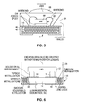
- Fig. 3 is a cross-sectional view of an LED package 30 where a central portion of the substrate 32 is formed of doped zinc oxide 34 having metal layers 36 forming partially overlapping electrodes.
- the doping may be cobalt.
- the varistor structure may be formed by depositing (e.g., evaporating or sputtering) or laminating thin metal films upon layers of the zinc oxide grains in a binder and then using heat and pressure to form a stacked laminated structure.
- the varistor becomes a monolithic block during the heating cycle, providing uniform energy dissipation in a small volume.
- the varistor portion of the substrate is surrounded by a conventional aluminum oxide, aluminum nitride, silicon carbide, or boron nitride ceramic substrate portion 40 for mechanical stability, hermetic sealing, and other properties.
- the ceramic substrate portion 40 may be formed by placing the varistor portion in a mold with aluminum oxide, aluminum nitride, silicon carbide, or boron nitride grains, then sintering the structure. Other techniques may be used.
- the varistor portion can be made any size and thickness and may be completely surrounded (including the top and bottom surfaces) by the aluminum oxide, aluminum nitride, silicon carbide, or boron nitride ceramic substrate portion or have any or all of its sides exposed if the varistor provides the desired properties for the substrate.
- a metallization step forms a metal via 42 extending from a top metal pad 14 to a bottom metal pad 22.
- the via 42 contacts the various varistor metal layers 36.
- the openings for the metal via may be formed during the molding process or may be drilled or etched.
- the various heating, pressure, metal deposition, and other processes for forming the varistor and the aluminum oxide, aluminum nitride, silicon carbide, or boron nitride ceramic substrate are compatible.
- the zinc oxide varistor may be first formed, followed by forming the ceramic substrate around the varistor, followed by a metallization step.
- the ceramic substrate may be first formed followed by forming the varistor.
- the varistor and ceramic substrate can be formed at the same time. The same heating steps can be performed on both structures.
- Solder or gold interconnects 18 are then provided over the metal pads 14. These interconnects may be solder balls, solder paste, stud-bumps, or a plated or otherwise deposited layer.
- the surface mounted LED chip 12 is then mounted so that its bottom electrodes align with the solder interconnects, and the structure is heated to melt the interconnects and form an electrical and structural bond between the LED chip 12, the varistor/substrate, and the backside metal pads 22.
- thermocompression bonding or thermosonic bonding would typically be used for bonding the LED chip 12 to the pads 14 through the use of gold interconnects.
- An LED chip having both contacts on the bottom side is sometimes referred to as a flip chip.
- the LED chip 12 is encapsulated using silicon or epoxy 23 with an optional phosphor powder incorporated into the encapsulation material if desirable for a particular light output.
- the heat-sinking of the LED chip 12 occurs through the combination of the metal, the varistor/substrate, and the PC board.
- Any voltage surge applied to a backside pad 22 will be shorted across pads 22 by the reduced resistance of the varistor so as to shunt the current away from the LED chip 12.
- Fig. 4 is cross-sectional view of another embodiment of the invention where the entire ceramic substrate is a varistor 50 formed of doped zinc oxide 52 and metal layers 54.
- the varistor 50 is at least partially surrounded by wrap-around metallization 56, which provides mechanical stability, heat conductivity, and enhanced electrical properties.
- wrap-around metallization 56 which provides mechanical stability, heat conductivity, and enhanced electrical properties.
- no through-metallization is required since the varistor metal layers 54 extend to the edge of the ceramic substrate.
- Fig. 5 is a cross-section of another embodiment of an LED package similar to that of Fig. 3 except that the LED chip 60 is not a flip chip but has its contacts on a top surface, which are connected via wires 62 to the pads 14 of the ceramic substrate.
- the LED chip 60 is attached to a metal pad of the ceramic substrate by solder or die attaches epoxy 63.
- a reflector 64 surrounds the LED chip 60 to reflect light through the top surface of the package.
- the reflective walls may be a refractive interface between two materials, a refractive index step from one encapsulant to another or to air, or a reflective metal slope.
- the reflective walls may also be formed by the ceramic material. For example, aluminum oxide is white and can thus act as a reflector and a diffuser.
- a molded lens 66 is formed over the LED chip 60.
- Fig. 6 is a cross-sectional view of another embodiment of the invention where the varistor 70 is formed along at least a portion of the outer surface of the aluminum oxide, aluminum nitride, silicon carbide, or boron nitride ceramic substrate 72.
- the varistor portion of the substrate may be formed along any portion of the aluminum oxide, aluminum nitride, silicon carbide, or boron nitride substrate.
- the metal layers 54 in the varistor alternately contact the two metal vias 42. Additional vias may be provided as desired.
- Fig. 7 is a top-down view of the structure of Fig. 6 showing that the varistor 70 portion completely surrounds the outer perimeter of the aluminum oxide, aluminum nitride, silicon carbide, or boron nitride substrate 72. Also shown are metal interconnects 18 for the anode and cathode terminals of the LED chip 12 coupled to metal pads 14. Four contacts are used for reproducible orientation of the chip 12 on the substrate.
- Fig. 8 is a cross-section of another embodiment of the invention where an aluminum nitride, aluminum oxide, silicon carbide, or boron nitride ceramic substrate 74 portion has formed on top of it a zinc oxide varistor 76 having a bottom metal layer 78 and an upper metal layer 80.
- Metal layers 78 and 80 are electrically coupled to contacts on the LED chip 12 and to the bottom metal pads 22.
- the varistor presents a low resistance path between metal layers 78 and 80 when a voltage surge is applied across metal pads 22.
- the varistor could also be formed on the bottom of the substrate.
- the embodiment of Fig. 8 is simple to form because the zinc oxide material is a single layer formed on top of the aluminum oxide, aluminum nitride, silicon carbide, or boron nitride substrate 74.
- the zinc oxide varistor may form any portion of the top or bottom surface of the ceramic substrate.
- the ceramic substrate 74 portion may be a conventional rectangular substrate. If desirable, additional metal layers may be interdigitated within the zinc oxide layer.
- Fig. 9 illustrates another embodiment of the invention, similar to Fig. 8, except that the metal layers 84 and 86 for the varistor 76 are formed on an upper surface of the zinc oxide layer so the varistor breaks down across the top surface between the ends of the two metal layers. A large breakdown voltage may be achieved with a thin zinc oxide layer.
- Another advantage of the structure of Fig. 9 is that the metal can be applied after the substrate has been completely manufactured such as by screen printing and firing.
- the varistor may also be formed on the bottom surface of the substrate.
- Fig. 10 illustrates another embodiment of the invention where the varistor 90 is formed on a top surface of the aluminum oxide, aluminum nitride, silicon carbide, or boron nitride ceramic substrate portion only near the edge of the substrate.
- the varistor may be formed along any number of sides of the substrate.
- the metal layer portions 92 are deposited on top of the ceramic substrate 74, and the varistor material is then formed over the metal layer portions 92.
- the varistor material on the left side of Fig. 10 is continuous with the varistor material on the right side of Fig. 10, and the varistor breaks down between the two metal layer portions 92.
- other electrode metal layer(s) for the varistor may be formed over the varistor material or may be formed as interdigitated metal layers in the varistor material so the varistor breaks down vertically instead of horizontally.
- the varistor portion of Fig. 10 may also be formed on a bottom surface of the substrate.
- the various packages described herein may be incorporated into another package.
- Such other package will typically include a lens, reflective walls, a base, and leads for connection to a PC board.
- the ceramic substrate incorporating the varistor may be directly attached to the PC board.
- the LED chip may be directly mounted on a submount, such as a semiconductor chip with conductive traces and active components, and the submount is then mounted to the ceramic substrate incorporating the varistor.
- the patterning of the metal layers contacting the zinc oxide may be used to select the desired breakdown voltage of the varistor for any of the embodiments described herein.
- the zinc oxide grains and other properties of the zinc oxide layer may also be adjusted to achieve a desired breakdown voltage.
- the ceramic substrate incorporating a metal oxide varistor has been shown for supporting and protecting an LED chip, the ceramic substrate may be used to protect any type of chip, such as a conventional integrated circuit chip.
- Various forms of the varistor may be incorporated using any pattern of electrodes and any shape of the varistor, using up any substrate volume. Multiple varistors can be connected in series and/or parallel.
- varistors may be formed of other metal oxides or a combination of such oxides with zinc oxide.
- examples of other oxides include Sb 2 O 3 , Bi 2 O 3 , CoO, MnO, and Cr 2 O 3 .
- Metal oxide varistors are described in more detail in the publication, "The Physics of Metal Oxide Varistors,” by Levinson and Philipp, Journal of Applied Physics, Volume 46, No. 3, March 1975, incorporated herein by reference.
Landscapes
- Engineering & Computer Science (AREA)
- Microelectronics & Electronic Packaging (AREA)
- Physics & Mathematics (AREA)
- Power Engineering (AREA)
- Condensed Matter Physics & Semiconductors (AREA)
- General Physics & Mathematics (AREA)
- Computer Hardware Design (AREA)
- Electromagnetism (AREA)
- Led Device Packages (AREA)
- Thermistors And Varistors (AREA)
Abstract
Description
- This invention relates to electrostatic discharge (ESD) protection of electronic devices and, more particularly, to ESD protection for a semiconductor chip (e.g., a light emitting diode) mounted on a ceramic substrate.
- Fig. 1 is a cross-sectional view of a prior art light emitting diode (LED)
package 10.Package 10 contains anLED chip 12 having cathode and anode contacts coupled, viametal interconnects 18, tometal pads 14 on aceramic substrate 16.Metal vias 20 extend throughsubstrate 16 and contactbackside metal pads 22. The LED chip is encapsulated byepoxy 23.Package 10 is typically solder-mounted onto a printed circuit board or incorporated into another package. Such other package typically includes a lens, reflective walls, a base, and leads. The various metal interconnects in combination with theceramic substrate 16 conduct heat from theLED chip 12 to the printed circuit board, which may include an additional heat sink. - LEDs are well known and are formed from semiconductor materials on a substrate. The
LED chip 12 substrate material may be a semiconductor, a conductor, or an insulator. - LEDs can be damaged by high voltages from ESD. It is common to provide ESD protection for an LED, such as providing a separate ESD protection circuit in the LED package or on the printed circuit board. Providing a separate ESD protection circuit in the LED package may increase the size of the package and/or reduce the light-emitting area of the
chip 12. Forming the ESD protection circuitry on the PC board or in the package also adds complexity in the manufacture of the PC board or package and thus adds cost to the circuit. - What is desirable is a technique for providing ESD protection without the need for forming ESD protection circuitry on the LED chip or as a separate element on the PC board or in the package.
- A metal oxide varistor comprising one or more zinc oxide layers is formed integral to a ceramic substrate. The portion of the ceramic substrate that is not the varistor may be typically formed of aluminum oxide, aluminum nitride, silicon carbide, or boron nitride. Metal oxide varistors are commonly used for transient voltage suppression. The fabrication techniques for metal oxide varistors are compatible with those used to form ceramic substrates.
- Accordingly, an ESD protection circuit is provided for an LED chip, or any other type of semiconductor chip, without the need for forming the ESD protection circuitry on the chip or providing a separate ESD protection circuit in the package or external to the package.
-
- Fig. 1 is a cross-sectional view of a prior art surface-mounted LED package.
- Fig. 2 is a cross-sectional view of a typical metal oxide varistor comprising zinc oxide grains.
- Fig. 3 is a cross-sectional view of an LED package incorporating a metal oxide varistor as an ESD protection circuit in the central portion of the ceramic substrate.
- Fig. 4 is a cross-sectional view of another embodiment of an LED package where the varistor forms almost the entire ceramic substrate.
- Fig. 5 is a cross-sectional view of an LED package where the LED chip electrodes are connected with wires to a ceramic substrate incorporating a metal oxide varistor.
- Fig. 6 is a cross-sectional view of another embodiment of an LED package where the ceramic substrate incorporates a metal oxide varistor around a periphery of the substrate.
- Fig. 7 is a top-down view of the structure of Fig. 6.
- Fig. 8 is a cross-sectional view of another embodiment of an LED package where the substrate incorporates a zinc oxide varistor as a top layer of the substrate and where the zinc oxide is sandwiched between two varistor electrodes.
- Fig. 9 is a cross-sectional view of another embodiment of an LED package where the substrate incorporates a zinc oxide varistor as a top layer of the substrate and where the varistor electrodes are formed on a top surface of the zinc oxide layer.
- Fig. 10 is a cross-sectional view of another embodiment of an LED package where the substrate incorporates a zinc oxide varistor as a top layer of the substrate along the outer portions of the substrate.
-
- Ceramic substrates are commonly used to provide a hermetic seal, electrical insulation, mechanical stability, and a conductive heat path for integrated circuits. Ceramic substrates are easy to form by mixing ceramic powder in a binder and casting it into the desired form. The ceramic grains may also be sintered under pressure to bind the grains together. Suitable metal patterns are then deposited on the formed ceramic substrate. Ceramic substrates typically comprise aluminum oxide, aluminum nitride, silicon carbide, or boron nitride particles.
- ESD protection circuitry generally operates to create a low resistance path between its terminals when a high voltage is applied across its terminals. There are many types of ESD protection circuits. One such ESD protection circuit is a metal oxide varistor. When a power surge or voltage spike is sensed, the varistor's resistance rapidly decreases, creating an instant shunt path, thereby preventing the current spike from being discharged through the protected components. A varistor acts similarly to back-to-back zener diodes.
- Fig. 2 is a cross-section of a simple metal oxide varistor comprising
zinc oxide grains 24 in abinder 26 sandwiched between twoelectrodes 28. The varistor is typically formed by mixing the zinc oxide grains with a binder and heating the grains under pressure to form a structure of conductive zinc oxide grains surrounded by electrically insulating barriers, creating varistor-like behavior. The number of grain-boundary interfaces between conducting electrodes determines the breakdown voltage of the device. High voltage applications require many grains between electrodes, while low voltage applications require few grains between the electrodes to establish the appropriate breakdown voltage. Varistors may be a single layer between electrodes or may be multiple layers, where each layer is sandwiched between opposing electrodes. The formation of zinc oxide varistors is well known. - The processing of these metal oxide varistors is compatible with the processing of standard ceramic substrates used for semiconductor chip packaging since the metal oxide is a ceramic. We use this compatibility to integrate the metal oxide varistor for ESD protection into the standard ceramic packaging. The range of integration ranges from the ceramic substrate having only a small portion forming the zinc oxide varistor to the substrate being completely formed by the zinc oxide varistor.
- The same or similar elements in the various figures are assigned the same numeral.
- Fig. 3 is a cross-sectional view of an
LED package 30 where a central portion of thesubstrate 32 is formed of dopedzinc oxide 34 havingmetal layers 36 forming partially overlapping electrodes. The doping may be cobalt. The varistor structure may be formed by depositing (e.g., evaporating or sputtering) or laminating thin metal films upon layers of the zinc oxide grains in a binder and then using heat and pressure to form a stacked laminated structure. The varistor becomes a monolithic block during the heating cycle, providing uniform energy dissipation in a small volume. - The varistor portion of the substrate is surrounded by a conventional aluminum oxide, aluminum nitride, silicon carbide, or boron nitride
ceramic substrate portion 40 for mechanical stability, hermetic sealing, and other properties. Theceramic substrate portion 40 may be formed by placing the varistor portion in a mold with aluminum oxide, aluminum nitride, silicon carbide, or boron nitride grains, then sintering the structure. Other techniques may be used. - The varistor portion can be made any size and thickness and may be completely surrounded (including the top and bottom surfaces) by the aluminum oxide, aluminum nitride, silicon carbide, or boron nitride ceramic substrate portion or have any or all of its sides exposed if the varistor provides the desired properties for the substrate.
- A metallization step forms a metal via 42 extending from a
top metal pad 14 to abottom metal pad 22. Thevia 42 contacts the variousvaristor metal layers 36. The openings for the metal via may be formed during the molding process or may be drilled or etched. - The various heating, pressure, metal deposition, and other processes for forming the varistor and the aluminum oxide, aluminum nitride, silicon carbide, or boron nitride ceramic substrate are compatible. The zinc oxide varistor may be first formed, followed by forming the ceramic substrate around the varistor, followed by a metallization step. Or, the ceramic substrate may be first formed followed by forming the varistor. Or, the varistor and ceramic substrate can be formed at the same time. The same heating steps can be performed on both structures.
- Solder or
gold interconnects 18 are then provided over themetal pads 14. These interconnects may be solder balls, solder paste, stud-bumps, or a plated or otherwise deposited layer. In one embodiment, the surface mountedLED chip 12 is then mounted so that its bottom electrodes align with the solder interconnects, and the structure is heated to melt the interconnects and form an electrical and structural bond between theLED chip 12, the varistor/substrate, and thebackside metal pads 22. In another embodiment, for bonding theLED chip 12 to thepads 14 through the use of gold interconnects, thermocompression bonding or thermosonic bonding would typically be used. An LED chip having both contacts on the bottom side is sometimes referred to as a flip chip. - The
LED chip 12 is encapsulated using silicon or epoxy 23 with an optional phosphor powder incorporated into the encapsulation material if desirable for a particular light output. - The heat-sinking of the
LED chip 12 occurs through the combination of the metal, the varistor/substrate, and the PC board. - Any voltage surge applied to a
backside pad 22 will be shorted acrosspads 22 by the reduced resistance of the varistor so as to shunt the current away from theLED chip 12. - Fig. 4 is cross-sectional view of another embodiment of the invention where the entire ceramic substrate is a
varistor 50 formed of dopedzinc oxide 52 and metal layers 54. Thevaristor 50 is at least partially surrounded by wrap-aroundmetallization 56, which provides mechanical stability, heat conductivity, and enhanced electrical properties. In the embodiment of Fig. 4, no through-metallization is required since thevaristor metal layers 54 extend to the edge of the ceramic substrate. - Fig. 5 is a cross-section of another embodiment of an LED package similar to that of Fig. 3 except that the
LED chip 60 is not a flip chip but has its contacts on a top surface, which are connected viawires 62 to thepads 14 of the ceramic substrate. TheLED chip 60 is attached to a metal pad of the ceramic substrate by solder or die attachesepoxy 63. - In the embodiment of Fig. 5, a
reflector 64 surrounds theLED chip 60 to reflect light through the top surface of the package. The reflective walls may be a refractive interface between two materials, a refractive index step from one encapsulant to another or to air, or a reflective metal slope. The reflective walls may also be formed by the ceramic material. For example, aluminum oxide is white and can thus act as a reflector and a diffuser. A moldedlens 66 is formed over theLED chip 60. - Fig. 6 is a cross-sectional view of another embodiment of the invention where the
varistor 70 is formed along at least a portion of the outer surface of the aluminum oxide, aluminum nitride, silicon carbide, or boronnitride ceramic substrate 72. The varistor portion of the substrate may be formed along any portion of the aluminum oxide, aluminum nitride, silicon carbide, or boron nitride substrate. The metal layers 54 in the varistor alternately contact the twometal vias 42. Additional vias may be provided as desired. - Fig. 7 is a top-down view of the structure of Fig. 6 showing that the
varistor 70 portion completely surrounds the outer perimeter of the aluminum oxide, aluminum nitride, silicon carbide, orboron nitride substrate 72. Also shown aremetal interconnects 18 for the anode and cathode terminals of theLED chip 12 coupled tometal pads 14. Four contacts are used for reproducible orientation of thechip 12 on the substrate. - Fig. 8 is a cross-section of another embodiment of the invention where an aluminum nitride, aluminum oxide, silicon carbide, or boron
nitride ceramic substrate 74 portion has formed on top of it azinc oxide varistor 76 having abottom metal layer 78 and anupper metal layer 80. Metal layers 78 and 80 are electrically coupled to contacts on theLED chip 12 and to thebottom metal pads 22. The varistor presents a low resistance path betweenmetal layers metal pads 22. The varistor could also be formed on the bottom of the substrate. - The embodiment of Fig. 8 is simple to form because the zinc oxide material is a single layer formed on top of the aluminum oxide, aluminum nitride, silicon carbide, or
boron nitride substrate 74. The zinc oxide varistor may form any portion of the top or bottom surface of the ceramic substrate. Theceramic substrate 74 portion may be a conventional rectangular substrate. If desirable, additional metal layers may be interdigitated within the zinc oxide layer. - Fig. 9 illustrates another embodiment of the invention, similar to Fig. 8, except that the metal layers 84 and 86 for the
varistor 76 are formed on an upper surface of the zinc oxide layer so the varistor breaks down across the top surface between the ends of the two metal layers. A large breakdown voltage may be achieved with a thin zinc oxide layer. Another advantage of the structure of Fig. 9 is that the metal can be applied after the substrate has been completely manufactured such as by screen printing and firing. The varistor may also be formed on the bottom surface of the substrate. - Fig. 10 illustrates another embodiment of the invention where the
varistor 90 is formed on a top surface of the aluminum oxide, aluminum nitride, silicon carbide, or boron nitride ceramic substrate portion only near the edge of the substrate. The varistor may be formed along any number of sides of the substrate. Themetal layer portions 92 are deposited on top of theceramic substrate 74, and the varistor material is then formed over themetal layer portions 92. In one embodiment, the varistor material on the left side of Fig. 10 is continuous with the varistor material on the right side of Fig. 10, and the varistor breaks down between the twometal layer portions 92. In another embodiment, other electrode metal layer(s) for the varistor may be formed over the varistor material or may be formed as interdigitated metal layers in the varistor material so the varistor breaks down vertically instead of horizontally. - The varistor portion of Fig. 10 may also be formed on a bottom surface of the substrate.
- The various packages described herein may be incorporated into another package. Such other package will typically include a lens, reflective walls, a base, and leads for connection to a PC board. Alternatively, the ceramic substrate incorporating the varistor may be directly attached to the PC board. Additionally, the LED chip may be directly mounted on a submount, such as a semiconductor chip with conductive traces and active components, and the submount is then mounted to the ceramic substrate incorporating the varistor.
- The patterning of the metal layers contacting the zinc oxide may be used to select the desired breakdown voltage of the varistor for any of the embodiments described herein. The zinc oxide grains and other properties of the zinc oxide layer may also be adjusted to achieve a desired breakdown voltage.
- Although the ceramic substrate incorporating a metal oxide varistor has been shown for supporting and protecting an LED chip, the ceramic substrate may be used to protect any type of chip, such as a conventional integrated circuit chip. Various forms of the varistor may be incorporated using any pattern of electrodes and any shape of the varistor, using up any substrate volume. Multiple varistors can be connected in series and/or parallel.
- Although a varistor comprising zinc oxide has been described, varistors may be formed of other metal oxides or a combination of such oxides with zinc oxide. Examples of other oxides include Sb2O3, Bi2O3, CoO, MnO, and Cr2O3. Metal oxide varistors are described in more detail in the publication, "The Physics of Metal Oxide Varistors," by Levinson and Philipp, Journal of Applied Physics, Volume 46, No. 3, March 1975, incorporated herein by reference. Those skilled in the art of manufacturing ceramic substrates will be able to form any of the embodiments described herein without undue experimentation since the methods of forming aluminum oxide, aluminum nitride, silicon carbide, and boron nitride substrates and metal oxide varistors are well known.
- Further information regarding metal oxide varistors is described in the article entitled "Improved Metal Oxide Varistor Packaging Technology for Transient Voltage Surge Suppressers (TVSS)," by Drabkin et al., incorporated herein by reference.
- Having described the invention in detail, those skilled in the art will appreciate that, given the present disclosure, modifications may be made to the invention without departing from the spirit of the inventive concepts described herein. Therefore, it is not intended that the scope of the invention be limited to the specific embodiments illustrated and described.
Claims (21)
- A device comprising:a ceramic substrate having a top surface and a bottom surface, the top surface having at least one metal electrode for electrical connection to an electrode of an overlying semiconductor device, the ceramic substrate comprising a metal oxide varistor that provides electrostatic discharge (ESD) protection of a semiconductor device mounted over a top surface of the ceramic substrate.
- The device of Claim 1 wherein the varistor comprises zinc oxide, and wherein the zinc oxide forms only a central portion of the ceramic substrate.
- The device of Claim 1 wherein the varistor comprises zinc oxide, and wherein the zinc oxide is located only around at least a portion of a periphery of the ceramic substrate.
- The device of Claim 1 wherein the varistor comprises zinc oxide, and wherein the zinc oxide is located on at least a portion of a top or bottom surface of the ceramic substrate that does not form the varistor.
- The device of Claim 1 wherein the varistor comprises zinc oxide, and wherein the zinc oxide comprises a majority of the material in the ceramic substrate.
- The device of Claim 1 wherein a portion of the ceramic substrate that is not a varistor comprises one of aluminum oxide, aluminum nitride, silicon carbide, or boron nitride, and the varistor comprises zinc oxide.
- The device of Claim 1 wherein the varistor comprises ceramic grains, and wherein the varistor comprises a plurality of metal layers sandwiching the ceramic grains, the metal layers being electrically connected to exposed substrate electrodes, the ceramic grains providing a low resistance path between the metal layers when an ESD voltage is applied across the metal layers.
- The device of Claim 1 wherein the varistor comprises ceramic grains, the varistor further comprising multiple overlying metal layers with the ceramic grains between the metal layers, the metal layers being electrically connected to metal electrodes on the substrate.
- The device of Claim 1 wherein the varistor comprises ceramic grains forming a surface, and wherein the varistor comprises a plurality of metal layers electrically connected to exposed substrate electrodes, the plurality of metal layers being in physical contact with only a single surface of the ceramic grains, the ceramic grains providing a low resistance path between the metal layers when an ESD voltage is applied across the metal layers.
- The device of Claim 1 further comprising a light emitting diode (LED) chip mounted on the top surface of the substrate and being protected from ESD by the varistor.
- The device of Claim 1 wherein the varistor forms part of a heat conduction path between the semiconductor device and a printed circuit board over which the substrate is mounted.
- The device of Claim 1 wherein the ceramic substrate has a top and bottom surface comprising one of aluminum oxide, aluminum nitride, silicon carbide, or boron nitride, and wherein the varistor comprises zinc oxide formed as one or more layers fixed to the top or bottom surface of the ceramic substrate, a first metal layer being formed to physically contact a top surface of the one or more layers, and a second metal layer being formed to physically contact a bottom surface of the one or more layers, the one or more layers providing a low resistance path between the first metal layer and the second metal layer when an ESD voltage is applied across the first metal layer and the second metal layer.
- The device of Claim 1 wherein the ceramic substrate has a top and bottom surface comprising one of aluminum oxide, aluminum nitride, silicon carbide, or boron nitride, and wherein the varistor comprises zinc oxide formed as a single layer fixed to the top or bottom surface of the ceramic substrate, a first metal layer being formed to physically contact a first surface of the single layer, and a second metal layer being formed to also physically contact the first surface of the single layer, the single layer providing a low resistance path between the first metal layer and the second metal layer when an ESD voltage is applied across the first metal layer and the second metal layer.
- The device of Claim 1 further comprising metal pads on a top surface of the ceramic substrate, for connection to the semiconductor device, and metal electrodes for electrical connection to a printed circuit board.
- The device of Claim 14 further comprising metal vias through the ceramic substrate for electrically connecting the metal pads to the metal electrodes.
- The device of Claim 14 wherein the metal pads are electrically connected to the metal electrodes by metal portions over a periphery of the ceramic substrate.
- The device of Claim 1 wherein the semiconductor device comprises a semiconductor chip directly affixed to the top surface of the ceramic substrate.
- A method for forming a ceramic substrate for providing electrostatic discharge (ESD) protection of a semiconductor device comprising:forming a ceramic substrate having a top surface and a bottom surface; andforming at least one metal electrode on the top surface of the ceramic substrate for electrical connection to an electrode of an overlying semiconductor device,the ceramic substrate comprising a metal oxide varistor that provides electrostatic discharge (ESD) protection to a semiconductor device mounted on the top surface of the ceramic substrate.
- The method of Claim 18 wherein the varistor comprises zinc oxide.
- The method of Claim 19 wherein a portion of the ceramic substrate does not form part of the varistor, the portion of the ceramic substrate that does not form part of the varistor comprising one of aluminum oxide, aluminum nitride, silicon carbide, or boron nitride.
- The method of Claim 18 wherein a portion of the ceramic substrate does not form part of the varistor, the portion of the ceramic substrate that does not form part of the varistor comprising one of aluminum oxide, aluminum nitride, silicon carbide, or boron nitride.
Applications Claiming Priority (2)
| Application Number | Priority Date | Filing Date | Title |
|---|---|---|---|
| US787657 | 1997-01-21 | ||
| US10/787,657 US7279724B2 (en) | 2004-02-25 | 2004-02-25 | Ceramic substrate for a light emitting diode where the substrate incorporates ESD protection |
Publications (3)
| Publication Number | Publication Date |
|---|---|
| EP1580809A2 true EP1580809A2 (en) | 2005-09-28 |
| EP1580809A3 EP1580809A3 (en) | 2008-07-09 |
| EP1580809B1 EP1580809B1 (en) | 2013-05-22 |
Family
ID=34861924
Family Applications (1)
| Application Number | Title | Priority Date | Filing Date |
|---|---|---|---|
| EP05100899.3A Active EP1580809B1 (en) | 2004-02-25 | 2005-02-09 | Ceramic substrate incorporating an ESD protection for a light emitting diode |
Country Status (4)
| Country | Link |
|---|---|
| US (2) | US7279724B2 (en) |
| EP (1) | EP1580809B1 (en) |
| JP (1) | JP5698424B2 (en) |
| TW (1) | TWI377692B (en) |
Cited By (31)
| Publication number | Priority date | Publication date | Assignee | Title |
|---|---|---|---|---|
| EP1958271A2 (en) * | 2005-11-22 | 2008-08-20 | Shocking Technologies, Inc. | A light-emitting device using voltage switchable dielectric material |
| DE102007044198A1 (en) * | 2007-09-17 | 2009-03-19 | Osram Opto Semiconductors Gmbh | Opto-electronic component e.g. service mountable device, has diode chip and electrostatic discharge protection element arranged on sides of carrier, where sides are opposite to each other |
| DE102007043681A1 (en) * | 2007-09-13 | 2009-03-26 | Osram Opto Semiconductors Gmbh | Optoelectronic component |
| CN101578710A (en) * | 2005-11-22 | 2009-11-11 | 肖克科技有限公司 | A light-emitting device using voltage switchable dielectric material |
| WO2009141266A1 (en) * | 2008-05-21 | 2009-11-26 | Epcos Ag | Electric component arrangement comprising a varistor and a semiconductor component |
| WO2009141439A1 (en) * | 2008-05-21 | 2009-11-26 | Epcos Ag | Electric component assembly comprising a varistor and a semiconductor component |
| DE102008024479A1 (en) * | 2008-05-21 | 2009-12-03 | Epcos Ag | Electrical component arrangement |
| DE102008057174A1 (en) * | 2008-11-13 | 2010-05-20 | Osram Opto Semiconductors Gmbh | Surface mountable device |
| DE102008054923A1 (en) * | 2008-12-18 | 2010-07-01 | Infineon Technologies Ag | Power semiconductor module, has circuit carrier provided with power semiconductor chip that is arranged in housing, and capacitor with body integrated into sidewall of housing, where circuit carrier is designed as ceramic plate |
| US7793236B2 (en) | 2007-06-13 | 2010-09-07 | Shocking Technologies, Inc. | System and method for including protective voltage switchable dielectric material in the design or simulation of substrate devices |
| US7932807B2 (en) | 2008-03-28 | 2011-04-26 | Tdk Corporation | Varistor |
| US7932806B2 (en) | 2007-03-30 | 2011-04-26 | Tdk Corporation | Varistor and light emitting device |
| CN101276664B (en) * | 2007-03-30 | 2011-06-22 | Tdk株式会社 | Varistor and light emitting device |
| US7968014B2 (en) | 2006-07-29 | 2011-06-28 | Shocking Technologies, Inc. | Device applications for voltage switchable dielectric material having high aspect ratio particles |
| US8117743B2 (en) | 1999-08-27 | 2012-02-21 | Shocking Technologies, Inc. | Methods for fabricating current-carrying structures using voltage switchable dielectric materials |
| US8163595B2 (en) | 2006-09-24 | 2012-04-24 | Shocking Technologies, Inc. | Formulations for voltage switchable dielectric materials having a stepped voltage response and methods for making the same |
| US8203421B2 (en) | 2008-04-14 | 2012-06-19 | Shocking Technologies, Inc. | Substrate device or package using embedded layer of voltage switchable dielectric material in a vertical switching configuration |
| US8206614B2 (en) | 2008-01-18 | 2012-06-26 | Shocking Technologies, Inc. | Voltage switchable dielectric material having bonded particle constituents |
| US8272123B2 (en) | 2009-01-27 | 2012-09-25 | Shocking Technologies, Inc. | Substrates having voltage switchable dielectric materials |
| US8310064B2 (en) | 2005-11-22 | 2012-11-13 | Shocking Technologies, Inc. | Semiconductor devices including voltage switchable materials for over-voltage protection |
| EP2544254A1 (en) * | 2010-03-01 | 2013-01-09 | Panasonic Corporation | Substrate for light emitting element, method for manufacturing same, and light emitting device |
| US8362871B2 (en) | 2008-11-05 | 2013-01-29 | Shocking Technologies, Inc. | Geometric and electric field considerations for including transient protective material in substrate devices |
| US8399773B2 (en) | 2009-01-27 | 2013-03-19 | Shocking Technologies, Inc. | Substrates having voltage switchable dielectric materials |
| WO2014000988A1 (en) * | 2012-06-27 | 2014-01-03 | Osram Opto Semiconductors Gmbh | Optoelectronic component and method for producing an optoelectronic component |
| US8968606B2 (en) | 2009-03-26 | 2015-03-03 | Littelfuse, Inc. | Components having voltage switchable dielectric materials |
| US9054016B2 (en) | 2008-11-28 | 2015-06-09 | Osram Opto Semiconductors Gmbh | Radiation-emitting semiconductor chip |
| US9053844B2 (en) | 2009-09-09 | 2015-06-09 | Littelfuse, Inc. | Geometric configuration or alignment of protective material in a gap structure for electrical devices |
| US9208930B2 (en) | 2008-09-30 | 2015-12-08 | Littelfuse, Inc. | Voltage switchable dielectric material containing conductive core shelled particles |
| US9208931B2 (en) | 2008-09-30 | 2015-12-08 | Littelfuse, Inc. | Voltage switchable dielectric material containing conductor-on-conductor core shelled particles |
| US9224728B2 (en) | 2010-02-26 | 2015-12-29 | Littelfuse, Inc. | Embedded protection against spurious electrical events |
| US9320135B2 (en) | 2010-02-26 | 2016-04-19 | Littelfuse, Inc. | Electric discharge protection for surface mounted and embedded components |
Families Citing this family (132)
| Publication number | Priority date | Publication date | Assignee | Title |
|---|---|---|---|---|
| US20100038119A1 (en) * | 1999-08-27 | 2010-02-18 | Lex Kosowsky | Metal Deposition |
| US20100040896A1 (en) * | 1999-08-27 | 2010-02-18 | Lex Kosowsky | Metal Deposition |
| US20100038121A1 (en) * | 1999-08-27 | 2010-02-18 | Lex Kosowsky | Metal Deposition |
| CN102290409B (en) | 2003-04-01 | 2014-01-15 | 夏普株式会社 | Light-emitting apparatus |
| US20080025030A9 (en) * | 2003-09-23 | 2008-01-31 | Lee Kong W | Ceramic packaging for high brightness LED devices |
| US7854535B2 (en) * | 2003-09-23 | 2010-12-21 | Avago Technologies Ecbu Ip (Singapore) Pte. Ltd. | Ceramic packaging for high brightness LED devices |
| KR20050034936A (en) * | 2003-10-10 | 2005-04-15 | 삼성전기주식회사 | Wavelength - converted light emitting diode package using phosphor and manufacturing method |
| JP2006086274A (en) * | 2004-09-15 | 2006-03-30 | Taiyo Yuden Co Ltd | Stacked varistor, mounting structure thereof, and varistor module |
| JP2006086469A (en) * | 2004-09-17 | 2006-03-30 | Matsushita Electric Ind Co Ltd | Semiconductor light-emitting device, illumination module, illuminator, and method of manufacturing the semiconductor light-emitting device |
| US8679674B2 (en) | 2005-03-25 | 2014-03-25 | Front Edge Technology, Inc. | Battery with protective packaging |
| US7846579B2 (en) | 2005-03-25 | 2010-12-07 | Victor Krasnov | Thin film battery with protective packaging |
| WO2006106717A1 (en) * | 2005-04-01 | 2006-10-12 | Matsushita Electric Industrial Co., Ltd. | Varistor and electronic component module using same |
| JP4915058B2 (en) * | 2005-06-06 | 2012-04-11 | パナソニック株式会社 | LED component and manufacturing method thereof |
| US20070200133A1 (en) * | 2005-04-01 | 2007-08-30 | Akira Hashimoto | Led assembly and manufacturing method |
| US7505239B2 (en) * | 2005-04-14 | 2009-03-17 | Tdk Corporation | Light emitting device |
| US7348212B2 (en) * | 2005-09-13 | 2008-03-25 | Philips Lumileds Lighting Company Llc | Interconnects for semiconductor light emitting devices |
| US7736945B2 (en) * | 2005-06-09 | 2010-06-15 | Philips Lumileds Lighting Company, Llc | LED assembly having maximum metal support for laser lift-off of growth substrate |
| US20060289887A1 (en) * | 2005-06-24 | 2006-12-28 | Jabil Circuit, Inc. | Surface mount light emitting diode (LED) assembly with improved power dissipation |
| WO2007002644A2 (en) * | 2005-06-27 | 2007-01-04 | Lamina Lighting, Inc. | Light emitting diode package and method for making same |
| KR100674857B1 (en) | 2005-07-04 | 2007-01-29 | 삼성전기주식회사 | Led pkg and its method having improved esd capability |
| US20070015300A1 (en) * | 2005-07-15 | 2007-01-18 | Yu-Chuan Liu | Method for fabricating a light-emitting device |
| KR100629521B1 (en) * | 2005-07-29 | 2006-09-28 | 삼성전자주식회사 | Led package structure and manufacturing method, and led array module |
| JP2007088173A (en) * | 2005-09-21 | 2007-04-05 | Tdk Corp | Laminated chip varistor and method for manufacturing electronic apparatus |
| US7671468B2 (en) * | 2005-09-30 | 2010-03-02 | Tdk Corporation | Light emitting apparatus |
| JP4146464B2 (en) * | 2005-10-11 | 2008-09-10 | Tdk株式会社 | Light emitting device |
| US20100263200A1 (en) * | 2005-11-22 | 2010-10-21 | Lex Kosowsky | Wireless communication device using voltage switchable dielectric material |
| US20070126020A1 (en) * | 2005-12-03 | 2007-06-07 | Cheng Lin | High-power LED chip packaging structure and fabrication method thereof |
| US8030575B2 (en) * | 2005-12-29 | 2011-10-04 | Sensor Electronic Technology, Inc. | Mounting structure providing electrical surge protection |
| WO2007081719A2 (en) | 2006-01-05 | 2007-07-19 | Illumitex, Inc. | Separate optical device for directing light from an led |
| TWI284433B (en) * | 2006-02-23 | 2007-07-21 | Novalite Optronics Corp | Light emitting diode package and fabricating method thereof |
| TWI303872B (en) * | 2006-03-13 | 2008-12-01 | Ind Tech Res Inst | High power light emitting device assembly with esd preotection ability and the method of manufacturing the same |
| JP4577250B2 (en) * | 2006-03-27 | 2010-11-10 | Tdk株式会社 | Varistor and light emitting device |
| US9780268B2 (en) * | 2006-04-04 | 2017-10-03 | Cree, Inc. | Submount based surface mount device (SMD) light emitter components and methods |
| USD738832S1 (en) | 2006-04-04 | 2015-09-15 | Cree, Inc. | Light emitting diode (LED) package |
| JP4867511B2 (en) * | 2006-07-19 | 2012-02-01 | Tdk株式会社 | Varistor and light emitting device |
| US20080029405A1 (en) * | 2006-07-29 | 2008-02-07 | Lex Kosowsky | Voltage switchable dielectric material having conductive or semi-conductive organic material |
| EP2067145A2 (en) * | 2006-09-24 | 2009-06-10 | Shocking Technologies, Inc. | Technique for plating substrate devices using voltage switchable dielectric material and light assistance |
| WO2008038924A1 (en) * | 2006-09-28 | 2008-04-03 | Seoul Opto Device Co., Ltd. | Ultraviolet light emitting diode package |
| KR100774218B1 (en) * | 2006-09-28 | 2007-11-08 | 엘지전자 주식회사 | Lens, a method for manufacturing it and light emitting device package |
| EP2070123A2 (en) | 2006-10-02 | 2009-06-17 | Illumitex, Inc. | Led system and method |
| KR100845856B1 (en) * | 2006-12-21 | 2008-07-14 | 엘지전자 주식회사 | LED package and method of manufacturing the same |
| US7902564B2 (en) * | 2006-12-22 | 2011-03-08 | Koninklijke Philips Electronics N.V. | Multi-grain luminescent ceramics for light emitting devices |
| KR100851183B1 (en) * | 2006-12-27 | 2008-08-08 | 엘지이노텍 주식회사 | Semiconductor light emitting device package |
| TWI342075B (en) * | 2007-01-08 | 2011-05-11 | Ledtech Electronics Corp | Ceramic package for led |
| US20080169480A1 (en) * | 2007-01-11 | 2008-07-17 | Visera Technologies Company Limited | Optoelectronic device package and packaging method thereof |
| US20080224815A1 (en) * | 2007-03-13 | 2008-09-18 | Tatsuya Inoue | Electrostatic discharge protection component, and electronic component module using the same |
| US20080225449A1 (en) * | 2007-03-13 | 2008-09-18 | Tatsuya Inoue | Electrostatic discharge protection component, and electronic component module using the same |
| WO2008129877A1 (en) * | 2007-04-17 | 2008-10-30 | Panasonic Corporation | Led-mounting board |
| EP1990834B1 (en) * | 2007-05-10 | 2012-08-15 | Texas Instruments France | Local integration of non-linear sheet in integrated circuit packages for ESD/EOS protection |
| JP4978302B2 (en) * | 2007-05-11 | 2012-07-18 | Tdk株式会社 | Varistor and light emitting device |
| TW200849395A (en) * | 2007-06-01 | 2008-12-16 | Univ Chang Gung | Thin-film ZnO varistor and manufacturing method and application thereof |
| US7911059B2 (en) * | 2007-06-08 | 2011-03-22 | SeniLEDS Optoelectronics Co., Ltd | High thermal conductivity substrate for a semiconductor device |
| JP5034723B2 (en) * | 2007-07-05 | 2012-09-26 | Tdk株式会社 | Surge absorbing element and light emitting device |
| US20090050856A1 (en) * | 2007-08-20 | 2009-02-26 | Lex Kosowsky | Voltage switchable dielectric material incorporating modified high aspect ratio particles |
| US20090143216A1 (en) * | 2007-12-03 | 2009-06-04 | General Electric Company | Composition and method |
| CN101465347A (en) * | 2007-12-17 | 2009-06-24 | 富士迈半导体精密工业(上海)有限公司 | Light source die set and method of manufacturing the same |
| EP2240968A1 (en) | 2008-02-08 | 2010-10-20 | Illumitex, Inc. | System and method for emitter layer shaping |
| US20090220771A1 (en) * | 2008-02-12 | 2009-09-03 | Robert Fleming | Voltage switchable dielectric material with superior physical properties for structural applications |
| US8310043B2 (en) * | 2008-03-25 | 2012-11-13 | Bridge Semiconductor Corporation | Semiconductor chip assembly with post/base heat spreader with ESD protection layer |
| US8329510B2 (en) * | 2008-03-25 | 2012-12-11 | Bridge Semiconductor Corporation | Method of making a semiconductor chip assembly with a post/base heat spreader with an ESD protection layer |
| KR101457207B1 (en) | 2008-06-30 | 2014-11-03 | 서울바이오시스 주식회사 | Light emitting diode having electrostatic discharge protect device |
| JP2008252150A (en) * | 2008-07-22 | 2008-10-16 | Tdk Corp | Laminated chip varistor |
| JP2008263236A (en) * | 2008-07-22 | 2008-10-30 | Tdk Corp | Electronic equipment |
| US8269408B2 (en) * | 2008-08-12 | 2012-09-18 | Helio Optoelectronics Corporation | LED base structure with embedded capacitor |
| US7871842B2 (en) * | 2008-10-03 | 2011-01-18 | E. I. Du Pont De Nemours And Company | Production process for surface-mounting ceramic LED package, surface-mounting ceramic LED package produced by said production process, and mold for producing said package |
| TW201034256A (en) | 2008-12-11 | 2010-09-16 | Illumitex Inc | Systems and methods for packaging light-emitting diode devices |
| US20100155021A1 (en) * | 2008-12-22 | 2010-06-24 | Chin Hsiang Chiang | Heat exchange cooling structure |
| US20100157492A1 (en) * | 2008-12-23 | 2010-06-24 | General Electric Company | Electronic device and associated method |
| US9226391B2 (en) | 2009-01-27 | 2015-12-29 | Littelfuse, Inc. | Substrates having voltage switchable dielectric materials |
| TWI413284B (en) * | 2009-02-24 | 2013-10-21 | Ind Tech Res Inst | Light-emitting diode package structure |
| US8692274B2 (en) | 2009-02-24 | 2014-04-08 | Industrial Technology Research Institute | Light emitting diode package structure |
| US8445917B2 (en) * | 2009-03-20 | 2013-05-21 | Cree, Inc. | Bidirectional silicon carbide transient voltage suppression devices |
| TWI467706B (en) * | 2009-04-09 | 2015-01-01 | Ind Tech Res Inst | Ceramic substrate and method for fabricating the same |
| US8629473B2 (en) * | 2009-08-13 | 2014-01-14 | Toyoda Gosei Co., Ltd. | Semiconductor light-emitting element, semiconductor light-emitting device, method for producing semiconductor light-emitting element, method for producing semiconductor light-emitting device, illumination device using semiconductor light-emitting device, and electronic apparatus |
| US8585253B2 (en) | 2009-08-20 | 2013-11-19 | Illumitex, Inc. | System and method for color mixing lens array |
| US8449128B2 (en) | 2009-08-20 | 2013-05-28 | Illumitex, Inc. | System and method for a lens and phosphor layer |
| WO2011037876A1 (en) * | 2009-09-25 | 2011-03-31 | Cree, Inc. | Lighting device having heat dissipation element |
| WO2011084252A2 (en) * | 2009-12-21 | 2011-07-14 | Saint-Gobain Ceramics & Plastics, Inc. | Electrostatic dissipative articles and method of making |
| US8286886B2 (en) * | 2009-12-23 | 2012-10-16 | Hynix Semiconductor Inc. | LED package and RFID system including the same |
| KR20110080318A (en) * | 2010-01-05 | 2011-07-13 | 엘지이노텍 주식회사 | Light emitting device package |
| US9082622B2 (en) | 2010-02-26 | 2015-07-14 | Littelfuse, Inc. | Circuit elements comprising ferroic materials |
| CN102201399B (en) * | 2010-03-22 | 2016-04-13 | 晶元光电股份有限公司 | Light-emitting component |
| JP5403370B2 (en) * | 2010-05-17 | 2014-01-29 | 株式会社村田製作所 | ESD protection device |
| US8476659B2 (en) * | 2010-07-15 | 2013-07-02 | Tsmc Solid State Lighting Ltd. | Light emitting device |
| US8304797B2 (en) * | 2010-07-29 | 2012-11-06 | Osram Sylvania Inc. | Light emitting diode light source having a ceramic substrate |
| US8534901B2 (en) | 2010-09-13 | 2013-09-17 | Teledyne Reynolds, Inc. | Collimating waveguide apparatus and method |
| WO2012035484A1 (en) | 2010-09-15 | 2012-03-22 | Koninklijke Philips Electronics N.V. | Embedded transient voltage suppression for light emitting devices |
| JP2014026993A (en) * | 2010-11-08 | 2014-02-06 | Panasonic Corp | Ceramic substrate and light emitting diode module |
| WO2012103928A1 (en) * | 2011-01-31 | 2012-08-09 | Osram Opto Semiconductors Gmbh | Arrangement of carriers for optoelectronic chips |
| CN103380502B (en) * | 2011-03-24 | 2016-10-12 | 株式会社村田制作所 | Light-emitting component pedestal substrate and LED component |
| US8608328B2 (en) | 2011-05-06 | 2013-12-17 | Teledyne Technologies Incorporated | Light source with secondary emitter conversion element |
| TWI474522B (en) * | 2011-05-12 | 2015-02-21 | 矽品精密工業股份有限公司 | Package structure and method of making same |
| KR101241133B1 (en) | 2011-06-29 | 2013-03-11 | (주) 아모엘이디 | Non-shrinkage varistor substrate, led package having the same and method for manufacturing non-shrinkage varistor substrate |
| JP6062429B2 (en) | 2011-07-15 | 2017-01-18 | コーニンクレッカ フィリップス エヌ ヴェKoninklijke Philips N.V. | Method for bonding a semiconductor device to a support substrate |
| WO2013027413A1 (en) * | 2011-08-25 | 2013-02-28 | パナソニック株式会社 | Protection element and light emitting device using same |
| US8865340B2 (en) | 2011-10-20 | 2014-10-21 | Front Edge Technology Inc. | Thin film battery packaging formed by localized heating |
| KR101915303B1 (en) * | 2011-10-24 | 2018-11-06 | 닛세이 에이. 에스. 비 기카이 가부시키가이샤 | Injection blow molding device, mold unit used therefor, and injection blow molding method |
| DE102012101606A1 (en) | 2011-10-28 | 2013-05-02 | Epcos Ag | ESD protection device and device with an ESD protection device and an LED |
| US9887429B2 (en) | 2011-12-21 | 2018-02-06 | Front Edge Technology Inc. | Laminated lithium battery |
| US8864954B2 (en) | 2011-12-23 | 2014-10-21 | Front Edge Technology Inc. | Sputtering lithium-containing material with multiple targets |
| US9077000B2 (en) | 2012-03-29 | 2015-07-07 | Front Edge Technology, Inc. | Thin film battery and localized heat treatment |
| US9257695B2 (en) | 2012-03-29 | 2016-02-09 | Front Edge Technology, Inc. | Localized heat treatment of battery component films |
| US9735198B2 (en) * | 2012-03-30 | 2017-08-15 | Cree, Inc. | Substrate based light emitter devices, components, and related methods |
| US10134961B2 (en) | 2012-03-30 | 2018-11-20 | Cree, Inc. | Submount based surface mount device (SMD) light emitter components and methods |
| US10222032B2 (en) | 2012-03-30 | 2019-03-05 | Cree, Inc. | Light emitter components and methods having improved electrical contacts |
| DE102012104494A1 (en) * | 2012-05-24 | 2013-11-28 | Epcos Ag | light emitting diode device |
| JP5832956B2 (en) | 2012-05-25 | 2015-12-16 | 株式会社東芝 | Semiconductor light emitting device |
| WO2014035143A1 (en) * | 2012-08-28 | 2014-03-06 | ㈜ 아모엘이디 | Non-shrink varistor substrate and production method for same |
| KR101483259B1 (en) * | 2012-08-28 | 2015-01-14 | 주식회사 아모센스 | Non-shrinkage varistor substrate and method for manufacturing the same |
| US9159964B2 (en) | 2012-09-25 | 2015-10-13 | Front Edge Technology, Inc. | Solid state battery having mismatched battery cells |
| US8753724B2 (en) | 2012-09-26 | 2014-06-17 | Front Edge Technology Inc. | Plasma deposition on a partially formed battery through a mesh screen |
| US9356320B2 (en) | 2012-10-15 | 2016-05-31 | Front Edge Technology Inc. | Lithium battery having low leakage anode |
| WO2014092296A1 (en) * | 2012-12-14 | 2014-06-19 | ㈜ 아모엘이디 | Varistor substrate in which thermal via is formed, and method for manufacturing same |
| CN103456871B (en) * | 2013-09-23 | 2016-05-25 | 电子科技大学 | Improve the fluorescent coating structure of pc-LEDs spatial light uniformity of chromaticity |
| JP6355492B2 (en) | 2013-10-03 | 2018-07-11 | アルパッド株式会社 | Composite resin and electronic device |
| DE102013112881A1 (en) * | 2013-11-21 | 2015-05-21 | Osram Opto Semiconductors Gmbh | Optoelectronic semiconductor chip |
| JP6539035B2 (en) | 2014-01-08 | 2019-07-03 | ローム株式会社 | Chip parts |
| CN103824846A (en) * | 2014-03-13 | 2014-05-28 | 杭州明果教育咨询有限公司 | Multi-field-effect transistor integrated module |
| DE102014115375A1 (en) * | 2014-08-08 | 2016-02-11 | Epcos Ag | Carrier for an LED |
| KR102261953B1 (en) * | 2015-01-14 | 2021-06-08 | 엘지이노텍 주식회사 | Light emitting device, light emitting device package having the same, and light system having the same |
| US10008739B2 (en) | 2015-02-23 | 2018-06-26 | Front Edge Technology, Inc. | Solid-state lithium battery with electrolyte |
| KR102292640B1 (en) | 2015-03-06 | 2021-08-23 | 삼성전자주식회사 | Light Emitting Device Package and electronic device including light emitting device |
| JP6468057B2 (en) * | 2015-04-28 | 2019-02-13 | 日亜化学工業株式会社 | Light emitting element |
| KR102601579B1 (en) | 2015-12-16 | 2023-11-13 | 삼성전자주식회사 | Substrate and light emitting device package using the same |
| DE102016100352A1 (en) * | 2016-01-11 | 2017-07-13 | Epcos Ag | Component carrier with ESD protection function and method of manufacture |
| DE102016107497B4 (en) | 2016-03-24 | 2020-01-30 | Tdk Electronics Ag | Multi-LED system and method for its production |
| DE102016107495B4 (en) * | 2016-04-22 | 2022-04-14 | Tdk Electronics Ag | Multi-layer carrier system, method for producing a multi-layer carrier system and use of a multi-layer carrier system |
| US10672957B2 (en) | 2017-07-19 | 2020-06-02 | Cree, Inc. | LED apparatuses and methods for high lumen output density |
| WO2019051780A1 (en) * | 2017-09-15 | 2019-03-21 | 厦门市三安光电科技有限公司 | White light led package structure and white light source system |
| TWI705585B (en) * | 2017-09-25 | 2020-09-21 | 致伸科技股份有限公司 | Light source module |
| EP3582592A1 (en) * | 2018-06-13 | 2019-12-18 | Valeo Iluminacion | Printed citcuit board, card edge connector socket, electronic assembly and automotive lighting device |
| CN110137141A (en) * | 2019-04-30 | 2019-08-16 | 华南理工大学 | A kind of metallization removal ceramic substrate and its welding method with capillary slot structure |
Citations (3)
| Publication number | Priority date | Publication date | Assignee | Title |
|---|---|---|---|---|
| US3743897A (en) | 1971-08-05 | 1973-07-03 | Gen Electric | Hybrid circuit arrangement with metal oxide varistor shunt |
| US4506285A (en) | 1982-08-20 | 1985-03-19 | Siemens Aktiengesellschaft | Substrate made of varistor material having a plurality of electronic components mounted thereon |
| US5889308A (en) | 1996-08-09 | 1999-03-30 | Hyundai Electronics Industries Co., Ltd. | Semiconductor device having an electrostatic discharging protection circuit using a non-ohmic material |
Family Cites Families (25)
| Publication number | Priority date | Publication date | Assignee | Title |
|---|---|---|---|---|
| US3679950A (en) * | 1971-04-16 | 1972-07-25 | Nl Industries Inc | Ceramic capacitors |
| GB1346851A (en) * | 1971-05-21 | 1974-02-13 | Matsushita Electric Ind Co Ltd | Varistors |
| US3965552A (en) * | 1972-07-24 | 1976-06-29 | N L Industries, Inc. | Process for forming internal conductors and electrodes |
| US5290375A (en) * | 1989-08-05 | 1994-03-01 | Nippondenso Co., Ltd. | Process for manufacturing ceramic multilayer substrate |
| US5176772A (en) * | 1989-10-05 | 1993-01-05 | Asahi Glass Company Ltd. | Process for fabricating a multilayer ceramic circuit board |
| GB9005990D0 (en) * | 1990-03-16 | 1990-05-09 | Ecco Ltd | Varistor powder compositions |
| WO1993004998A1 (en) * | 1991-09-12 | 1993-03-18 | The Dow Chemical Company | Method of making co-fired, multilayer substrates |
| JPH05275269A (en) * | 1992-03-30 | 1993-10-22 | Toshiba Corp | Multilayer ceramic electronic component |
| JPH05335174A (en) * | 1992-05-28 | 1993-12-17 | Murata Mfg Co Ltd | Laminated ceramic electronic component |
| JP3336198B2 (en) * | 1996-06-18 | 2002-10-21 | マルコン電子株式会社 | Multilayer ceramic varistor |
| JP3481778B2 (en) * | 1996-06-28 | 2003-12-22 | 京セラ株式会社 | Aluminum nitride sintered body and method for producing the same |
| JPH10308582A (en) * | 1997-05-07 | 1998-11-17 | Denso Corp | Multilayered wiring board |
| JPH114535A (en) * | 1997-06-12 | 1999-01-06 | Murata Mfg Co Ltd | Protection circuit and compound protection device |
| JPH11186053A (en) * | 1997-12-18 | 1999-07-09 | Matsushita Electric Ind Co Ltd | Composite component and its manufacture |
| JPH11251644A (en) * | 1998-02-27 | 1999-09-17 | Matsushita Electron Corp | Semiconductor light emitting device |
| JP3449599B2 (en) * | 1999-03-26 | 2003-09-22 | Tdk株式会社 | Multilayer chip varistor |
| JP2001015815A (en) * | 1999-04-28 | 2001-01-19 | Sanken Electric Co Ltd | Semiconductor light-emitting device |
| US6535105B2 (en) * | 2000-03-30 | 2003-03-18 | Avx Corporation | Electronic device and process of making electronic device |
| JP2001307947A (en) * | 2000-04-25 | 2001-11-02 | Tdk Corp | Laminated chip component and its manufacturing method |
| TW492202B (en) * | 2001-06-05 | 2002-06-21 | South Epitaxy Corp | Structure of III-V light emitting diode (LED) arranged in flip chip configuration having structure for preventing electrostatic discharge |
| US20030043012A1 (en) * | 2001-08-30 | 2003-03-06 | Kaori Shiraishi | Zinc oxide varistor and method of manufacturing same |
| JP2004014963A (en) * | 2002-06-11 | 2004-01-15 | Matsushita Electric Ind Co Ltd | Component protected from static electricity |
| JP2004022976A (en) * | 2002-06-19 | 2004-01-22 | Murata Mfg Co Ltd | Stacked voltage nonlinear resistor and method of manufacturing the same |
| JP2003297634A (en) * | 2003-02-17 | 2003-10-17 | Tdk Corp | Electronic component |
| US7095053B2 (en) * | 2003-05-05 | 2006-08-22 | Lamina Ceramics, Inc. | Light emitting diodes packaged for high temperature operation |
-
2004
- 2004-02-25 US US10/787,657 patent/US7279724B2/en active Active
-
2005
- 2005-02-09 EP EP05100899.3A patent/EP1580809B1/en active Active
- 2005-02-18 JP JP2005042144A patent/JP5698424B2/en active Active
- 2005-02-22 TW TW094105247A patent/TWI377692B/en active
-
2007
- 2007-08-30 US US11/848,055 patent/US7768754B2/en active Active
Patent Citations (3)
| Publication number | Priority date | Publication date | Assignee | Title |
|---|---|---|---|---|
| US3743897A (en) | 1971-08-05 | 1973-07-03 | Gen Electric | Hybrid circuit arrangement with metal oxide varistor shunt |
| US4506285A (en) | 1982-08-20 | 1985-03-19 | Siemens Aktiengesellschaft | Substrate made of varistor material having a plurality of electronic components mounted thereon |
| US5889308A (en) | 1996-08-09 | 1999-03-30 | Hyundai Electronics Industries Co., Ltd. | Semiconductor device having an electrostatic discharging protection circuit using a non-ohmic material |
Cited By (49)
| Publication number | Priority date | Publication date | Assignee | Title |
|---|---|---|---|---|
| US8117743B2 (en) | 1999-08-27 | 2012-02-21 | Shocking Technologies, Inc. | Methods for fabricating current-carrying structures using voltage switchable dielectric materials |
| EP2490508A3 (en) * | 2005-11-22 | 2013-05-15 | Shocking Technologies, Inc. | A light-emitting device using voltage switchable dielectric material |
| EP1958271A2 (en) * | 2005-11-22 | 2008-08-20 | Shocking Technologies, Inc. | A light-emitting device using voltage switchable dielectric material |
| CN101578710A (en) * | 2005-11-22 | 2009-11-11 | 肖克科技有限公司 | A light-emitting device using voltage switchable dielectric material |
| US7825491B2 (en) | 2005-11-22 | 2010-11-02 | Shocking Technologies, Inc. | Light-emitting device using voltage switchable dielectric material |
| CN101578710B (en) * | 2005-11-22 | 2013-05-22 | 肖克科技有限公司 | A light-emitting device using voltage switchable dielectric material |
| EP1958271A4 (en) * | 2005-11-22 | 2009-12-23 | Shocking Technologies Inc | A light-emitting device using voltage switchable dielectric material |
| US8310064B2 (en) | 2005-11-22 | 2012-11-13 | Shocking Technologies, Inc. | Semiconductor devices including voltage switchable materials for over-voltage protection |
| US7968014B2 (en) | 2006-07-29 | 2011-06-28 | Shocking Technologies, Inc. | Device applications for voltage switchable dielectric material having high aspect ratio particles |
| US7968010B2 (en) | 2006-07-29 | 2011-06-28 | Shocking Technologies, Inc. | Method for electroplating a substrate |
| US7968015B2 (en) * | 2006-07-29 | 2011-06-28 | Shocking Technologies, Inc. | Light-emitting diode device for voltage switchable dielectric material having high aspect ratio particles |
| US7981325B2 (en) | 2006-07-29 | 2011-07-19 | Shocking Technologies, Inc. | Electronic device for voltage switchable dielectric material having high aspect ratio particles |
| US8163595B2 (en) | 2006-09-24 | 2012-04-24 | Shocking Technologies, Inc. | Formulations for voltage switchable dielectric materials having a stepped voltage response and methods for making the same |
| US7932806B2 (en) | 2007-03-30 | 2011-04-26 | Tdk Corporation | Varistor and light emitting device |
| CN101276664B (en) * | 2007-03-30 | 2011-06-22 | Tdk株式会社 | Varistor and light emitting device |
| US7793236B2 (en) | 2007-06-13 | 2010-09-07 | Shocking Technologies, Inc. | System and method for including protective voltage switchable dielectric material in the design or simulation of substrate devices |
| DE102007043681B4 (en) | 2007-09-13 | 2022-01-20 | OSRAM Opto Semiconductors Gesellschaft mit beschränkter Haftung | optoelectronic component |
| DE102007043681A1 (en) * | 2007-09-13 | 2009-03-26 | Osram Opto Semiconductors Gmbh | Optoelectronic component |
| DE102007044198A1 (en) * | 2007-09-17 | 2009-03-19 | Osram Opto Semiconductors Gmbh | Opto-electronic component e.g. service mountable device, has diode chip and electrostatic discharge protection element arranged on sides of carrier, where sides are opposite to each other |
| US8206614B2 (en) | 2008-01-18 | 2012-06-26 | Shocking Technologies, Inc. | Voltage switchable dielectric material having bonded particle constituents |
| US7932807B2 (en) | 2008-03-28 | 2011-04-26 | Tdk Corporation | Varistor |
| US8203421B2 (en) | 2008-04-14 | 2012-06-19 | Shocking Technologies, Inc. | Substrate device or package using embedded layer of voltage switchable dielectric material in a vertical switching configuration |
| DE102008024480A1 (en) * | 2008-05-21 | 2009-12-03 | Epcos Ag | Electrical component arrangement |
| DE102008024481B4 (en) * | 2008-05-21 | 2021-04-15 | Tdk Electronics Ag | Electrical component assembly |
| DE102008024481A1 (en) * | 2008-05-21 | 2009-12-03 | Epcos Ag | Electrical component arrangement |
| WO2009141266A1 (en) * | 2008-05-21 | 2009-11-26 | Epcos Ag | Electric component arrangement comprising a varistor and a semiconductor component |
| US8378455B2 (en) | 2008-05-21 | 2013-02-19 | Epcos Ag | Electronic component arrangement comprising a varistor and a semiconductor component |
| US9196402B2 (en) | 2008-05-21 | 2015-11-24 | Epcos Ag | Electronic component assembly comprising a varistor and a semiconductor component |
| DE102008024479A1 (en) * | 2008-05-21 | 2009-12-03 | Epcos Ag | Electrical component arrangement |
| WO2009141439A1 (en) * | 2008-05-21 | 2009-11-26 | Epcos Ag | Electric component assembly comprising a varistor and a semiconductor component |
| US9177703B2 (en) | 2008-05-21 | 2015-11-03 | Epcos Ag | Electric component assembly |
| US9208931B2 (en) | 2008-09-30 | 2015-12-08 | Littelfuse, Inc. | Voltage switchable dielectric material containing conductor-on-conductor core shelled particles |
| US9208930B2 (en) | 2008-09-30 | 2015-12-08 | Littelfuse, Inc. | Voltage switchable dielectric material containing conductive core shelled particles |
| US8362871B2 (en) | 2008-11-05 | 2013-01-29 | Shocking Technologies, Inc. | Geometric and electric field considerations for including transient protective material in substrate devices |
| US8642902B2 (en) | 2008-11-13 | 2014-02-04 | Osram Opto Semiconductors Gmbh | Surface mountable device |
| DE102008057174A1 (en) * | 2008-11-13 | 2010-05-20 | Osram Opto Semiconductors Gmbh | Surface mountable device |
| US9590008B2 (en) | 2008-11-28 | 2017-03-07 | Osram Opto Semiconductors Gmbh | Radiation-emitting semiconductor chip |
| US9054016B2 (en) | 2008-11-28 | 2015-06-09 | Osram Opto Semiconductors Gmbh | Radiation-emitting semiconductor chip |
| DE102008054923A1 (en) * | 2008-12-18 | 2010-07-01 | Infineon Technologies Ag | Power semiconductor module, has circuit carrier provided with power semiconductor chip that is arranged in housing, and capacitor with body integrated into sidewall of housing, where circuit carrier is designed as ceramic plate |
| DE102008054923B4 (en) | 2008-12-18 | 2018-04-26 | Infineon Technologies Ag | Power semiconductor module with a high capacity capacitor integrated in the housing wall |
| US8399773B2 (en) | 2009-01-27 | 2013-03-19 | Shocking Technologies, Inc. | Substrates having voltage switchable dielectric materials |
| US8272123B2 (en) | 2009-01-27 | 2012-09-25 | Shocking Technologies, Inc. | Substrates having voltage switchable dielectric materials |
| US8968606B2 (en) | 2009-03-26 | 2015-03-03 | Littelfuse, Inc. | Components having voltage switchable dielectric materials |
| US9053844B2 (en) | 2009-09-09 | 2015-06-09 | Littelfuse, Inc. | Geometric configuration or alignment of protective material in a gap structure for electrical devices |
| US9320135B2 (en) | 2010-02-26 | 2016-04-19 | Littelfuse, Inc. | Electric discharge protection for surface mounted and embedded components |
| US9224728B2 (en) | 2010-02-26 | 2015-12-29 | Littelfuse, Inc. | Embedded protection against spurious electrical events |
| EP2544254A4 (en) * | 2010-03-01 | 2015-01-21 | Panasonic Corp | Substrate for light emitting element, method for manufacturing same, and light emitting device |
| EP2544254A1 (en) * | 2010-03-01 | 2013-01-09 | Panasonic Corporation | Substrate for light emitting element, method for manufacturing same, and light emitting device |
| WO2014000988A1 (en) * | 2012-06-27 | 2014-01-03 | Osram Opto Semiconductors Gmbh | Optoelectronic component and method for producing an optoelectronic component |
Also Published As
| Publication number | Publication date |
|---|---|
| US7279724B2 (en) | 2007-10-09 |
| US20050184387A1 (en) | 2005-08-25 |
| US7768754B2 (en) | 2010-08-03 |
| TWI377692B (en) | 2012-11-21 |
| TW200541108A (en) | 2005-12-16 |
| US20070297108A1 (en) | 2007-12-27 |
| EP1580809A3 (en) | 2008-07-09 |
| EP1580809B1 (en) | 2013-05-22 |
| JP5698424B2 (en) | 2015-04-08 |
| JP2005244220A (en) | 2005-09-08 |
Similar Documents
| Publication | Publication Date | Title |
|---|---|---|
| US7279724B2 (en) | Ceramic substrate for a light emitting diode where the substrate incorporates ESD protection | |
| EP2544254B1 (en) | Substrate for light emitting element, method for manufacturing same, and light emitting device | |
| EP3255686B1 (en) | Led package structure | |
| KR101360732B1 (en) | Led package | |
| US20060170113A1 (en) | Semiconductor device | |
| KR100658536B1 (en) | Array type semiconductor package | |
| JPWO2013121787A1 (en) | Light emitting device and manufacturing method thereof | |
| CN103890866B (en) | ESD protective component and component comprising ESD protective component and LED | |
| WO2008041813A1 (en) | Ceramic package and method of manufacturing the same | |
| KR100788931B1 (en) | Electron components package | |
| US7355251B2 (en) | Light emitting device | |
| CN201904368U (en) | LED (light emitting diode) surface-mounting package structure based on silicon substrate integrated with functional circuit | |
| JP2008270327A (en) | Electrostatic discharge protecting component and light-emitting diode module using the same | |
| US20080224816A1 (en) | Electrostatic discharge protection component, and electronic component module using the same | |
| TWI405319B (en) | Stacked integrated circuit chip assembly | |
| US20080225449A1 (en) | Electrostatic discharge protection component, and electronic component module using the same | |
| CN101546737A (en) | Package structure of compound semiconductor component and manufacturing method thereof | |
| JP2008270325A (en) | Electrostatic discharge protective component and light-emitting diode module using the same | |
| CN101501842B (en) | Semiconductor package and manufacturing method thereof | |
| KR100674857B1 (en) | Led pkg and its method having improved esd capability | |
| JP2008227137A (en) | Electrostatic countermeasure component and light-emitting diode module using the same | |
| KR100787951B1 (en) | SMD type ceramic package for LED | |
| KR100644315B1 (en) | Semiconductor device package | |
| KR101208635B1 (en) | Semiconductor substrate for led package and method for manufacturing thereof | |
| US8379356B2 (en) | Overvoltage protection device and its fabrication |
Legal Events
| Date | Code | Title | Description |
|---|---|---|---|
| PUAI | Public reference made under article 153(3) epc to a published international application that has entered the european phase |
Free format text: ORIGINAL CODE: 0009012 |
|
| AK | Designated contracting states |
Kind code of ref document: A2 Designated state(s): AT BE BG CH CY CZ DE DK EE ES FI FR GB GR HU IE IS IT LI LT LU MC NL PL PT RO SE SI SK TR |
|
| AX | Request for extension of the european patent |
Extension state: AL BA HR LV MK YU |
|
| RAP1 | Party data changed (applicant data changed or rights of an application transferred) |
Owner name: PHILIPS LUMILEDS LIGHTING COMPANY LLC |
|
| PUAL | Search report despatched |
Free format text: ORIGINAL CODE: 0009013 |
|
| AK | Designated contracting states |
Kind code of ref document: A3 Designated state(s): AT BE BG CH CY CZ DE DK EE ES FI FR GB GR HU IE IS IT LI LT LU MC NL PL PT RO SE SI SK TR |
|
| AX | Request for extension of the european patent |
Extension state: AL BA HR LV MK YU |
|
| 17P | Request for examination filed |
Effective date: 20090109 |
|
| AKX | Designation fees paid |
Designated state(s): DE |
|
| RBV | Designated contracting states (corrected) |
Designated state(s): AT BE BG CH CY CZ DE DK EE ES FI FR GB GR HU IE IS IT LI LT LU MC NL PL PT RO SE SI SK TR |
|
| 17Q | First examination report despatched |
Effective date: 20110415 |
|
| GRAP | Despatch of communication of intention to grant a patent |
Free format text: ORIGINAL CODE: EPIDOSNIGR1 |
|
| RIN1 | Information on inventor provided before grant (corrected) |
Inventor name: BHAT, JEROME, C. LUMILEDS LIGHTING US., LLC Inventor name: COLLINS, WILLIAM, D. LUMILEDS LIGHTING US., LLC |
|
| GRAS | Grant fee paid |
Free format text: ORIGINAL CODE: EPIDOSNIGR3 |
|
| GRAA | (expected) grant |
Free format text: ORIGINAL CODE: 0009210 |
|
| AK | Designated contracting states |
Kind code of ref document: B1 Designated state(s): AT BE BG CH CY CZ DE DK EE ES FI FR GB GR HU IE IS IT LI LT LU MC NL PL PT RO SE SI SK TR |
|
| REG | Reference to a national code |
Ref country code: GB Ref legal event code: FG4D |
|
| REG | Reference to a national code |
Ref country code: DE Ref legal event code: R081 Ref document number: 602005039661 Country of ref document: DE Owner name: LUMILEDS HOLDING B.V., NL Free format text: FORMER OWNER: LUMILEDS LIGHTING U.S., LLC, SAN JOSE, CALIF., US |
|
| REG | Reference to a national code |
Ref country code: CH Ref legal event code: EP |
|
| REG | Reference to a national code |
Ref country code: AT Ref legal event code: REF Ref document number: 613623 Country of ref document: AT Kind code of ref document: T Effective date: 20130615 |
|
| REG | Reference to a national code |
Ref country code: IE Ref legal event code: FG4D |
|
| REG | Reference to a national code |
Ref country code: DE Ref legal event code: R096 Ref document number: 602005039661 Country of ref document: DE Effective date: 20130718 |
|
| REG | Reference to a national code |
Ref country code: AT Ref legal event code: MK05 Ref document number: 613623 Country of ref document: AT Kind code of ref document: T Effective date: 20130522 |
|
| REG | Reference to a national code |
Ref country code: LT Ref legal event code: MG4D |
|
| PG25 | Lapsed in a contracting state [announced via postgrant information from national office to epo] |
Ref country code: GR Free format text: LAPSE BECAUSE OF FAILURE TO SUBMIT A TRANSLATION OF THE DESCRIPTION OR TO PAY THE FEE WITHIN THE PRESCRIBED TIME-LIMIT Effective date: 20130823 Ref country code: SE Free format text: LAPSE BECAUSE OF FAILURE TO SUBMIT A TRANSLATION OF THE DESCRIPTION OR TO PAY THE FEE WITHIN THE PRESCRIBED TIME-LIMIT Effective date: 20130522 Ref country code: PT Free format text: LAPSE BECAUSE OF FAILURE TO SUBMIT A TRANSLATION OF THE DESCRIPTION OR TO PAY THE FEE WITHIN THE PRESCRIBED TIME-LIMIT Effective date: 20130923 Ref country code: IS Free format text: LAPSE BECAUSE OF FAILURE TO SUBMIT A TRANSLATION OF THE DESCRIPTION OR TO PAY THE FEE WITHIN THE PRESCRIBED TIME-LIMIT Effective date: 20130922 Ref country code: ES Free format text: LAPSE BECAUSE OF FAILURE TO SUBMIT A TRANSLATION OF THE DESCRIPTION OR TO PAY THE FEE WITHIN THE PRESCRIBED TIME-LIMIT Effective date: 20130902 Ref country code: AT Free format text: LAPSE BECAUSE OF FAILURE TO SUBMIT A TRANSLATION OF THE DESCRIPTION OR TO PAY THE FEE WITHIN THE PRESCRIBED TIME-LIMIT Effective date: 20130522 Ref country code: LT Free format text: LAPSE BECAUSE OF FAILURE TO SUBMIT A TRANSLATION OF THE DESCRIPTION OR TO PAY THE FEE WITHIN THE PRESCRIBED TIME-LIMIT Effective date: 20130522 Ref country code: FI Free format text: LAPSE BECAUSE OF FAILURE TO SUBMIT A TRANSLATION OF THE DESCRIPTION OR TO PAY THE FEE WITHIN THE PRESCRIBED TIME-LIMIT Effective date: 20130522 Ref country code: SI Free format text: LAPSE BECAUSE OF FAILURE TO SUBMIT A TRANSLATION OF THE DESCRIPTION OR TO PAY THE FEE WITHIN THE PRESCRIBED TIME-LIMIT Effective date: 20130522 |
|
| REG | Reference to a national code |
Ref country code: NL Ref legal event code: VDEP Effective date: 20130522 |
|
| PG25 | Lapsed in a contracting state [announced via postgrant information from national office to epo] |
Ref country code: PL Free format text: LAPSE BECAUSE OF FAILURE TO SUBMIT A TRANSLATION OF THE DESCRIPTION OR TO PAY THE FEE WITHIN THE PRESCRIBED TIME-LIMIT Effective date: 20130522 Ref country code: BG Free format text: LAPSE BECAUSE OF FAILURE TO SUBMIT A TRANSLATION OF THE DESCRIPTION OR TO PAY THE FEE WITHIN THE PRESCRIBED TIME-LIMIT Effective date: 20130822 |
|
| PG25 | Lapsed in a contracting state [announced via postgrant information from national office to epo] |
Ref country code: DK Free format text: LAPSE BECAUSE OF FAILURE TO SUBMIT A TRANSLATION OF THE DESCRIPTION OR TO PAY THE FEE WITHIN THE PRESCRIBED TIME-LIMIT Effective date: 20130522 Ref country code: SK Free format text: LAPSE BECAUSE OF FAILURE TO SUBMIT A TRANSLATION OF THE DESCRIPTION OR TO PAY THE FEE WITHIN THE PRESCRIBED TIME-LIMIT Effective date: 20130522 Ref country code: BE Free format text: LAPSE BECAUSE OF FAILURE TO SUBMIT A TRANSLATION OF THE DESCRIPTION OR TO PAY THE FEE WITHIN THE PRESCRIBED TIME-LIMIT Effective date: 20130522 Ref country code: CZ Free format text: LAPSE BECAUSE OF FAILURE TO SUBMIT A TRANSLATION OF THE DESCRIPTION OR TO PAY THE FEE WITHIN THE PRESCRIBED TIME-LIMIT Effective date: 20130522 Ref country code: EE Free format text: LAPSE BECAUSE OF FAILURE TO SUBMIT A TRANSLATION OF THE DESCRIPTION OR TO PAY THE FEE WITHIN THE PRESCRIBED TIME-LIMIT Effective date: 20130522 |
|
| PG25 | Lapsed in a contracting state [announced via postgrant information from national office to epo] |
Ref country code: RO Free format text: LAPSE BECAUSE OF FAILURE TO SUBMIT A TRANSLATION OF THE DESCRIPTION OR TO PAY THE FEE WITHIN THE PRESCRIBED TIME-LIMIT Effective date: 20130522 Ref country code: NL Free format text: LAPSE BECAUSE OF FAILURE TO SUBMIT A TRANSLATION OF THE DESCRIPTION OR TO PAY THE FEE WITHIN THE PRESCRIBED TIME-LIMIT Effective date: 20130522 Ref country code: IT Free format text: LAPSE BECAUSE OF FAILURE TO SUBMIT A TRANSLATION OF THE DESCRIPTION OR TO PAY THE FEE WITHIN THE PRESCRIBED TIME-LIMIT Effective date: 20130522 |
|
| PLBE | No opposition filed within time limit |
Free format text: ORIGINAL CODE: 0009261 |
|
| STAA | Information on the status of an ep patent application or granted ep patent |
Free format text: STATUS: NO OPPOSITION FILED WITHIN TIME LIMIT |
|
| 26N | No opposition filed |
Effective date: 20140225 |
|
| REG | Reference to a national code |
Ref country code: DE Ref legal event code: R097 Ref document number: 602005039661 Country of ref document: DE Effective date: 20140225 |
|
| PG25 | Lapsed in a contracting state [announced via postgrant information from national office to epo] |
Ref country code: LU Free format text: LAPSE BECAUSE OF FAILURE TO SUBMIT A TRANSLATION OF THE DESCRIPTION OR TO PAY THE FEE WITHIN THE PRESCRIBED TIME-LIMIT Effective date: 20140209 Ref country code: MC Free format text: LAPSE BECAUSE OF FAILURE TO SUBMIT A TRANSLATION OF THE DESCRIPTION OR TO PAY THE FEE WITHIN THE PRESCRIBED TIME-LIMIT Effective date: 20130522 |
|
| REG | Reference to a national code |
Ref country code: CH Ref legal event code: PL |
|
| PG25 | Lapsed in a contracting state [announced via postgrant information from national office to epo] |
Ref country code: CH Free format text: LAPSE BECAUSE OF NON-PAYMENT OF DUE FEES Effective date: 20140228 Ref country code: LI Free format text: LAPSE BECAUSE OF NON-PAYMENT OF DUE FEES Effective date: 20140228 |
|
| REG | Reference to a national code |
Ref country code: IE Ref legal event code: MM4A |
|
| PG25 | Lapsed in a contracting state [announced via postgrant information from national office to epo] |
Ref country code: IE Free format text: LAPSE BECAUSE OF NON-PAYMENT OF DUE FEES Effective date: 20140209 |
|
| REG | Reference to a national code |
Ref country code: FR Ref legal event code: PLFP Year of fee payment: 12 |
|
| PG25 | Lapsed in a contracting state [announced via postgrant information from national office to epo] |
Ref country code: CY Free format text: LAPSE BECAUSE OF FAILURE TO SUBMIT A TRANSLATION OF THE DESCRIPTION OR TO PAY THE FEE WITHIN THE PRESCRIBED TIME-LIMIT Effective date: 20130522 |
|
| PG25 | Lapsed in a contracting state [announced via postgrant information from national office to epo] |
Ref country code: HU Free format text: LAPSE BECAUSE OF FAILURE TO SUBMIT A TRANSLATION OF THE DESCRIPTION OR TO PAY THE FEE WITHIN THE PRESCRIBED TIME-LIMIT; INVALID AB INITIO Effective date: 20050209 Ref country code: TR Free format text: LAPSE BECAUSE OF FAILURE TO SUBMIT A TRANSLATION OF THE DESCRIPTION OR TO PAY THE FEE WITHIN THE PRESCRIBED TIME-LIMIT Effective date: 20130522 |
|
| REG | Reference to a national code |
Ref country code: FR Ref legal event code: PLFP Year of fee payment: 13 |
|
| REG | Reference to a national code |
Ref country code: DE Ref legal event code: R082 Ref document number: 602005039661 Country of ref document: DE Ref country code: DE Ref legal event code: R081 Ref document number: 602005039661 Country of ref document: DE Owner name: LUMILEDS HOLDING B.V., NL Free format text: FORMER OWNER: PHILIPS LUMILEDS LIGHTING COMPANY, LLC, SAN JOSE, CALIF, US |
|
| REG | Reference to a national code |
Ref country code: FR Ref legal event code: PLFP Year of fee payment: 14 |
|
| REG | Reference to a national code |
Ref country code: GB Ref legal event code: 732E Free format text: REGISTERED BETWEEN 20180920 AND 20180926 |
|
| PGFP | Annual fee paid to national office [announced via postgrant information from national office to epo] |
Ref country code: FR Payment date: 20230223 Year of fee payment: 19 |
|
| P01 | Opt-out of the competence of the unified patent court (upc) registered |
Effective date: 20230530 |
|
| PGFP | Annual fee paid to national office [announced via postgrant information from national office to epo] |
Ref country code: DE Payment date: 20240228 Year of fee payment: 20 Ref country code: GB Payment date: 20240220 Year of fee payment: 20 |