EP1529373B1 - Network monitor and method - Google Patents
Network monitor and method Download PDFInfo
- Publication number
- EP1529373B1 EP1529373B1 EP03784232A EP03784232A EP1529373B1 EP 1529373 B1 EP1529373 B1 EP 1529373B1 EP 03784232 A EP03784232 A EP 03784232A EP 03784232 A EP03784232 A EP 03784232A EP 1529373 B1 EP1529373 B1 EP 1529373B1
- Authority
- EP
- European Patent Office
- Prior art keywords
- data
- programmable logic
- network
- parallel
- logic device
- Prior art date
- Legal status (The legal status is an assumption and is not a legal conclusion. Google has not performed a legal analysis and makes no representation as to the accuracy of the status listed.)
- Expired - Fee Related
Links
Images


Classifications
-
- H—ELECTRICITY
- H04—ELECTRIC COMMUNICATION TECHNIQUE
- H04Q—SELECTING
- H04Q3/00—Selecting arrangements
- H04Q3/0016—Arrangements providing connection between exchanges
- H04Q3/0062—Provisions for network management
- H04Q3/0087—Network testing or monitoring arrangements
-
- H—ELECTRICITY
- H04—ELECTRIC COMMUNICATION TECHNIQUE
- H04L—TRANSMISSION OF DIGITAL INFORMATION, e.g. TELEGRAPHIC COMMUNICATION
- H04L41/00—Arrangements for maintenance, administration or management of data switching networks, e.g. of packet switching networks
-
- H—ELECTRICITY
- H04—ELECTRIC COMMUNICATION TECHNIQUE
- H04L—TRANSMISSION OF DIGITAL INFORMATION, e.g. TELEGRAPHIC COMMUNICATION
- H04L43/00—Arrangements for monitoring or testing data switching networks
-
- H—ELECTRICITY
- H04—ELECTRIC COMMUNICATION TECHNIQUE
- H04L—TRANSMISSION OF DIGITAL INFORMATION, e.g. TELEGRAPHIC COMMUNICATION
- H04L41/00—Arrangements for maintenance, administration or management of data switching networks, e.g. of packet switching networks
- H04L41/34—Signalling channels for network management communication
Definitions
- the present invention relates to a network monitor and method.
- Network monitoring systems analyse frames or packets of data as they pass through a network.
- the medium on which the data is carried is typically optical fibre or copper cable.
- the network monitor requires access to this medium in order to obtain visibility of the data passing through it. This requires the network monitor to be placed either in-line with the network link or on the span port output of a network switch or router.
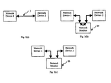
- FIGs 1(a) to 1(c) In particular, in Figure 1(a) there is shown two network devices 1,2 connected by a link 3. In Figure 1(b) there is shown an in-line connection of a network monitor 4 between the two network devices 1,2. In Figure 1(c) there is shown the connection of the network monitor 4 to the span port output 5 of a network switch or router 6. The method of gaining access to data on the network link is commonly referred to as "tapping".
- In-line tapping may be achieved using passive or active tapping methods. Both of these methods require that the insertion into the network be unobtrusive so as not to affect the transmission of data between the devices on the network.
- An active tap re-drives the network data passing though it, typically using a retimer circuit which regenerates the signal, restoring signal amplitude and timing, thus restoring signal integrity such that the ongoing signal passed back to the network is not degraded.
- an active tap may have to buffer and re-time the data in order to pass data between the two network segments.
- a passive tap does not provide for any regeneration of the signal.
- SERDES serialiser-deserialiser
- a network monitor that taps data from a network link between two network devices
- the network monitor comprising: first and second interfaces that allow the network monitor to be connected in-line in a network link between two network devices and to receive serial data therefrom and to transmit serial data thereto, each interface providing for serial-to-parallel conversion of data such that serial data received from a said network link at the interface is output as parallel data, and each interface providing for parallel-to-serial conversion of data such that parallel data received at the interface is output as serial data for transmission to a said network link; and, first and second programmable logic devices, the first programmable logic device being arranged to receive parallel data output by the first interface and to process said data for network analysis purposes, the second programmable logic device being arranged to receive parallel data output by the second interface and to process said data for network analysis purposes, each programmable logic device being controllable so as to selectively pass a copy of the received parallel data to the other programmable logic device so that the network monitor
- programmable logic devices to perform the data connection between two channels provides flexible control over the routing of the data as their programmability allows their function to be changed during normal operation. This is particularly useful as it allows the network monitor to dynamically switch between operating as an in-line or end station monitoring device.
- standard interfaces such as physical layer (PHY) ICs, are used, which provide a cost-effective method of providing an interface to allow the network monitor to be interfaced with a network link operating at several different speeds with different signalling technologies.
- PHY physical layer
- the preferred embodiment of the present invention enables active tapping of data from any serial data network protocol and particularly an Ethernet network operating at 10, 100 and 1000 Base-T with data rates of 10, 100 and 1000 Megabits per second, respectively.
- the preferred embodiment may also be applied to 10 GBase-T, operating at 10 Gbps, which has yet to be fully specified and implemented.
- the monitor comprises a first parallel data frequency and width adjuster between the first interface and the first programmable logic device, the first parallel data frequency and width adjuster being constructed and arranged to reduce the frequency and to increase the width of parallel data received from the first interface by a predetermined amount prior to said data being passed to the first programmable logic device; and, a second parallel data frequency and width adjuster between the second programmable logic device and the second interface, the second parallel data frequency and width adjuster being constructed and arranged to increase the frequency and to reduce the width of parallel data received from the second programmable logic device by said predetermined amount prior to said data being transmitted to a said network link by the second interface when the network monitor is operating in in-line mode.
- the adjusting of data frequency and width facilitates the use of low cost programmable logic devices.
- the cost of a programmable logic device is typically proportional to its speed capability and therefore, programmable logic devices that operate at lower frequencies are cheaper.
- the first parallel data frequency and width adjuster is provided by a multiplexer and the second parallel data frequency and width adjuster is provided by a demultiplexer.
- the network monitor preferably comprises a third parallel data frequency and width adjuster between the second interface and the second programmable logic device, the third parallel data frequency and width adjuster being constructed and arranged to reduce the frequency and to increase the width of parallel data received from the second interface by a predetermined amount prior to said data being passed to the second programmable logic device; and, a fourth parallel data frequency and width adjuster between the first programmable logic device and the first interface, the fourth parallel data frequency and width adjuster being constructed and arranged to increase the frequency and to reduce the width of parallel data received from the first programmable logic device by said predetermined amount prior to said data being transmitted to a said network link by the first interface when the network monitor is operating in in-line mode.
- the third parallel data frequency and width adjuster is preferably provided by a multiplexer and the fourth parallel data frequency and width adjuster is preferably provided by a demultiplexer.
- the network monitor preferably comprises a clock signal provider for providing a clock signal so that data can be clocked through the network monitor.
- the clock signal provider is constructed and arranged to obtain said clock signal by recovering a clock signal from data received at the first and second interfaces respectively.
- the use of the recovered data clock to clock the data through the network monitor from the input of one channel though to the output of the opposite channel ensures that the data and clock remain synchronised throughout the network monitor. This minimises the skew between the clock and the data. It also removes the requirement for memory based buffering between channels, therefore reducing the component count or logic requirement inside the programmable logic devices.
- each programmable logic device is a field programmable gate array.
- a method of monitoring data on a network link comprising: receiving data in serial form from a network link; converting the data in serial form to data in parallel form; passing the parallel data to a first programmable logic device for processing for network analysis purposes; controlling the first programmable logic device such that the method takes place selectively in in-line mode or in end station mode, whereby in in-line mode the first programmable logic device provides a copy of the received parallel data, the copy of the received parallel data being converted to data in serial form, said serial data being transmitted back onto the network link, and whereby in end station mode the first programmable logic device does not provide a copy of the received parallel data for conversion into serial form and transmission back onto the network link.
- the method preferably comprises, after converting the data in serial form to data in parallel form, reducing the frequency and increasing the width of the parallel data by a predetermined amount prior to said parallel data being passed to the first programmable logic device; and, when operating in in-line mode, increasing the frequency and reducing the width of the copy of the parallel data by the predetermined amount prior to the copy of the parallel data being converted to data in serial form for transmission back onto the network link.
- the method preferably comprises recovering a clock signal from the data received in serial form from the network link and using the recovered clock signal when operating in in-line mode to clock the data throughout the step of converting of the data in serial form to the data in parallel form to the step of transmitting serial data being back onto the network link.
- FIG 3(a) there is shown two network devices 1,2 connected by a link 3.
- Figure 3(b) there is shown an in-line connection of an example of a network monitor 20 according to an embodiment of the present invention between the two network devices 1,2. Once inserted, the network monitor 20 is capable of disconnecting the in-line link to enable operation in end station mode as shown in Figure 3(c).
- the network monitor 20 uses two identical circuits, referred to as Channel 1 and Channel 2, to tap data from the network.
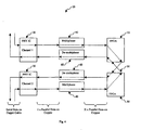
- the network monitor 20 uses pairs of four different functional blocks to implement each of these circuits as shown in Figure 4. These blocks are a physical layer IC 30, a multiplexer 40, field programmable gate array (FPGA) 50, and a de-multiplexer 60.
- FPGA field programmable gate array
- the physical layer (PHY) IC 30 provides the interface to the physical layer of the monitored network.
- the PHY IC 30 is preferably a multi-speed Ethernet PHY IC, which provides speed negotiation and signalling changes between the various speeds available on Ethernet.
- the PHY IC 30 performs serial-to-parallel conversion of the data entering the network monitor 20 from the network link.
- the PHY IC 30 also performs parallel-to-serial conversion of the data that is to be transmitted back onto the network link from the network monitor 20.
- the line-side and system-side interfaces of the PHY IC 30 may be industry standard. In practice, the PHY IC 30 may be changed to support different physical layers.
- the use of standard PHY ICs 30 provide a cost-effective method of providing an interface that allows the network monitor 20 to be interfaced with a network link operating at several different speeds with different signalling technologies.
- the multiplexer 40 interfaces the received parallel data from the PHY IC 20 to the FPGA 50.
- the multiplexer 40 applies a conversion factor X to the received data.
- the conversion factor is chosen so that the frequency of the data matches the capabilities of the chosen FPGA 50. This adjusting of the data frequency and width facilitates the use of low cost FPGAs 50.
- the cost of an FPGA is approximately proportional to its speed capability and thus FPGAs that operate at lower frequencies are cheaper. This method of decreasing the frequency by X and increasing the word width by X results in no loss of bandwidth.
- the FPGA 50 processes the data passed to it by the multiplexer 40.
- the FPGA 50 takes a copy of the data which it has been passed for processing purposes.
- the FPGA 50 passes a copy of the data to the FPGA 50 on the opposite channel if the network monitor 20 is operating in in-line mode. If required, the FPGA 50 on the opposite channel buffers the received data when the monitor 20 is operating in in-line mode. In this mode, the FPGA 50 on the opposite channel outputs the received parallel data to its associated de-multiplexer 60 for retransmission onto the network link.
- a control signal is sent to each FPGA 50 to reconfigure it such that a copy of the data received at each FPGA 50 from a channel is not passed to the other FPGA 50.
- the network monitor 20 can act as an end station for two channels simultaneously.
- FPGAs 50 or some other functionally equivalent programmable logic device, to perform the data connection between the two channels provides flexible control over the routing of the data through the network monitor 20 and thus allows the network monitor 20 to switch dynamically between in-line and end station modes. This is due to the flexibility provided by the reconfigurability of the FPGAs 50 or other programmable logic devices, allowing their function to be changed during normal operation.
- the de-multiplexer 60 interfaces the parallel data received from the FPGA 50 to the PHY IC 30.
- the conversion factor X of the de-multiplexer 60 and the multiplexer 40 should be the same to ensure that the retransmitted data rate matches the received data rate.
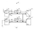
- a synchronous clock signal is used to clock the data 80 through each of the aforementioned functional blocks 30-60.
- a clock signal 70 can be provided by the PHY IC 30, which recovers a clock signal from the data 80 received from the network link. This recovered data clock, and/or its derivatives, is used to clock the data 80 through each of the four functional blocks 30-60, before clocking the data 80 into the PHY IC 30 of the opposite channel for retransmission back onto the network link.
- Figure 5 shows the flow of the clock signal 70 from Channel 1 to Channel 2 of the network monitor 20. The same arrangement is used to clock the transfer of data from Channel 2 to Channel 1.
- the frequency of the clock signal 70 may be decreased or increased by the conversion factor X as required in order to match changes in the frequency of the data 80 as it passes through each block 30-60.
- This use of the received data clock to clock the data through every stage of the network monitor 20 removes the need for re-timing the data. This is particularly valuable when the network monitor 20 is connected to a 1000 Base-T network. This arrangement minimises the skew between the clock and the data and removes the requirement for memory based buffering between channels, therefore reducing the component count or logic requirement inside the FPGAs 50.
- the flow of the clock signal 70 to the opposite channel only occurs during in-line mode.
- the clocks of the two channels are independent of each other.
Landscapes
- Engineering & Computer Science (AREA)
- Computer Networks & Wireless Communication (AREA)
- Signal Processing (AREA)
- Communication Control (AREA)
Description
- The present invention relates to a network monitor and method.
- Network monitoring systems analyse frames or packets of data as they pass through a network. The medium on which the data is carried is typically optical fibre or copper cable. The network monitor requires access to this medium in order to obtain visibility of the data passing through it. This requires the network monitor to be placed either in-line with the network link or on the span port output of a network switch or router. These connection methods are shown schematically in Figures 1(a) to 1(c). In particular, in Figure 1(a) there is shown two
network devices link 3. In Figure 1(b) there is shown an in-line connection of a network monitor 4 between the twonetwork devices span port output 5 of a network switch orrouter 6. The method of gaining access to data on the network link is commonly referred to as "tapping". - In-line tapping may be achieved using passive or active tapping methods. Both of these methods require that the insertion into the network be unobtrusive so as not to affect the transmission of data between the devices on the network. An active tap re-drives the network data passing though it, typically using a retimer circuit which regenerates the signal, restoring signal amplitude and timing, thus restoring signal integrity such that the ongoing signal passed back to the network is not degraded. Thus, an active tap may have to buffer and re-time the data in order to pass data between the two network segments. A passive tap does not provide for any regeneration of the signal.
- Active tapping of optical Gigabit Ethernet networks has been achieved using serial loopback or port-bypass features of serialiser-deserialiser (SERDES) devices in the front-end portion of the network monitor. This type of implementation is shown schematically in Figure 2. The
optical fibres 10 from the two sides of the network link are plugged into gigabit interface converters (GBICs) 11 of thenetwork monitor 3, which convert the optical data stream into high-speed serial electrical signals. These signals are passed to the SERDESdevices 12, which loop the serial data back to the opposite channel of thenetwork monitor 3, which re-drives the data back onto the network link, whilst providing a copy of the data, in parallel form, to the FPGAprogrammable devices 13 that process the data. - Although active tapping has been employed to optical network structures in manners such as that shown in Figure 2, the use of high-speed serial loopback or port bypass tends to limit the
network monitor 3 to having a fixed operation in either an in-line mode or end station mode. This is due to the need to connect and disconnect the crossover paths between the two sides of themonitor 3, to provide either a data path though themonitor 3 for in-line mode or to terminate the data path in themonitor 3 for end station mode. The constraint is due to the lack of cost-effective means to reliably switch high-speed electrical signals on the printed circuit board of themonitor 3, whilst maintaining good signal integrity. Moreover, in practice each implementation of this type of active tap architecture usually only supports one network speed, therefore limiting the scope of the product. This is typically due to the speed constraints on the serial loopback features of the SERDESdevices 12. - Passive tapping of 10 and 100 Base-T Ethernet networks, which operate on
Category 5 twisted pair copper cables, has been achieved. However, 1000 Base-T, the copper implementation of Gigabit Ethernet, has not been possible due to the signalling techniques employed on the network link. These enable simultaneous full-duplex data transmissions on each twisted pair, unlike 10 and 100 Base-T which use separate pairs for transmit and receive signals. Complex signalling techniques are also likely to be employed in the forthcoming 10 Gigabit network physical layer which will be referred to as 10 GBase-T. Therefore, an active tap is likely to be the only feasible method of accessing networks which use complex signalling techniques. - US 6 047 321, Nortel Networks, Raab et al. describes a network monitoring system working in in-line mode having a bypass relay tap being switchable between "bypass-state" and "active-state".
- According to a first aspect of the present invention, there is provided a network monitor that taps data from a network link between two network devices, the network monitor comprising: first and second interfaces that allow the network monitor to be connected in-line in a network link between two network devices and to receive serial data therefrom and to transmit serial data thereto, each interface providing for serial-to-parallel conversion of data such that serial data received from a said network link at the interface is output as parallel data, and each interface providing for parallel-to-serial conversion of data such that parallel data received at the interface is output as serial data for transmission to a said network link; and, first and second programmable logic devices, the first programmable logic device being arranged to receive parallel data output by the first interface and to process said data for network analysis purposes, the second programmable logic device being arranged to receive parallel data output by the second interface and to process said data for network analysis purposes, each programmable logic device being controllable so as to selectively pass a copy of the received parallel data to the other programmable logic device so that the network monitor can operate in in-line mode and not to pass a copy of the received parallel data to the other programmable logic device so that the network monitor can operate in end station mode, the second programmable logic device being arranged to pass the copy of the parallel data received from the first programmable logic device to the second interface for parallel-to-serial conversion and for transmission of the serial data back to a said network link when the network monitor is operating in in-line mode, the first programmable logic device being arranged to pass the copy of the parallel data received from the second programmable logic device to the first interface for parallel-to-serial conversion and for transmission of the serial data back to a said network link when the network monitor is operating in in-line mode.
- The use of programmable logic devices to perform the data connection between two channels provides flexible control over the routing of the data as their programmability allows their function to be changed during normal operation. This is particularly useful as it allows the network monitor to dynamically switch between operating as an in-line or end station monitoring device. In the preferred embodiment, standard interfaces, such as physical layer (PHY) ICs, are used, which provide a cost-effective method of providing an interface to allow the network monitor to be interfaced with a network link operating at several different speeds with different signalling technologies. The preferred embodiment of the present invention enables active tapping of data from any serial data network protocol and particularly an Ethernet network operating at 10, 100 and 1000 Base-T with data rates of 10, 100 and 1000 Megabits per second, respectively. The preferred embodiment may also be applied to 10 GBase-T, operating at 10 Gbps, which has yet to be fully specified and implemented.
- In a preferred embodiment, the monitor comprises a first parallel data frequency and width adjuster between the first interface and the first programmable logic device, the first parallel data frequency and width adjuster being constructed and arranged to reduce the frequency and to increase the width of parallel data received from the first interface by a predetermined amount prior to said data being passed to the first programmable logic device; and, a second parallel data frequency and width adjuster between the second programmable logic device and the second interface, the second parallel data frequency and width adjuster being constructed and arranged to increase the frequency and to reduce the width of parallel data received from the second programmable logic device by said predetermined amount prior to said data being transmitted to a said network link by the second interface when the network monitor is operating in in-line mode. The adjusting of data frequency and width facilitates the use of low cost programmable logic devices. The cost of a programmable logic device is typically proportional to its speed capability and therefore, programmable logic devices that operate at lower frequencies are cheaper.
- Preferably, the first parallel data frequency and width adjuster is provided by a multiplexer and the second parallel data frequency and width adjuster is provided by a demultiplexer.
- The network monitor preferably comprises a third parallel data frequency and width adjuster between the second interface and the second programmable logic device, the third parallel data frequency and width adjuster being constructed and arranged to reduce the frequency and to increase the width of parallel data received from the second interface by a predetermined amount prior to said data being passed to the second programmable logic device; and, a fourth parallel data frequency and width adjuster between the first programmable logic device and the first interface, the fourth parallel data frequency and width adjuster being constructed and arranged to increase the frequency and to reduce the width of parallel data received from the first programmable logic device by said predetermined amount prior to said data being transmitted to a said network link by the first interface when the network monitor is operating in in-line mode. The third parallel data frequency and width adjuster is preferably provided by a multiplexer and the fourth parallel data frequency and width adjuster is preferably provided by a demultiplexer.
- The network monitor preferably comprises a clock signal provider for providing a clock signal so that data can be clocked through the network monitor. Preferably, the clock signal provider is constructed and arranged to obtain said clock signal by recovering a clock signal from data received at the first and second interfaces respectively. The use of the recovered data clock to clock the data through the network monitor from the input of one channel though to the output of the opposite channel ensures that the data and clock remain synchronised throughout the network monitor. This minimises the skew between the clock and the data. It also removes the requirement for memory based buffering between channels, therefore reducing the component count or logic requirement inside the programmable logic devices.
- Preferably, each programmable logic device is a field programmable gate array.
- According to a second aspect of the present invention, there is provided a method of monitoring data on a network link, the method comprising: receiving data in serial form from a network link; converting the data in serial form to data in parallel form; passing the parallel data to a first programmable logic device for processing for network analysis purposes; controlling the first programmable logic device such that the method takes place selectively in in-line mode or in end station mode, whereby in in-line mode the first programmable logic device provides a copy of the received parallel data, the copy of the received parallel data being converted to data in serial form, said serial data being transmitted back onto the network link, and whereby in end station mode the first programmable logic device does not provide a copy of the received parallel data for conversion into serial form and transmission back onto the network link.
- The method preferably comprises, after converting the data in serial form to data in parallel form, reducing the frequency and increasing the width of the parallel data by a predetermined amount prior to said parallel data being passed to the first programmable logic device; and, when operating in in-line mode, increasing the frequency and reducing the width of the copy of the parallel data by the predetermined amount prior to the copy of the parallel data being converted to data in serial form for transmission back onto the network link.
- The method preferably comprises recovering a clock signal from the data received in serial form from the network link and using the recovered clock signal when operating in in-line mode to clock the data throughout the step of converting of the data in serial form to the data in parallel form to the step of transmitting serial data being back onto the network link.
- Embodiments of the present invention will now be described by way of example with reference to the accompanying drawings, in which:
- Figs. 1(a) to 1(c) respectively show schematically two network devices connected by a network link, an in-line connection of a network monitor between the two network devices, and the connection of the network monitor to the span port output of a network switch or router, all as known in the prior art;
- Fig. 2 shows schematically a block circuit diagram of a prior art network monitor;
- Figs. 3(a) to 3(c) respectively show schematically two network devices connected by a link, an in-line connection of an example of a network monitor according to an embodiment of the present invention between the two network devices, and operation of the network monitor in end station mode;
- Fig. 4 shows schematically a block circuit diagram of a network monitor according to an embodiment of the present invention; and,
- Fig. 5 shows schematically an example of the clocking of data through a network monitor according to an embodiment of the present invention.
- Referring now to Figure 3, in Figure 3(a) there is shown two
network devices link 3. In Figure 3(b) there is shown an in-line connection of an example of anetwork monitor 20 according to an embodiment of the present invention between the twonetwork devices network monitor 20 is capable of disconnecting the in-line link to enable operation in end station mode as shown in Figure 3(c). - Referring now to Figure 4, the
network monitor 20 uses two identical circuits, referred to as Channel 1 and Channel 2, to tap data from the network. Thenetwork monitor 20 uses pairs of four different functional blocks to implement each of these circuits as shown in Figure 4. These blocks are aphysical layer IC 30, amultiplexer 40, field programmable gate array (FPGA) 50, and a de-multiplexer 60. - The physical layer (PHY) IC 30 provides the interface to the physical layer of the monitored network. The PHY IC 30 is preferably a multi-speed Ethernet PHY IC, which provides speed negotiation and signalling changes between the various speeds available on Ethernet. The PHY IC 30 performs serial-to-parallel conversion of the data entering the
network monitor 20 from the network link. ThePHY IC 30 also performs parallel-to-serial conversion of the data that is to be transmitted back onto the network link from thenetwork monitor 20. The line-side and system-side interfaces of thePHY IC 30 may be industry standard. In practice, thePHY IC 30 may be changed to support different physical layers. The use ofstandard PHY ICs 30 provide a cost-effective method of providing an interface that allows the network monitor 20 to be interfaced with a network link operating at several different speeds with different signalling technologies. - The
multiplexer 40 interfaces the received parallel data from thePHY IC 20 to theFPGA 50. Themultiplexer 40 applies a conversion factor X to the received data. In particular, themultiplexer 40 decreases the frequency of the data by X times and also increases the width of the data words by X times. For example, if data is transmitted into themultiplexer 40 where X=2, then 10-bit words at a frequency of 125 MHz are output as 20-bit words at a frequency of 62.5 MHz. The conversion factor is chosen so that the frequency of the data matches the capabilities of the chosenFPGA 50. This adjusting of the data frequency and width facilitates the use oflow cost FPGAs 50. The cost of an FPGA is approximately proportional to its speed capability and thus FPGAs that operate at lower frequencies are cheaper. This method of decreasing the frequency by X and increasing the word width by X results in no loss of bandwidth. - The
FPGA 50 processes the data passed to it by themultiplexer 40. TheFPGA 50 takes a copy of the data which it has been passed for processing purposes. TheFPGA 50 passes a copy of the data to theFPGA 50 on the opposite channel if the network monitor 20 is operating in in-line mode. If required, theFPGA 50 on the opposite channel buffers the received data when themonitor 20 is operating in in-line mode. In this mode, theFPGA 50 on the opposite channel outputs the received parallel data to its associatedde-multiplexer 60 for retransmission onto the network link. - When the
monitor 20 is not operating in in-line mode, a control signal is sent to eachFPGA 50 to reconfigure it such that a copy of the data received at eachFPGA 50 from a channel is not passed to theother FPGA 50. In this way, the network monitor 20 can act as an end station for two channels simultaneously. - The use of
FPGAs 50, or some other functionally equivalent programmable logic device, to perform the data connection between the two channels provides flexible control over the routing of the data through thenetwork monitor 20 and thus allows the network monitor 20 to switch dynamically between in-line and end station modes. This is due to the flexibility provided by the reconfigurability of theFPGAs 50 or other programmable logic devices, allowing their function to be changed during normal operation. - When the network monitor 20 is operating in in-line mode, the de-multiplexer 60 interfaces the parallel data received from the
FPGA 50 to thePHY IC 30. The de-multiplexer 60 increases the frequency of the data by X times and decreases the width of the data words by X times. For example, if data is transmitted into the de-multiplexer 60 where X=2, then 20-bit words at a frequency of 62.5 MHz are output to the PHY IC as 10-bit words at a frequency of 125 MHz. This method of increasing the frequency by X and decreasing the word width by X results in no loss of bandwidth. - The conversion factor X of the de-multiplexer 60 and the
multiplexer 40 should be the same to ensure that the retransmitted data rate matches the received data rate. - In a preferred embodiment, a synchronous clock signal is used to clock the
data 80 through each of the aforementioned functional blocks 30-60. Aclock signal 70 can be provided by thePHY IC 30, which recovers a clock signal from thedata 80 received from the network link. This recovered data clock, and/or its derivatives, is used to clock thedata 80 through each of the four functional blocks 30-60, before clocking thedata 80 into thePHY IC 30 of the opposite channel for retransmission back onto the network link. Figure 5 shows the flow of theclock signal 70 fromChannel 1 toChannel 2 of thenetwork monitor 20. The same arrangement is used to clock the transfer of data fromChannel 2 toChannel 1. The frequency of theclock signal 70 may be decreased or increased by the conversion factor X as required in order to match changes in the frequency of thedata 80 as it passes through each block 30-60. This use of the received data clock to clock the data through every stage of the network monitor 20 removes the need for re-timing the data. This is particularly valuable when the network monitor 20 is connected to a 1000 Base-T network. This arrangement minimises the skew between the clock and the data and removes the requirement for memory based buffering between channels, therefore reducing the component count or logic requirement inside theFPGAs 50. - The flow of the
clock signal 70 to the opposite channel only occurs during in-line mode. When the network monitor 20 is operating in end station mode, the clocks of the two channels are independent of each other. - Embodiments of the present invention have been described with particular reference to the examples illustrated. However, it will be appreciated that variations and modifications may be made to the examples described within the scope of the present invention, which is limited by the appended claims. For example, the multiplexer and
de-multiplexer blocks
Claims (11)
- A network monitor (20) that taps data from a network link between two network devices, the network monitor comprising:first and second interfaces (30) that allow the network monitor (20) to be connected in-line in a network link between two network devices and to receive serial data therefrom and to transmit serial data thereto, each interface providing for serial-to-parallel conversion of data such that serial data received from a said network link at the interface (30) is output as parallel data, and each interface (30) providing for parallel-to-serial conversion of data such that parallel data received at the interface (30) is output as serial data for transmission to a said network link; and,first and second programmable logic devices (50),the first programmable logic device (50) being arranged to receive parallel data output by the first interlace (30) and to process said data for network analysis purposes, the second programmable logic device (50) being arranged to receive parallel data output by the second interface (30) and to process said data for network analysis purposes, each programmable logic device (50) being controllable so as to selectively pass a copy of the received parallel data to the other programmable logic device (50) so that the network monitor (20) can operate in in-line mode and not to pass a copy of the received parallel data to the other programmable logic device (50) so that the network monitor (20) can operate in end station mode,the second programmable logic device (50) being arranged to pass the copy of the parallel data received from the first programmable logic device (50) to the second interface (30) for parallel-to-serial conversion and for transmission of the serial data back to a said network link when the network monitor (20) is operating in in-line mode,the first programmable logic device (50) being arranged to pass the copy of the parallel data received from the second programmable logic devices (50) to the first interfaced (30) for parallel-to-serial conversion and for transmission of the serial data back to a said network link when the network monitor (20) is operating in in-line mode.
- A network monitor (20) according to claim 1, comprising:a first parallel data frequency and width adjuster between the first interface (30) and the first programmable logic device (50), the first parallel data frequency and width adjuster being constructed and arranged to reduce the frequency and to increase the width of parallel data (80) received from the first interface (30) by a predetermined amount prior to said data (80) being passed to the first programmable logic device (50); and,a second parallel data frequency and width adjuster between the second programmable logic device (50) and the second interface (30), the second parallel data frequency and width adjuster being constructed and arranged to increase the frequency and to reduce the width of parallel data (80) received from the second programmable logic device (50) by said predetermined amount prior to said data (80) being transmitted to a said network link by the second interface (30) when the network monitor (20) is operating in in-line mode.
- A network monitor (20) according to claim 2, wherein the first parallel data frequency and width adjuster is provided by a multiplexer (40) and the second parallel data frequency and width adjuster is provided by a demultiplexer (60).
- A network monitor (20) according to claim 2 or claim 3, comprising:a third parallel data frequency and width adjuster between the second interfaced (30) and the second programmable logic device (50), the third parallel data frequency and width adjuster being constructed and arranged to reduce the frequency and to increase the width of parallel data (80) received from the second interface (30) by a predetermined amount prior to said data (80) being passed to the second programmable logic device (50); and,a fourth parallel data frequency and width adjuster between the first programmable logic device (50) and the first interface (30), the fourth parallel data frequency and width adjuster being constructed and arranged to increase the frequency and to reduce the width of parallel data (80) received from the first programmable logic device (50) by said predetermined amount prior to said data (80) being transmitted to a said network link by the first interface (30) when the network monitor (20) is operating in in-line mode.
- A network monitor (20) according to claim 4, wherein the third parallel data frequency and width adjuster is provided by a multiplexer (40) and the fourth parallel,data frequency and width adjuster is provided by a demultiplexer (60).
- A network monitor (20) according to any of claims 1 to 5, comprising a clock signal provider for providing a clock signal (70) so that data (80) can be clocked through the network monitor.
- A network monitor (20) according to claim 6, wherein the clock signal provider is constructed and arranged to obtain said clock signal (70) by recovering a clock signal from data (80) received at the first and second interfaces (30) respectively.
- A network monitor (20) according to any of claims 1 to 7, wherein each programmable logic device (50) is a field programmable gate array.
- A method of monitoring data on a network link, the method comprising:receiving data in serial form from a network link;converting the data in serial form to data in parallel form;passing the parallel data to a first programmable logic device (50) for processing for network analysis purposes;controlling the first programmable logic device (50) such that the method takes place selectively in in-line mode or in end station mode,whereby in in-line mode the first programmable logic device (50) provides a copy of the received parallel data (80), the copy of the received parallel data (80) being converted to data in serial form, said serial data being transmitted back onto the network link, and
whereby in end station mode the first programmable logic device (50) does not provide a copy of the received parallel data (80) for conversion into serial form and transmission back onto the network link. - A method according to claim 9, comprising:after converting the data (80) in serial form to data in parallel form, reducing the frequency and increasing the width of the parallel data by a predetermined amount prior to said parallel data (80) being passed to the first programmable logic device (50); and,when operating in in-line mode, increasing the frequency and reducing the width of the copy of the parallel data (80) by the predetermined amount prior to the copy of the parallel data (80) being converted to data in serial form for transmission back onto the network link.
- A method according to claim 9 or claim 10, comprising recovering a clock signal from the data received in serial form from the network link and using the recovered clock signal when operating in in-line mode to clock the data throughout the step of converting of the data in serial form to the data in parallel form to the step of transmitting serial data being back onto the network link.
Applications Claiming Priority (3)
| Application Number | Priority Date | Filing Date | Title |
|---|---|---|---|
| US40270402P | 2002-08-13 | 2002-08-13 | |
| US402704P | 2002-08-13 | ||
| PCT/GB2003/003210 WO2004015921A1 (en) | 2002-08-13 | 2003-07-30 | Network monitor and method |
Publications (2)
| Publication Number | Publication Date |
|---|---|
| EP1529373A1 EP1529373A1 (en) | 2005-05-11 |
| EP1529373B1 true EP1529373B1 (en) | 2007-04-11 |
Family
ID=31715885
Family Applications (1)
| Application Number | Title | Priority Date | Filing Date |
|---|---|---|---|
| EP03784232A Expired - Fee Related EP1529373B1 (en) | 2002-08-13 | 2003-07-30 | Network monitor and method |
Country Status (5)
| Country | Link |
|---|---|
| US (1) | US7411946B2 (en) |
| EP (1) | EP1529373B1 (en) |
| AU (1) | AU2003248951A1 (en) |
| DE (1) | DE60313179T2 (en) |
| WO (1) | WO2004015921A1 (en) |
Families Citing this family (19)
| Publication number | Priority date | Publication date | Assignee | Title |
|---|---|---|---|---|
| US7613837B2 (en) * | 2003-03-31 | 2009-11-03 | Gordy Stephen C | Network tap with interchangeable ports |
| US7281167B2 (en) * | 2003-08-26 | 2007-10-09 | Finisar Corporation | Multi-purpose network diagnostic modules |
| US20050129033A1 (en) * | 2003-12-13 | 2005-06-16 | Gordy Stephen C. | Network tap for use with multiple attached devices |
| US8565095B2 (en) * | 2005-04-19 | 2013-10-22 | Alcatel Lucent | Context controlled data tap utilizing parallel logic for integrated link monitoring |
| CN101411124A (en) * | 2006-02-14 | 2009-04-15 | 菲尼萨公司 | Diagnostic functions in an in-line device |
| US8576731B2 (en) * | 2006-02-14 | 2013-11-05 | Jds Uniphase Corporation | Random data compression scheme in a network diagnostic component |
| US8607145B2 (en) * | 2006-02-14 | 2013-12-10 | Jds Uniphase Corporation | Show OOB and speed negotiation data graphically in a network diagnostic component |
| US7673184B2 (en) * | 2006-02-14 | 2010-03-02 | Jds Uniphase Corporation | Flow control methodology for digital retiming devices |
| US8769152B2 (en) | 2006-02-14 | 2014-07-01 | Jds Uniphase Corporation | Align/notify compression scheme in a network diagnostic component |
| US8125906B2 (en) * | 2006-03-03 | 2012-02-28 | Kiranmai Vedanabhatla | Capture RCDT and SNTT SAS speed negotiation decodes in a network diagnostic component |
| WO2008110198A1 (en) * | 2007-03-09 | 2008-09-18 | Mentor Graphics Corporation | Hardware interface board for connecting an emulator to a network |
| US7792046B2 (en) * | 2008-06-05 | 2010-09-07 | Vss Monitoring, Inc. | Ethernet switch-based network monitoring system and methods |
| US20100290354A1 (en) * | 2009-05-15 | 2010-11-18 | Vss Monitoring, Inc. | Method for determining ethernet mode of operation during passive monitoring |
| US10503690B2 (en) * | 2018-02-23 | 2019-12-10 | Xilinx, Inc. | Programmable NOC compatible with multiple interface communication protocol |
| US10658079B1 (en) | 2019-08-18 | 2020-05-19 | Medigate tech Ltd. | Crowd-based recommendations of a version of firmware for medical devices |
| US10600512B1 (en) | 2019-08-18 | 2020-03-24 | Medigate tech Ltd. | Network-based calculation of prevalence of repeated medical imaging |
| US11056232B2 (en) | 2019-08-18 | 2021-07-06 | Medigate tech Ltd. | Medication usage auditing based on analysis of infusion pump network traffic |
| US10825566B1 (en) | 2019-08-18 | 2020-11-03 | Medigate tech Ltd. | Ensuring availability of medical devices to receive maintenance |
| CN114268674A (en) * | 2020-09-15 | 2022-04-01 | 西安诺瓦星云科技股份有限公司 | Video processing equipment and video pre-monitoring method |
Family Cites Families (6)
| Publication number | Priority date | Publication date | Assignee | Title |
|---|---|---|---|---|
| US4064360A (en) * | 1976-07-06 | 1977-12-20 | The United States Of America As Represented By The Secretary Of The Navy | High speed digital switch |
| EP0661848B1 (en) | 1993-12-28 | 2001-09-05 | NEC Corporation | Monitor and control system for communications equipment |
| US5548590A (en) | 1995-01-30 | 1996-08-20 | Hewlett-Packard Company | High performance frame time monitoring system and method for a fiber optic switch for a fiber optic network |
| US6047321A (en) | 1996-02-23 | 2000-04-04 | Nortel Networks Corporation | Method and apparatus for monitoring a dedicated communications medium in a switched data network |
| US5864486A (en) * | 1996-05-08 | 1999-01-26 | Lattice Semiconductor Corporation | Method and apparatus for in-system programming of a programmable logic device using a two-wire interface |
| US6888800B1 (en) | 1998-11-14 | 2005-05-03 | Emulex Design & Manufacturing Corporation | High performance digital loop diagnostic technology |
-
2003
- 2003-07-30 AU AU2003248951A patent/AU2003248951A1/en not_active Abandoned
- 2003-07-30 US US10/524,528 patent/US7411946B2/en active Active
- 2003-07-30 DE DE60313179T patent/DE60313179T2/en not_active Expired - Fee Related
- 2003-07-30 EP EP03784232A patent/EP1529373B1/en not_active Expired - Fee Related
- 2003-07-30 WO PCT/GB2003/003210 patent/WO2004015921A1/en active IP Right Grant
Non-Patent Citations (1)
| Title |
|---|
| None * |
Also Published As
| Publication number | Publication date |
|---|---|
| DE60313179D1 (en) | 2007-05-24 |
| DE60313179T2 (en) | 2007-12-27 |
| AU2003248951A1 (en) | 2004-02-25 |
| WO2004015921A1 (en) | 2004-02-19 |
| US7411946B2 (en) | 2008-08-12 |
| US20060153177A1 (en) | 2006-07-13 |
| EP1529373A1 (en) | 2005-05-11 |
Similar Documents
| Publication | Publication Date | Title |
|---|---|---|
| EP1529373B1 (en) | Network monitor and method | |
| US7362797B2 (en) | Physical layer device having an analog SERDES pass through mode | |
| US6424627B1 (en) | Full-duplex medium tap apparatus and system | |
| US6754238B1 (en) | Method and apparatus for transport of control information over a data link | |
| WO2001086878A2 (en) | System and process for embedded cable modem in a cable modem termination system to enable diagnostics and monitoring | |
| US9143464B2 (en) | Method and system for speed negotiation for twisted pair links using intelligent E-FIFO in fibre channel systems | |
| CN101616048A (en) | The multiport Ethernet transceiver | |
| US7555574B2 (en) | Asymmetric data path media access controller | |
| US11646959B2 (en) | Active ethernet cable with broadcasting and multiplexing for data path redundancy | |
| US20010003484A1 (en) | Optical line protection device and optical line protection method | |
| US9729472B2 (en) | Network physical link (PHY) switch system | |
| WO2021061348A1 (en) | Complementary data flow for noise reduction | |
| CA2408496A1 (en) | System and process for return channel spectrum manager | |
| WO2003081785A1 (en) | Physcial layer device having an analog serdes pass through mode | |
| CN114050865B (en) | Data transmission device, chip and electronic equipment | |
| US20060010336A1 (en) | Connection apparatus and method for network testers and analysers | |
| Iniewski et al. | SerDes technology for gigabit I/O communications in storage area networking | |
| US7266624B1 (en) | Programmable layered sub-system interface | |
| JP2001007833A (en) | Interface converter |
Legal Events
| Date | Code | Title | Description |
|---|---|---|---|
| PUAI | Public reference made under article 153(3) epc to a published international application that has entered the european phase |
Free format text: ORIGINAL CODE: 0009012 |
|
| 17P | Request for examination filed |
Effective date: 20050210 |
|
| AK | Designated contracting states |
Kind code of ref document: A1 Designated state(s): AT BE BG CH CY CZ DE DK EE ES FI FR GB GR HU IE IT LI LU MC NL PT RO SE SI SK TR |
|
| AX | Request for extension of the european patent |
Extension state: AL LT LV MK |
|
| DAX | Request for extension of the european patent (deleted) | ||
| RBV | Designated contracting states (corrected) |
Designated state(s): DE FR GB |
|
| GRAP | Despatch of communication of intention to grant a patent |
Free format text: ORIGINAL CODE: EPIDOSNIGR1 |
|
| GRAS | Grant fee paid |
Free format text: ORIGINAL CODE: EPIDOSNIGR3 |
|
| GRAA | (expected) grant |
Free format text: ORIGINAL CODE: 0009210 |
|
| RIN1 | Information on inventor provided before grant (corrected) |
Inventor name: CARTER, BRIAN, R. Inventor name: WIDLEY, GARRY Inventor name: WORRALL, A.C. |
|
| AK | Designated contracting states |
Kind code of ref document: B1 Designated state(s): DE FR GB |
|
| REG | Reference to a national code |
Ref country code: GB Ref legal event code: FG4D |
|
| REF | Corresponds to: |
Ref document number: 60313179 Country of ref document: DE Date of ref document: 20070524 Kind code of ref document: P |
|
| ET | Fr: translation filed | ||
| PLBE | No opposition filed within time limit |
Free format text: ORIGINAL CODE: 0009261 |
|
| STAA | Information on the status of an ep patent application or granted ep patent |
Free format text: STATUS: NO OPPOSITION FILED WITHIN TIME LIMIT |
|
| 26N | No opposition filed |
Effective date: 20080114 |
|
| PG25 | Lapsed in a contracting state [announced via postgrant information from national office to epo] |
Ref country code: DE Free format text: LAPSE BECAUSE OF NON-PAYMENT OF DUE FEES Effective date: 20080201 |
|
| REG | Reference to a national code |
Ref country code: FR Ref legal event code: ST Effective date: 20080331 |
|
| PG25 | Lapsed in a contracting state [announced via postgrant information from national office to epo] |
Ref country code: FR Free format text: LAPSE BECAUSE OF NON-PAYMENT OF DUE FEES Effective date: 20070731 |
|
| PGFP | Annual fee paid to national office [announced via postgrant information from national office to epo] |
Ref country code: GB Payment date: 20080520 Year of fee payment: 6 |
|
| GBPC | Gb: european patent ceased through non-payment of renewal fee |
Effective date: 20090730 |
|
| PG25 | Lapsed in a contracting state [announced via postgrant information from national office to epo] |
Ref country code: GB Free format text: LAPSE BECAUSE OF NON-PAYMENT OF DUE FEES Effective date: 20090730 |