EP1500638B1 - Laser irradiated metallised electroceramic - Google Patents
Laser irradiated metallised electroceramic Download PDFInfo
- Publication number
- EP1500638B1 EP1500638B1 EP03405554A EP03405554A EP1500638B1 EP 1500638 B1 EP1500638 B1 EP 1500638B1 EP 03405554 A EP03405554 A EP 03405554A EP 03405554 A EP03405554 A EP 03405554A EP 1500638 B1 EP1500638 B1 EP 1500638B1
- Authority
- EP
- European Patent Office
- Prior art keywords
- electroceramic
- metallization
- irradiated
- manufacturing
- varistor
- Prior art date
- Legal status (The legal status is an assumption and is not a legal conclusion. Google has not performed a legal analysis and makes no representation as to the accuracy of the status listed.)
- Expired - Lifetime
Links
Images

Classifications
-
- C—CHEMISTRY; METALLURGY
- C04—CEMENTS; CONCRETE; ARTIFICIAL STONE; CERAMICS; REFRACTORIES
- C04B—LIME, MAGNESIA; SLAG; CEMENTS; COMPOSITIONS THEREOF, e.g. MORTARS, CONCRETE OR LIKE BUILDING MATERIALS; ARTIFICIAL STONE; CERAMICS; REFRACTORIES; TREATMENT OF NATURAL STONE
- C04B41/00—After-treatment of mortars, concrete, artificial stone or ceramics; Treatment of natural stone
- C04B41/009—After-treatment of mortars, concrete, artificial stone or ceramics; Treatment of natural stone characterised by the material treated
-
- C—CHEMISTRY; METALLURGY
- C04—CEMENTS; CONCRETE; ARTIFICIAL STONE; CERAMICS; REFRACTORIES
- C04B—LIME, MAGNESIA; SLAG; CEMENTS; COMPOSITIONS THEREOF, e.g. MORTARS, CONCRETE OR LIKE BUILDING MATERIALS; ARTIFICIAL STONE; CERAMICS; REFRACTORIES; TREATMENT OF NATURAL STONE
- C04B41/00—After-treatment of mortars, concrete, artificial stone or ceramics; Treatment of natural stone
- C04B41/45—Coating or impregnating, e.g. injection in masonry, partial coating of green or fired ceramics, organic coating compositions for adhering together two concrete elements
- C04B41/50—Coating or impregnating, e.g. injection in masonry, partial coating of green or fired ceramics, organic coating compositions for adhering together two concrete elements with inorganic materials
- C04B41/51—Metallising, e.g. infiltration of sintered ceramic preforms with molten metal
-
- C—CHEMISTRY; METALLURGY
- C04—CEMENTS; CONCRETE; ARTIFICIAL STONE; CERAMICS; REFRACTORIES
- C04B—LIME, MAGNESIA; SLAG; CEMENTS; COMPOSITIONS THEREOF, e.g. MORTARS, CONCRETE OR LIKE BUILDING MATERIALS; ARTIFICIAL STONE; CERAMICS; REFRACTORIES; TREATMENT OF NATURAL STONE
- C04B41/00—After-treatment of mortars, concrete, artificial stone or ceramics; Treatment of natural stone
- C04B41/80—After-treatment of mortars, concrete, artificial stone or ceramics; Treatment of natural stone of only ceramics
- C04B41/81—Coating or impregnation
- C04B41/85—Coating or impregnation with inorganic materials
- C04B41/88—Metals
-
- H—ELECTRICITY
- H01—ELECTRIC ELEMENTS
- H01C—RESISTORS
- H01C7/00—Non-adjustable resistors formed as one or more layers or coatings; Non-adjustable resistors made from powdered conducting material or powdered semi-conducting material with or without insulating material
- H01C7/10—Non-adjustable resistors formed as one or more layers or coatings; Non-adjustable resistors made from powdered conducting material or powdered semi-conducting material with or without insulating material voltage responsive, i.e. varistors
- H01C7/105—Varistor cores
- H01C7/108—Metal oxide
-
- C—CHEMISTRY; METALLURGY
- C04—CEMENTS; CONCRETE; ARTIFICIAL STONE; CERAMICS; REFRACTORIES
- C04B—LIME, MAGNESIA; SLAG; CEMENTS; COMPOSITIONS THEREOF, e.g. MORTARS, CONCRETE OR LIKE BUILDING MATERIALS; ARTIFICIAL STONE; CERAMICS; REFRACTORIES; TREATMENT OF NATURAL STONE
- C04B2111/00—Mortars, concrete or artificial stone or mixtures to prepare them, characterised by specific function, property or use
- C04B2111/00474—Uses not provided for elsewhere in C04B2111/00
- C04B2111/00844—Uses not provided for elsewhere in C04B2111/00 for electronic applications
-
- Y—GENERAL TAGGING OF NEW TECHNOLOGICAL DEVELOPMENTS; GENERAL TAGGING OF CROSS-SECTIONAL TECHNOLOGIES SPANNING OVER SEVERAL SECTIONS OF THE IPC; TECHNICAL SUBJECTS COVERED BY FORMER USPC CROSS-REFERENCE ART COLLECTIONS [XRACs] AND DIGESTS
- Y10—TECHNICAL SUBJECTS COVERED BY FORMER USPC
- Y10T—TECHNICAL SUBJECTS COVERED BY FORMER US CLASSIFICATION
- Y10T29/00—Metal working
- Y10T29/49—Method of mechanical manufacture
- Y10T29/49002—Electrical device making
- Y10T29/49082—Resistor making
Definitions
- the invention relates to the field of electrical engineering, in particular to electroceramic components, such as varistors. It relates to a method for producing an electroceramic component according to the preamble of claim 1.
- Electroceramic components are ceramic components which can be electrically contacted and subjected to an electrical voltage in order to fulfill an electrical, electromechanical or other function. Its essential component is an electroceramic. Examples of electroceramic components are high-temperature superconductor components, piezocrystalline components, ceramic capacitors, hot and cold conductors, ceramic resistors, ceramic gas sensors and varistors. The latter will be discussed in more detail below.
- Varistors are electroceramic components with a non-linear current-voltage characteristic, which are mainly used as arresters in medium-voltage high-voltage, but also low-voltage range.
- Metal oxide varistors based on sintered varistor ceramics, for example based on doped ZnO, are predominantly used.
- the contacts For contacting such and other electroceramics are generally provided with two (or more) metallic electrodes, the contacts must have a low contact resistance and high current carrying capacity. In addition, it requires a strong adhesion of the metal layer on the ceramic surface to ensure a secure and mechanically stable contact.
- US 6,169,038 discloses a method of roughening a surface of a semiconductor in which the surface is etched with an acid. By the etching process, a micro-roughness of the surface can be generated. If a surface roughened in this way is provided with a metallization, a strong interlocking between the semiconductor and the metal layer results due to the microroughness, so that a good adhesion between the metal layer and the semiconductor surface is reached. Similar etching techniques are used in the manufacture of varistors and other electroceramic devices.
- metallization is applied to at least one surface part of a sintered electroceramic body.
- the method is characterized in that the surface portion is irradiated with laser light prior to the application of the metallization.
- Another significant advantage of laser irradiation is that the shape of the (surface part to be metallized) can be selected in a simple manner and virtually as desired. For example, in wet chemical processes, masks must be attached to the electroceramic body to form parts of the electrochemical body Exclude the surface of the electroceramic body from the treatment. In the laser irradiation, the laser beam can be easily controlled so that only the surface part to be metallized is irradiated. Thus, metallizations (electrodes) can be produced in a simple manner, covering a defined area, a defined part, of the electroceramic body.
- the adhesion of the metallization on the electroceramic body is increased by the laser treatment, well-defined electrode shapes can be produced in particular also with metallization processes which-at least without the use of masks-do not permit metallization which can be limited well to a limited surface area (for example metal deposition from the gas phase or electrochemical metal deposition).
- a limited surface area for example metal deposition from the gas phase or electrochemical metal deposition.
- the adhesion of the deposited metal is then lower than on the surface part, so that the metal there is easily removable from the electroceramic body, for example by brushing.
- the adhesion of the metal on the non-laser-irradiated surface areas is so small that there is no deposition, so no metallization takes place.
- the electroceramic body has two outer surfaces, which are separated by at least one edge, wherein each of these two outer surfaces is to be provided with at least one metallization (electrode), and it is provided that a voltage is applied between these two electrodes, which is easy producibility of defined surface parts to be metallized advantageous.
- at least one of the surface portions may be selected (and metallized) to be spaced from the edge. There is then at least one between the edge and the surface part arranged edge. In this way, the probability of electrical flashover from one electrode to the other is reduced compared to the case where the metallization extended to the edge.
- Both metallizations (electrodes) preferably have an edge.
- the laser irradiation can have the advantage that not only flat (planar), but also curved surfaces can be processed in a simple manner, for example a surface on a cylinder jacket.
- the surface part for roughening the surface part can be irradiated with the laser light.
- a roughening serves a particularly good anchoring of the metallization on the electroceramic body.
- Such roughnesses achieved have lateral expansions of typically between 0.1 .mu.m and 50 .mu.m, usually between 2 .mu.m and 20 .mu.m, and vertical expansions of typically between 0.1 .mu.m and 10 .mu.m, usually between 0.3 .mu.m and 5 .mu.m. It can a particularly good adhesion and peel strength of the metallization can be achieved. An increased roughness is achieved.
- the surface portion is irradiated with the laser light prior to applying the metallization to improve the adhesion of the metallization by modifying the chemical nature of the surface portion.
- the chemical composition of the surface of the electroceramic body can be changed by laser irradiation, for example by changing the stoichiometry of oxides at the surface. Due to the modified chemical composition of the surface part, the adhesion of the metallization can be further improved.
- the surface part can be irradiated with the laser light to increase the electrical transverse conductivity of the surface part.
- the surface of a sintered electroceramic body usually has substantially the same electrical properties as the volume of the sintered electroceramic body.
- a transverse conductivity is desirable.
- the transverse conductivity which results from the current-voltage ratio in the case of two electrodes arranged on the surface part at a distance, can be significantly reduced by the laser irradiation, in particular by several orders of magnitude.
- the transverse conductivity resulting from the current-voltage ratio in the case of two on the surface part spaced apart electrodes can be significantly reduced by the laser irradiation, in particular by at least one or two or at least seven to nine orders of magnitude, depending on voltage applied to the varistor. Only a thin surface area plays a role for the transverse conductivity.
- the electroceramic (the varistor) has thereby more favorable electrical properties and improved contactability.
- the contact resistance can be significantly reduced.
- the surface part has a ripple after sintering of the ceramic body.
- Such ripples or deformations have lateral dimensions of typically between 50 ⁇ m and 30 mm, usually between 100 ⁇ m and 10 mm, and vertical dimensions of typically between 5 ⁇ m and 500 ⁇ m, usually between 10 ⁇ m and 200 ⁇ m.
- varistors are often contacted under high mechanical pressure: two advantageously on opposite sides of the Varistors arranged metallizations is each a contacting plate, typically made of aluminum, pressed to ensure good electrical contact. If now the waviness (before the laser irradiation) is large, there will be a mechanical and electrical contact between the contacting plate and metallization only at relatively few and relatively widely spaced contact points on the surface part. This results in the contact pressure of Konktakt michsplatten to a very inhomogeneous force into the varistor (Elektrokeramik emotions). In addition, in the case of current surges (current pulses), pressure surges (mechanical pressure waves) occur at the contact points, which are the greater the fewer contact points exist.
- the use of laser radiation for the pretreatment of a varistor ceramic / an electroceramic for the application of a metallization can significantly increase the service life of the varistor / of the electroceramic component. It is achieved a homogeneous current distribution and a homogeneous pressure distribution over the entire metallized surface part. Analogous problems are solved in the case of other electroceramics by the laser irradiation before the metallization.
- a focused laser beam is used as the laser light.
- the surface part is irradiated with a focused laser beam before the application of the metallization to reduce the waviness of the surface part, whereby a particularly good and efficient leveling of the surface portion is achieved.
- the energy density of the laser beam can be maximized in this way near the surface of the electroceramic body, while further inside the ceramic body (below the surface) there is a reduced energy density and thus less influence on the ceramic material.
- the laser beam is focused on a surface which is arranged parallel to a surface which conveys the waviness of the surface part. As a result, a particularly good leveling and thus a particularly low waviness of the surface part is achieved.
- a further particularly preferred embodiment is characterized in that an energy deposited in the surface part per unit area by means of the laser beam is used to level a surface part curved before the laser irradiation depending on the location on the surface part. If the energy deposited in the surface part by the laser beam per unit area is to be selected depending on the location on the surface part, this can be made advantageous by a light power of the laser beam and / or a beam diameter of the laser beam and / or the laser beam per unit time irradiated area and / or a number of exposures to which a partial surface of the surface portion is exposed, depending on the location selected on the surface portion.
- the laser beam can then drive, for example, several times over areas to be planarized and / or run off in adjacent regions narrower grid lines and / or descend the grid lines slower and / or with greater light intensity.
- the ceramic is advantageously measured in order to determine the extent of the shape deviation and the correspondingly required laser intensity. It is achieved a location-dependent material removal on the surface part. In particular, larger ripples or deviations in shape can be corrected than the use of a focused laser beam without location-dependent removal rate allowed.
- the electroceramic body has a grain structure, and on the surface part loose grains and / or grain composites of the electroceramic body are exhibited, and / or cracks in the grain structure grains and / or grain composites of the electroceramic body are exhibited.
- the surface portion is irradiated with laser light prior to the application of the metallization for the removal of such grains and / or grain composites.
- Typical linear dimensions of such grains in varistors are between 10 ⁇ m and several 100 ⁇ m.
- defects such as cracks can be introduced into the ceramic body, in particular into the uppermost grain layers.
- the uppermost layer of a surface part then often consists of a loose grain composite, whereby the adhesion of the metallization is lowered.
- Such loose or arranged on cracks grains or grain composites can be removed by means of laser radiation, so that a good, homogeneous electrical and mechanical contact (high tensile strength) between ceramic and metallization is achieved.
- an electroceramic article is stored on a sinter pad during sintering with at least a portion of the surface portion. It may happen that components of the sintering substrate remain in the surface part after completion of the sintering process.
- components of the sintering substrate remain in the surface part after completion of the sintering process.
- by irradiating the surface portion with laser light prior to application of the metallization such constituents of the sintering substrate can be removed.
- a homogeneous nature of the surface portion is achieved, which is free from caused by such components of the sintered substrate local differences in electrical properties.
- the electroceramic body Before or after the application of the metallization, the electroceramic body can be at least partially provided with a non-conductive passivation layer. If such a passivation layer is applied before the application of the metallization, it may happen that parts of the passivation layer are located on the surface part. In this case, it is preferable to irradiate the surface portion with laser light before depositing the metallization to ablate such portions of the passivation layer located on the surface portion. Large and inhomogeneous contact resistances between metallization and electroceramic bodies, which would result from such parts of the passivation layer, are avoided so that uniform electrical properties and low resistance between metallization and electroceramic body are achieved.
- the electroceramic component can be, for example, a varistor or a high-temperature superconductor component or a piezoceramic component or a ceramic capacitor or a hot or a PTC or a ceramic resistor or a ceramic gas sensor.
- the electroceramic component is a varistor and the electroceramic body is a varistor body
- the varistor body is preferably a doped sintered metal oxide ceramic, preferably based on ZnO, SnO 2 SrTiO 3 or TiO 2 , or a doped carbide ceramic, for example SiC.
- the surface portion of a varistor body can be irradiated with laser light to reduce a voltage dependency of the transverse conductivity of the surface portion with great advantage.
- a varistor-like voltage dependence of the transverse conductivity that is present before the laser irradiation can be converted into an (almost) ohmic characteristic curve.
- the surface of a sintered ceramic body generally has substantially the same electrical properties as the volume of the sintered ceramic body.
- a highly non-linear current-voltage characteristic with high electrical resistance at voltages below the switching voltage (breakdown voltage) of the varistor is exhibited.
- the strong voltage dependence of the transverse conductivity of the surface part can be reduced so far that a substantially linear, so ohmic characteristic is exhibited.
- a varistor-like, strongly non-linear dependence of a current flowing in the surface part of an applied voltage is after the laser irradiation a substantially ohmic characteristic of the transverse conductivity before (in a thin surface area).
- the varistor thus has more favorable electrical properties and improved contactability.
- the electroceramic body is substantially cylindrical, disk-shaped or plate-shaped, wherein on the two mutually parallel boundary surfaces of the cylinder or the disc or the plate depending a surface portion is arranged, on which two surface portions each a metallization is applied.
- the application of the metallization is preferably carried out by thermal spraying.
- the electroceramic body is substantially tubular or cylindrical, wherein a metallization is applied to two mutually axially spaced, substantially annular, arranged on the outer surface of the tube or cylinder surface parts.
- the application of the metallization is preferably carried out by thermal spraying.
- this is used as a pretreatment for applying a metallization to an electroceramic, in particular to a varistor ceramic.
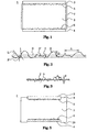
- Fig. 1 shows schematically a section through a varistor 1 produced according to the invention as an example of an electroceramic component.
- the varistor is substantially cylindrically shaped and has a varistor body 2.
- the top and bottom surfaces of the cylinder form surface portions 5 and 6, respectively, which are provided with metallizations 3 and 4, respectively.
- the non-metallized cylindrical peripheral surface is provided with a passivation layer 7.
- the varistor 1 is preferably used for overvoltage protection in the high voltage, medium voltage or low voltage range.
- General background on varistors and the preferably used materials are, for example, the book " Ceramic Transaction, Vol. 3, Editor: LM Levinson, American Ceramic Society, 1988 or the publication DR Clarke, Varistor Ceramics, J. Am. Ceram. Soc, 82 (1999), pp. 485-502 removable.
- General background on the subject of electroceramics and the materials preferably used are, for example, the book “Ceramic Materials for Electronics", Editor: Relva C. Buchanan, Electrical Engineering and Eletronics / 31, 1986 removable.
- the varistor body 2 is a sintered ceramic, preferably based on a metal oxide, in particular ZnO.
- the varistor body 2 contains further elements as doping, for example Bi, Sb, Co, Mn, Cr.
- the varistor body 2 is formed in one piece.
- the metallizations 3, 4 are used to make contact with the varistor body 2 and thus form electrodes 3, 4.
- the metallizations 3, 4 should have a high current-carrying capacity and a low contact resistance with the ceramic 2. In addition, they should have a good adhesion to the ceramic (high tensile strength).
- the metallizations 3,4 are preferably made of Al, Zn, Cu, Ag or alloys such as brass.
- the metallizations 3, 4 are applied to the surface parts 5 and 6, respectively. In Fig. 1 However, they may also be larger and include the bottom or top surface or be smaller and may be included from the bottom or top surface. In Fig. 1 the metallizations 3, 4 are arranged completely on the surface parts 5, 6.
- the passivation layer 7 is non-conductive and preferably vitreous, ceramic or a polymer.
- the constituents of the varistor ceramic 2 are mixed in powder form, pressed and then sintered on a sintered substrate at temperatures of typically between 900 ° C. and 1500 ° C. After that, a mechanical rough cleaning of the varistor ceramic 2 can be carried out, for example by brushing.
- each surface segment is irradiated only once; but it is also possible and may be advantageous to irradiate two or more times the same area segment.
- the area irradiated with the laser can be controlled electronically or computer-aided, even complex geometries can be generated and complex-shaped varistor bodies can be processed.
- rectangular-shaped electrodes and electrodes can be realized on a lateral surface of a tubular or cylindrical varistor body, which extend, for example, along a circumference of the varistor body (see, for example Fig. 6 ).
- a focused laser beam is used.
- Typical focal lengths are between 10 mm and 800 mm, preferably between 50 mm and 250 mm.
- Fig. 2 schematically shows a section through a sintered varistor body 2 before the laser irradiation.
- the laser beam L is indicated with its focal point F.
- the illustrated surface portion 5 has a waviness, which are mainly due to impressions of the sintered substrate.
- This waviness typically has a lateral dimension ⁇ of the order of magnitude of 10 ⁇ m to several millimeters and a typical vertical dimension D of the order of magnitude of 10 ⁇ m to 0.5 mm.
- Fig. 2 is by means of the thin line drawn over the surface part 5 (shown by thick line), illustrates that a sintered varistor body surface generally also has a certain (microscopic) roughness.
- a surface which conveys the waviness of the surface part 5 is in Fig. 2 designated as S.
- the surface S is a flat surface. Due to a desired homogeneity of the electric field in the varistor body 2, a planar shape of the electrodes 3, 4 generally becomes preferably, so that the surface S is preferably flat.
- Particularly suitable for reducing the vertical dimension of the waviness is when the focus F of the laser beam L is guided in such a way that it always lies in a surface S 'parallel to the surface S.
- the surface S ' is advantageously arranged on the volume of the varistor body 2 facing side of the surface S, preferably with a distance of 0.1 mm to 2 mm.
- the use of a focused laser beam results in a depth-dependent energy density and ablation performance of the laser beam.
- Fig. 3 shows schematically in section an enlarged section of a surface part 5 according to Fig. 2 , after the laser irradiation.
- the ripple is virtually eliminated. This results in very homogeneous field distributions and a uniform current distribution.
- the surface part 5 has a roughness.
- This micro-roughness typically has a lateral dimension of the order of 1 ⁇ m to 10 ⁇ m and a vertical dimension of the order of 1 ⁇ m.
- the microroughness causes a good adhesion of the metallization on the lasered surface portion 5.
- Preferably produced microroughness R a be 1 micron to 4 microns and are thus the usual, generated by etching micro roughness of typically 1 micron to 1.5 micron depth equivalent or even significantly superior.
- the laser irradiation is used primarily for the pretreatment of the varistor ceramic 2 for the subsequent metallization.
- the metallizations 3, 4 are preferably applied to the surface parts 5, 6 by means of thermal spraying, for example by arc spraying.
- thermal spraying for metal coatings applied by thermal spraying, sufficient roughness of the surface to be metallized is particularly important since the adhesion is essentially mechanical and not or hardly chemically conditioned.
- Other metallization processes such as PVD, sputtering, electrochemical deposition or screen printing, are also possible.
- an area can be laser irradiated, of which then only a part (namely, the surface part 5 or 6) is metallized.
- the entire bottom or top surface can be lasered, which are then only partially provided with the metallizations 3,4.
- the passivation layer 7 is advantageously applied before or after the application of the metallizations 3, 4. It represents an insulation layer. If the passivation layer 7 is applied before the application of the metallizations 3, 4, non-conductive, glassy or polymeric residues can thereby reach the surface parts 5, 6. Such residues, which could lead to inhomogeneities of the electric field and electrical breakdowns can be removed by the laser irradiation.
- Fig. 4 are current-voltage characteristics double-logarithmic, which were measured by means of two on a non-laser-irradiated surface part (circles and squares) and on a laser-irradiated surface part (triangles and diamonds) of a Varistor body applied electrodes.
- the voltage V applied between the electrodes is plotted against the current I flowing between the electrodes.
- the distance between the electrodes was 3 mm for the squares and the data represented by diamonds.
- the electrode spacing was 4 mm.
- Fig. 5 serves to further illustrate the invention and shows a similar varistor 1 as Fig. 1 , That's why Fig. 5 starting from Fig. 1 described.
- the varistor 1 in Fig. 1 take the electrodes 3,4 in Fig. 5 not the entire top or bottom surface of the cylinder, but only a part, so that in each case one of the surface parts 5 and 6 adjacent edge 9 or 10 results.
- the edges 9 and 10 reduce the likelihood of electrical flashover.
- the metallizations 3,4 as in the example of Fig. 1 until the edge of the cylinder jacket extending from the top or bottom surface of the cylinder, then an electric flashover between the two metallizations would be at a applied voltage much more likely than with the edges 9,10 off Fig. 5 ,
- the metallization 3 of the surface part 5 is so thick that it projects beyond the edge 9. This results in an easier contactability by means of a contact piece (not shown), which is at least approximately as large as the surface portion. 5
- the adhesion of the metallization 3 is increased by the laser irradiation on the surface part 5. If metal is able to adhere to the edge 9 at all during the metallization, then it adheres significantly less there than the metal on the surface part 5. As a result, any metal deposited on the edge 9 can simply be removed so that an electrode geometry defined by the laser irradiation is produced ,
- the surface portion 6 is, unlike the surface portion 5, provided with such a thin metallization 4 that it is surmounted by the edge 10. As a result, the edge 10 forms an (additional) barrier against electrical breakdown.
- Etching processes have the disadvantage that the ceramic bodies are placed in an etching bath and therefore the entire ceramic is etched, ie both surface parts to be metallized and surface parts which are not to be metallized. This can be the electrical properties of the ceramic influence negatively. Covering non-metallized surface parts during the etching is difficult and expensive. The laser irradiation does not need such masks.
- Fig. 6 shows an example of non-planar electrodes 3,4.
- the illustrated electroceramic component 1 (for example varistor 1 or piezoceramic 1) has a tubular ceramic body 2.
- the electrodes 3, 4 are arranged on the outer lateral surface 8 of the tube and are annular, the lateral surface 8 enclosing.
- the laser irradiation such as well as more complex shaped surface parts are treatable.
- the laser treatment in air or in another gas atmosphere takes place. This can influence the conductivity and chemical composition of the irradiated surface part.
Landscapes
- Chemical & Material Sciences (AREA)
- Engineering & Computer Science (AREA)
- Ceramic Engineering (AREA)
- Structural Engineering (AREA)
- Materials Engineering (AREA)
- Organic Chemistry (AREA)
- Microelectronics & Electronic Packaging (AREA)
- Inorganic Chemistry (AREA)
- Electromagnetism (AREA)
- Physics & Mathematics (AREA)
- Thermistors And Varistors (AREA)
- Ceramic Products (AREA)
- Apparatuses And Processes For Manufacturing Resistors (AREA)
- Fixed Capacitors And Capacitor Manufacturing Machines (AREA)
- Coating By Spraying Or Casting (AREA)
- Ceramic Capacitors (AREA)
Abstract
Description
Die Erfindung bezieht sich auf das Gebiet der Elektrotechnik, insbesondere auf elektrokeramische Bauteile, wie zum Beispiel Varistoren. Sie bezieht sich auf ein Verfahren zur Herstellung eines elektrokeramischen Bauteils gemäss dem Oberbegriff des Patentanspruches 1.The invention relates to the field of electrical engineering, in particular to electroceramic components, such as varistors. It relates to a method for producing an electroceramic component according to the preamble of
Elektrokeramische Bauteile sind keramische Bauteile, die elektrisch kontaktierbar und mit einer elektrischen Spannung beaufschlagbar sind, um eine elektrische, elektromechanische oder sonstige Funktion zu erfüllen. Ihr wesentlicher Bestandteil ist eine Elektrokeramik. Beispiele für elektrokeramische Bauteile sind Hochtemperatursupraleiterbauteile, piezokristalline Bauteile, keramische Kondensatoren, Heiss- und Kaltleiter, keramische Widerstände, keramische Gassensoren und Varistoren. Auf letztere wird im folgenden genauer eingegangen.Electroceramic components are ceramic components which can be electrically contacted and subjected to an electrical voltage in order to fulfill an electrical, electromechanical or other function. Its essential component is an electroceramic. Examples of electroceramic components are high-temperature superconductor components, piezocrystalline components, ceramic capacitors, hot and cold conductors, ceramic resistors, ceramic gas sensors and varistors. The latter will be discussed in more detail below.
Varistoren sind elektrokeramische Bauteile mit einer nichtlinearen Strom-Spannungskennlinie, die vor allem als Ableiter in Mittelspannungs-Hochspannungs-, aber auch Niederspannungsbereich eingesetzt werden. Es werden vorwiegend Metalloxid-Varistoren eingesetzt, die auf gesinterten Varistorkeramiken, beispielsweise auf der Grundlage von dotiertem ZnO, basieren. Zur Kontaktierung werden solche und andere Elektrokeramiken im allgemeinen mit zwei (oder mehr) metallischen Elektroden versehen, wobei die Kontakte einen geringen Übergangswiderstand und eine hohe Stromtragfähigkeit aufweisen müssen. Zudem bedarf es einer starken Haftung der Metallschicht auf der Keramikoberfläche, um einen sicheren und mechanisch stabilen Kontakt zu gewährleisten.Varistors are electroceramic components with a non-linear current-voltage characteristic, which are mainly used as arresters in medium-voltage high-voltage, but also low-voltage range. Metal oxide varistors based on sintered varistor ceramics, for example based on doped ZnO, are predominantly used. For contacting such and other electroceramics are generally provided with two (or more) metallic electrodes, the contacts must have a low contact resistance and high current carrying capacity. In addition, it requires a strong adhesion of the metal layer on the ceramic surface to ensure a secure and mechanically stable contact.
In
In US 6'169'038 ist ein Verfahren zur Aufrauhung einer Oberfläche eines Halbleiters offenbart, in welchem die Oberfläche mit einer Säure geätzt wird. Durch den Ätzprozess kann eine Mikrorauhigkeit der Oberfläche erzeugt werden. Wird eine solcherart aufgerauhte Oberfläche mit einer Metallisierung versehen, so ergibt sich aufgrund der Mikrorauhigkeit eine starke Verzahnung zwischen dem Halbleiter und der Metallschicht, so dass eine gute Haftung zwischen der Metallschicht und der Halbleiteroberfläche erreicht wird. Ähnliche Ätzverfahren finden bei der Herstellung von Varistoren und anderen elektrokeramischen Bauteilen Anwendung.US 6,169,038 discloses a method of roughening a surface of a semiconductor in which the surface is etched with an acid. By the etching process, a micro-roughness of the surface can be generated. If a surface roughened in this way is provided with a metallization, a strong interlocking between the semiconductor and the metal layer results due to the microroughness, so that a good adhesion between the metal layer and the semiconductor surface is reached. Similar etching techniques are used in the manufacture of varistors and other electroceramic devices.
Bei derartigen Ätzverfahren fallen zu entsorgende chemische Abfälle an, und bei der Durchführung solcher Verfahren müssen aufgrund der Gefährlichkeit der eingesetzten Chemikalien aufwendige Sicherheitsmassnahmen getroffen werden.In such etching process to be disposed of chemical waste, and in the implementation of such methods complex safety measures must be taken due to the danger of the chemicals used.
Es ist deshalb Aufgabe der Erfindung, ein Verfahren der eingangs genannten Art zu schaffen, welches die oben genannten Nachteile nicht aufweist. Durch das erfindungsgemässe Verfahren soll insbesondere eine sichere und umweltfreundliche Metallisierung einer Elektrokeramik ermöglicht werden.It is therefore an object of the invention to provide a method of the type mentioned, which does not have the disadvantages mentioned above. The method according to the invention is intended, in particular, to enable a safe and environmentally friendly metallization of an electroceramics.
Diese Aufgabe löst ein Verfahren mit den Merkmalen des Patentanspruches 1.This object is achieved by a method having the features of
Weiter wird in Patentanspruch 17 eine Verwendung von Laserlicht beansprucht.Furthermore, a use of laser light is claimed in claim 17.
In dem erfindungsgemässen Verfahren zur Herstellung eines elektrokeramischen Bauteils wird auf mindestens einen Oberflächenteil eines gesinterten Elektrokeramikkörpers eine Metallisierung aufgebracht. Das Verfahren kennzeichnet sich dadurch, dass vor dem Aufbringen der Metallisierung der Oberflächenteil mit Laserlicht bestrahlt wird.In the method according to the invention for producing an electroceramic component, metallization is applied to at least one surface part of a sintered electroceramic body. The method is characterized in that the surface portion is irradiated with laser light prior to the application of the metallization.
Dadurch können andere Verfahren zur Bearbeitung des Oberflächenteils, wie Ätzen, Schleifen, Sandstrahlen oder spanabhebende Verfahren durch die Bestrahlung mittels Laserlichtes ersetzt werden, welches ein umweltfreundliches und schnelles Verfahren ist. Zudem ist durch die Laserbestrahlung eine besonders vorteilhafte Beschaffenheit des Oberflächenteils erzeugbar.As a result, other methods of processing the surface portion, such as etching, grinding, sand blasting, or machining processes, can be replaced by the laser light irradiation, which is an environmentally friendly and rapid process. In addition, a particularly advantageous nature of the surface part can be generated by the laser irradiation.
Ein weiterer, bedeutender Vorteil der Laserbestrahlung ist es, dass die Form des (zu metallisierenden) Oberflächenteils auf einfache Weise und praktisch beliebig wählbar ist. Bei nasschemischen Verfahren beispielsweise müssen Masken an dem Elektrokeramikkörper angebracht werden, um Teile der Oberfläche des Elektrokeramikkörpers von der Behandlung auszuschliessen. Bei der Laserbestrahlung kann der Laserstrahl einfach so gesteuert werden, dass nur der zu metallisierende Oberflächenteil bestrahlt wird. So können auf einfache Weise Metallisierungen (Elektroden) erzeugt werden, die eine definierte Fläche, einen definierten Teil, des Elektrokeramikkörpers bedecken.Another significant advantage of laser irradiation is that the shape of the (surface part to be metallized) can be selected in a simple manner and virtually as desired. For example, in wet chemical processes, masks must be attached to the electroceramic body to form parts of the electrochemical body Exclude the surface of the electroceramic body from the treatment. In the laser irradiation, the laser beam can be easily controlled so that only the surface part to be metallized is irradiated. Thus, metallizations (electrodes) can be produced in a simple manner, covering a defined area, a defined part, of the electroceramic body.
Insbesondere wenn durch die Laserbehandlung die Haftung der Metallisierung auf dem Elektrokeramikkörper erhöht wird, können wohldefinierte Elektrodenformen insbesondere auch mit Metallisierungsverfahren erzeugt werden, die - zumindest ohne einen Einsatz von Masken - keine gut auf einen begrenzten Oberflächenbereich eingrenzbare Metallisierung erlauben (zum Beispiel Metallabscheidung aus der Gasphase oder elektrochemische Metallabscheidung). In den nicht laserbestrahlten Oberflächenbereichen ist die Haftung des abgeschiedenen Metalls dann geringer als auf dem Oberflächenteil, so dass das Metall dort einfach von dem Elektrokeramikkörper entfernbar ist, beispielsweise durch Bürsten. Oder die Haftung des Metalls auf den nicht laserbestrahlten Oberflächenbereichen ist so gering, dass dort keine Abscheidung, also keine Metallisierung stattfindet.In particular, if the adhesion of the metallization on the electroceramic body is increased by the laser treatment, well-defined electrode shapes can be produced in particular also with metallization processes which-at least without the use of masks-do not permit metallization which can be limited well to a limited surface area (for example metal deposition from the gas phase or electrochemical metal deposition). In the non-laser-irradiated surface areas, the adhesion of the deposited metal is then lower than on the surface part, so that the metal there is easily removable from the electroceramic body, for example by brushing. Or the adhesion of the metal on the non-laser-irradiated surface areas is so small that there is no deposition, so no metallization takes place.
Insbesondere wenn der Elektrokeramikkörper zwei Aussenflächen aufweist, die durch mindestens eine Kante voneinander getrennt sind, wobei jede dieser zwei Aussenflächen mit mindestens einer Metallisierung (Elektrode) zu versehen ist, und wobei vorgesehen ist, dass zwischen diesen zwei Elektroden eine Spannung angelegt wird, ist die einfache Erzeugbarkeit von definierten zu metallisierenden Oberflächenteilen vorteilhaft. Dann kann nämlich zumindest einer der Oberflächenteile so gewählt werden (und metallisiert werden), dass er zu der Kante beabstandet ist. Es gibt dann mindestens einen zwischen der Kante und dem Oberflächenteil angeordneten Rand. Auf diese Weise wird die Wahrscheinlichkeit eines elektrischen Überschlags von der einen zu der anderen Elektrode verringert gegenüber dem Fall, dass die Metallisierung sich bis an die Kante erstreckte. Bevorzugt weisen beide Metallisierungen (Elektroden) einen Rand auf.In particular, if the electroceramic body has two outer surfaces, which are separated by at least one edge, wherein each of these two outer surfaces is to be provided with at least one metallization (electrode), and it is provided that a voltage is applied between these two electrodes, which is easy producibility of defined surface parts to be metallized advantageous. Namely, at least one of the surface portions may be selected (and metallized) to be spaced from the edge. There is then at least one between the edge and the surface part arranged edge. In this way, the probability of electrical flashover from one electrode to the other is reduced compared to the case where the metallization extended to the edge. Both metallizations (electrodes) preferably have an edge.
Eine weitere Verbesserung der Überschlagsfestigkeit wird erreicht, wenn durch die Laserbestrahlung in dem Oberflächenteil Material der Elektrokeramik abgetragen wird, und wenn der Elektrokeramikkörper nach der Laserbestrahlung einen an den Oberflächenteil angrenzenden Rand aufweist, welcher Rand nicht oder weniger als der Oberflächenteil mit dem Laserlicht bestrahlt wird. Nach der Laserbestrahlung grenzt dann also ein nicht (oder weniger) laserbestrahlter Rand an den Oberflächenteil an, welcher gegenüber dem Oberflächenteil erhaben ist. Der Rand überragt den Oberflächenteil und kann die Wahrscheinlichkeit von elektrischen Überschlägen über den Rand hinweg verringern, insbesondere wenn die Metallisierung auch von dem Rand überragt wird.Further improvement in flashover resistance is achieved when material of the electroceramic material is ablated by the laser irradiation in the surface portion, and when the electroceramic body has an edge adjacent to the surface portion after the laser irradiation, which edge is not or less than the surface portion irradiated with the laser light. After the laser irradiation, a non-irradiated (or less) laser-irradiated edge then adjoins the surface part, which is raised in relation to the surface part. The edge projects beyond the surface portion and can reduce the likelihood of electrical flashover over the edge, especially if the metallization is also surmounted by the edge.
Gegenüber anderen Verfahren zur Vorbereitung des Oberflächenteils für die Metallisierung kann die Laserbestrahlung den Vorteil haben, dass auf einfache Weise nicht nur ebene (planare), sondern auch gekrümmte Flächen bearbeitet werden können, beispielsweise eine Fläche auf einem Zylindermantel.Compared with other methods for preparing the surface part for the metallization, the laser irradiation can have the advantage that not only flat (planar), but also curved surfaces can be processed in a simple manner, for example a surface on a cylinder jacket.
Besonders vorteilhaft kann der Oberflächenteil zur Aufrauhung des Oberflächenteils mit dem Laserlicht bestrahlt werden. Eine solche Aufrauhung dient einer besonders guten Verankerung der Metallisierung auf dem Elektrokeramikkörper. Derartig erzielte Rauhigkeiten weisen laterale Ausdehnungen von typischerweise zwischen 0.1 µm und 50 µm, meist zwischen 2 µm und 20 µm, und vertikale Ausdehnungen von typischerweise zwischen 0.1 µm und 10 µm, meist zwischen 0.3 µm und 5 µm, auf. Es kann eine besonders gute Haftung und Abzugsfestigkeit der Metallisierung erreicht werden. Eine erhöhte Rauhigkeit wird erreicht.Particularly advantageously, the surface part for roughening the surface part can be irradiated with the laser light. Such a roughening serves a particularly good anchoring of the metallization on the electroceramic body. Such roughnesses achieved have lateral expansions of typically between 0.1 .mu.m and 50 .mu.m, usually between 2 .mu.m and 20 .mu.m, and vertical expansions of typically between 0.1 .mu.m and 10 .mu.m, usually between 0.3 .mu.m and 5 .mu.m. It can a particularly good adhesion and peel strength of the metallization can be achieved. An increased roughness is achieved.
Mit Vorteil wird der Oberflächenteil vor dem Aufbringen der Metallisierung zur Verbesserung der Haftung der Metallisierung durch Modifikation der chemischen Beschaffenheit des Oberflächenteils mit dem Laserlicht bestrahlt. Ähnlich wie bei Ätzverfahren kann durch eine Laserbestrahlung die chemische Zusammensetzung der Oberfläche des Elektrokeramikkörpers verändert werden, beispielsweise durch Änderung der Stöchiometrie von Oxiden an der Oberfläche. Durch die modifizierte chemische Zusammensetzung des Oberflächenteils kann die Haftung der Metallisierung noch verbessert werden.Advantageously, the surface portion is irradiated with the laser light prior to applying the metallization to improve the adhesion of the metallization by modifying the chemical nature of the surface portion. Similar to etching methods, the chemical composition of the surface of the electroceramic body can be changed by laser irradiation, for example by changing the stoichiometry of oxides at the surface. Due to the modified chemical composition of the surface part, the adhesion of the metallization can be further improved.
Mit grossem Vorteil kann der Oberflächenteil zur Vergrösserung der elektrischen Querleitfähigkeit des Oberflächenteils mit dem Laserlicht bestrahlt werden.With great advantage, the surface part can be irradiated with the laser light to increase the electrical transverse conductivity of the surface part.
Die Oberfläche eines gesinterten Elektrokeramikkörpers hat zumeist im wesentlichen die gleichen elektrischen Eigenschaften wie das Volumen des gesinterten Elektrokeramikkörpers. Für einen geringen Kontaktwiderstand ist aber oftmals eine grössere Querleitfähigkeit wünschenswert. Die Querleitfähigkeit, welche sich aus dem Strom-Spannungs-Verhältnis im Falle zweier auf dem Oberflächenteil beabstandet angebrachten Elektroden ergibt, kann durch die Laserbestrahlung deutlich, insbesondere um mehrere Grössenordnungen verringert werden.The surface of a sintered electroceramic body usually has substantially the same electrical properties as the volume of the sintered electroceramic body. For a low contact resistance but often a larger transverse conductivity is desirable. The transverse conductivity, which results from the current-voltage ratio in the case of two electrodes arranged on the surface part at a distance, can be significantly reduced by the laser irradiation, in particular by several orders of magnitude.
Im Falle eines Varistors liegt ein sehr grosser elektrischer Widerstand insbesondere bei Spannungen unterhalb der Schaltspannung des Varistors (Durchbruchspannung) vor. Die Querleitfähigkeit, welche sich aus dem Strom-Spannungs-Verhältnis im Falle zweier auf dem Oberflächenteil beabstandet angebrachten Elektroden ergibt, kann durch die Laserbestrahlung deutlich, insbesondere um mindestens eine oder zwei oder bis zu mindestens sieben bis neun Grössenordnungen verringert werden, abhängig von am Varistor anliegenden Spannung. Für die Querleitfähigkeit spielt nur ein dünner Oberflächenbereich eine Rolle.In the case of a varistor, there is a very high electrical resistance, in particular at voltages below the switching voltage of the varistor (breakdown voltage). The transverse conductivity, resulting from the current-voltage ratio in the case of two on the surface part spaced apart electrodes can be significantly reduced by the laser irradiation, in particular by at least one or two or at least seven to nine orders of magnitude, depending on voltage applied to the varistor. Only a thin surface area plays a role for the transverse conductivity.
Auf diese Weise wird ein geringer Übergangswiderstand von der Metallisierung zum Elektrokeramikkörper (Varistorkörper) erzielt. Die Elektrokeramik (der Varistor) weist dadurch günstigere elektrische Eigenschaften und eine verbesserte Kontaktierbarkeit auf. Der Kontaktwiderstand kann deutlich reduziert werden.In this way, a low contact resistance from the metallization to the electroceramic body (varistor body) is achieved. The electroceramic (the varistor) has thereby more favorable electrical properties and improved contactability. The contact resistance can be significantly reduced.
Meistens weist der Oberflächenteil nach dem Sintern des Keramikkörpers eine Welligkeit auf. Das heisst, dass der Oberflächenteil Deformationen aufweist. Derartige Welligkeiten oder Deformationen weisen laterale Ausdehnungen von typischerweise zwischen 50 µm und 30 mm, meist zwischen 100 µm und 10 mm, und vertikale Ausdehnungen von typischerweise zwischen 5 µm und 500 µm, meist zwischen 10 µm und 200 µm, auf. Durch die Bestrahlung mit dem Laserlicht vor dem Aufbringen der Metallisierung kann diese Welligkeit des Oberflächenteils verringert werden, das heisst, dass die vertikale Ausdehnung der Unebenheiten oder Welligkeiten verringert wird. Der Oberflächenteil wird geglättet.Most of the surface part has a ripple after sintering of the ceramic body. This means that the surface part has deformations. Such ripples or deformations have lateral dimensions of typically between 50 μm and 30 mm, usually between 100 μm and 10 mm, and vertical dimensions of typically between 5 μm and 500 μm, usually between 10 μm and 200 μm. By irradiation with the laser light prior to application of the metallization, this waviness of the surface portion can be reduced, that is, the vertical extent of the unevenness or undulation is reduced. The surface part is smoothed.
Dadurch werden verbesserte elektrische und mechanische Eigenschaften des elektrokeramischen Bauteils erzielt, da eine homogenere Verteilung des elektrischen Feldes, des Stromflusses und mechanischer (Druck-) Belastungen erreicht wird.As a result, improved electrical and mechanical properties of the electroceramic component are achieved because a more homogeneous distribution of the electric field, the current flow and mechanical (pressure) loads is achieved.
Beispielsweise werden Varistoren oft unter grossem mechanischen Druck kontaktiert: Auf zwei vorteilhaft auf einander gegenüberliegenden Seiten des Varistors angeordnete Metallisierungen wird je eine Kontaktierungsplatte, typischerweise aus Aluminium, gepresst, um einen guten elektrischen Kontakt zu gewährleisten. Wenn die nun die Welligkeit (vor der Laserbestrahlung) gross ist, wird es einen mechanischen und elektrischen Kontakt zwischen Kontaktierungsplatte und Metallisierung nur an relativ wenigen und relativ weit beabstandeten Kontaktpunkten auf dem Oberflächenteil geben. Dadurch kommt es bei dem Anpressdruck der Konktaktierungsplatten zu einer sehr inhomogenen Krafteinleitung in den Varistorkörper (Elektrokeramikkörper). Ausserdem entstehen bei Stromstössen (Strompulsen) Druckstösse (mechanische Druckwellen) an den Kontaktpunkten, die umso grösser sind, je weniger Kontaktpunkte existieren. Und zudem führen Stromstösse zu lokaler Erwärmung an den Kontaktpunkten. Jedes der drei genannten Phänomene führt im allgemeinen rasch zur Ausbildung von Rissen in der Keramik. Die Risse sind meist oberflächennah und finden ihren Anfangspunkt im allgemeinen nahe den (wenigen) Kontaktpunkten. Solche Risse degradieren den elektrischen und mechanischen Kontakt zwischen Metallisierung und Keramik sowie den Varistorkörper. Wird die Keramik vor dem Aufbringen der Metallisierung in geeigneter Weise mit Laserlicht bestrahlt, so kann die Welligkeit (vor allem in ihrer vertikalen Dimension) deutlich verringert werden, so dass eine deutlich grössere Zahl und Dichte von Kontaktpunkten vorliegt. Entsprechend kann die Verwendung von Laserstrahlung zur Vorbehandlung einer Varistorkeramik / einer Elektrokeramik für das Aufbringen einer Metallisierung die Standzeit des Varistors / des elektrokeramischen Bauteils deutlich velängern. Es wird eine homogene Stromverteilung und eine homogene Druckverteilung über den gesamten metallisierten Oberflächenteil erreicht. Analoge Probleme werden im Falle anderer Elektrokeramiken durch die Laserbestrahlung vor der Metallisierung gelöst.For example, varistors are often contacted under high mechanical pressure: two advantageously on opposite sides of the Varistors arranged metallizations is each a contacting plate, typically made of aluminum, pressed to ensure good electrical contact. If now the waviness (before the laser irradiation) is large, there will be a mechanical and electrical contact between the contacting plate and metallization only at relatively few and relatively widely spaced contact points on the surface part. This results in the contact pressure of Konktaktierungsplatten to a very inhomogeneous force into the varistor (Elektrokeramikkörper). In addition, in the case of current surges (current pulses), pressure surges (mechanical pressure waves) occur at the contact points, which are the greater the fewer contact points exist. And moreover, surges lead to local heating at the contact points. Each of the three mentioned phenomena generally leads rapidly to the formation of cracks in the ceramic. The cracks are mostly close to the surface and generally find their starting point close to the (few) contact points. Such cracks degrade the electrical and mechanical contact between metallization and ceramic as well as the varistor body. If the ceramic is suitably irradiated with laser light before the application of the metallization, the waviness (especially in its vertical dimension) can be significantly reduced, so that a significantly greater number and density of contact points is present. Accordingly, the use of laser radiation for the pretreatment of a varistor ceramic / an electroceramic for the application of a metallization can significantly increase the service life of the varistor / of the electroceramic component. It is achieved a homogeneous current distribution and a homogeneous pressure distribution over the entire metallized surface part. Analogous problems are solved in the case of other electroceramics by the laser irradiation before the metallization.
In einer besonders bevorzugten Variante des Herstellungsverfahrens wird als das Laserlicht ein fokussierter Laserstrahl eingesetzt. Insbesondere wird der Oberflächenteil vor dem Aufbringen der Metallisierung zur Verringerung der Welligkeit des Oberflächenteils mit einem fokussierten Laserstrahl bestrahlt, wodurch eine besonders gute und effiziente Einebnung des Oberflächenteils erreicht wird. Die Energiedichte des Laserstrahls kann auf diese Weise nahe der Oberfläche des Elektrokeramikkörpers maximiert werden, während weiter im Inneren des Keramikkörpers (unterhalb der Oberfläche) eine verringerte Energiedichte und somit eine geringere Beeinflussung des Keramikmaterials vorliegt. Insbesondere wird der Laserstrahl auf eine Fläche fokussiert wird, die parallel zu einer die Welligkeit des Oberflächenteils ausmittelnden Fläche angeordnet ist. Dadurch wird eine besonders gute Einebnung und somit eine besonders geringe Welligkeit des Oberflächenteils erzielt.In a particularly preferred variant of the production method, a focused laser beam is used as the laser light. In particular, the surface part is irradiated with a focused laser beam before the application of the metallization to reduce the waviness of the surface part, whereby a particularly good and efficient leveling of the surface portion is achieved. The energy density of the laser beam can be maximized in this way near the surface of the electroceramic body, while further inside the ceramic body (below the surface) there is a reduced energy density and thus less influence on the ceramic material. In particular, the laser beam is focused on a surface which is arranged parallel to a surface which conveys the waviness of the surface part. As a result, a particularly good leveling and thus a particularly low waviness of the surface part is achieved.
Eine weitere besonders bevorzugte Ausführungsform kennzeichnet sich dadurch, dass eine mittels des Laserstrahls pro Flächeneinheit in dem Oberflächenteil deponierte Energie zur Einebnung eines vor der Laserbestrahlung gekrümmten Oberflächenteils abhängig vom Ort auf dem Oberflächenteil gewählt wird.
Wenn die mittels des Laserstrahls pro Flächeneinheit in dem Oberflächenteil deponierte Energie abhängig vom Ort auf dem Oberflächenteil gewählt wird werden soll, kann dies vorteilhaft gemacht werden, indem eine Lichtleistung des Laserstrahls und/oder ein Strahldurchmesser des Laserstrahls und/oder die pro Zeiteinheit von dem Laserstrahl bestrahlte Fläche und/oder eine Anzahl von Bestrahlungen, denen eine Teilfläche des Oberflächenteils ausgesetzt wird, abhängig vom Ort auf dem Oberflächenteil gewählt wird.A further particularly preferred embodiment is characterized in that an energy deposited in the surface part per unit area by means of the laser beam is used to level a surface part curved before the laser irradiation depending on the location on the surface part.
If the energy deposited in the surface part by the laser beam per unit area is to be selected depending on the location on the surface part, this can be made advantageous by a light power of the laser beam and / or a beam diameter of the laser beam and / or the laser beam per unit time irradiated area and / or a number of exposures to which a partial surface of the surface portion is exposed, depending on the location selected on the surface portion.
Dadurch können unerwünschte Formabweichungen mit einer vertikalen Ausdehnung der Grössenordnung von typischerweise 0.1 mm bis 3 mm beseitigt oder zumindest deutlich verringert werden. Der Laserstrahl kann dann zum Beispiel mehrfach über einzuebnende Bereiche fahren und/oder in einzuebnenden Bereichen enger benachbarte Rasterlinien abfahren und/oder die Rasterlinien langsamer und/oder mit grösserer Lichtintensität abfahren. Vor der Laserbestrahlung oder während der Laserbestrahlung wird die Keramik vorteilhaft vermessen, um das Mass der Formabweichung und die entsprechend erforderliche Laserintensität zu bestimmen. Es wird ein ortsabhängiger Materialabtrag an dem Oberflächenteil erreicht. Insbesondere können auch grössere Welligkeiten oder Formabweichungen korrigiert werden als es der Einsatz eines fokussierten Laserstrahles ohne ortsabhängige Abtragungsrate erlaubte.This can cause unwanted shape deviations with a vertical extent of the order of typically 0.1 mm to 3 mm eliminated or at least significantly reduced. The laser beam can then drive, for example, several times over areas to be planarized and / or run off in adjacent regions narrower grid lines and / or descend the grid lines slower and / or with greater light intensity. Before the laser irradiation or during the laser irradiation, the ceramic is advantageously measured in order to determine the extent of the shape deviation and the correspondingly required laser intensity. It is achieved a location-dependent material removal on the surface part. In particular, larger ripples or deviations in shape can be corrected than the use of a focused laser beam without location-dependent removal rate allowed.
In einer weiteren vorteilhaften Ausführungsform der Erfindung weist der Elektrokeramikkörper eine Kornstruktur auf, und an dem Oberflächenteil werden lose Körner und/oder Kornverbünde des Elektrokeramikkörpers aufgewiesen, und/oder an Rissen in der Kornstruktur werden Körner und/oder Kornverbünde des Elektrokeramikkörpers aufgewiesen. Der Oberflächenteil wird vor dem Aufbringen der Metallisierung zur Abtragung solcher Körner und/oder Kornverbünde mit Laserlicht bestrahlt. Typische Lineardimension solcher Körner in Varistoren liegen zwischen 10 µm und mehreren 100 µm.In a further advantageous embodiment of the invention, the electroceramic body has a grain structure, and on the surface part loose grains and / or grain composites of the electroceramic body are exhibited, and / or cracks in the grain structure grains and / or grain composites of the electroceramic body are exhibited. The surface portion is irradiated with laser light prior to the application of the metallization for the removal of such grains and / or grain composites. Typical linear dimensions of such grains in varistors are between 10 μm and several 100 μm.
Durch eine mechanische Bearbeitung der Oberflächenteile (beispielsweise durch Schneiden, Schleifen oder Bürsten) können Defekte, wie Risse in dem Keramikkörper eingebracht werden, insbesondere in die obersten Kornschichten. Die oberste Schicht eines Oberflächenteils besteht dann oft aus einem losen Kornverbund, wodurch die Haftung der Metallisierung gesenkt wird. Solche losen oder an Rissen angeordnete Körner oder Kornverbünde können mittels der Laserstrahlung entfernt werden, so dass ein guter, homogener elektrischer und mechanischer Kontakt (hohe Zugfestigkeit) zwischen Keramik und Metallisierung erreicht wird.By machining the surface parts mechanically (for example by cutting, grinding or brushing), defects such as cracks can be introduced into the ceramic body, in particular into the uppermost grain layers. The uppermost layer of a surface part then often consists of a loose grain composite, whereby the adhesion of the metallization is lowered. Such loose or arranged on cracks grains or grain composites can be removed by means of laser radiation, so that a good, homogeneous electrical and mechanical contact (high tensile strength) between ceramic and metallization is achieved.
Typischerweise wird ein Elektrokeramikkörper während des Sinterns mit mindestens einem Teil des Oberflächenteils auf einer Sinterunterlage gelagert. Dabei kann es vorkommen, dass Bestandteile der Sinterunterlage nach Abschluss des Sinterprozesses in dem Oberflächenteil verbleiben. Vorteilhaft können durch die Bestrahlung des Oberflächenteils mit Laserlicht vor dem Aufbringen der Metallisierung derartige Bestandteile der Sinterunterlage abgetragen werden. So wird eine homogene Beschaffenheit des Oberflächenteils erreicht, welche frei ist von durch derartige Bestandteile der Sinterunterlage hervorgerufenen lokalen Unterschieden in elektrischen Eigenschaften.Typically, an electroceramic article is stored on a sinter pad during sintering with at least a portion of the surface portion. It may happen that components of the sintering substrate remain in the surface part after completion of the sintering process. Advantageously, by irradiating the surface portion with laser light prior to application of the metallization, such constituents of the sintering substrate can be removed. Thus, a homogeneous nature of the surface portion is achieved, which is free from caused by such components of the sintered substrate local differences in electrical properties.
Vor oder nach dem Aufbringen der Metallisierung kann der Elektrokeramikkörper zumindest teilweise mit einer nichtleitenden Passivierungsschicht versehen werden. Wird eine solche Passivierungsschicht vor dem Aufbringen der Metallisierung aufgebracht, so kann es passieren, dass sich Teile der Passivierungsschicht auf dem Oberflächenteil befinden. In diesem Fall wird bevorzugt der Oberflächenteil vor dem Aufbringen der Metallisierung zur Abtragung von derartigen auf dem Oberflächenteil befindlichen Teilen der Passivierungsschicht mit Laserlicht bestrahlt. Grosse und inhomogene Übergangswiderstände zwischen Metallisierung und Elektrokeramikkörper, die aufgrund derartiger Teile der Passivierungsschicht entstünden, werden vermieden, so dass gleichmässige elektrische Eigenschaften und geringe Widerstände zwischen Metallisierung und Elektrokeramikkörper erzielt werden.Before or after the application of the metallization, the electroceramic body can be at least partially provided with a non-conductive passivation layer. If such a passivation layer is applied before the application of the metallization, it may happen that parts of the passivation layer are located on the surface part. In this case, it is preferable to irradiate the surface portion with laser light before depositing the metallization to ablate such portions of the passivation layer located on the surface portion. Large and inhomogeneous contact resistances between metallization and electroceramic bodies, which would result from such parts of the passivation layer, are avoided so that uniform electrical properties and low resistance between metallization and electroceramic body are achieved.
Das elektrokeramische Bauteil kann beispielsweise ein Varistor oder ein Hochtemperatursupraleiterbauteil oder ein piezokeramisches Bauteil oder ein Keramikkondensator oder ein Heiss- oder ein Kaltleiter oder ein keramischer Widerstand oder ein keramischer Gassensor sein.The electroceramic component can be, for example, a varistor or a high-temperature superconductor component or a piezoceramic component or a ceramic capacitor or a hot or a PTC or a ceramic resistor or a ceramic gas sensor.
Ist das elektrokeramische Bauteil ein Varistor und der Elektrokeramikkörper ein Varistorkörper, so ist bevorzugt der Varistorkörper eine dotierte gesinterte Metalloxid-Keramik, vorzugsweise auf Basis von ZnO, SnO2 SrTiO3 oder TiO2, oder eine dotierte Karbidkeramik, beispielsweise SiC.If the electroceramic component is a varistor and the electroceramic body is a varistor body, the varistor body is preferably a doped sintered metal oxide ceramic, preferably based on ZnO, SnO 2 SrTiO 3 or TiO 2 , or a doped carbide ceramic, for example SiC.
Wenn es sich bei dem Keramikkörper um einen Varistorkörper handelt, kann mit grossem Vorteil der Oberflächenteil eines Varistorkörpers zur Verringerung einer Spannungsabhängigkeit der Querleitfähigkeit des Oberflächenteils mit Laserlicht bestrahlt werden. Insbesondere kann eine vor der Laserbestrahlung vorliegende varistorartige Spannungsabhängigkeit der Querleitfähigkeit in eine (nahezu) ohmsche Kennlinie umgewandelt werden.When the ceramic body is a varistor body, the surface portion of a varistor body can be irradiated with laser light to reduce a voltage dependency of the transverse conductivity of the surface portion with great advantage. In particular, a varistor-like voltage dependence of the transverse conductivity that is present before the laser irradiation can be converted into an (almost) ohmic characteristic curve.
Die Oberfläche eines gesinterten Keramikkörpers hat im allgemeinen im wesentlichen dieselben elektrischen Eigenschaften wie das Volumen des gesinterten Keramikkörpers. Es wird also eine stark nichtlineare Strom-Spannungs-Kennlinie mit grossem elektrischen Widerstand bei Spannungen unterhalb der Schaltspannung (Durchbruchspannung) des Varistors aufgewiesen. Die starke Spannungsabhängigkeit der Querleitfähigkeit des Oberflächenteils kann so weit verringert werden, dass eine im wesentlichen lineare, also ohmsche Kennlinie aufgewiesen wird. Statt einer varistorartigen, stark nichtlinearen Abhängigkeit eines im Oberflächenteil fliessenden Stroms von einer anliegenden Spannung liegt nach der Laserbestrahlung eine im wesentlichen ohmsche Charakteristik der Querleitfähigkeit vor (in einem dünnen Oberflächenbereich). Der Varistor weist dadurch günstigere elektrische Eigenschaften und eine verbesserte Kontaktierbarkeit auf.The surface of a sintered ceramic body generally has substantially the same electrical properties as the volume of the sintered ceramic body. Thus, a highly non-linear current-voltage characteristic with high electrical resistance at voltages below the switching voltage (breakdown voltage) of the varistor is exhibited. The strong voltage dependence of the transverse conductivity of the surface part can be reduced so far that a substantially linear, so ohmic characteristic is exhibited. Instead of a varistor-like, strongly non-linear dependence of a current flowing in the surface part of an applied voltage is after the laser irradiation a substantially ohmic characteristic of the transverse conductivity before (in a thin surface area). The varistor thus has more favorable electrical properties and improved contactability.
In einer weiteren bevorzugten Ausführungsform ist der Elektrokeramikkörper im wesentlichen zylindrisch, scheiben- oder plattenförmig geformt, wobei auf den zwei zueinander parallelen Begrenzungsflächen des Zylinders oder der Scheibe oder der Platte je ein Oberflächenteil angeordnet ist, auf welche zwei Oberflächenteile je eine Metallisierung aufgebracht wird. Das Aufbringen der Metallisierung erfolgt bevorzugt durch thermisches Spritzen.In a further preferred embodiment, the electroceramic body is substantially cylindrical, disk-shaped or plate-shaped, wherein on the two mutually parallel boundary surfaces of the cylinder or the disc or the plate depending a surface portion is arranged, on which two surface portions each a metallization is applied. The application of the metallization is preferably carried out by thermal spraying.
In einer weiteren bevorzugten Ausführungsform ist der Elektrokeramikkörper im wesentlichen rohrförmig oder zylindrisch, wobei auf zwei voneinander axial beabstandeten, im wesentlichen ringförmigen, an der äusseren Mantelfläche des Rohres oder Zylinders angeordneten Oberflächenteilen je eine Metallisierung aufgebracht wird. Das Aufbringen der Metallisierung erfolgt bevorzugt durch thermisches Spritzen.In a further preferred embodiment, the electroceramic body is substantially tubular or cylindrical, wherein a metallization is applied to two mutually axially spaced, substantially annular, arranged on the outer surface of the tube or cylinder surface parts. The application of the metallization is preferably carried out by thermal spraying.
In der erfindungsgemässen Verwendung von Laserlicht wird dieses als Vorbehandlung für das Aufbringen einer Metallisierung auf eine Elektrokeramik, insbesondere auf eine Varistorkeramik, verwendet.In the use of laser light according to the invention, this is used as a pretreatment for applying a metallization to an electroceramic, in particular to a varistor ceramic.
Weitere bevorzugte Ausführungsformen und Vorteile gehen aus den abhängigen Patentansprüchen und den Figuren hervor.Further preferred embodiments and advantages emerge from the dependent claims and the figures.
Im folgenden wird der Erfindungsgegenstand anhand von bevorzugten Ausführungsbeispielen, welche in den beiliegenden Zeichnungen veranschaulicht sind, näher erläutert. Es zeigen schematisch:
- Fig. 1
- einen Schnitt durch einen erfindungsgemässen Varistor;
- Fig. 2
- einen Oberflächenteil vor der Bestrahlung mit Laserlicht;
- Fig. 3
- einen Oberflächenteil nach der Bestrahlung mit Laserlicht;
- Fig. 4
- Strom-Spannungs-Kennlinien von laserbestrahlten und nichtlaserbestrahlten Oberflächenteilen eines Varistors;
- Fig. 5
- einen Schnitt durch einen erfindungsgemässen scheibenförmigen Varistor mit teilweise metallisierten Oberflächen;
- Fig. 6
- eine dreidimensionale Ansicht einer rohrförmigen Elektrokeramik mit zwei ringförmigen Elektroden.
- Fig. 1
- a section through a varistor according to the invention;
- Fig. 2
- a surface part before irradiation with laser light;
- Fig. 3
- a surface part after irradiation with laser light;
- Fig. 4
- Current-voltage characteristics of laser-irradiated and non-laser-irradiated surface portions of a varistor;
- Fig. 5
- a section through a disc-shaped varistor according to the invention with partially metallized surfaces;
- Fig. 6
- a three-dimensional view of a tubular electroceramic with two annular electrodes.
Die in den Zeichnungen verwendeten Bezugszeichen und deren Bedeutung sind in der Bezugszeichenliste zusammengefasst aufgelistet. Grundsätzlich sind in den Figuren gleiche oder gleichwirkende Teile mit gleichen Bezugszeichen versehen. Die beschriebenen Ausführungsbeispiele stehen beispielhaft für den Erfindungsgegenstand und haben keine beschränkende Wirkung.The reference numerals used in the drawings and their meaning are listed in the list of reference numerals. Basically, the same or equivalent parts are provided with the same reference numerals in the figures. The described embodiments are exemplary of the subject invention and have no limiting effect.
Der Varistor 1 wird vorzugsweise zum Überspannungsschutz im Hochspannungs-, Mittelspannungs- oder auch Niederspannungsbereich verwendet. Allgemeiner Hintergrund zum Thema Varistoren und den vorzugsweise eingesetzten Materialien sind beispielsweise dem Buch "
Der Varistorkörper 2 ist eine gesinterte Keramik, vorzugsweise auf Basis eines Metalloxids, insbesondere ZnO. Neben dem Basis-Metalloxid beinhaltet der Varistorkörper 2 als Dotierung weitere Elemente, beispielsweise Bi, Sb, Co, Mn, Cr. Vorzugsweise ist der Varistorkörper 2 einstückig ausgebildet.The
Die Metallisierungen 3,4 dienen der Kontaktierung des Varistorkörpers 2 und bilden insofern Elektroden 3,4. Die Metallisierungen 3,4 sollen eine grosse Stromtragfähigkeit und einen geringen Übergangswiderstand mit der Keramik 2 aufweisen. Ausserdem sollen sie eine gute Haftung zur Keramik (hohe Zugfestigkeit) aufweisen. Die Metallisierungen 3,4 sind vorzugsweise aus Al, Zn, Cu, Ag oder Legierungen wie beispielsweise Messing.The
Die Metallisierungen 3,4 sind auf den Oberflächenteilen 5 beziehungsweise 6 aufgebracht. In
Die Passivierungsschicht 7 ist nichtleitend und vorzugsweise glasartig, keramisch oder ein Polymer.The
Zur Herstellung des Varistors 1 werden die Bestandteile der Varistorkeramik 2 in Pulverform vermischt, gepresst und danach auf einer Sinterunterlage lagernd gesintert bei Temperaturen von typischerweise zwischen 900°C und 1 500°C. Danach kann eine mechanische Grobreinigung der Varistorkeramik 2 durchgeführt werden, beispielsweise durch Bürsten.To produce the
Die Oberfläche einer so erstellten Sinterkeramik 2 wird danach ganz oder vorzugsweise teilweise mit Laserstrahlung bestrahlt. Im Falle des in
- Lichtwellenlänge 600 nm bis 14000 nm, vorzugsweise 900 nm bis 1200 nm, insbesondere 1064 nm (Nd:YAG-Laser) oder 10600 nm (CO2-Laser)
- gepulster Strahl, Pulsfrequenz zwischen 500 Hz und 80 kHz, vorzugsweise 5 kHz bis 20 kHz (cw-Betrieb ist auch möglich)
- mittlere Laserleistung zwischen 60 W und 200 W, vorzugsweise zwischen 80 W und 200 W
- Flächenrate der Bestrahlung: 0.1 cm2/s bis 20 cm2/s, vorzugsweise 0.5 cm2/s
bis 4 cm2/s.
- Light wavelength 600 nm to 14000 nm, preferably 900 nm to 1200 nm, in particular 1064 nm (Nd: YAG laser) or 10600 nm (CO 2 laser)
- pulsed beam, pulse frequency between 500 Hz and 80 kHz, preferably 5 kHz to 20 kHz (cw operation is also possible)
- average laser power between 60 W and 200 W, preferably between 80 W and 200 W.
- Area rate of irradiation: 0.1 cm 2 / s to 20 cm 2 / s, preferably 0.5 cm 2 / s to 4 cm 2 / s.
Vorzugsweise wird jedes Flächensegment nur einmal bestrahlt; es ist aber auch möglich und kann vorteilhaft sein, zwei- oder mehrmals dasselbe Flächensegment zu bestrahlen.Preferably, each surface segment is irradiated only once; but it is also possible and may be advantageous to irradiate two or more times the same area segment.
Da der mit dem Laser bestrahlte Bereich (Scanbereich) elektronisch oder rechnergestützt steuerbar ist, können auch komplexe Geometrien erzeugt und komplex geformte Varistorkörper bearbeitet werden. Beispielsweise sind rechteckig geformte Elektroden und Elektroden auf einer Mantelfläche eines rohrförmigen oder zylindrischen Varistorkörpers, die sich beispielsweise entlang eines Umfangs des Varistorkörpers erstrecken, realisierbar (siehe zum Beispiel
Vorzugsweise wird ein fokussierter Laserstrahl verwendet. Typische Brennweiten liegen zwischen 10 mm und 800 mm, vorzugsweise zwischen 50 mm und 250 mm.Preferably, a focused laser beam is used. Typical focal lengths are between 10 mm and 800 mm, preferably between 50 mm and 250 mm.
Eine die Welligkeit des Oberflächenteils 5 ausmittelnde Fläche ist in
Es kann passieren, dass nach dem Sintern Teile der Sinterunterlage in der Oberfläche des Varistorkörpers 2 verbleiben. Derartige Sinterunterlagenbestandteile können durch die Laserbestrahlung abgetragen werden. Ebenso ist es möglich, andere Verschmutzungen mittels der Laserbestrahlung von der Oberfläche des Varistorkörpers 2 abzutragen. Vorteilhaft kann vor der Laserbestrahlung noch eine mechanische Grobreinigung, beispielsweise Bürsten, stattfinden.It may happen that parts of the sintered substrate remain in the surface of the
Die Laserbestrahlung dient vor allem der Vorbehandlung der Varistorkeramik 2 für die nachfolgende Metallisierung. Die Metallisierungen 3,4 werden vorzugsweise mittels thermischen Spritzens, beispielsweise Lichtbogenspritzen, auf die Oberflächenteile 5,6 aufgebracht. Für durch thermisches Spritzen aufgebrachte Metallschichten ist eine ausreichende Rauhigkeit der zu metallisierenden Oberfläche besonders wichtig, da die Haftung im wesentlichen mechanisch und nicht oder kaum chemisch bedingt ist. Weitere Metallisierungsverfahren (Beschichtungsverfahren), wie beispielsweise PVD, Sputtern, elektrochemische Abscheidung oder Siebdruck, sind ebenfalls möglich.The laser irradiation is used primarily for the pretreatment of the
Selbstverständlich kann eine Fläche laserbestrahlt werden, von welcher dann nur ein Teil (nämlich der Oberflächenteil 5 beziehungsweise 6) metallisiert wird. Beispielsweise kann die ganze Boden- beziehungsweise Deckelfläche gelasert werden, welche dann nur teilweise mit den Metallisierungen 3,4 versehen werden.Of course, an area can be laser irradiated, of which then only a part (namely, the
Durch die Laserbestrahlung kann aber auch die chemische Zusammensetzung des Oberflächenteils modifiziert werden. Auf diese Weise kann eine verbesserte Haftung zwischen Metallisierung und aufgebrachtem Metall erreicht werden.By laser irradiation but also the chemical composition of the surface part can be modified. In this way, improved adhesion between metallization and deposited metal can be achieved.
Vor oder nach dem Aufbringen der Metallisierungen 3,4 wird vorteilhaft die Passivierungsschicht 7 aufgebracht. Sie stellt eine Isolationsschicht dar. Wird die Passivierungsschicht 7 vor dem Aufbringen der Metallisierungen 3,4 aufgebracht, so können dadurch nichtleitende, glasartige oder polymere Rückstände auf die Oberflächenteile 5,6 gelangen. Solche Rückstände , die zu Inhomogenitäten des elektrischen Feldes und elektrischen Durchschlägen führen könnten, können durch die Laserbestrahlung abgetragen werden.Before or after the application of the
In
Es ist deutlich dargestellt, dass durch die Laserbestrahlung der Oberflächenteile 5,6 ein Materialabtrag stattgefunden hat. Die Ränder 9,10 überragen die Oberflächenteile 5,6. Die Metallisierungen 3 und 4 sind in
Die Metallisierung 3 des Oberflächenteils 5 ist so dick, dass sie den Rand 9 überragt. Dadurch ergibt sich eine leichtere Kontaktierbarkeit mittels eines Kontaktstücks (nicht dargestellt), das mindestens in etwa so gross ist wie der Oberflächenteil 5.The
Die Haftung der Metallisierung 3 ist durch die Laserbestrahlung auf dem Oberflächenteil 5 erhöht. Falls während des Metallisierens überhaupt Metall auf dem Rand 9 zu haften vermag, so haftet es dort deutlich geringer als das Metall auf dem Oberflächenteil 5. Dadurch kann eventuell auf dem Rand 9 deponiertes Metall einfach entfernt werden, so dass eine durch die Laserbestrahlung definierte Elektrodengeometrie entsteht.The adhesion of the
Der Oberflächenteil 6 ist, anders als der Oberflächenteil 5, mit einer so dünnen Metallisierung 4 versehen, dass diese von dem Rand 10 überragt wird. Dadurch bildet der Rand 10 eine (zusätzliche) Barriere gegen elektrische Durchschläge.The
Ätzverfahren haben den Nachteil, dass die Keramikkörper in ein Ätzbad gelegt werden und deshalb die ganze Keramik geätzt wird, also sowohl zu metallisierende Oberflächenteile als auch Oberflächenteile, die nicht zu metallisieren sind. Dies kann die elektrischen Eigenschaften der Keramik negativ beeinflussen. Ein Abdecken nicht zu metallisierende Oberflächenteile während des Ätzens ist schwierig und aufwendig. Die Laserbestrahlung bedarf solcher Masken nicht.Etching processes have the disadvantage that the ceramic bodies are placed in an etching bath and therefore the entire ceramic is etched, ie both surface parts to be metallized and surface parts which are not to be metallized. This can be the electrical properties of the ceramic influence negatively. Covering non-metallized surface parts during the etching is difficult and expensive. The laser irradiation does not need such masks.
Grundsätzlich kann die Laserbehandlung in Luft oder auch in einer anderen Gasatmosphäre (beispielsweise N2, H2, O2) stattfinden. Dadurch kann die Leitfähigkeit und chemische Zusammensetzung des bestrahlten Oberflächenteils beeinflusst werden.Basically, the laser treatment in air or in another gas atmosphere (for example, N 2 , H 2 , O 2 ) take place. This can influence the conductivity and chemical composition of the irradiated surface part.
Mittels der erfindungsgemässen Laserbestrahlung eines Varistorkörpers können also Unebenheiten oder Welligkeiten eines zu metallisierenden Oberflächenteiles des Elektrokeramikkörpers verringert oder beseitigt werden und eine Mikrorauhigkeit sowie eine Modifikation der chemischen Oberflächenzusammensetzung des Oberflächenteils erzeugt werden, welche eine gute Haftung der Metallisierung ermöglichen. Zudem kann bei Varistorkeramiken eine zumindest nahezu ohmsch leitende Oberfläche mit grosser Querleitfähigkeit erzeugt werden, aufgrund welcher eine sehr homogene Stromverteilung insbesondere nahe der Metallisierung erreicht wird. Weiter ist es möglich, Rückstände abzutragen, welche insbesondere von der Sinterunterlage oder von dem Aufbringen einer Passivierungsschicht stammen. Weitere vorteilhafte Wirkungen und Ausführungsformen sind weiter oben genannt.By means of the laser irradiation of a varistor body according to the invention, unevenness or waviness of a surface part of the electroceramic body to be metallized can be reduced or eliminated, and microroughness and a modification of the chemical surface composition of the surface part can be produced, which permit good adhesion of the metallization. In addition, in varistor ceramics, an at least virtually ohmic conductive surface with a large transverse conductivity can be produced, on account of which a very homogeneous current distribution, in particular close to the metallization, is achieved. Furthermore, it is possible to remove residues which originate in particular from the sintered substrate or from the application of a passivation layer. Further advantageous effects and embodiments are mentioned above.
- 11
- Elektrokeramisches Bauteil, VaristorElectroceramic component, varistor
- 22
- Elektrokeramik, Elektrokeramikkörper, Varistorkeramik, VaristorkeramikkörperElectroceramics, Electroceramic body, Varistor ceramic, Varistor ceramic body
- 3,43.4
- Metallisierung, ElektrodeMetallization, electrode
- 5,65.6
- Oberflächenteilsurface part
- 77
- Passivierungsschichtpassivation
- 88th
- äussere Mantelflächeouter lateral surface
- 9,109.10
- Randedge
- dd
- typische Vertikaldimension der Rauhigkeittypical vertical dimension of roughness
- DD
- typische Vertikaldimension der Welligkeittypical vertical dimension of the ripple
- δδ
- typische Lateraldimension der Rauhigkeittypical lateral dimension of roughness
- ΔΔ
- typische Lateraldimension der Welligkeittypical lateral dimension of the ripple
- FF
- Fokus des LaserstrahlsFocus of the laser beam
- LL
- Laserlicht, LaserstrahlLaser light, laser beam
- S,S'S, S '
- Flächearea
Claims (21)
- Method for manufacturing an electroceramic component (1), a metallization (3; 4) being applied to at least one part (5; 6) of the surface of a sintered electroceramic body (2), and the part (5; 6) of the surface being irradiated with laser light (L) before the metallization (3; 4) is applied, characterized in that material of the electroceramic (2) is removed by the laser light irradiation in the part (5; 6) of the surface.
- Manufacturing method according to Claim 1, characterized in that, after the laser irradiation, the electroceramic body (2) has a border (9) which adjoins the part (5; 6) of the surface, which border (9) is not irradiated, or is irradiated less, with the laser light (L) than the part (5; 6) of the surface.
- Manufacturing method according to Claim 1 or 2, characterized in that, in order to roughen the part (5; 6) of the surface, the part (5; 6) of the surface is irradiated with the laser light (L) before the metallization (3; 4) is applied.
- Manufacturing method according to one of the preceding claims, characterized in that, in order to improve the adhesion of the metallization (3; 4) by modifying the chemical quality of the part (5; 6) of the surface, the part (5; 6) of the surface is irradiated with the laser light (L) before the metallization (3; 4) is applied.
- Manufacturing method according to one of the preceding claims, characterized in that, in order to increase the electrical transverse conductivity of the part (5; 6) of the surface, the part (5; 6) of the surface is irradiated with the laser light (L) before the metallization (3; 4) is applied.
- Manufacturing method according to one of the preceding claims, characterized in that, after the sintering of the electroceramic body (2), the part (5; 6) of the surface has a waviness, and in that, before the metallization (3; 4) is applied, the part (5; 6) of the surface is irradiated with the laser light (L) in order to reduce the waviness of the part (5; 6) of the surface.
- Manufacturing method according to one of the preceding claims, characterized in that a focused laser beam (L) is used as the laser light (L), in which case, in particular, before the metallization (3; 4) is applied, the part (5; 6) of the surface is irradiated with the laser light (L) in order to reduce a waviness of the part (5; 6) of the surface, and the laser beam (L) is focused on an area (S') which is arranged in parallel with an area (S) which averages the waviness of the part (5; 6) of the surface.
- Manufacturing method according to one of the preceding claims, characterized in that an amount of energy which is deposited per unit area in the part (5; 6) of the surface by means of the laser beam (L) in order to level out a part (5; 6) of the surface which is curved before the irradiation by laser is selected as a function of the location on the part (5; 6) of the surface.
- Manufacturing method according to one of the preceding claims, characterized in that an amount of energy which is deposited per unit area in the part (5; 6) of the surface by means of the laser beam (L) is selected as a function of the location on the part (5; 6) of the surface by selecting a light output of the laser beam (L) and/or a beam diameter of the laser beam (L) and/or the area which is irradiated per time unit by the laser beam (L) and/or a number of irradiations to which an area of the part (5; 6) of the surface is subjected as a function of the location on the part (5; 6) of the surface.
- Manufacturing method according to one of the preceding claims, characterized in that the electroceramic body (2) has a particle structure, and in that loose particles and/or particle composites of the electroceramic body (2) are found to be present on the part (5; 6) of the surface and/or particles and/or particle composites of the electroceramic body (2) which are arranged in fissures in the particle structure are found to be present, the part (5; 6) of the surface being irradiated with laser light (L), before the application of the metallization (3; 4), in order to remove such particles and/or particle composites.
- Manufacturing method according to one of the preceding claims, the electroceramic body (2) being supported during the sintering by at least part of the part (5; 6) of the surface on a sinter support, characterized in that, before the application of the metallization (3; 4), the part (5; 6) of the surface is irradiated with laser light (L) in order to remove parts of the sinter support which have remained in the part (5; 6) of the surface after the sintering.
- Manufacturing method according to one of the preceding claims, the electroceramic body (2) being provided, before the application of the metallization (3; 4), at least partially with a nonconductive passivation layer (7), characterized in that, before the application of the metallization (3; 4), the part (5; 6) of the surface is irradiated with laser light (L) in order to remove parts of the passivation layer (7) which are located on the part (5; 6) of the surface.
- Manufacturing method according to one of the preceding claims, characterized in that the electroceramic component (1) is a varistor (1) or a high-temperature superconductor component or a piezo ceramic component or a ceramic capacitor or an NTC thermistor or a PTC thermistor or a ceramic resistor or a ceramic gas sensor.
- Manufacturing method according to one of the preceding claims, characterized in that the electroceramic component (1) is a varistor (1) and the electroceramic body (2) is a varistor body (2), and in that the varistor body (2) is a doped sintered metal oxide ceramic (2), preferably based on ZnO, SnO2, SrTiO3 or TiO2, or a doped carbide ceramic.
- Manufacturing method according to one of the preceding claims, characterized in that the electroceramic component (1) is a varistor (1) and the electroceramic body (2) is a varistor body (2), and in that, before the application of the metallization (3; 4), the part (5; 6) of the surface is irradiated with laser light (L) in order to reduce a voltage dependence of the transverse conductivity of the part (5; 6) of the surface, in particular in that, before the application of the metallization (3; 4), the part (5; 6) of the surface is irradiated with laser light (L) in order to produce an ohmic voltage dependence of the transverse conductivity of the part (5; 6) of the surface.
- Manufacturing method according to one of the preceding claims, characterized in that either the electroceramic body (2) is fashioned in an essentially cylindrical shape, disk shape or plate shape, in each case a part (5; 6) of the surface being arranged on the two boundary faces of the cylinder or of the disk or of the plate which are parallel with one another, on which two parts (5, 6) of the surface in each case one metallization (3, 4) is applied by thermal spraying, or the electroceramic body (2) is fashioned in an essentially tubular shape or cylindrical shape, a metallization (3, 4) being applied by thermal spraying to two essentially annular parts (5, 6) of the surface which are spaced apart from one another axially and are arranged on the outer surface (8) of the tube or cylinder.
- Use of laser irradiation (L) for the removal of material as a pretreatment for the application of a metallization (3; 4) to an electroceramic (2), in particular to a varistor ceramic (2).
- Electroceramic component (1), characterized in that the electroceramic component (1) is manufactured by means of the manufacturing method according to one of Claims 1 to 16.
- Electroceramic component (1) according to Claim 18, characterized in that the electroceramic component (1) is a varistor (1).
- Electroceramic component (1) according to Claim 18 or 19, characterized in that the electroceramic component (1) has a part (5, 6) of the surface which has a reduction in the waviness in the part (5, 6) of the surface through irradiation with a focused laser.
- Electroceramic component (1) according to Claim 19, characterized in that, after laser irradiation, the transverse conductivity of the electroceramic component (1) has an essentially ohmic characteristic.
Priority Applications (9)
| Application Number | Priority Date | Filing Date | Title |
|---|---|---|---|
| EP03405554A EP1500638B1 (en) | 2003-07-21 | 2003-07-21 | Laser irradiated metallised electroceramic |
| DE50309785T DE50309785D1 (en) | 2003-07-21 | 2003-07-21 | Laser-irradiated metallized electroceramics |
| AT03405554T ATE394357T1 (en) | 2003-07-21 | 2003-07-21 | LASER RADIATED METALLIZED ELECTROCERAMICS |
| ES03405554T ES2305428T3 (en) | 2003-07-21 | 2003-07-21 | METALIZED ELECTROCERAMICS IRRADIATED BY LASER. |
| US10/885,877 US7318844B2 (en) | 2003-07-21 | 2004-07-08 | Laser-irradiated metallized electroceramic |
| JP2004209924A JP2005051238A (en) | 2003-07-21 | 2004-07-16 | Electroceramics metallized irradiated with laser irradiation |
| RU2004122319/03A RU2385310C2 (en) | 2003-07-21 | 2004-07-20 | Method for manufacturing of electric ceramic component |
| BR0402812-0A BRPI0402812A (en) | 2003-07-21 | 2004-07-20 | Laser irradiated metalloceramics |
| CNB2004100716889A CN100361936C (en) | 2003-07-21 | 2004-07-21 | Laser-irradiated metallized electroceramic |
Applications Claiming Priority (1)
| Application Number | Priority Date | Filing Date | Title |
|---|---|---|---|
| EP03405554A EP1500638B1 (en) | 2003-07-21 | 2003-07-21 | Laser irradiated metallised electroceramic |
Publications (2)
| Publication Number | Publication Date |
|---|---|
| EP1500638A1 EP1500638A1 (en) | 2005-01-26 |
| EP1500638B1 true EP1500638B1 (en) | 2008-05-07 |
Family
ID=33484081
Family Applications (1)
| Application Number | Title | Priority Date | Filing Date |
|---|---|---|---|
| EP03405554A Expired - Lifetime EP1500638B1 (en) | 2003-07-21 | 2003-07-21 | Laser irradiated metallised electroceramic |
Country Status (9)
| Country | Link |
|---|---|
| US (1) | US7318844B2 (en) |
| EP (1) | EP1500638B1 (en) |
| JP (1) | JP2005051238A (en) |
| CN (1) | CN100361936C (en) |
| AT (1) | ATE394357T1 (en) |
| BR (1) | BRPI0402812A (en) |
| DE (1) | DE50309785D1 (en) |
| ES (1) | ES2305428T3 (en) |
| RU (1) | RU2385310C2 (en) |
Families Citing this family (24)
| Publication number | Priority date | Publication date | Assignee | Title |
|---|---|---|---|---|
| ES2305428T3 (en) * | 2003-07-21 | 2008-11-01 | Abb Research Ltd. | METALIZED ELECTROCERAMICS IRRADIATED BY LASER. |
| WO2008047696A1 (en) * | 2006-10-17 | 2008-04-24 | Panasonic Corporation | Mold commutator, its manufacturing method, and motor using them |
| FR2964291B1 (en) * | 2010-08-25 | 2012-08-24 | Hispano Suiza Sa | PRINTED CIRCUIT COMPRISING AT LEAST ONE CERAMIC COMPONENT |
| EP2707344A4 (en) * | 2011-05-13 | 2015-03-11 | Byd Co Ltd | Method for selectively metallizing surface of ceramic substrate, ceramic product and use of ceramic product |
| CN102776492B (en) * | 2011-05-13 | 2015-12-09 | 比亚迪股份有限公司 | A kind of Method of selective metallization on ceramic surface and one pottery and application thereof |
| CN102775195B (en) * | 2011-05-13 | 2015-07-22 | 比亚迪股份有限公司 | Selective metallization method of surface of ceramic, and ceramic and its application |
| JP5757163B2 (en) * | 2011-06-02 | 2015-07-29 | ソニー株式会社 | Multilayer wiring board, manufacturing method thereof, and semiconductor device |
| PT2543653E (en) * | 2011-07-04 | 2014-07-25 | Comadur Sa | Method for manufacturing a matt ceramic |
| CN103011776B (en) * | 2011-09-27 | 2015-11-25 | 比亚迪股份有限公司 | A kind of pottery and preparation method thereof, ceramic composite and preparation method thereof |
| US20130115418A1 (en) * | 2011-11-03 | 2013-05-09 | Coorstek, Inc. | Multilayer rare-earth oxide coatings and methods of making |
| CN103253989B (en) * | 2012-02-16 | 2016-09-07 | 比亚迪股份有限公司 | A kind of Method of selective metallization on ceramic surface and one pottery |
| CN103304276B (en) * | 2012-03-14 | 2015-11-25 | 比亚迪股份有限公司 | A kind of metallized method of ceramic base plate surface and a kind of great power LED base |
| DE102012102690A1 (en) * | 2012-03-28 | 2013-10-02 | Eads Deutschland Gmbh | Coating process, surface layer structure and uses |
| CN103247362B (en) * | 2013-04-17 | 2016-02-03 | 隆科电子(惠阳)有限公司 | Base metal combination electrode of a kind of electronic ceramic component and preparation method thereof |
| US9218979B2 (en) * | 2014-01-16 | 2015-12-22 | Phononic Devices, Inc. | Low resistivity ohmic contact |
| EP3287542B1 (en) * | 2015-04-21 | 2019-11-20 | Tocalo Co., Ltd. | Method for roughening substrate, method for surface-treating substrate and method for producing spray-coated member |
| EP3088121B1 (en) * | 2015-04-29 | 2018-07-18 | Airbus Defence and Space GmbH | Metal component containing at least one of multidimensional structured connection section and method for the production thereof |
| CN106435438A (en) * | 2015-07-28 | 2017-02-22 | 孝感华工高理电子有限公司 | Manufacturing method of ceramic PTC surface electrodes |
| US20170298990A1 (en) * | 2016-04-18 | 2017-10-19 | Caterpillar Inc. | Self-lubricating roller bearing and methods of making and using self-lubricating roller bearing |
| DE102018127977A1 (en) * | 2018-11-08 | 2020-05-14 | Osram Opto Semiconductors Gmbh | DIODE LASER AND METHOD FOR OPERATING A DIODE LASER |
| TWM578001U (en) * | 2018-11-13 | 2019-05-11 | 久尹股份有限公司 | Improved voltage dependent resistor structure |
| CN113130160A (en) * | 2019-12-30 | 2021-07-16 | 西安西电避雷器有限责任公司 | Preparation method and system of zinc oxide resistance card |
| CN111327226B (en) * | 2020-03-11 | 2021-09-21 | 中国科学院兰州化学物理研究所 | Method for improving energy conversion efficiency of ultrasonic motor |
| CN116695118A (en) * | 2023-08-01 | 2023-09-05 | 长春理工大学 | Infrared detection window metallization material and metallization method thereof |
Family Cites Families (34)
| Publication number | Priority date | Publication date | Assignee | Title |
|---|---|---|---|---|
| JPS5919364Y2 (en) | 1979-11-15 | 1984-06-05 | ティーディーケイ株式会社 | barista |
| DE3019969A1 (en) | 1980-05-24 | 1981-12-03 | Philips Patentverwaltung Gmbh, 2000 Hamburg | VOLTAGE-RESISTANT RESISTANCE AND METHOD FOR THE PRODUCTION THEREOF |
| JPS59182284A (en) * | 1983-03-25 | 1984-10-17 | 日立造船株式会社 | Surface treatment of silicon nitride ceramics |
| DE3437072A1 (en) * | 1984-10-09 | 1986-04-10 | Dieter Prof. Dr. Linz Bäuerle | METHOD FOR THE PRODUCTION OF CONDUCTOR PATHS AND / OR ELECTRODES ON DIELECTRIC MATERIAL |
| JPS62274602A (en) | 1986-05-22 | 1987-11-28 | 日本碍子株式会社 | Manufacture of voltage nonlinear resistance element |
| JPS63139073A (en) * | 1986-11-28 | 1988-06-10 | 株式会社東芝 | Surface treatment for ceramics |
| JPH02296302A (en) | 1989-05-10 | 1990-12-06 | Fuji Electric Co Ltd | Manufacture of voltage nonlinear resistance element |
| US5108781A (en) * | 1990-03-12 | 1992-04-28 | Magnetic Peripherals Inc. | Process for manufacturing selectively textured magnetic recording media |
| JPH04113263A (en) | 1990-09-04 | 1992-04-14 | Shimadzu Corp | Mobile-phase liquid for reverse-phase chromato-graphy |
| DE4113263A1 (en) * | 1991-04-23 | 1992-10-29 | Siemens Ag | Copper@-coating of ceramic parts by electroless plating - used for metallisation of dielectric or coaxial resonators |
| JP3096853B2 (en) * | 1991-05-22 | 2000-10-10 | 日鉄ハード株式会社 | Conductor roll for electroplating |
| US5338334A (en) * | 1992-01-16 | 1994-08-16 | Institute Of Gas Technology | Process for preparing submicron/nanosize ceramic powders from precursors incorporated within a polymeric foam |
| US5473138A (en) * | 1993-07-13 | 1995-12-05 | Singh; Rajiv K. | Method for increasing the surface area of ceramics, metals and composites |
| DE4330961C1 (en) * | 1993-09-09 | 1994-07-28 | Krone Ag | Producing structured metallised coatings on substrates |
| JP3222660B2 (en) | 1993-10-26 | 2001-10-29 | 松下電工株式会社 | Substrate surface treatment method |
| US5703341A (en) * | 1993-11-23 | 1997-12-30 | Lockheed Martin Energy Systems, Inc. | Method for adhesion of metal films to ceramics |
| DE4443365A1 (en) * | 1994-12-06 | 1996-06-13 | Philips Patentverwaltung | Firing and sintering process for a ceramic electronic component |
| US5554335A (en) * | 1995-02-22 | 1996-09-10 | Laser Light Technologies, Inc. | Process for engraving ceramic surfaces using local laser vitrification |
| US6569397B1 (en) * | 2000-02-15 | 2003-05-27 | Tapesh Yadav | Very high purity fine powders and methods to produce such powders |
| US6652967B2 (en) * | 2001-08-08 | 2003-11-25 | Nanoproducts Corporation | Nano-dispersed powders and methods for their manufacture |
| WO1998012697A1 (en) * | 1996-09-17 | 1998-03-26 | Corning Incorporated | Textured surface and method |
| US5834094A (en) * | 1996-09-30 | 1998-11-10 | Surface Technologies Ltd. | Bearing having micropores and design method thereof |
| US6030681A (en) * | 1997-07-10 | 2000-02-29 | Raychem Corporation | Magnetic disk comprising a substrate with a cermet layer on a porcelain |
| JPH1192952A (en) * | 1997-09-16 | 1999-04-06 | Ebara Corp | Depositing method and device of metal film on ceramic base body |
| DE19806406C1 (en) * | 1998-02-17 | 1999-07-29 | Sez Semiconduct Equip Zubehoer | Rough etching semiconductor surface e.g. silicon wafer prior to layer deposition |
| US6716525B1 (en) * | 1998-11-06 | 2004-04-06 | Tapesh Yadav | Nano-dispersed catalysts particles |
| JP2001319923A (en) * | 2000-05-10 | 2001-11-16 | Ebara Corp | Method for anisotropic etching of base material and apparatus for etching base material |
| US6279811B1 (en) * | 2000-05-12 | 2001-08-28 | Mcgraw-Edison Company | Solder application technique |
| EP1293004A4 (en) * | 2000-05-18 | 2007-09-12 | Corning Inc | Solid oxide fuel cells with symmetric composite electrodes |
| JP2002050534A (en) * | 2000-08-04 | 2002-02-15 | Taiyo Yuden Co Ltd | Electronic component |
| DE10147898A1 (en) * | 2001-09-28 | 2003-04-30 | Epcos Ag | Electrochemical component with multiple contact surfaces |
| US6899798B2 (en) * | 2001-12-21 | 2005-05-31 | Applied Materials, Inc. | Reusable ceramic-comprising component which includes a scrificial surface layer |
| US6869712B2 (en) * | 2002-03-07 | 2005-03-22 | Hewlett-Packard Development Company, L.P. | Ion exchange system structure with a microtextured surface, method of manufacture, and method of use thereof |
| ES2305428T3 (en) * | 2003-07-21 | 2008-11-01 | Abb Research Ltd. | METALIZED ELECTROCERAMICS IRRADIATED BY LASER. |
-
2003
- 2003-07-21 ES ES03405554T patent/ES2305428T3/en not_active Expired - Lifetime
- 2003-07-21 DE DE50309785T patent/DE50309785D1/en not_active Expired - Lifetime
- 2003-07-21 EP EP03405554A patent/EP1500638B1/en not_active Expired - Lifetime
- 2003-07-21 AT AT03405554T patent/ATE394357T1/en not_active IP Right Cessation
-
2004
- 2004-07-08 US US10/885,877 patent/US7318844B2/en active Active
- 2004-07-16 JP JP2004209924A patent/JP2005051238A/en active Pending
- 2004-07-20 RU RU2004122319/03A patent/RU2385310C2/en not_active IP Right Cessation
- 2004-07-20 BR BR0402812-0A patent/BRPI0402812A/en not_active IP Right Cessation
- 2004-07-21 CN CNB2004100716889A patent/CN100361936C/en active Active
Also Published As
| Publication number | Publication date |
|---|---|
| ATE394357T1 (en) | 2008-05-15 |
| ES2305428T3 (en) | 2008-11-01 |
| JP2005051238A (en) | 2005-02-24 |
| DE50309785D1 (en) | 2008-06-19 |
| CN100361936C (en) | 2008-01-16 |
| RU2385310C2 (en) | 2010-03-27 |
| US7318844B2 (en) | 2008-01-15 |
| EP1500638A1 (en) | 2005-01-26 |
| BRPI0402812A (en) | 2005-06-28 |
| US20050016969A1 (en) | 2005-01-27 |
| CN1576263A (en) | 2005-02-09 |
| RU2004122319A (en) | 2006-01-20 |
Similar Documents
| Publication | Publication Date | Title |
|---|---|---|
| EP1500638B1 (en) | Laser irradiated metallised electroceramic | |
| EP2193867B2 (en) | Method for manufacturing a wire electrode for electrical discharge cutting. | |
| EP1430489B1 (en) | Electroceramic component comprising a plurality of contact surfaces | |
| EP0351004B1 (en) | Non-linear voltage-dependent resistor | |
| DE69736205T2 (en) | Aluminum nitride sintered body, embedded metal object, electronically functional material and electrostatic chuck | |
| EP2171437A1 (en) | Sensor unit for the detection of conductive particles in a flow of gas and method for the production and use thereof | |
| EP2577762B1 (en) | Method for producing a piezo actuator and piezo actuator | |
| EP0974564A1 (en) | Perovskites for coating interconnectors | |
| EP1386335A2 (en) | Electrical multilayer component and method for the production thereof | |
| DE69632001T2 (en) | Method for producing an electrical resistance element with non-linear voltage-dependent properties | |
| DE10049023B4 (en) | Non-linear resistor and method of making the same | |
| EP1497838B1 (en) | Method for the production of a ptc component | |
| DE102021214073A1 (en) | Honeycomb structure, and electric heater substrate and exhaust gas treatment device each using the honeycomb structure | |
| EP1472747B1 (en) | Ceramic multilayer component, method for the production thereof and retaining device | |
| EP0955644A2 (en) | Method of manufacturing a metal oxide varistor and varistor made according to this method | |
| DE1765097B2 (en) | VOLTAGE DEPENDENT RESISTANCE FROM A Sintered DISC MADE OF ZINC OXIDE | |
| EP1386334A1 (en) | Ceramic multi-layer element and a method for the production thereof | |
| DE3524799A1 (en) | Process for preparing a treated surface layer, and molecular sieve membrane prepared according to this process | |
| WO2024002788A1 (en) | Process for producing an electrical component by means of successive printing and sintering of particle-containing ink | |
| DE2152011A1 (en) | PROCESS FOR MANUFACTURING DEFINED SURFACE RESISTANCE OF CERAMIC MATERIALS | |
| DE4440696C2 (en) | Process for producing a double-layer cathode for molten carbonate fuel cells and the double-layer cathode produced by the process | |
| DE102008020659B4 (en) | Process for removing unwanted substances in liquids | |
| WO2014001006A1 (en) | Method for forming an electrically conductive structure on a carrier element, layer arrangement and use of a method or of a layer arrangement | |
| DE102004018933B4 (en) | Method for producing a center electrode of a spark plug | |
| DE102019206018A1 (en) | Electromechanical actuator with ceramic insulation, method for its production and method for controlling such an actuator |
Legal Events
| Date | Code | Title | Description |
|---|---|---|---|
| PUAI | Public reference made under article 153(3) epc to a published international application that has entered the european phase |
Free format text: ORIGINAL CODE: 0009012 |
|
| AK | Designated contracting states |
Kind code of ref document: A1 Designated state(s): AT BE BG CH CY CZ DE DK EE ES FI FR GB GR HU IE IT LI LU MC NL PT RO SE SI SK TR |
|
| AX | Request for extension of the european patent |
Extension state: AL LT LV MK |
|
| 17P | Request for examination filed |
Effective date: 20050623 |
|
| AKX | Designation fees paid |
Designated state(s): AT BE BG CH CY CZ DE DK EE ES FI FR GB GR HU IE IT LI LU MC NL PT RO SE SI SK TR |
|
| GRAP | Despatch of communication of intention to grant a patent |
Free format text: ORIGINAL CODE: EPIDOSNIGR1 |
|
| GRAS | Grant fee paid |
Free format text: ORIGINAL CODE: EPIDOSNIGR3 |
|
| GRAA | (expected) grant |
Free format text: ORIGINAL CODE: 0009210 |
|
| AK | Designated contracting states |
Kind code of ref document: B1 Designated state(s): AT BE BG CH CY CZ DE DK EE ES FI FR GB GR HU IE IT LI LU MC NL PT RO SE SI SK TR |
|
| REG | Reference to a national code |
Ref country code: GB Ref legal event code: FG4D Free format text: NOT ENGLISH |
|
| REG | Reference to a national code |
Ref country code: CH Ref legal event code: EP |
|
| REG | Reference to a national code |
Ref country code: IE Ref legal event code: FG4D Free format text: LANGUAGE OF EP DOCUMENT: GERMAN |
|
| REF | Corresponds to: |
Ref document number: 50309785 Country of ref document: DE Date of ref document: 20080619 Kind code of ref document: P |
|
| PG25 | Lapsed in a contracting state [announced via postgrant information from national office to epo] |
Ref country code: SI Free format text: LAPSE BECAUSE OF FAILURE TO SUBMIT A TRANSLATION OF THE DESCRIPTION OR TO PAY THE FEE WITHIN THE PRESCRIBED TIME-LIMIT Effective date: 20080507 |
|
| PG25 | Lapsed in a contracting state [announced via postgrant information from national office to epo] |
Ref country code: NL Free format text: LAPSE BECAUSE OF FAILURE TO SUBMIT A TRANSLATION OF THE DESCRIPTION OR TO PAY THE FEE WITHIN THE PRESCRIBED TIME-LIMIT Effective date: 20080507 Ref country code: FI Free format text: LAPSE BECAUSE OF FAILURE TO SUBMIT A TRANSLATION OF THE DESCRIPTION OR TO PAY THE FEE WITHIN THE PRESCRIBED TIME-LIMIT Effective date: 20080507 |
|
| REG | Reference to a national code |
Ref country code: ES Ref legal event code: FG2A Ref document number: 2305428 Country of ref document: ES Kind code of ref document: T3 |
|
| NLV1 | Nl: lapsed or annulled due to failure to fulfill the requirements of art. 29p and 29m of the patents act | ||
| REG | Reference to a national code |
Ref country code: IE Ref legal event code: FD4D |
|
| PG25 | Lapsed in a contracting state [announced via postgrant information from national office to epo] |
Ref country code: SE Free format text: LAPSE BECAUSE OF FAILURE TO SUBMIT A TRANSLATION OF THE DESCRIPTION OR TO PAY THE FEE WITHIN THE PRESCRIBED TIME-LIMIT Effective date: 20080807 Ref country code: PT Free format text: LAPSE BECAUSE OF FAILURE TO SUBMIT A TRANSLATION OF THE DESCRIPTION OR TO PAY THE FEE WITHIN THE PRESCRIBED TIME-LIMIT Effective date: 20081007 Ref country code: IE Free format text: LAPSE BECAUSE OF FAILURE TO SUBMIT A TRANSLATION OF THE DESCRIPTION OR TO PAY THE FEE WITHIN THE PRESCRIBED TIME-LIMIT Effective date: 20080507 Ref country code: DK Free format text: LAPSE BECAUSE OF FAILURE TO SUBMIT A TRANSLATION OF THE DESCRIPTION OR TO PAY THE FEE WITHIN THE PRESCRIBED TIME-LIMIT Effective date: 20080507 Ref country code: CZ Free format text: LAPSE BECAUSE OF FAILURE TO SUBMIT A TRANSLATION OF THE DESCRIPTION OR TO PAY THE FEE WITHIN THE PRESCRIBED TIME-LIMIT Effective date: 20080507 |
|
| PG25 | Lapsed in a contracting state [announced via postgrant information from national office to epo] |
Ref country code: SK Free format text: LAPSE BECAUSE OF FAILURE TO SUBMIT A TRANSLATION OF THE DESCRIPTION OR TO PAY THE FEE WITHIN THE PRESCRIBED TIME-LIMIT Effective date: 20080507 Ref country code: RO Free format text: LAPSE BECAUSE OF FAILURE TO SUBMIT A TRANSLATION OF THE DESCRIPTION OR TO PAY THE FEE WITHIN THE PRESCRIBED TIME-LIMIT Effective date: 20080507 |
|
| REG | Reference to a national code |
Ref country code: CH Ref legal event code: PL |
|
| PLBE | No opposition filed within time limit |
Free format text: ORIGINAL CODE: 0009261 |
|
| STAA | Information on the status of an ep patent application or granted ep patent |
Free format text: STATUS: NO OPPOSITION FILED WITHIN TIME LIMIT |
|
| PG25 | Lapsed in a contracting state [announced via postgrant information from national office to epo] |
Ref country code: MC Free format text: LAPSE BECAUSE OF NON-PAYMENT OF DUE FEES Effective date: 20080731 |
|
| 26N | No opposition filed |
Effective date: 20090210 |
|
| PG25 | Lapsed in a contracting state [announced via postgrant information from national office to epo] |
Ref country code: EE Free format text: LAPSE BECAUSE OF FAILURE TO SUBMIT A TRANSLATION OF THE DESCRIPTION OR TO PAY THE FEE WITHIN THE PRESCRIBED TIME-LIMIT Effective date: 20080507 Ref country code: BG Free format text: LAPSE BECAUSE OF FAILURE TO SUBMIT A TRANSLATION OF THE DESCRIPTION OR TO PAY THE FEE WITHIN THE PRESCRIBED TIME-LIMIT Effective date: 20080807 |
|
| PG25 | Lapsed in a contracting state [announced via postgrant information from national office to epo] |
Ref country code: LI Free format text: LAPSE BECAUSE OF NON-PAYMENT OF DUE FEES Effective date: 20080731 Ref country code: CH Free format text: LAPSE BECAUSE OF NON-PAYMENT OF DUE FEES Effective date: 20080731 |
|
| PG25 | Lapsed in a contracting state [announced via postgrant information from national office to epo] |
Ref country code: IT Free format text: LAPSE BECAUSE OF FAILURE TO SUBMIT A TRANSLATION OF THE DESCRIPTION OR TO PAY THE FEE WITHIN THE PRESCRIBED TIME-LIMIT Effective date: 20080507 |
|
| PG25 | Lapsed in a contracting state [announced via postgrant information from national office to epo] |
Ref country code: AT Free format text: LAPSE BECAUSE OF NON-PAYMENT OF DUE FEES Effective date: 20080721 |
|
| PGFP | Annual fee paid to national office [announced via postgrant information from national office to epo] |
Ref country code: ES Payment date: 20090724 Year of fee payment: 7 |
|
| PG25 | Lapsed in a contracting state [announced via postgrant information from national office to epo] |
Ref country code: LU Free format text: LAPSE BECAUSE OF NON-PAYMENT OF DUE FEES Effective date: 20080721 Ref country code: HU Free format text: LAPSE BECAUSE OF FAILURE TO SUBMIT A TRANSLATION OF THE DESCRIPTION OR TO PAY THE FEE WITHIN THE PRESCRIBED TIME-LIMIT Effective date: 20081108 Ref country code: CY Free format text: LAPSE BECAUSE OF FAILURE TO SUBMIT A TRANSLATION OF THE DESCRIPTION OR TO PAY THE FEE WITHIN THE PRESCRIBED TIME-LIMIT Effective date: 20080507 Ref country code: BE Free format text: LAPSE BECAUSE OF NON-PAYMENT OF DUE FEES Effective date: 20080731 |
|
| PG25 | Lapsed in a contracting state [announced via postgrant information from national office to epo] |
Ref country code: TR Free format text: LAPSE BECAUSE OF FAILURE TO SUBMIT A TRANSLATION OF THE DESCRIPTION OR TO PAY THE FEE WITHIN THE PRESCRIBED TIME-LIMIT Effective date: 20080507 |
|
| PG25 | Lapsed in a contracting state [announced via postgrant information from national office to epo] |
Ref country code: GR Free format text: LAPSE BECAUSE OF FAILURE TO SUBMIT A TRANSLATION OF THE DESCRIPTION OR TO PAY THE FEE WITHIN THE PRESCRIBED TIME-LIMIT Effective date: 20080808 |
|
| REG | Reference to a national code |
Ref country code: ES Ref legal event code: FD2A Effective date: 20110818 |
|
| PG25 | Lapsed in a contracting state [announced via postgrant information from national office to epo] |
Ref country code: ES Free format text: LAPSE BECAUSE OF NON-PAYMENT OF DUE FEES Effective date: 20100722 |
|
| REG | Reference to a national code |
Ref country code: FR Ref legal event code: PLFP Year of fee payment: 14 |
|
| REG | Reference to a national code |
Ref country code: FR Ref legal event code: PLFP Year of fee payment: 15 |
|
| REG | Reference to a national code |
Ref country code: FR Ref legal event code: PLFP Year of fee payment: 16 |
|
| REG | Reference to a national code |
Ref country code: DE Ref legal event code: R081 Ref document number: 50309785 Country of ref document: DE Owner name: HITACHI ENERGY SWITZERLAND AG, CH Free format text: FORMER OWNER: ABB RESEARCH LTD., ZUERICH, CH Ref country code: DE Ref legal event code: R082 Ref document number: 50309785 Country of ref document: DE Representative=s name: DENNEMEYER & ASSOCIATES S.A., DE Ref country code: DE Ref legal event code: R082 Ref document number: 50309785 Country of ref document: DE Representative=s name: ZIMMERMANN & PARTNER PATENTANWAELTE MBB, DE Ref country code: DE Ref legal event code: R081 Ref document number: 50309785 Country of ref document: DE Owner name: ABB POWER GRIDS SWITZERLAND AG, CH Free format text: FORMER OWNER: ABB RESEARCH LTD., ZUERICH, CH Ref country code: DE Ref legal event code: R081 Ref document number: 50309785 Country of ref document: DE Owner name: ABB SCHWEIZ AG, CH Free format text: FORMER OWNER: ABB RESEARCH LTD., ZUERICH, CH |
|
| REG | Reference to a national code |
Ref country code: GB Ref legal event code: 732E Free format text: REGISTERED BETWEEN 20200206 AND 20200212 |
|
| REG | Reference to a national code |
Ref country code: DE Ref legal event code: R081 Ref document number: 50309785 Country of ref document: DE Owner name: HITACHI ENERGY SWITZERLAND AG, CH Free format text: FORMER OWNER: ABB SCHWEIZ AG, BADEN, CH Ref country code: DE Ref legal event code: R082 Ref document number: 50309785 Country of ref document: DE Representative=s name: DENNEMEYER & ASSOCIATES S.A., DE Ref country code: DE Ref legal event code: R081 Ref document number: 50309785 Country of ref document: DE Owner name: ABB POWER GRIDS SWITZERLAND AG, CH Free format text: FORMER OWNER: ABB SCHWEIZ AG, BADEN, CH |
|
| REG | Reference to a national code |
Ref country code: GB Ref legal event code: 732E Free format text: REGISTERED BETWEEN 20210826 AND 20210901 |
|
| REG | Reference to a national code |
Ref country code: DE Ref legal event code: R081 Ref document number: 50309785 Country of ref document: DE Owner name: HITACHI ENERGY SWITZERLAND AG, CH Free format text: FORMER OWNER: ABB POWER GRIDS SWITZERLAND AG, BADEN, CH |
|
| PGFP | Annual fee paid to national office [announced via postgrant information from national office to epo] |
Ref country code: GB Payment date: 20220722 Year of fee payment: 20 Ref country code: DE Payment date: 20220720 Year of fee payment: 20 |
|
| PGFP | Annual fee paid to national office [announced via postgrant information from national office to epo] |
Ref country code: FR Payment date: 20220720 Year of fee payment: 20 |
|
| P01 | Opt-out of the competence of the unified patent court (upc) registered |
Effective date: 20230527 |
|
| REG | Reference to a national code |
Ref country code: DE Ref legal event code: R071 Ref document number: 50309785 Country of ref document: DE |
|
| REG | Reference to a national code |
Ref country code: GB Ref legal event code: PE20 Expiry date: 20230720 |
|
| PG25 | Lapsed in a contracting state [announced via postgrant information from national office to epo] |
Ref country code: GB Free format text: LAPSE BECAUSE OF EXPIRATION OF PROTECTION Effective date: 20230720 |