EP1493239B1 - Synchronization in a communication system - Google Patents
Synchronization in a communication system Download PDFInfo
- Publication number
- EP1493239B1 EP1493239B1 EP03720675.2A EP03720675A EP1493239B1 EP 1493239 B1 EP1493239 B1 EP 1493239B1 EP 03720675 A EP03720675 A EP 03720675A EP 1493239 B1 EP1493239 B1 EP 1493239B1
- Authority
- EP
- European Patent Office
- Prior art keywords
- clock
- module
- input
- data clock
- customer premises
- Prior art date
- Legal status (The legal status is an assumption and is not a legal conclusion. Google has not performed a legal analysis and makes no representation as to the accuracy of the status listed.)
- Expired - Lifetime
Links
- 238000004891 communication Methods 0.000 title claims description 24
- 238000000034 method Methods 0.000 claims description 34
- 230000001360 synchronised effect Effects 0.000 claims description 14
- 230000005540 biological transmission Effects 0.000 claims description 12
- 230000007704 transition Effects 0.000 claims description 4
- 238000012546 transfer Methods 0.000 claims description 2
- FGUUSXIOTUKUDN-IBGZPJMESA-N C1(=CC=CC=C1)N1C2=C(NC([C@H](C1)NC=1OC(=NN=1)C1=CC=CC=C1)=O)C=CC=C2 Chemical compound C1(=CC=CC=C1)N1C2=C(NC([C@H](C1)NC=1OC(=NN=1)C1=CC=CC=C1)=O)C=CC=C2 FGUUSXIOTUKUDN-IBGZPJMESA-N 0.000 claims 1
- 230000001186 cumulative effect Effects 0.000 description 19
- 239000013078 crystal Substances 0.000 description 14
- 230000008569 process Effects 0.000 description 9
- 239000006163 transport media Substances 0.000 description 8
- 239000000835 fiber Substances 0.000 description 5
- 230000006870 function Effects 0.000 description 5
- 241000238876 Acari Species 0.000 description 3
- 230000008901 benefit Effects 0.000 description 3
- 230000008859 change Effects 0.000 description 3
- 230000003287 optical effect Effects 0.000 description 3
- 235000008694 Humulus lupulus Nutrition 0.000 description 2
- 238000004422 calculation algorithm Methods 0.000 description 2
- 238000004364 calculation method Methods 0.000 description 2
- 238000012937 correction Methods 0.000 description 2
- 230000001419 dependent effect Effects 0.000 description 2
- 238000001514 detection method Methods 0.000 description 2
- 238000010586 diagram Methods 0.000 description 2
- 238000012854 evaluation process Methods 0.000 description 2
- 238000006467 substitution reaction Methods 0.000 description 2
- 238000006124 Pilkington process Methods 0.000 description 1
- 230000032683 aging Effects 0.000 description 1
- 238000013461 design Methods 0.000 description 1
- 239000000284 extract Substances 0.000 description 1
- 238000003780 insertion Methods 0.000 description 1
- 230000037431 insertion Effects 0.000 description 1
- 238000009434 installation Methods 0.000 description 1
- 239000013307 optical fiber Substances 0.000 description 1
- 230000000630 rising effect Effects 0.000 description 1
- 239000004065 semiconductor Substances 0.000 description 1
- 230000011664 signaling Effects 0.000 description 1
- 239000007787 solid Substances 0.000 description 1
Images


Classifications
-
- H—ELECTRICITY
- H04—ELECTRIC COMMUNICATION TECHNIQUE
- H04L—TRANSMISSION OF DIGITAL INFORMATION, e.g. TELEGRAPHIC COMMUNICATION
- H04L12/00—Data switching networks
- H04L12/54—Store-and-forward switching systems
- H04L12/56—Packet switching systems
- H04L12/5601—Transfer mode dependent, e.g. ATM
-
- H—ELECTRICITY
- H04—ELECTRIC COMMUNICATION TECHNIQUE
- H04J—MULTIPLEX COMMUNICATION
- H04J3/00—Time-division multiplex systems
- H04J3/02—Details
- H04J3/06—Synchronising arrangements
- H04J3/062—Synchronisation of signals having the same nominal but fluctuating bit rates, e.g. using buffers
- H04J3/0632—Synchronisation of packets and cells, e.g. transmission of voice via a packet network, circuit emulation service [CES]
-
- H—ELECTRICITY
- H04—ELECTRIC COMMUNICATION TECHNIQUE
- H04J—MULTIPLEX COMMUNICATION
- H04J3/00—Time-division multiplex systems
- H04J3/02—Details
- H04J3/06—Synchronising arrangements
- H04J3/0635—Clock or time synchronisation in a network
- H04J3/0638—Clock or time synchronisation among nodes; Internode synchronisation
- H04J3/0658—Clock or time synchronisation among packet nodes
-
- H—ELECTRICITY
- H04—ELECTRIC COMMUNICATION TECHNIQUE
- H04J—MULTIPLEX COMMUNICATION
- H04J2203/00—Aspects of optical multiplex systems other than those covered by H04J14/05 and H04J14/07
- H04J2203/0001—Provisions for broadband connections in integrated services digital network using frames of the Optical Transport Network [OTN] or using synchronous transfer mode [STM], e.g. SONET, SDH
- H04J2203/0028—Local loop
- H04J2203/003—Medium of transmission, e.g. fibre, cable, radio
- H04J2203/0035—Radio
-
- H—ELECTRICITY
- H04—ELECTRIC COMMUNICATION TECHNIQUE
- H04J—MULTIPLEX COMMUNICATION
- H04J2203/00—Aspects of optical multiplex systems other than those covered by H04J14/05 and H04J14/07
- H04J2203/0001—Provisions for broadband connections in integrated services digital network using frames of the Optical Transport Network [OTN] or using synchronous transfer mode [STM], e.g. SONET, SDH
- H04J2203/0046—User Network Interface
- H04J2203/005—Terminal equipment, e.g. codecs, synch
-
- H—ELECTRICITY
- H04—ELECTRIC COMMUNICATION TECHNIQUE
- H04L—TRANSMISSION OF DIGITAL INFORMATION, e.g. TELEGRAPHIC COMMUNICATION
- H04L12/00—Data switching networks
- H04L12/54—Store-and-forward switching systems
- H04L12/56—Packet switching systems
- H04L12/5601—Transfer mode dependent, e.g. ATM
- H04L2012/5603—Access techniques
- H04L2012/5604—Medium of transmission, e.g. fibre, cable, radio
- H04L2012/5607—Radio
-
- H—ELECTRICITY
- H04—ELECTRIC COMMUNICATION TECHNIQUE
- H04L—TRANSMISSION OF DIGITAL INFORMATION, e.g. TELEGRAPHIC COMMUNICATION
- H04L12/00—Data switching networks
- H04L12/54—Store-and-forward switching systems
- H04L12/56—Packet switching systems
- H04L12/5601—Transfer mode dependent, e.g. ATM
- H04L2012/5614—User Network Interface
- H04L2012/5616—Terminal equipment, e.g. codecs, synch.
-
- H—ELECTRICITY
- H04—ELECTRIC COMMUNICATION TECHNIQUE
- H04L—TRANSMISSION OF DIGITAL INFORMATION, e.g. TELEGRAPHIC COMMUNICATION
- H04L12/00—Data switching networks
- H04L12/54—Store-and-forward switching systems
- H04L12/56—Packet switching systems
- H04L12/5601—Transfer mode dependent, e.g. ATM
- H04L2012/5638—Services, e.g. multimedia, GOS, QOS
- H04L2012/5646—Cell characteristics, e.g. loss, delay, jitter, sequence integrity
- H04L2012/5649—Cell delay or jitter
-
- H—ELECTRICITY
- H04—ELECTRIC COMMUNICATION TECHNIQUE
- H04L—TRANSMISSION OF DIGITAL INFORMATION, e.g. TELEGRAPHIC COMMUNICATION
- H04L12/00—Data switching networks
- H04L12/54—Store-and-forward switching systems
- H04L12/56—Packet switching systems
- H04L12/5601—Transfer mode dependent, e.g. ATM
- H04L2012/5638—Services, e.g. multimedia, GOS, QOS
- H04L2012/5646—Cell characteristics, e.g. loss, delay, jitter, sequence integrity
- H04L2012/5652—Cell construction, e.g. including header, packetisation, depacketisation, assembly, reassembly
Definitions
- the invention relates to a packet switched communications system and to a method of recovering clock signals in such a system.
- ATM Asynchronous Transfer Mode
- FWA fixed wireless access systems
- ATM ATM
- the ATM Physical Interface type may be ATM UNI (User Network Interface), which converts ATM155 SONET synchronous fibre optic interfaces into wired UTOPIA asynchronous interfaces.
- ATM UNI User Network Interface
- AP-Mux base station multiplexer
- AP-ODU base station outdoor unit
- SU-ODU customer premises equipment outdoor unit
- SU-ICU customer premises indoor control unit
- Each link eg AP-Mux to AP-ODU has a common frequency reference for that link ie the physical layer symbol rate, but this clock floats ie there is no ability to lock it to another reference. So across any one network node, the data is transferred from one physical layer to another.
- PDH plesiochronous digital hierarchy
- ITU-T G.823 In order to achieve this two solutions have been proposed. The first is to make a common clock reference available to all interface points in the network where the E1 is sourced or sunk. The second is for the transport network to carry synchronisation information with the data and regenerate an output clock traceable back to a network timing reference.
- the first solution requires high tolerance clocks available throughout the network and is expensive.
- the second solution is the only cost effective solution for a Fixed Wireless Access Network.
- a FWA system will lock all the physical layer clocks to the synchronisation source, ie each node recovers the clock from the input link and uses this to lock a Phased Locked Loop which drives the output link. In this way all clocks within the system are phase locked. This is, however, both expensive in terms of additional circuitry and also prone to cause radio link problems if the reference clock is particularly noisy.
- EP 0718995 discloses a system which allows synchronisation of a clock signal of a first data terminal to a second data terminal connected to one another via a network.
- the network includes a network reference clock.
- the invention provides a packet switched communications system for transmitting synchronous data from a source module to a terminating module over a network, the network comprising plurality of modules interconnected via transmission links, characterised by each module having a data clock of nominal frequency that is independent of the clocks of the other module(s) in the network and having a single input and one or more outputs, where all the outputs of each module are phase locked to each other but are unsynchronised with respect to the input, means for determining an accumulated phase difference between an input data clock and an output data clock of each module, means for transmitting the accumulated phase difference to the terminating module in the network, and means for utilising the received accumulated phase difference at a terminating module to lock the output data clock at the terminating module to an input data clock at the source module.
- the relative drift of each link with respect to its neighbours is tracked, rather than attempting to synchronise each ATM link, and the final output data clock, which is to be locked to the input data clock, is corrected using the tracked relative drift.
- the determining means may comprise a first counter for counting clock cycles of the input data clock, a second counter for counting cycles of the output data clock, and means for simultaneously reading the counts of the first and second counters.
- the system may comprise a latch for storing the count of the counter counting the higher frequency data clock, the count being clocked into the latch by an edge of the lower frequency data clock.
- the timing resolution is that of the higher frequency clock.
- the available clocks are 19.44 MHz and 2.048 MHz, respectively.
- clocking the 19.44 MHz counter into the latch on a transition of the 2.048 MHz clock phase can be measured to a precision of one 19.44 MHz period, or 51.4 nS, rather than one 2.048 MHz period, or 488 nS.
- an analogue phase detector is used in addition to the counters a more accurate measure of the accumulated phase difference may be obtained, the counters being used to determine how many times the analogue phase detector has wrapped and the analogue phase detector giving the instantaneous phase difference.
- the invention further provides a method of recovering clock signals in a packet switched communications network, the network comprising a plurality of modules interconnected via transmission links, characterised by each module having a data clock of nominal frequency but that is independent of the data clocks of the other module(s) and each module having a single input and one or more outputs where all the outputs of each module are phase locked to each other but are unsynchronised with respect to the input, the method comprising the steps of:
- the method is based on the appreciation that it is not necessary to phase lock the input and output clocks at each module (or node) in the Network but that if the accumulated phase difference is measured at each module and transmitted to the terminating module then it is possible to lock the output clock at the terminating module to the input clock at the source module using the measured and transmitted accumulated phase differences between the input and output clocks at each module.
- FIG. 1 shows in block schematic form a first embodiment of a communications system according to the invention.
- the communications systems comprises a Network having a base station 1 which communicates via a radio link 2 with a plurality of customer premises equipment, one of which is shown as 3.
- the base station 1 comprises an indoor control unit 4 and an outdoor unit 5.
- the indoor control unit 4 communicates with the outdoor unit 5 over a fibre optic link 6.
- the customer premises equipment comprises an outdoor unit 7 and an indoor control unit 8 which are coupled by a fibre optic link 9.
- the clock frequency of the data communicated between the indoor control unit 4 and the outdoor unit 5 of the base station will be approximately 155.52 MHz locked to a 19.44 MHz clock.
- the clock frequency between the outdoor control unit 5 of the base station and the outdoor unit 7 of the customer premises equipment will be approximately 3.5 GHz locked to a 40 MHz clock.
- the clock frequency of the data transmitted between the outdoor unit 7 of the customer premises equipment and the indoor control unit 8 will be approximately 155.52 MHz locked to a 19.44 MHz clock when ATM155 is the mode of transmission or approximately 32 KHz when ATM25 is used as the transport medium.
- the data rate is only 25 Mbits/s and the reference clock transmitted is 8 KHz derived from a 32 MHz clock by division.
- the frequencies mentioned above are examples only and are determined by the particular embodiments of base station and customer premises equipment and by the transmission standards and protocols used. The invention is not limited to the examples given and may be applied to networks having different topologies and using different transmission standards and protocols.
- All three clocks are independent of each other that is they float relative to one another. Each will be derived from a separate crystal oscillator.
- the crystal oscillators are preferably not of great precision, that is, not oven controlled crystal oscillators due to cost considerations and as a result the frequency of each of the oscillators will vary with temperature, aging of the crystals, etc.
- FIG. 1 illustrates an embodiment in which PDH services specifically ITU-T G703E1 are to be transmitted.
- This is a synchronous service which requires Network synchronisation to international standards, for example, ITU-T G823.
- the indoor control unit 4 sends an ATM cell every second to all the customer premises equipment indoor control units 8.
- the ATM cell contains the values of the accumulated phase differences determined in the indoor control unit 4 and the outdoor unit 5 of the base station 1.
- the indoor control unit 8 at the customer premises equipment 3 also obtains over the transmission link 9 the accumulated phase difference measured in the outdoor unit 7 and has a knowledge of the accumulated phase differences in the indoor control unit 8. From these accumulated phase differences it calculates the relative wander and frequency offset between the data clock at the input 10 and the data clock produced by the indoor control unit 8. It then uses a control circuit to control a clock generator in the indoor control unit 8 to bring it into synchronisation with the data clock applied at the input 10.
- each Network module is considered as a black box with one input connection and a number of output connections, where all the output connections are phase locked with respect to each other but totally unsynchronised with respect to the input connection, it is only necessary to measure the accumulated phase difference between the input clock and the output clock at each stage and pass this information to the final terminating stage in the Network.
- the final terminating stage can then calculate from these phase differences the correction needed to its output clock to lock the frequency of the output clock to the data clock of the input to the Network.
- FIGs 4 and 5 show in block schematic form embodiments of indoor control units and outdoor units suitable for use as the indoor control units 4 and 8 and outdoor units 5 and 7 of Figure 1 .
- the indoor control unit has an input 401 which is connected to an interface circuit 402.
- the interface circuit 402 may be implemented as an integrated circuit available from Dallas Semiconductors under the type reference DS2148. This circuit takes an E1 data signal and extracts the data clock and also presents the data at an asynchronous interface 403. This data is read by a microprocessor 404 which assembles the data into appropriate ATM cells for transmission.
- the interface circuit 402 has a further output which is connected to a counter block 405.
- the clock output produced by the interface circuit 402 will be at a nominal frequency of 2.048 MHz and will be locked to the clock generated at the source of the data applied to the input 401.
- a clock generator 406 which generates a nominal frequency of 19.44 MHz is fed to an interface circuit 407.
- This interface circuit may be implemented as an integrated circuit produced by PMC Sierra under the type reference PM5350. This circuit is designed to interface to a synchronous optical network (SONET).
- SONET synchronous optical network
- the interface circuit 407 has an asynchronous interface 408 using the UTOPIA protocol.
- the microprocessor 404 feeds the ATM cells it has generated to the UTOPIA interface for onward transmission via an output 409. When used in the system shown in Figure 1 , the output 409 is fed to the optical fibre link 6.
- the interface circuit 407 also has a clock output which replicates the frequency of the clock generator 406. It will be appreciated that the clock generator 406 is not synchronised with the clock generator at the source of the data applied to input 401, although since it is derived from a crystal oscillator it will be of relatively high accuracy in frequency. This output is fed to the counters 405. The counters 405 count the clock pulses from these interface circuits 402 and 407 and the microprocessor 404 reads the clock counts at one second intervals. It then assembles them into an ATM cell to send across the Network. That is, in this embodiment, the method of measuring the accumulated phase difference between the clock output from the interface unit 402 that is the E1 data clock applied to the input 401 and the clock generator 406. Is should be appreciated that the invention is not limited to this particular means of determining accumulated phase difference.
- FIG. 5 shows in block schematic form embodiments of the outdoor units 5 and 7.
- the outdoor unit has an input 501 to which the optical link 6 is connected.
- the input 501 is connected to an interface circuit 502 which may be that designed and sold by PMC Sierra under the type reference PM5350.
- the interface circuit 502 has an asynchronous data output 503 which operates according to the UTOPIA protocol.
- the interface circuit 503 also derives a clock from the data input applied to input 501 and outputs this clock to a counter array 504.
- a clock generator 505 which may be a crystal oscillator operating at a nominal frequency 40 MHz and which is not synchronised with the clock of the data input 501, is fed to the counters 504 and also to a radio module 506 and a modem 507.
- a media access controller 508 takes the ATM cells from the UTOPIA interface and applies them to the modem 507 where they are appropriately processed for application to the radio module 506 which then transmits them from output 509 over the air link 2.
- the media access controller 508 also reads the counters at one second intervals and sends their counts to the indoor unit 4 for insertion into the ATM cell which transmits the accumulated phase differences to the terminating module on the Network.
- the outdoor unit 7 at the customer premises equipment 3 receives the data transmitted by the base station at input 510.
- the radio module 506 and modem 507 process the received signal and the modem 507 feeds the data to the media access controller 508.
- the media access controller 508 produces from the signal received from the modem 507 a control signal which is fed to a control circuit 511 to lock the clock generator 505 to the clock generator 505 of the outdoor unit 5 of the base station 1. That is the clock of the outdoor unit 7 is locked to that of the outdoor unit 5.
- Data received at the media access controller 508 is fed to the UTOPIA interface 503 and via the interface circuit 502 to the fibre optic link 9 through output 512.
- the SONET data link 9 is controlled from the indoor control unit 8 and in this case the 19.44 MHz clock for the interface circuit 502 will be derived from the input 501. Again, the media access controller 508 will read the counter counts at one second intervals and this data will be transmitted via the UTOPIA interface to the indoor control unit 8 over the link 9.
- a voltage controlled crystal oscillator 411 produces a clock output at a nominal frequency of 2.048 MHz which it is desired should be phase locked to the 2.048 MHz clock of the input data signal at input 10 in order that E1 data received at input 10 can be reproduced at output 11 in a synchronous manner.
- the output of the VCO 411 is fed to the counters 405, via the interface circuit 402, together with the output of the clock 406.
- the microprocessor uses the outputs of these counters together with those received from the modules 4, 5 and 7 to calculate the accumulated phase difference between the output of the VCO 411 and the data clock at the input 10.
- the microprocessor 404 then produces an appropriate signal to feed a control circuit 412 which pulls the output frequency of the oscillator 411 so that accumulated phase differences between it and the input clock of the data signal applied at input 10 of the base station 1 are reduced to a minimum value.
- the data transmitted from the input 10 to be delivered at the output 11 is fed by the microprocessor 404 to the data interface 403 and through the interface circuit 402 to an output 413, the output 413 being connected to the output 11 of the Network.
- E1 data can be transmitted through the Network even though the clocks in the various modules are not synchronised with one another.
- counters have been used rather than true analogue phase detectors.
- a prime reason for this is that counters can keep track of accumulated phase over time whereas traditional analogue phase detectors only give information on the instantaneous phase difference and give no information on accumulated phase difference or wander.
- the disadvantage of using counters is that the phase resolution is only available in terms of integer cycles of the counters. It would be possible to use both counters and analogue phase detectors to give both instantaneous phase values with greater precision and also accumulated phase.
- a further alternative is to use an analogue phase detector with a counter which counts the number of times and the direction in which the analogue counter wraps to keep a note of accumulated phase differences or wander.
- FIGS 6 and 7 show the structure of the counter block 504 for use in the outdoor units 5 and 7 for different ATM standards.
- the counter structure of the counters 504 for ATM155 systems is shown in from Figure 6 .
- the 19.44 MHz clock 601 is derived from the interface circuit 502 and is fed to a divider 602 which divides the clock by 2,430 to produce an 8 KHz output.
- the 40 MHz clock 505 is applied to a 16-bit counter 603 whose 16-bit outputs are connected to the D inputs of a 16-bit latch 604.
- the 8 KHz output from the divider 602 is fed to a 16-bit counter 605.
- the 8 KHz clock is also used to latch the output of the 16-bit counter 603 into the 16-bit latch 604.
- the counter outputs are then read from outputs 606 and 607 as Q1 and Q2 respectively.
- the structure for ATM25 transmissions shown in Figure 7 is identical to that for ATM155 transmissions apart from the frequency of the clock 601 and division ratio of the divider 602.
- the clock 601 has a frequency of 32 MHz and the divider 602 has a division ratio of 4,000. This again produces an 8 KHz clock at the output of the divider 602.
- ATM25 links have a data rate of 25 Mb/s but are locked to a 32 MHz clock.
- an 8 KHz clock is transmitted in the 25 Mb/s data stream, the 8 KHz clock being derived by dividing the 32 MHz clock.
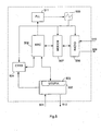
- Figure 8 and 9 show the structure of the counter block 405 for the indoor control units 4 and 8.
- Figure 8 shows the counter block structure for ATM155 systems.
- a clock 701 which is the E1 clock at 2.048 MHz is fed to a 32-bit counter 702.
- the 19.44 MHz SONET clock 703 is fed to a 32-bit counter 704 whose 32 outputs are fed to the D inputs of a 32-bit latch 705.
- the outputs of the counter 704 are latched into the 32-bit latch 705 by the E1 clock 701.
- the outputs of the counters 702 and 705 are fed to outputs 706 and 707 as outputs Q3 and Q4 respectively.
- Figure 9 shows the structure of the counter block for ATM25 services.
- the counter structure is identical to that of Figure 8 , but the clock 701 is an 8 KHz clock while the clock 703 is an E1 clock at 2.048 MHz.
- the counter structures in the indoor control units as shown in Figures 8 and 9 and the outdoor units as shown in Figures 6 and 7 are basically similar. The only significant difference is the presence of the divider 602 in the outdoor units. It will also be noticed that the slower clock latches the faster clock counter into the 16-bit or 32-bit latch. This means that a transition of the lower frequency clock is used to latch the higher frequency clock count. In this way it is possible to measure phase to an accuracy of one period of the higher frequency clock.
- the counter outputs Q1 and Q2 which are read by the media access controller 508 are the current 8 KHz clock count and a snap shot of the 40 MHz counter taken at a rising edge of the 8 KHz clock.
- the 8 KHz counter wraps approximately every eight seconds and the 40 MHz counter wraps every 1.6 milliseconds. Given that the readings are sent every second to the indoor control unit 8 at the customer premises equipment, the indoor control unit at the customer premises unit uses the output Q1 to unwrap Q2 which will have wrapped 610 or 611 times between readings.
- the outdoor unit is an ATM25 outdoor unit the 8 KHz clock is also inserted into the ATM25 data stream as the timing reference so that the same clock will be counted in the indoor control unit.
- the outdoor unit is an ATM155 outdoor unit the 19.44 MHz clock is the one used to drive the SONET physical interface and hence the same clock is counted in the indoor control unit.
- the sequence of events is as follows.
- the base station indoor control unit 5 uses the local E1 clock to time fixed intervals, for example one second intervals. At each interval it reads the local indoor control unit count values Q3 and Q4 and also the outdoor unit count values Q1 and Q2 via the link 6. All four values are assembled into an ATM cell along with a sequence number identifying the particular ATM cell, ie the sequence number increments with each successive ATM cell. The cell is then broadcast to the indoor control units of all customer premises equipment 3.
- each customer premises equipment indoor control unit 8 reads the outputs of Q3 and Q4 of its local indoor control unit counters 405 and also the outputs Q1 and Q2 of its local outdoor unit counters 504.
- a local sequence number based on the rate of change of the local indoor control unit E1 count is also generated. All ten count values are then sent to the wander evaluation process carried out in the microprocessor 404.
- Figure 10 shows a high level flow diagram for the wander evaluation process.
- 64-bit cumulative counters are kept for all ten count values (Q1 to Q4 and a sequence number from the base station 1 and corresponding values from the customer premises equipment 3). If there is a significant outage over the air then the unwrapping process fails and a wander estimate cannot be made until two consecutive new count sets arrive to reset the unwrapping process. If any of the 64-bit cumulative counters are close to wrapping then this is handled in a controlled manner and they are all reset (to non-zero values).
- the process starts, step 801, by resetting all cumulative counters.
- the next step 802 is the detection of a new ATM cell containing count values arriving from the base station.
- Step 803 of the process is to collect the local indoor control unit and outdoor unit counter values, that is, Q1 to Q4 and the sequence number.
- the base station indoor control unit and outdoor unit count values and sequence number are in the ATM cell which has arrived.
- the next step 804, is to unwrap all the count values and to update the cumulative counters.
- a decision 805, is then taken as to whether the unwrapping failed or was successful. If the unwrapping was successful, then a further decision 806, is taken as to whether the cumulative counters are near to wrapping. If the cumulative counters are not near to wrapping then the next step 807 is to calculate the change in wander using current and previous cumulative values.
- the next step 808, is to update the total wander and frequency offset.
- step 805 it was detected that the unwrapping process failed, then the process loops back to step 802 and awaits the arrival of a further ATM cell. If at step 806 it is detected that the cumulative counters are near to wrapping then a further step 809, is taken in which the cumulative counters are reset to the difference between current and previous values. Step 810 is then entered where the change in wander using the current and cumulative values and zeros is undertaken. Subsequently, the total wander and frequency offset is updated in step 808. Once the total wander and frequency offset has been updated an output is calculated, step 811, and the output value is applied to a control circuit in the indoor control unit to lock the clock 411 to the data clock of the applied to the input of the base station.
- Step 804 unwraps counter values.
- Unwrapping requires a knowledge of the previous value so the algorithm is always working on the latest set of count values and the previous set. At the start the previous set of count values is considered to be all zeros.
- Set out below is pseudo code for the basic unwrapping function which gives the latest and previous value of a wrapping counter together with cumulative unwrapped values and will appropriately increment the cumulative value even if the counter has wrapped.
- the following function takes the full count set from either the base station or the customer premises equipment and unwraps all the counters returning incremented cumulative count values. Its inputs are the latest full set of count values, their previous values and the running cumulative totals. The function uses the sequence number to check that it can still unwrap the counters and will flag if it has been unsuccessful. The pseudo code illustrating how this function is achieved is set out below.
- the 32 bit counters in the indoor control units and the 16 bit counters in the outdoor units will wrap very frequently.
- the cumulative counters are much larger and may typically only wrap after several thousand years. In that case, it is not worth going through the exercise of detecting and trapping then wrapping. However, if smaller counters were used then detection of wrapping would be more important.
- the wander calculation algorithm used in steps 807 and 810 takes the latest cumulative count set and the previous count set and calculates the incremental wander and the instantaneous frequency offset in Hertz between the two counters, that is the clock of the input data to the source module of the Network to the clock of the output data from the terminating module of the Network.
- the following pseudo code illustrates one possible embodiment of a method by which the calculation of the incremental wander and frequency offset can be achieved.
- Figure 2 shows a Network architecture where a base station 1 is transmitting over a radio frequency link 2 to customer premises equipment 3.
- the protocols used are from SONET/SDH (Synchronous Digital Hierarchy) to ITU-T G703E1.
- the indoor control unit at a base station may in fact be a standard Pentium personal computer and have no ability to count the 19.44 MHz SONET clock. There is also no E1 clock to count at the base station.
- the SONET data is fed to input 21 and from there is connected to a multiplexer 22.
- the multiplexer 22 takes the incoming 19.44 MHz clock and uses it as the SONET clock to the indoor control unit 4 and the outdoor unit 5.
- the indoor control unit counts the 19.44 MHz clock ticks and derives one second intervals from it.
- the indoor control unit reads its counters and the counters in the outdoor unit 5 and assembles and transmits an ATM cell containing the counts. This data is sent to all the customer premises equipment indoor control units which will use the method as described with reference to Figure 10 to measure E1 wander and frequency off set.
- One advantage of this arrangement is that the customer premises equipment indoor control unit 8 does not need to know the synchronisation source at the base station.
- FIG 11 shows in block schematic form a multiplexer suitable for use as the multiplexer 22 in Figure 2 . Only those features of the multiplexer which are relevant to the present invention have been shown in Figure 11 .
- the multiplexer comprises a plurality of interface circuits 1101-1 to 1101-n. These interface circuits may be implemented as an integrated circuit produced by PMC Sierra under the type reference PM5350. This circuit is designed to interface to a synchronous optical network (SONET).
- SONET synchronous optical network
- a 19.44 MHz crystal oscillator 1103 is connected to inputs 1104-1 to 1104-n of the interface circuits 1101-1 to 1101-n.
- An input 1105 which corresponds to the input 21 in Figure 2 , receives SONET data and the SONET reference clock.
- the interface circuit 1102-1 to 1102-n switches to the clock received on the input 1105.
- the interface circuit 1101-1 is then locked to the SONET reference input.
- the interface circuit 1101-1 produces a clock output locked to the received SONET clock at output 1106-1. This output is fed to inputs 1106-2 to 1106-n of the other interface circuits which now use this clock as their reference instead of the crystal oscillator 1103. Outputs 1107-2 to 1107-n are then phase locked to the SONET reference clock received on input 1105.
- the SONET reference clock applied to input 21 in the system shown in Figure 2 will be transmitted to the indoor control unit 4 and the outdoor unit 5 via the interface circuits 1102-2 to 1102-n. These outputs are phase locked to the SONET input reference at input 21.
- the multiplexer requires a minimum of three interface circuits. If more outputs are required, then correspondingly more interface circuits have to be provided.
- Figure 3 shows the Network architecture where a SONET input data signal at input 31 to base station 1 is to be transmitted to a SONET output 33 at customer premises equipment 3.
- the input 31 is connected to a multiplexer 32 and as with the arrangement of Figure 2 , the SONET 19.44 MHz clock is relayed from the multiplexer 32 to the indoor control unit 4 and outdoor unit 5.
- the indoor control unit 4 generates a fictional E1 clock from the 19.44 MHz SONET clock and also determines one second intervals.
- ATM cells are then transmitted containing the counts in the indoor control unit 4 and outdoor unit 5.
- the 19.44 MHz clock at the customer premises equipment is located within a multiplexer 34 and the indoor control unit 8 again generates an E1 clock from the 19.44 MHZ clock produced in the multiplexer 34.
- both indoor control units create a fictional E1 count value from their local 19.44 MHz clock.
- E1 wander can still be calculated even though there are no E1 clocks present within the Network.
- the customer premises indoor control unit 8 calculates the E1 wander from the fictional E1 counts and the other counter counts and controls remotely via signalling embedded ATM cells a voltage controlled oscillator within the multiplexer 34 to reduce the E1 wander to within the limits set in the specification. This ensures that the SONET clock's wander is within ITU-T G703 specifications.
- Figure 12 shows an embediment of a multiplexer suitable for use as the multiplexer 34 in the system of Figure 3 .
- the multiplexer comprises a plurality of interface circuits 1201-1 to 1201-n. These interface circuits may be implemented as integrated circuits produced by PMC Sierra under the type reference PM5350. These circuits have an asynchronous UTOPIA interface 1202-1 to 1202-n respectively.
- a voltage controlled crystal oscillator 1203 generates a frequency of 19.44 MHz and applies this frequency to inputs 1204-1 to 1204-n of the interface circuits respectively.
- Data from, for example, the indoor control unit 8 shown in Figure 3 is received on an input 1205 and passed via the UTOPIA interface 1202-1 to a control circuit 1206 which controls the frequency of the voltage controlled oscillator 1203.
- the indoor control unit 8 produces the correction required for the frequency of the voltage controlled oscillator 1203 from the phase differences received from the indoor control unit and outdoor unit of the base station and its own outdoor unit and indoor control unit.
- the master clock reference is the voltage controlled oscillator 1203 and determines the data reference clock on line 1207 which is connected to output 33 in the system of Figure 3 .
- the master clock for this multiplexer is the voltage controlled oscillator 1203 and it receives data via the interface circuit 1202-1 to control the control circuit 1206 which locks the voltage controlled oscillator 1203 to the reference clock applied to input 31 in Figure 3 .
- the output 1208 is the output fed to the outdoor unit 7 in the system of Figure 3 .
- Figure 13 shows a synchronisation architecture in which an E1 reference is available at the base station and all consumer premises equipments are locked to the E1 reference at the base station.
- the base station 1300 has an input 1301 to which the E1 reference clock is applied. This is applied to the indoor control unit 1302.
- the base station has a number of outdoor units two of which are shown as 1304-1, 1304-2. The actual number is dependent on system choices and may be greater than two.
- the base station also has a base station controller 1305 which controls the multiplexer 1303 so that the data to be transmitted is directed to the appropriate one of the outdoor units 1304.
- the multiplexer may also allow an ATM155 input from other sources to be fed to the outdoor units 1304.
- Each customer premises equipment 1310 comprises an outdoor unit 1311 and an indoor control unit 1312.
- the indoor control units produce an output locked to the E1 reference at output 1313.
- this architecture which is basically the same as that described with reference to Figure 1 , all the customer premises equipment are locked to the E1 reference applied to input 1301 in all sectors from the base station.
- a base station in fixed wireless access systems it is possible for a base station to transmit to various geographical sectors from a single aerial installation, that is a number of directional aerials are provided on a single post or in a single array which cover different geographical sectors.
- single array it is meant that the outdoor units may be remote from each other but each is connected to the indoor control unit 1302 and base station controller 1305 through the multiplexer 1303. Using this particular architecture, all the customer premises equipment on all sectors are phase locked to the reference E1.
- Figure 14 shows an architecture where the reference clock is ATM155 SONET reference at the base station. Customer premises equipment on all sectors are phase locked to the reference. This is essentially similar to the architecture shown in Figure 2 , but is extended to show multiple base station sectors and multiple customer premises equipments.
- the 19.44 MHz SONET reference is applied from an input 1401 in the base station 1400 to a multiplexer 1402.
- An indoor control unit 1403 is connected to the multiplexer as are two outdoor units 1404-1 and 1404-2.
- the number of outdoor units of the base station 1400 is dependent on the base station architecture and is not restricted to two.
- the 19.44 MHz SONET clock applied to the input 1401 is the master clock and the outputs from the multiplexer 1402 are locked to it.
- the indoor control unit 1403 generates a virtual E1 clock from the SONET clock and assembles the ATM cells in the same manner as described with reference to Figure 2 .
- a number of customer premises equipments 1410-1, 1410-2, only two of which are shown, are provided and receive over a radio link data from the base station 1400.
- Each customer premises equipment comprises an outdoor unit 1411 and a indoor control unit 1412.
- the output of the indoor control unit in each customer premises equipment is E1 data locked to the SONET reference clock in the same manner as described with reference to Figure 2 .
- the architecture illustrated in Figure 14 is for a SONET to E1 data communication.
- the architecture shown in Figure 15 has the reference clock as an ATM SONET reference applied to input 1501 at the base station 1500 and the customer premises equipment 1510 on one or more sectors having a SONET output 1511 which is phase locked to the reference at input 1501.
- This architecture is essentially the same as that shown in Figure 3 but is expanded to enable a base station with a plurality of sectors to have the customer premises equipment on all sectors phase locked to the reference at input 1501.
- a multiplexer 1513 is required having a voltage controlled 19.44 MHz crystal oscillator reference to allow the multiplexer to adjust its clock to be phase locked to the reference at input 1501.
- the multiplexer 1502 at the base station merely has to propagate the reference clock from the input 1501 to the outdoor unit 1504-1, 1504-2 and to the indoor control unit 1503 to enable the indoor control unit 1503 to produce the virtual E1 clock and assemble the ATM cells to transmit the count values.
- the multiplexer 1502 will take the form shown in Figure 11 while the multiplexer 1513 will take the form shown in Figure 12 .
- the base station controller merely has to broadcast timing count values from the reference customer premises equipment as if they were its own.
- the fact that the radios of the outdoor units at all customer premises equipment are locked to the same 40 MHz reference means that this substitution will be valid.
- the 40 MHz reference is the radio link reference and all the customer premises equipment are phase locked to the base station.
- the reference clock is the SONET input at one customer premises equipment and customer premises equipment on that sector only are phase locked to the reference.
- Customer premises equipment 1600 is the originating module on the network and receives an input at input 1601 which is a SONET reference, that is the 19.44 MHz clock reference for the Network.
- the input 1601 is fed to a multiplexer 1602.
- An indoor control unit 1603 and an outdoor unit 1604 are connected to the multiplexer. This is essentially the same as the base station 1 in the architecture of Figure 2 and operates in the same manner.
- the appropriate counter information is sent to the base station 1610 from which it is rebroadcast to a further customer premises equipment 1620.
- the customer premises equipment 1620 comprises an outdoor unit 1621 and an indoor control unit 1622 having an output 1623 which is an E1 output phase locked to the SONET reference 1601. This is accomplished in essentially the same manner as described with reference to Figure 2 but with the interposition of a base station in the radio link 2.
- the architecture is possible since all customer premises equipment 40 MHz radio clocks are locked to the base station 40 MHz clock.
- FIG 17 shows the situation where the reference clock is an E1 reference applied at an input 1701 to a customer premises equipment 1700.
- a base station 1710 communicates with the customer premises equipment and receives data transmitted from the customer premises equipment 1700.
- the base station also relays data from the customer premises equipment 1700 to a further customer premises equipment 1720.
- the customer premises equipment 1700 comprises an indoor control unit 1702 and an outdoor unit 1703.
- the customer premises equipment 1720 comprises an indoor control unit 1721 and an outdoor control unit 1722.
- the indoor control unit 1721 produces an output 1723 which is locked to the E1 reference applied to the input 1701 of the customer premises equipment 1700. This is accomplished in essentially the same manner as described with reference to Figure 1 but with the interposition of a base station in the radio link 2.
- Figure 18 illustrates the situation where there is a SONET synchronisation reference at an input 1801 to a customer premises equipment 1800 and further customer premises equipments have SONET outputs phase locked to the SONET input.
- a base station 1810 receives data from the customer premises equipment 1800 and retransmits to a further customer premises equipment 1820 on the same sector. That is, the retransmission takes place using the same outdoor unit in the base station as that which receives the data from the customer premises equipment 1800
- the customer premises equipment 1800 comprises an indoor control unit 1802, a multiplexer 1803 and an outdoor unit 1804.
- the customer premises equipment 1820 comprises an outdoor unit 1821, a multiplexer 1822 and an indoor control unit 1823.
- the multiplexer 1822 includes a voltage controlled oscillator to produce a frequency locked 19.44 MHz SONET clock.
- the data output from the customer premises equipment 1820 is available at an output 1824 derived from the multiplexer 1822.
- This architecture is essentially the same as that shown and described with reference to Figure 3 . Again the base station 1810 merely provides a relay in the radio path between the multiple customer premises equipments and the fact that the radios at all the customer premises equipments are locked to the same 40 MHz reference means that the timing count values from the reference customer premises equipment are broadcast by the base station as though they were its own.
- Figures 19 , 20 and 21 illustrate various architectures where a multiple sector base station is in self backhaul mode. That is a customer premises equipment either within that sector or on a dedicated point-to-point link is the Network interface and therefore synchronisation reference. There are three variants on this theme.
- the first architecture illustrated in Figure 19 is where an E1 synchronisation reference is provided at the backhaul customer premises equipment and an E1 output is provided at further customer premises equipment.
- a backhaul customer premises equipment 1900 has an E1 reference input 1901 connected to its indoor control unit 1902.
- the indoor control unit 1902 is connected via a fibre optic link 1903 to an outdoor unit 1904.
- the outdoor unit 1904 transmits over a radio link 1905 to a base station 1910.
- the base station 1910 comprises an indoor unit 1911, a multiplexer 1912, a first outdoor unit 1913-1 and a second outdoor unit 1913-2.
- the base station transmits to a further customer premises equipment 1920 over a radio link 1915.
- the customer premises unit equipment 1920 comprises an indoor control unit 1921, and an outdoor unit 1922.
- E1 data locked to the reference at the input 1901 of customer premises equipment 1900 is available at output 1923 of customer premises equipment 1920.
- the first method is to pull the 19.44 MHz reference at the multiplexer 1912 in the base station to phase lock it to the E1 reference at the customer premises equipment 1900.
- Each sector then uses the multiplexer's 19.44 MHz clock as a local reference. That is the base station indoor unit 1911 can do the same calculations to determine the wander using counters in the indoor control unit 1902, the outdoor unit 1904, the outdoor unit 1913-1, and the indoor control unit 1911.
- a phase locked loop within the multiplexer 1912 then pulls the 19.44 MHz oscillator to lock it to the E1 reference.
- the customer premises equipment 1920 uses the 19.44 MHz clock of the multiplexer 1912 as the local reference.
- the second method is for the multiplexer 1912 to present the same floating 19.44 MHz clock to all the outdoor units of the base station and an extra set of counters are used to measure the frequency difference between each outdoor unit's 40 MHz clock and the backhaul outdoor unit's 40 MHz clock using the 19.44 MHz of the multiplexer 1912 as a common reference.
- the hardware method with a phase locked multiplexer clock in the base station will scale more simply for multiple backhaul hops as the indoor control unit of the base station will not need to know the full backhaul topology.
- the software method requires the base station indoor control unit to have an exact knowledge of all backhaul hops and access to counters in all of the backhaul hop outdoor units.
- Figure 20 shows the architecture where the synchronisation source is a SONET reference at an input 2001 of customer premises equipment 2000 and the data out is E1 at an output 2023 of a further customer premises equipment 2020 locked to the SONET reference at input 2001.
- the customer premises equipment 2000 comprises an indoor control unit 2002, a multiplexer 2003 and an outdoor unit 2004.
- the base station comprises an indoor control unit 2011, a multiplexer 2012, and two outdoor units 2013-1 and 2013-2.
- the customer premises equipment 2020 comprises an indoor control unit 2021 and an outdoor unit 2022.
- the system shown in Figure 20 operates in substantially the same way as the architecture described with reference to Figure 2 but using either of the two methods described with reference to Figure 19 to lock the multiplexer 2012 in the base station 2010 to the SONET reference or to float the clock in the multiplexer 2012 and use an extra set of counters to measure the frequency difference between each outdoor unit's 40 MHz clock.
- the reference clock at the source customer premises equipment is SONET and the destination customer premises equipment on all sectors are phase locked to that reference.
- FIG 21 shows the situation where a SONET reference at a backhaul or source customer premises equipment is provided and a SONET output at a destination customer premises equipment on another sector is produced.
- a SONET reference is applied to an input 2101 of a customer premises equipment 2100 and to a multiplexer 2102 therein.
- an E1 reference clock is generated in indoor control unit 2103 to enable the counter counts to be assembled into ATM packets and transmitted from the outdoor unit 2104 over the radio link 2105 to the base station 2110.
- the base station 2110 comprises an indoor control unit 2111, a multiplexer 2112 and two outdoor units 2113-1 and 2113-2.
- the customer premises equipment 2120 comprises an indoor control unit 2121, an outdoor unit 2122 and a multiplexer 2123 which has a voltage controlled oscillator in similar manner to the multiplexer 34 in Figure 3 . Again, there are the same two methods for synchronising the source and destination SONET clocks as described with reference to the architectures of Figures 19 and 20 .
- Figure 22 illustrates the software method of synchronising an E1 or SONET reference at the input to a backhaul customer premises equipment with an E1 output at a customer premises equipment on another sector.
- the backhaul customer premises equipment 2200 has an input 2201 to which a SONET reference is applied.
- the customer premises equipment comprises an indoor control unit 2202, a multiplexer 2203 and an outdoor unit 2204.
- the customer premises equipment 2200 transmits data over a radio link 2205 to a base station 2210.
- the base station comprises an indoor control unit 2211, a multiplexer 2212, a first outdoor unit 2213-1 and a second outdoor unit 2213-2.
- the base station transmits data from outdoor unit 2213-2 over a radio link 2215 to a customer premises equipment 2220.
- the customer premises equipment comprises an indoor unit 2221 and an outdoor unit 2222.
- the indoor unit has an output 2223 at which E1 data is made available which is locked to the SONET input at input 2201 of customer premises equipment 2200.
- the base station controller must broadcast on each sector the content of the counters Q1, Q2, Q3 and Q4 from the backhaul customer premises equipment 2200. It must also broadcast the counters Q1 and Q2 from the outdoor unit 2213-1 which receives the data from the backhaul customer premises equipment. It must then transmit from each outdoor unit in each sector the Q1 and Q2 counts.
- the customer premises equipment 2220 can then substitute frequency C2 1 for C2, that is the 40 MHz radio clock from outdoor unit 2213-1 and the 40 MHz radio link clock from the outdoor unit 2213-2 using the backhaul outdoor unit 2213-1 counters Q1 and Q2 and the counters Q1 and Q2 in the transmitting outdoor unit 2213-2.
- This gives ⁇ SU_Q ⁇ 2 ⁇ ⁇ ⁇ SU_Q ⁇ 2.
- FIG. 23a shows two clocks. Initially the dotted clock is faster than the solid clock and then after 15 time units the dotted clock slows down. Over the total period (30 time units) both clocks have gone through the same number of cycles ie the total wander over the period shown is zero.
- phase difference between waveforms is often zero, as phase is a modulo function, ie it wraps every 360 degrees and hence has no 'memory' of accumulated cycles.
- Figure 23b shows wander. It can be seen that wander is only zero at two points, the start and finish. At the worst point, after 15 time units, the wander is approximately 1.2 cycles. If the wander were allowed to continue it would cause buffer overflows or under-runs in communication equipment and synchronisation would be lost.
- the present invention tracks wander which means that even if the system is not phase locked at any one point in time, the method tracks the accumulated wander and allows the system to recover the lost or gained cycles by speeding up or slowing down clocks.
- the method described herein actually tracks wander rather than instantaneous phase and hence is better suited than a method which merely tracks instantaneous phase.
Landscapes
- Engineering & Computer Science (AREA)
- Computer Networks & Wireless Communication (AREA)
- Signal Processing (AREA)
- Multimedia (AREA)
- Computer Hardware Design (AREA)
- Data Exchanges In Wide-Area Networks (AREA)
- Synchronisation In Digital Transmission Systems (AREA)
Description
- The invention relates to a packet switched communications system and to a method of recovering clock signals in such a system.
- Asynchronous Transfer Mode (ATM) is a packet based transport medium designed to be able to carry a wide range of traffic types simultaneously. Communications Networks and in particular fixed wireless access systems (FWA) may use ATM as their inter module transport medium and over the air transport medium. Desirably such systems should be arranged to be flexible and able to be deployed in a wide range of configurations with varying topology. In order to minimise cost, the ATM Physical Interface type may be ATM UNI (User Network Interface), which converts ATM155 SONET synchronous fibre optic interfaces into wired UTOPIA asynchronous interfaces. One disadvantage of this design choice, is the loss of physical layer synchronisation between each module. This means that end-to-end there is no synchronisation over the network.
- In a typical simple FWA system, data flowing between the base station (AP) and customer premises equipment (SU) would be carried over three unsynchronised separate links: the base station multiplexer (AP-Mux) to the base station outdoor unit (AP-ODU) via ATM155, the AP-ODU to the customer premises equipment outdoor unit (SU-ODU) via a radio link, and the SU-ODU to the customer premises indoor control unit (SU-ICU) via ATM155 or ATM25. Each link eg AP-Mux to AP-ODU has a common frequency reference for that link ie the physical layer symbol rate, but this clock floats ie there is no ability to lock it to another reference. So across any one network node, the data is transferred from one physical layer to another.
- One of the desirable types services for a Fixed Wireless Access system to support are plesiochronous digital hierarchy (PDH) services, specifically ITU-T G703 E1.
- This is a synchronous service which requires network synchronisation to international standards, e.g. ITU-T G.823. In order to achieve this two solutions have been proposed. The first is to make a common clock reference available to all interface points in the network where the E1 is sourced or sunk. The second is for the transport network to carry synchronisation information with the data and regenerate an output clock traceable back to a network timing reference. The first solution requires high tolerance clocks available throughout the network and is expensive. The second solution is the only cost effective solution for a Fixed Wireless Access Network.
- Typically a FWA system will lock all the physical layer clocks to the synchronisation source, ie each node recovers the clock from the input link and uses this to lock a Phased Locked Loop which drives the output link. In this way all clocks within the system are phase locked. This is, however, both expensive in terms of additional circuitry and also prone to cause radio link problems if the reference clock is particularly noisy.
-
EP 0718995 discloses a system which allows synchronisation of a clock signal of a first data terminal to a second data terminal connected to one another via a network. The network includes a network reference clock. - The invention provides a packet switched communications system for transmitting synchronous data from a source module to a terminating module over a network, the network comprising plurality of modules interconnected via transmission links, characterised by each module having a data clock of nominal frequency that is independent of the clocks of the other module(s) in the network and having a single input and one or more outputs, where all the outputs of each module are phase locked to each other but are unsynchronised with respect to the input, means for determining an accumulated phase difference between an input data clock and an output data clock of each module, means for transmitting the accumulated phase difference to the terminating module in the network, and means for utilising the received accumulated phase difference at a terminating module to lock the output data clock at the terminating module to an input data clock at the source module.
- In a system according to the invention the relative drift of each link with respect to its neighbours is tracked, rather than attempting to synchronise each ATM link, and the final output data clock, which is to be locked to the input data clock, is corrected using the tracked relative drift.
- The determining means may comprise a first counter for counting clock cycles of the input data clock, a second counter for counting cycles of the output data clock, and means for simultaneously reading the counts of the first and second counters.
- This has the advantage with respect to using true analogue phase detectors of being able to keep track of accumulated phase differences over time. Conventional analogue phase detectors only indicate instantaneous phase difference and give no information on accumulated phase differences or wander (ie accumulated phase difference). A disadvantage of using counters is that the phase resolution is only available in terms of integer cycles of the counters.
- The system may comprise a latch for storing the count of the counter counting the higher frequency data clock, the count being clocked into the latch by an edge of the lower frequency data clock.
- By clocking the count of the higher frequency clock into the latch on a transition of the lower frequency clock the timing resolution is that of the higher frequency clock. For example in a system with an ATM SONET and E1 link the available clocks are 19.44 MHz and 2.048 MHz, respectively. By clocking the 19.44 MHz counter into the latch on a transition of the 2.048 MHz clock phase can be measured to a precision of one 19.44 MHz period, or 51.4 nS, rather than one 2.048 MHz period, or 488 nS.
- If an analogue phase detector is used in addition to the counters a more accurate measure of the accumulated phase difference may be obtained, the counters being used to determine how many times the analogue phase detector has wrapped and the analogue phase detector giving the instantaneous phase difference.
- The invention further provides a method of recovering clock signals in a packet switched communications network, the network comprising a plurality of modules interconnected via transmission links, characterised by each module having a data clock of nominal frequency but that is independent of the data clocks of the other module(s) and each module having a single input and one or more outputs where all the outputs of each module are phase locked to each other but are unsynchronised with respect to the input, the method comprising the steps of:
- a) determining an accumulated phase difference between an input data clock and an output data clock at each module,
- b) transmitting the determined accumulated phase difference to a terminating module, and
- c) utilising the received accumulated phase difference at the terminating module to recover the data clock at a source module of the network.
- The method is based on the appreciation that it is not necessary to phase lock the input and output clocks at each module (or node) in the Network but that if the accumulated phase difference is measured at each module and transmitted to the terminating module then it is possible to lock the output clock at the terminating module to the input clock at the source module using the measured and transmitted accumulated phase differences between the input and output clocks at each module.
- The above and other features and advantages of the invention will be apparent from the following description, by way of example, of embodiments of the invention with reference to the accompanying drawings, in which:
-
Figure 1 shows in block schematic form a first embodiment of a communications Network according to the invention, -
Figure 2 shows in block schematic form a second embodiment of a communications Network according to the invention, -
Figure 3 shows in block schematic form a third embodiment of a communications Network according to the invention, -
Figure 4 shows in block schematic form an embodiment of an indoor control unit for a base station and a customer premises equipment, -
Figure 5 shows in block schematic form an embodiment of an outdoor unit for a base station and a customer premises equipment, -
Figure 6 shows the counter structure in the outdoor units of a base station and a customer premises equipment for ATM155 transport medium, -
Figure 7 shows the counter structure in the outdoor units of a base station and a customer premises equipment for ATM25 transport medium, -
Figures 8 shows the counter structure in the indoor control unit of a base station and a customer premises equipment, for ATM155 transport medium, -
Figure 9 shows the counter structure in the indoor control unit of a base station and a customer premises equipment for ATM25 transport medium, -
Figure 10 is a flow diagram illustrating the process used to convert the counter values to a phase difference, -
Figure 11 shows in block schematic form a first embodiment of a multiplexer for use in a system according to the invention, -
Figure 12 shows in block schematic form a second embodiment of a multiplexer for use in a system according to the invention, -
Figure 13 shows in block schematic form a fourth embodiment of a communications Network according to the invention, -
Figure 14 shows in block schematic form a fifth embodiment of a communications Network according to the invention, -
Figure 15 shows in block schematic form a sixth embodiment of a communications Network according to the invention, -
Figure 16 shows in block schematic form a seventh embodiment of a communications Network according to the invention, -
Figure 17 shows in block schematic form an eighth embodiment of a communications Network according to the invention, -
Figure 18 shows in block schematic form a ninth embodiment of a communications Network according to the invention, -
Figure 19 shows in block schematic form a tenth embodiment of a communications Network according to the invention, -
Figure 20 shows in block schematic form an eleventh embodiment of a communications Network according to the invention, -
Figure 21 shows in block schematic form a twelfth embodiment of a communications Network according to the invention, -
Figure 22 shows in block schematic form a thirteenth embodiment of a communications Network according to the invention, and -
Figure 23 illustrates instantaneous and accumulated phase differences between two clock signals. -
Figure 1 shows in block schematic form a first embodiment of a communications system according to the invention. As shown inFigure 1 the communications systems comprises a Network having abase station 1 which communicates via aradio link 2 with a plurality of customer premises equipment, one of which is shown as 3. Thebase station 1 comprises anindoor control unit 4 and anoutdoor unit 5. Theindoor control unit 4 communicates with theoutdoor unit 5 over afibre optic link 6. The customer premises equipment comprises anoutdoor unit 7 and anindoor control unit 8 which are coupled by afibre optic link 9. The clock frequency of the data communicated between theindoor control unit 4 and theoutdoor unit 5 of the base station will be approximately 155.52 MHz locked to a 19.44 MHz clock. The clock frequency between theoutdoor control unit 5 of the base station and theoutdoor unit 7 of the customer premises equipment will be approximately 3.5 GHz locked to a 40 MHz clock. The clock frequency of the data transmitted between theoutdoor unit 7 of the customer premises equipment and theindoor control unit 8 will be approximately 155.52 MHz locked to a 19.44 MHz clock when ATM155 is the mode of transmission or approximately 32 KHz when ATM25 is used as the transport medium. In the case of ATM25, however, the data rate is only 25 Mbits/s and the reference clock transmitted is 8 KHz derived from a 32 MHz clock by division. The frequencies mentioned above are examples only and are determined by the particular embodiments of base station and customer premises equipment and by the transmission standards and protocols used. The invention is not limited to the examples given and may be applied to networks having different topologies and using different transmission standards and protocols. - All three clocks are independent of each other that is they float relative to one another. Each will be derived from a separate crystal oscillator. The crystal oscillators are preferably not of great precision, that is, not oven controlled crystal oscillators due to cost considerations and as a result the frequency of each of the oscillators will vary with temperature, aging of the crystals, etc.
-
Figure 1 illustrates an embodiment in which PDH services specifically ITU-T G703E1 are to be transmitted. This is a synchronous service which requires Network synchronisation to international standards, for example, ITU-T G823. This means that the data clock atoutput 11 has to be locked to the data clock at theinput 10. In order to achieve this the accumulated phase differences between the various clocks are determined at each of themodules indoor control unit 4 sends an ATM cell every second to all the customer premises equipmentindoor control units 8. The ATM cell contains the values of the accumulated phase differences determined in theindoor control unit 4 and theoutdoor unit 5 of thebase station 1. Theindoor control unit 8 at thecustomer premises equipment 3 also obtains over thetransmission link 9 the accumulated phase difference measured in theoutdoor unit 7 and has a knowledge of the accumulated phase differences in theindoor control unit 8. From these accumulated phase differences it calculates the relative wander and frequency offset between the data clock at theinput 10 and the data clock produced by theindoor control unit 8. It then uses a control circuit to control a clock generator in theindoor control unit 8 to bring it into synchronisation with the data clock applied at theinput 10. - Thus, if each Network module is considered as a black box with one input connection and a number of output connections, where all the output connections are phase locked with respect to each other but totally unsynchronised with respect to the input connection, it is only necessary to measure the accumulated phase difference between the input clock and the output clock at each stage and pass this information to the final terminating stage in the Network. The final terminating stage can then calculate from these phase differences the correction needed to its output clock to lock the frequency of the output clock to the data clock of the input to the Network.
-
Figures 4 and5 show in block schematic form embodiments of indoor control units and outdoor units suitable for use as theindoor control units outdoor units Figure 1 . As shown inFigure 4 the indoor control unit has aninput 401 which is connected to aninterface circuit 402. Theinterface circuit 402 may be implemented as an integrated circuit available from Dallas Semiconductors under the type reference DS2148. This circuit takes an E1 data signal and extracts the data clock and also presents the data at an asynchronous interface 403. This data is read by amicroprocessor 404 which assembles the data into appropriate ATM cells for transmission. Theinterface circuit 402 has a further output which is connected to acounter block 405. The clock output produced by theinterface circuit 402 will be at a nominal frequency of 2.048 MHz and will be locked to the clock generated at the source of the data applied to theinput 401. Aclock generator 406 which generates a nominal frequency of 19.44 MHz is fed to aninterface circuit 407. This interface circuit may be implemented as an integrated circuit produced by PMC Sierra under the type reference PM5350. This circuit is designed to interface to a synchronous optical network (SONET). Theinterface circuit 407 has anasynchronous interface 408 using the UTOPIA protocol. Themicroprocessor 404 feeds the ATM cells it has generated to the UTOPIA interface for onward transmission via anoutput 409. When used in the system shown inFigure 1 , theoutput 409 is fed to theoptical fibre link 6. Theinterface circuit 407 also has a clock output which replicates the frequency of theclock generator 406. It will be appreciated that theclock generator 406 is not synchronised with the clock generator at the source of the data applied to input 401, although since it is derived from a crystal oscillator it will be of relatively high accuracy in frequency. This output is fed to thecounters 405. Thecounters 405 count the clock pulses from theseinterface circuits microprocessor 404 reads the clock counts at one second intervals. It then assembles them into an ATM cell to send across the Network. That is, in this embodiment, the method of measuring the accumulated phase difference between the clock output from theinterface unit 402 that is the E1 data clock applied to theinput 401 and theclock generator 406. Is should be appreciated that the invention is not limited to this particular means of determining accumulated phase difference. -
Figure 5 shows in block schematic form embodiments of theoutdoor units input 501 to which theoptical link 6 is connected. Theinput 501 is connected to aninterface circuit 502 which may be that designed and sold by PMC Sierra under the type reference PM5350. As with theinterface circuit 407, theinterface circuit 502 has anasynchronous data output 503 which operates according to the UTOPIA protocol. Theinterface circuit 503 also derives a clock from the data input applied to input 501 and outputs this clock to acounter array 504. Aclock generator 505, which may be a crystal oscillator operating at anominal frequency 40 MHz and which is not synchronised with the clock of thedata input 501, is fed to thecounters 504 and also to aradio module 506 and amodem 507. Amedia access controller 508 takes the ATM cells from the UTOPIA interface and applies them to themodem 507 where they are appropriately processed for application to theradio module 506 which then transmits them fromoutput 509 over theair link 2. Themedia access controller 508 also reads the counters at one second intervals and sends their counts to theindoor unit 4 for insertion into the ATM cell which transmits the accumulated phase differences to the terminating module on the Network. - The
outdoor unit 7 at thecustomer premises equipment 3 receives the data transmitted by the base station atinput 510. Theradio module 506 andmodem 507 process the received signal and themodem 507 feeds the data to themedia access controller 508. Themedia access controller 508 produces from the signal received from the modem 507 a control signal which is fed to acontrol circuit 511 to lock theclock generator 505 to theclock generator 505 of theoutdoor unit 5 of thebase station 1. That is the clock of theoutdoor unit 7 is locked to that of theoutdoor unit 5. Data received at themedia access controller 508 is fed to theUTOPIA interface 503 and via theinterface circuit 502 to thefibre optic link 9 throughoutput 512. It is assumed in this case that theSONET data link 9 is controlled from theindoor control unit 8 and in this case the 19.44 MHz clock for theinterface circuit 502 will be derived from theinput 501. Again, themedia access controller 508 will read the counter counts at one second intervals and this data will be transmitted via the UTOPIA interface to theindoor control unit 8 over thelink 9. - At the
indoor control unit 8 data is received over thelink 9 via the input 410 (Figure 4 ) and is read from the UTOPIA interface by themicroprocessor 404. Themicroprocessor 404 will receive data representing the accumulated phase differences between the various floating clock generators in the base station indoor control unit and outdoor unit sent via the ATM cells and will also receive from themedia access controller 508 the phase information from theoutdoor unit 7. A voltage controlledcrystal oscillator 411 produces a clock output at a nominal frequency of 2.048 MHz which it is desired should be phase locked to the 2.048 MHz clock of the input data signal atinput 10 in order that E1 data received atinput 10 can be reproduced atoutput 11 in a synchronous manner. The output of theVCO 411 is fed to thecounters 405, via theinterface circuit 402, together with the output of theclock 406. The microprocessor uses the outputs of these counters together with those received from themodules VCO 411 and the data clock at theinput 10. Themicroprocessor 404 then produces an appropriate signal to feed acontrol circuit 412 which pulls the output frequency of theoscillator 411 so that accumulated phase differences between it and the input clock of the data signal applied atinput 10 of thebase station 1 are reduced to a minimum value. The data transmitted from theinput 10 to be delivered at theoutput 11 is fed by themicroprocessor 404 to the data interface 403 and through theinterface circuit 402 to anoutput 413, theoutput 413 being connected to theoutput 11 of the Network. In this way E1 data can be transmitted through the Network even though the clocks in the various modules are not synchronised with one another. - In the embodiments described, counters have been used rather than true analogue phase detectors. A prime reason for this is that counters can keep track of accumulated phase over time whereas traditional analogue phase detectors only give information on the instantaneous phase difference and give no information on accumulated phase difference or wander. The disadvantage of using counters is that the phase resolution is only available in terms of integer cycles of the counters. It would be possible to use both counters and analogue phase detectors to give both instantaneous phase values with greater precision and also accumulated phase. A further alternative is to use an analogue phase detector with a counter which counts the number of times and the direction in which the analogue counter wraps to keep a note of accumulated phase differences or wander.
-
Figures 6 and 7 show the structure of thecounter block 504 for use in theoutdoor units counters 504 for ATM155 systems is shown in fromFigure 6 . The 19.44MHz clock 601 is derived from theinterface circuit 502 and is fed to adivider 602 which divides the clock by 2,430 to produce an 8 KHz output. The 40MHz clock 505 is applied to a 16-bit counter 603 whose 16-bit outputs are connected to the D inputs of a 16-bit latch 604. The 8 KHz output from thedivider 602 is fed to a 16-bit counter 605. The 8 KHz clock is also used to latch the output of the 16-bit counter 603 into the 16-bit latch 604. The counter outputs are then read fromoutputs - The structure for ATM25 transmissions shown in
Figure 7 is identical to that for ATM155 transmissions apart from the frequency of theclock 601 and division ratio of thedivider 602. In this case, theclock 601 has a frequency of 32 MHz and thedivider 602 has a division ratio of 4,000. This again produces an 8 KHz clock at the output of thedivider 602. - As is known to the person skilled in the art ATM25 links have a data rate of 25 Mb/s but are locked to a 32 MHz clock. In order to synchronise the two ends of the link an 8 KHz clock is transmitted in the 25 Mb/s data stream, the 8 KHz clock being derived by dividing the 32 MHz clock.
-
Figure 8 and 9 show the structure of thecounter block 405 for theindoor control units Figure 8 shows the counter block structure for ATM155 systems. Aclock 701 which is the E1 clock at 2.048 MHz is fed to a 32-bit counter 702. The 19.44MHz SONET clock 703 is fed to a 32-bit counter 704 whose 32 outputs are fed to the D inputs of a 32-bit latch 705. The outputs of thecounter 704 are latched into the 32-bit latch 705 by theE1 clock 701. The outputs of thecounters outputs Figure 9 shows the structure of the counter block for ATM25 services. The counter structure is identical to that ofFigure 8 , but theclock 701 is an 8 KHz clock while theclock 703 is an E1 clock at 2.048 MHz. - It will be seen that the counter structures in the indoor control units as shown in
Figures 8 and 9 and the outdoor units as shown inFigures 6 and 7 are basically similar. The only significant difference is the presence of thedivider 602 in the outdoor units. It will also be noticed that the slower clock latches the faster clock counter into the 16-bit or 32-bit latch. This means that a transition of the lower frequency clock is used to latch the higher frequency clock count. In this way it is possible to measure phase to an accuracy of one period of the higher frequency clock. The counter outputs Q1 and Q2 which are read by themedia access controller 508 are the current 8 KHz clock count and a snap shot of the 40 MHz counter taken at a rising edge of the 8 KHz clock. The 8 KHz counter wraps approximately every eight seconds and the 40 MHz counter wraps every 1.6 milliseconds. Given that the readings are sent every second to theindoor control unit 8 at the customer premises equipment, the indoor control unit at the customer premises unit uses the output Q1 to unwrap Q2 which will have wrapped 610 or 611 times between readings. When the outdoor unit is an ATM25 outdoor unit the 8 KHz clock is also inserted into the ATM25 data stream as the timing reference so that the same clock will be counted in the indoor control unit. When the outdoor unit is an ATM155 outdoor unit the 19.44 MHz clock is the one used to drive the SONET physical interface and hence the same clock is counted in the indoor control unit. - The sequence of events is as follows. The base station
indoor control unit 5 uses the local E1 clock to time fixed intervals, for example one second intervals. At each interval it reads the local indoor control unit count values Q3 and Q4 and also the outdoor unit count values Q1 and Q2 via thelink 6. All four values are assembled into an ATM cell along with a sequence number identifying the particular ATM cell, ie the sequence number increments with each successive ATM cell. The cell is then broadcast to the indoor control units of allcustomer premises equipment 3. On receipt of a new cell from the base stationindoor control unit 4 each customer premises equipmentindoor control unit 8 reads the outputs of Q3 and Q4 of its local indoor control unit counters 405 and also the outputs Q1 and Q2 of its local outdoor unit counters 504. A local sequence number based on the rate of change of the local indoor control unit E1 count is also generated. All ten count values are then sent to the wander evaluation process carried out in themicroprocessor 404. -
Figure 10 shows a high level flow diagram for the wander evaluation process. 64-bit cumulative counters are kept for all ten count values (Q1 to Q4 and a sequence number from thebase station 1 and corresponding values from the customer premises equipment 3). If there is a significant outage over the air then the unwrapping process fails and a wander estimate cannot be made until two consecutive new count sets arrive to reset the unwrapping process. If any of the 64-bit cumulative counters are close to wrapping then this is handled in a controlled manner and they are all reset (to non-zero values). The process starts,step 801, by resetting all cumulative counters. Thenext step 802 is the detection of a new ATM cell containing count values arriving from the base station. Step 803 of the process is to collect the local indoor control unit and outdoor unit counter values, that is, Q1 to Q4 and the sequence number. The base station indoor control unit and outdoor unit count values and sequence number are in the ATM cell which has arrived. Thenext step 804, is to unwrap all the count values and to update the cumulative counters. Adecision 805, is then taken as to whether the unwrapping failed or was successful. If the unwrapping was successful, then afurther decision 806, is taken as to whether the cumulative counters are near to wrapping. If the cumulative counters are not near to wrapping then thenext step 807 is to calculate the change in wander using current and previous cumulative values. Thenext step 808, is to update the total wander and frequency offset. The process then loops back to step 802 and awaits the arrival of the next ATM cell. If atstep 805 it was detected that the unwrapping process failed, then the process loops back to step 802 and awaits the arrival of a further ATM cell. If atstep 806 it is detected that the cumulative counters are near to wrapping then afurther step 809, is taken in which the cumulative counters are reset to the difference between current and previous values. Step 810 is then entered where the change in wander using the current and cumulative values and zeros is undertaken. Subsequently, the total wander and frequency offset is updated instep 808. Once the total wander and frequency offset has been updated an output is calculated,step 811, and the output value is applied to a control circuit in the indoor control unit to lock theclock 411 to the data clock of the applied to the input of the base station. - Step 804 unwraps counter values. There are ten counter values to be unwrapped. Q1, Q2, Q3, Q4, and a sequence number from the
base station 1 and Q1, Q2, Q3, Q4, and a sequence number from thecustomer premises equipment 3. Unwrapping requires a knowledge of the previous value so the algorithm is always working on the latest set of count values and the previous set. At the start the previous set of count values is considered to be all zeros. Set out below is pseudo code for the basic unwrapping function which gives the latest and previous value of a wrapping counter together with cumulative unwrapped values and will appropriately increment the cumulative value even if the counter has wrapped.
DEFINE cumulative INTEGER 64 bit
DEFINEnew_value INTEGER 32 bit
DEFINE tmp_new_value INTEGER 64 bit
DEFINEold_value INTEGER 32 bit
DEFINE limit INTEGER
unwrap (cumulative, new_value, old_value, limit)
{
     if new_value<old_value then
        {
         tmp_new_value:=new_value+limit
        }
     else
        {
         tmp_new_value:=new_value
        }
     return (cumulative + tmp_new_value-old_value)
    }
DEFINE ODU_delta8, ODU_delta40, wrap FLOAT unwrap_counters
(Q1_total, Q1_new, Q1_old, Q2_total, Q2_new, Q2_old, Q3_total, Q3_new, Q3_old, Q4_total, Q4_new, Q4_old, seq_no_total, seq_no_new, seq_no_old)
   {
    // unwrap sequence number and check gap in data
    fail := FALSE
    new_seq_no_total := unwrap(seq_no_total, seq_no_new,
    seq_no_old, s^32)
    if new_seq_no_total - seq_no_total>= 6 then
      {
       fail := TRUE
      }
    // unwrap Q1, Q3 and Q4
    new_Q3_total := unwrap(Q3_total, Q3_new, Q3_old,2^32)
    new_Q4_total := unwrap(Q4_total, Q4_new, Q4_old,2^32)
    new_Q1_total := unwrap(Q1_total, Q1_new, Q1_old,2^16),
    // now unwrap the 40MHz counter
    ODU_delta8 := new_Q1_total - Q1 total
    ODU_delta40 := Q2_new - Q2_old
    wrap := floor(ODU_delta8 *5000 / 65536)
    if ODU_delta40 < 0 then
      {
     wrap := wrap + 1
      }
   new_Q2_total := wrap * 65536 + ODU_delta40 + Q2_total
   return (fail,new_seq_no_total, new_Q1_total,
   new_Q2_total, new_Q3_total, new_Q4_total)
   }
   {
    AP_Q1_diff:new_AP_Q1 - old_AP_Q1
    AP_Q2_diff:new_AP_Q2 - old_AP_Q2
    AP_Q3_diff:new_AP_Q3 - old_AP_Q3
    AP_Q4_diff:new_AP_Q3 - old_AP_Q3
    SU_Q1_diff:new_SU_Q1 - old_SU_Q1
    SU_Q2_diff:new_SU_Q2 - old_SU_Q2
    SU_Q3_diff:new_SU_Q3 - old_SU_Q3
    SU_Q4_diff:new_SU_Q4 - old_SU_Q4
    // Calculate ppm difference between AP ATM 155 and SU
    ATM 155 / ATM 25 delay_40MHz_ticks:= SU_Q2 - diff
    AP_Q2diff
    wound_back_SU :=SU_Q1_diff. (1 - (delay_40MHz_ticks /
    SU_Q2_diff))
    ppm_diff:=(AP_Q1_diff - wound_back_SU)/wound_back_SU
    //Need a scale factor which compensates for ATM 25 at
    the CPE end if ATM25_SU then
    {
    //i.e. ATM 25 CPE
    scale:=1
    }
   else
    {
    //i.e. ATM 155 CPE
    scale:=2430
    }
    //Now calculate wander
    SUtick_SU_ODU_ICU_latency := SU_Q4_diff -
    SU_Q1_diff*scale
    SUtick_ODU_to_OCU_delay :=
    delay_40MHz_ticks*SU_Q1_diff*scale / SU_Q2_diff
    SUtick_AP_ICU_ODU_latency := (AP_Q1_diff*scale -
    AP_Q4_diff / scale) * (1 - ppm_diff)
    total_delay := SUtick_SU_ODU_ICU_latency +
    SUtick_ODU_to_ODU_delay + Sltick_AP_ICU_ODU_latency
    wind_back_SU_E1_ticks := total_delay * SU_Q3_diff /
    SU_Q4_diff
    wound_back_E1 := SU_Q3_diff - wind_back_SU_E1_ticks
    delta_wander := wound_back_E1 - AP_Q3_diff
    delta_AP_E1_ticks := AP_Q3_diff
    freq_diff_Hz := delta_wander / (delta_AP_E1_ticks /
    2048000)
    return (delta_wander, freq_Hz, delta_AP_E1_ticks,
    wind_back_SU_E1_ticks_)
   }

Claims (10)
- A packet switched communications system for transmitting synchronous data from a source module (4) to a terminating module (8) over a network, the network comprising plurality of modules (5, 7) interconnected via transmission links (2), characterised by each module in the network having a data clock of nominal frequency that is independent of the data clocks of the other modules in the network and having a single input and one or more outputs where all the outputs of each module are phase locked to each other but are unsynchronised with respect to the input, and further comprising: means (405, 504) for determining an accumulated phase difference between an input data clock and an output data clock of each module, means for transmitting the accumulated phase difference to the terminating module, and means for utilising the received accumulated phase difference at the terminating module to lock an output data clock at the terminating module to the input data clock at the source module.
- A system as claimed in Claim 1 in which the accumulated phase difference is transmitted at regular intervals in an ATM data cell.
- A system as claimed in Claim 1 or Claim 2 in which the determining means comprises a first counter for counting clock cycles of the input data clock, a second counter for counting cycles of the output data clock, and means for simultaneously reading the counts of the first and second counters.
- A system as claimed in Claim 3 comprising a latch for storing the count of the counter counting the higher frequency data clock, the count being clocked into the latch by an edge of the lower frequency data clock.
- A system as claimed in any of Claims 3 or Claim 4 in which the means for transmitting the phase difference comprises means for assembling an ATM cell containing the counts of the first and second counters
- A method of recovering clock signals in a packet switched communications network, the network comprising a plurality of modules (4, 5, 7, 8) interconnected via transmission links (2, 6, 9), characterised by each module having a data clock of nominal frequency that is independent of the data clocks of the other modules, each module having a single input and one or more outputs, wherein all the outputs of each module are phase locked to each other but are unsynchronised with the input, the method comprising the steps of:a) determining the accumulated phase difference between an input data clock and an output data clock at each module,b) transmitting the determined accumulated phase difference to a terminating module, andc) utilising the received accumulated phase difference at the terminating module to lock an output data clock at the termination module to the input data clock of the source module.
- A method as claimed in Claim 6 in which the network uses asynchronous transfer mode, ATM, and the accumulated phase difference is transmitted in an ATM cell
- A method as claimed in Claim 6 or Claim 7 in which step a) comprises the steps of:d) applying an input data clock of a module to a first counter within the module,e) applying an output data clock of the module to a second counter within the module,f) reading the counts of the first and second counters simultaneously at given intervals.
- A method as claimed in Claim 8 in which step d) comprises transmitting the counts read in step f).
- A method as claimed in Claim 8 or Claim 9 in which the counters are read on a transition of the lower frequency data clock.
Applications Claiming Priority (3)
| Application Number | Priority Date | Filing Date | Title |
|---|---|---|---|
| GB0208374 | 2002-04-11 | ||
| GB0208374A GB2387516B (en) | 2002-04-11 | 2002-04-11 | Communication system |
| PCT/GB2003/001477 WO2003088595A2 (en) | 2002-04-11 | 2003-04-03 | Synchronization in a communication system |
Publications (2)
| Publication Number | Publication Date |
|---|---|
| EP1493239A2 EP1493239A2 (en) | 2005-01-05 |
| EP1493239B1 true EP1493239B1 (en) | 2015-07-22 |
Family
ID=9934681
Family Applications (1)
| Application Number | Title | Priority Date | Filing Date |
|---|---|---|---|
| EP03720675.2A Expired - Lifetime EP1493239B1 (en) | 2002-04-11 | 2003-04-03 | Synchronization in a communication system |
Country Status (6)
| Country | Link |
|---|---|
| US (1) | US7602811B2 (en) |
| EP (1) | EP1493239B1 (en) |
| CN (1) | CN1647424B (en) |
| AU (1) | AU2003224252A1 (en) |
| GB (1) | GB2387516B (en) |
| WO (1) | WO2003088595A2 (en) |
Families Citing this family (12)
| Publication number | Priority date | Publication date | Assignee | Title |
|---|---|---|---|---|
| EP2130316B1 (en) * | 2007-03-20 | 2018-05-23 | Marvell World Trade Ltd. | Synchronous network device |
| US7974278B1 (en) | 2007-12-12 | 2011-07-05 | Integrated Device Technology, Inc. | Packet switch with configurable virtual channels |
| US7907625B1 (en) * | 2008-08-04 | 2011-03-15 | Integrated Device Technology, Inc. | Power reduction technique for buffered crossbar switch |
| US20100067531A1 (en) * | 2008-09-17 | 2010-03-18 | Motorola, Inc. | Apparatus and method for controlling independent clock domains to perform synchronous operations in an asynchronous network |
| US8250399B1 (en) * | 2009-01-08 | 2012-08-21 | Marvell International Ltd. | Method and apparatus for clock wander compensation |
| FR2949030B1 (en) * | 2009-08-04 | 2012-03-23 | Canon Kk | METHOD AND DEVICE FOR SYNCHRONIZING APPLICATIONS IN A NETWORK |
| WO2012133635A1 (en) * | 2011-03-30 | 2012-10-04 | 日本電気株式会社 | Relay device, relay method, and relay processing program |
| CN103259692A (en) * | 2012-02-15 | 2013-08-21 | 瑞典爱立信有限公司 | Loss measuring in link aggregation group |
| US8861664B2 (en) | 2012-06-15 | 2014-10-14 | Smsc Holdings S.A.R.L. | Communication system and method for synchronizing a plurality of network nodes after a network lock condition occurs |
| FR3002397A1 (en) * | 2013-02-20 | 2014-08-22 | Jacques Louis Marie Pontois | Method for allowing control in phase of chain of distant clocks inter-connected by communication network, for large networks of antennas for electronic warfare, involves propagating measurement of current phase error of phase-locked loops |
| WO2015100576A1 (en) * | 2013-12-31 | 2015-07-09 | 华为技术有限公司 | Method and apparatus for transmitting data |
| US10205586B2 (en) * | 2016-02-02 | 2019-02-12 | Marvell World Trade Ltd. | Method and apparatus for network synchronization |
Family Cites Families (27)
| Publication number | Priority date | Publication date | Assignee | Title |
|---|---|---|---|---|
| US4006952A (en) * | 1976-05-10 | 1977-02-08 | Puckett William E | Battery jump cable apparatus |
| JPH0267033A (en) * | 1988-09-01 | 1990-03-07 | Fujitsu Ltd | Network synchronizing system |
| JP2536929B2 (en) * | 1989-07-21 | 1996-09-25 | 富士通株式会社 | Phase matching circuit |
| US5140611A (en) * | 1989-09-29 | 1992-08-18 | Rockwell International Corporation | Pulse width modulated self-clocking and self-synchronizing data transmission and method for a telephonic communication network switching system |
| JPH05167551A (en) * | 1991-12-18 | 1993-07-02 | Fujitsu Ltd | Method of replacing pointer in synchronizing communication system |
| US5526383A (en) * | 1992-08-14 | 1996-06-11 | Fujitsu Limited | Network control system for controlling relative errors between network nodes |
| US5483201A (en) * | 1993-09-30 | 1996-01-09 | At&T Corp. | Synchronization circuit using a high speed digital slip counter |
| US5869968A (en) * | 1994-03-11 | 1999-02-09 | Baker Hughes Incorporated | Method and apparatus for avoiding mutual coupling between receivers in measurement while drilling |
| JPH07336784A (en) * | 1994-06-08 | 1995-12-22 | Toshiba Corp | Clock synchronization device |
| EP0718995A1 (en) * | 1994-12-20 | 1996-06-26 | International Business Machines Corporation | Apparatus and method for synchronizing clock signals for digital links in a packet switching mode |
| US5638379A (en) * | 1995-06-06 | 1997-06-10 | Symmetricom, Inc. | Encoding system for distribution of synchronization |
| JP2891149B2 (en) * | 1995-11-20 | 1999-05-17 | 日本電気株式会社 | Phase control loop method |
| US5640388A (en) * | 1995-12-21 | 1997-06-17 | Scientific-Atlanta, Inc. | Method and apparatus for removing jitter and correcting timestamps in a packet stream |
| JPH09247176A (en) * | 1996-03-11 | 1997-09-19 | Hitachi Ltd | Asynchronous transfer mode exchange system |
| DE69613703T2 (en) * | 1996-11-08 | 2002-05-16 | Alcatel Sa | Method for transparent transmission of an incoming clock signal over a network, and related circuits for receiving and transmitting |
| US6072810A (en) * | 1996-11-08 | 2000-06-06 | Alcatel | Method to transparently transport an incoming clock signal over a network segment, and related transmitter and receiver unit |
| US6222894B1 (en) * | 1996-12-18 | 2001-04-24 | Samsung Electronics Co., Ltd. | Digital delay locked loop for reducing power consumption of synchronous semiconductor memory device |
| KR100251710B1 (en) * | 1997-07-07 | 2000-04-15 | 윤종용 | Jitter and wander reduction device on the networking between atm interface and pdh interface on the ds1 line and e1 line |
| JP3433071B2 (en) * | 1997-10-29 | 2003-08-04 | 富士通株式会社 | Clock frequency synchronizer |
| US6611932B2 (en) * | 1997-12-05 | 2003-08-26 | Lightspeed Semiconductor Corporation | Method and apparatus for controlling and observing data in a logic block-based ASIC |
| JPH11214990A (en) * | 1998-01-21 | 1999-08-06 | Internatl Business Mach Corp <Ibm> | Phase lock loop |
| DE19820572A1 (en) * | 1998-05-08 | 1999-11-11 | Alcatel Sa | Desynchronisation device for synchronous digital transmission system |
| US6119016A (en) * | 1998-06-10 | 2000-09-12 | Lucent Technologies, Inc. | Synchronizing base stations in a wireless telecommunications system |
| US6791987B1 (en) * | 1998-10-23 | 2004-09-14 | Nortel Networks Limited | Maintaining synchronization over asynchronous interface |
| US6661811B1 (en) * | 1999-02-12 | 2003-12-09 | Koninklijke Philips Electronics N.V. | Method of and apparatus for communicating isochronous data |
| US6366805B1 (en) * | 1999-05-26 | 2002-04-02 | Viasys Healthcare Inc. | Time frame synchronization of medical monitoring signals |
| DE10048590B4 (en) * | 2000-09-30 | 2008-02-28 | Infineon Technologies Ag | Phase-locked loop |
-
2002
- 2002-04-11 GB GB0208374A patent/GB2387516B/en not_active Expired - Lifetime
-
2003
- 2003-04-03 CN CN03808174.1A patent/CN1647424B/en not_active Expired - Lifetime
- 2003-04-03 AU AU2003224252A patent/AU2003224252A1/en not_active Abandoned
- 2003-04-03 US US10/510,406 patent/US7602811B2/en active Active
- 2003-04-03 EP EP03720675.2A patent/EP1493239B1/en not_active Expired - Lifetime
- 2003-04-03 WO PCT/GB2003/001477 patent/WO2003088595A2/en not_active Application Discontinuation
Also Published As
| Publication number | Publication date |
|---|---|
| WO2003088595A3 (en) | 2003-12-18 |
| EP1493239A2 (en) | 2005-01-05 |
| AU2003224252A8 (en) | 2003-10-27 |
| CN1647424A (en) | 2005-07-27 |
| AU2003224252A1 (en) | 2003-10-27 |
| US7602811B2 (en) | 2009-10-13 |
| WO2003088595A2 (en) | 2003-10-23 |
| GB0208374D0 (en) | 2002-05-22 |
| GB2387516A (en) | 2003-10-15 |
| GB2387516B (en) | 2005-03-09 |
| CN1647424B (en) | 2010-08-18 |
| US20050175037A1 (en) | 2005-08-11 |
Similar Documents
| Publication | Publication Date | Title |
|---|---|---|
| US7535931B1 (en) | Two-way timing protocol | |
| EP1493239B1 (en) | Synchronization in a communication system | |
| US7043651B2 (en) | Technique for synchronizing clocks in a network | |
| KR100741213B1 (en) | Alignment of Clock Domains in Packet Networks | |
| KR100715736B1 (en) | Adaptive clock recovery | |
| US7184920B2 (en) | Delay measurement system | |
| US20020172229A1 (en) | Method and apparatus for transporting a synchronous or plesiochronous signal over a packet network | |
| CN114830593B (en) | System and method for transmitting constant bit rate client signals over a packet transmission network | |
| JPH09135226A (en) | Method and device to support tdma operation through hybrid fiber coaxial (hfc) channel or other channel | |
| CA2077288A1 (en) | Method and apparatus for transforming low bandwith telecommunications channels into a high bandwidth telecommunication channel | |
| JPS64890B2 (en) | ||
| US20050041691A1 (en) | Apparatus and methods for providing synchronous digital data transfer over an ethernet | |
| AU757626B2 (en) | Frame phase synchronous system and a method thereof | |
| AU722056B2 (en) | Virtual time loop | |
| US6198736B1 (en) | Telecommunications system | |
| US20040057539A1 (en) | Clock, data and time recovery using bit-resolved timing registers | |
| US7783200B2 (en) | Method and apparatus for constant bit rate data transmission in an optical burst switching network | |
| Li et al. | Distributed source-destination synchronization using inband clock distribution | |
| US20050025038A1 (en) | Method of and apparatus for recovering a reference clock | |
| Serizawa et al. | ATM transmissions of microprocessor-based current differential teleprotection signals | |
| JP5044361B2 (en) | Protective relay system | |
| JP2000349798A (en) | Suscriber transmitter | |
| Li et al. | Distributed source-destination synchronization | |
| Serizawa et al. | A method of constructing an SDH‐based time transfer network and its experimental examination |
Legal Events
| Date | Code | Title | Description |
|---|---|---|---|
| PUAI | Public reference made under article 153(3) epc to a published international application that has entered the european phase |
Free format text: ORIGINAL CODE: 0009012 |
|
| 17P | Request for examination filed |
Effective date: 20041101 |
|
| AK | Designated contracting states |
Kind code of ref document: A2 Designated state(s): AT BE BG CH CY CZ DE DK EE ES FI FR GB GR HU IE IT LI LU MC NL PT RO SE SI SK TR |
|
| AX | Request for extension of the european patent |
Extension state: AL LT LV MK |
|
| R17P | Request for examination filed (corrected) |
Effective date: 20041101 |
|
| RAP1 | Party data changed (applicant data changed or rights of an application transferred) |
Owner name: CAMBRIDGE BROADBAND NETWORKS LIMITED |
|
| 17Q | First examination report despatched |
Effective date: 20070710 |
|
| GRAP | Despatch of communication of intention to grant a patent |
Free format text: ORIGINAL CODE: EPIDOSNIGR1 |
|
| INTG | Intention to grant announced |
Effective date: 20150203 |
|
| GRAS | Grant fee paid |
Free format text: ORIGINAL CODE: EPIDOSNIGR3 |
|
| GRAA | (expected) grant |
Free format text: ORIGINAL CODE: 0009210 |
|
| AK | Designated contracting states |
Kind code of ref document: B1 Designated state(s): AT BE BG CH CY CZ DE DK EE ES FI FR GB GR HU IE IT LI LU MC NL PT RO SE SI SK TR |
|
| REG | Reference to a national code |
Ref country code: GB Ref legal event code: FG4D |
|
| REG | Reference to a national code |
Ref country code: CH Ref legal event code: EP |
|
| RAP2 | Party data changed (patent owner data changed or rights of a patent transferred) |
Owner name: CAMBRIDGE BROADBAND NETWORKS LIMITED |
|
| REG | Reference to a national code |
Ref country code: IE Ref legal event code: FG4D |
|
| REG | Reference to a national code |
Ref country code: AT Ref legal event code: REF Ref document number: 738405 Country of ref document: AT Kind code of ref document: T Effective date: 20150815 |
|
| REG | Reference to a national code |
Ref country code: DE Ref legal event code: R096 Ref document number: 60347839 Country of ref document: DE |
|
| REG | Reference to a national code |
Ref country code: AT Ref legal event code: MK05 Ref document number: 738405 Country of ref document: AT Kind code of ref document: T Effective date: 20150722 |
|
| REG | Reference to a national code |
Ref country code: NL Ref legal event code: MP Effective date: 20150722 |
|
| PG25 | Lapsed in a contracting state [announced via postgrant information from national office to epo] |
Ref country code: GR Free format text: LAPSE BECAUSE OF FAILURE TO SUBMIT A TRANSLATION OF THE DESCRIPTION OR TO PAY THE FEE WITHIN THE PRESCRIBED TIME-LIMIT Effective date: 20151023 Ref country code: FI Free format text: LAPSE BECAUSE OF FAILURE TO SUBMIT A TRANSLATION OF THE DESCRIPTION OR TO PAY THE FEE WITHIN THE PRESCRIBED TIME-LIMIT Effective date: 20150722 |
|
| PG25 | Lapsed in a contracting state [announced via postgrant information from national office to epo] |
Ref country code: AT Free format text: LAPSE BECAUSE OF FAILURE TO SUBMIT A TRANSLATION OF THE DESCRIPTION OR TO PAY THE FEE WITHIN THE PRESCRIBED TIME-LIMIT Effective date: 20150722 Ref country code: ES Free format text: LAPSE BECAUSE OF FAILURE TO SUBMIT A TRANSLATION OF THE DESCRIPTION OR TO PAY THE FEE WITHIN THE PRESCRIBED TIME-LIMIT Effective date: 20150722 Ref country code: PT Free format text: LAPSE BECAUSE OF FAILURE TO SUBMIT A TRANSLATION OF THE DESCRIPTION OR TO PAY THE FEE WITHIN THE PRESCRIBED TIME-LIMIT Effective date: 20151123 Ref country code: SE Free format text: LAPSE BECAUSE OF FAILURE TO SUBMIT A TRANSLATION OF THE DESCRIPTION OR TO PAY THE FEE WITHIN THE PRESCRIBED TIME-LIMIT Effective date: 20150722 |
|
| REG | Reference to a national code |
Ref country code: FR Ref legal event code: PLFP Year of fee payment: 14 |
|
| REG | Reference to a national code |
Ref country code: DE Ref legal event code: R097 Ref document number: 60347839 Country of ref document: DE |
|
| PG25 | Lapsed in a contracting state [announced via postgrant information from national office to epo] |
Ref country code: DK Free format text: LAPSE BECAUSE OF FAILURE TO SUBMIT A TRANSLATION OF THE DESCRIPTION OR TO PAY THE FEE WITHIN THE PRESCRIBED TIME-LIMIT Effective date: 20150722 Ref country code: CZ Free format text: LAPSE BECAUSE OF FAILURE TO SUBMIT A TRANSLATION OF THE DESCRIPTION OR TO PAY THE FEE WITHIN THE PRESCRIBED TIME-LIMIT Effective date: 20150722 Ref country code: IT Free format text: LAPSE BECAUSE OF FAILURE TO SUBMIT A TRANSLATION OF THE DESCRIPTION OR TO PAY THE FEE WITHIN THE PRESCRIBED TIME-LIMIT Effective date: 20150722 Ref country code: SK Free format text: LAPSE BECAUSE OF FAILURE TO SUBMIT A TRANSLATION OF THE DESCRIPTION OR TO PAY THE FEE WITHIN THE PRESCRIBED TIME-LIMIT Effective date: 20150722 Ref country code: EE Free format text: LAPSE BECAUSE OF FAILURE TO SUBMIT A TRANSLATION OF THE DESCRIPTION OR TO PAY THE FEE WITHIN THE PRESCRIBED TIME-LIMIT Effective date: 20150722 |
|
| PLBE | No opposition filed within time limit |
Free format text: ORIGINAL CODE: 0009261 |
|
| STAA | Information on the status of an ep patent application or granted ep patent |
Free format text: STATUS: NO OPPOSITION FILED WITHIN TIME LIMIT |
|
| PG25 | Lapsed in a contracting state [announced via postgrant information from national office to epo] |
Ref country code: RO Free format text: LAPSE BECAUSE OF FAILURE TO SUBMIT A TRANSLATION OF THE DESCRIPTION OR TO PAY THE FEE WITHIN THE PRESCRIBED TIME-LIMIT Effective date: 20150722 |
|
| 26N | No opposition filed |
Effective date: 20160425 |
|
| PG25 | Lapsed in a contracting state [announced via postgrant information from national office to epo] |
Ref country code: BE Free format text: LAPSE BECAUSE OF NON-PAYMENT OF DUE FEES Effective date: 20160430 Ref country code: SI Free format text: LAPSE BECAUSE OF FAILURE TO SUBMIT A TRANSLATION OF THE DESCRIPTION OR TO PAY THE FEE WITHIN THE PRESCRIBED TIME-LIMIT Effective date: 20150722 |
|
| REG | Reference to a national code |
Ref country code: CH Ref legal event code: PL |
|
| PG25 | Lapsed in a contracting state [announced via postgrant information from national office to epo] |
Ref country code: BE Free format text: LAPSE BECAUSE OF FAILURE TO SUBMIT A TRANSLATION OF THE DESCRIPTION OR TO PAY THE FEE WITHIN THE PRESCRIBED TIME-LIMIT Effective date: 20150722 Ref country code: LU Free format text: LAPSE BECAUSE OF FAILURE TO SUBMIT A TRANSLATION OF THE DESCRIPTION OR TO PAY THE FEE WITHIN THE PRESCRIBED TIME-LIMIT Effective date: 20160403 |
|
| REG | Reference to a national code |
Ref country code: IE Ref legal event code: MM4A |
|
| PG25 | Lapsed in a contracting state [announced via postgrant information from national office to epo] |
Ref country code: CH Free format text: LAPSE BECAUSE OF NON-PAYMENT OF DUE FEES Effective date: 20160430 Ref country code: LI Free format text: LAPSE BECAUSE OF NON-PAYMENT OF DUE FEES Effective date: 20160430 |
|
| REG | Reference to a national code |
Ref country code: FR Ref legal event code: PLFP Year of fee payment: 15 |
|
| PG25 | Lapsed in a contracting state [announced via postgrant information from national office to epo] |
Ref country code: IE Free format text: LAPSE BECAUSE OF NON-PAYMENT OF DUE FEES Effective date: 20160403 |
|
| PG25 | Lapsed in a contracting state [announced via postgrant information from national office to epo] |
Ref country code: NL Free format text: LAPSE BECAUSE OF FAILURE TO SUBMIT A TRANSLATION OF THE DESCRIPTION OR TO PAY THE FEE WITHIN THE PRESCRIBED TIME-LIMIT Effective date: 20150722 |
|
| REG | Reference to a national code |
Ref country code: FR Ref legal event code: PLFP Year of fee payment: 16 |
|
| PG25 | Lapsed in a contracting state [announced via postgrant information from national office to epo] |
Ref country code: CY Free format text: LAPSE BECAUSE OF FAILURE TO SUBMIT A TRANSLATION OF THE DESCRIPTION OR TO PAY THE FEE WITHIN THE PRESCRIBED TIME-LIMIT Effective date: 20150722 Ref country code: HU Free format text: LAPSE BECAUSE OF FAILURE TO SUBMIT A TRANSLATION OF THE DESCRIPTION OR TO PAY THE FEE WITHIN THE PRESCRIBED TIME-LIMIT; INVALID AB INITIO Effective date: 20030403 |
|
| PG25 | Lapsed in a contracting state [announced via postgrant information from national office to epo] |
Ref country code: TR Free format text: LAPSE BECAUSE OF FAILURE TO SUBMIT A TRANSLATION OF THE DESCRIPTION OR TO PAY THE FEE WITHIN THE PRESCRIBED TIME-LIMIT Effective date: 20150722 Ref country code: MC Free format text: LAPSE BECAUSE OF FAILURE TO SUBMIT A TRANSLATION OF THE DESCRIPTION OR TO PAY THE FEE WITHIN THE PRESCRIBED TIME-LIMIT Effective date: 20150722 |
|
| PG25 | Lapsed in a contracting state [announced via postgrant information from national office to epo] |
Ref country code: BG Free format text: LAPSE BECAUSE OF FAILURE TO SUBMIT A TRANSLATION OF THE DESCRIPTION OR TO PAY THE FEE WITHIN THE PRESCRIBED TIME-LIMIT Effective date: 20150722 |
|
| PGFP | Annual fee paid to national office [announced via postgrant information from national office to epo] |
Ref country code: FR Payment date: 20200420 Year of fee payment: 18 |
|
| REG | Reference to a national code |
Ref country code: GB Ref legal event code: 732E Free format text: REGISTERED BETWEEN 20200903 AND 20200910 |
|
| REG | Reference to a national code |
Ref country code: DE Ref legal event code: R082 Ref document number: 60347839 Country of ref document: DE Representative=s name: ANWALTSKANZLEI MEISSNER & MEISSNER, DE Ref country code: DE Ref legal event code: R081 Ref document number: 60347839 Country of ref document: DE Owner name: CAMBRIDGE BROADBAND NETWORKS GROUP LTD., GB Free format text: FORMER OWNER: CAMBRIDGE BROADBAND NETWORKS LTD., CAMBRIDGE, GB |
|
| PG25 | Lapsed in a contracting state [announced via postgrant information from national office to epo] |
Ref country code: FR Free format text: LAPSE BECAUSE OF NON-PAYMENT OF DUE FEES Effective date: 20210430 |
|
| PGFP | Annual fee paid to national office [announced via postgrant information from national office to epo] |
Ref country code: GB Payment date: 20220329 Year of fee payment: 20 |
|
| PGFP | Annual fee paid to national office [announced via postgrant information from national office to epo] |
Ref country code: DE Payment date: 20220420 Year of fee payment: 20 |
|
| REG | Reference to a national code |
Ref country code: DE Ref legal event code: R071 Ref document number: 60347839 Country of ref document: DE |
|
| REG | Reference to a national code |
Ref country code: GB Ref legal event code: PE20 Expiry date: 20230402 |
|
| PG25 | Lapsed in a contracting state [announced via postgrant information from national office to epo] |
Ref country code: GB Free format text: LAPSE BECAUSE OF EXPIRATION OF PROTECTION Effective date: 20230402 |