EP1410308B1 - Addressable ptf receptor for irradiated images - Google Patents
Addressable ptf receptor for irradiated images Download PDFInfo
- Publication number
- EP1410308B1 EP1410308B1 EP01987503.8A EP01987503A EP1410308B1 EP 1410308 B1 EP1410308 B1 EP 1410308B1 EP 01987503 A EP01987503 A EP 01987503A EP 1410308 B1 EP1410308 B1 EP 1410308B1
- Authority
- EP
- European Patent Office
- Prior art keywords
- electrode strips
- layer
- sensor
- strips
- reactive
- Prior art date
- Legal status (The legal status is an assumption and is not a legal conclusion. Google has not performed a legal analysis and makes no representation as to the accuracy of the status listed.)
- Expired - Lifetime
Links
Images


Classifications
-
- G—PHYSICS
- G06—COMPUTING; CALCULATING OR COUNTING
- G06V—IMAGE OR VIDEO RECOGNITION OR UNDERSTANDING
- G06V40/00—Recognition of biometric, human-related or animal-related patterns in image or video data
- G06V40/10—Human or animal bodies, e.g. vehicle occupants or pedestrians; Body parts, e.g. hands
- G06V40/12—Fingerprints or palmprints
- G06V40/13—Sensors therefor
- G06V40/1318—Sensors therefor using electro-optical elements or layers, e.g. electroluminescent sensing
-
- Y—GENERAL TAGGING OF NEW TECHNOLOGICAL DEVELOPMENTS; GENERAL TAGGING OF CROSS-SECTIONAL TECHNOLOGIES SPANNING OVER SEVERAL SECTIONS OF THE IPC; TECHNICAL SUBJECTS COVERED BY FORMER USPC CROSS-REFERENCE ART COLLECTIONS [XRACs] AND DIGESTS
- Y10—TECHNICAL SUBJECTS COVERED BY FORMER USPC
- Y10T—TECHNICAL SUBJECTS COVERED BY FORMER US CLASSIFICATION
- Y10T428/00—Stock material or miscellaneous articles
- Y10T428/24—Structurally defined web or sheet [e.g., overall dimension, etc.]
- Y10T428/24132—Structurally defined web or sheet [e.g., overall dimension, etc.] including grain, strips, or filamentary elements in different layers or components parallel
-
- Y—GENERAL TAGGING OF NEW TECHNOLOGICAL DEVELOPMENTS; GENERAL TAGGING OF CROSS-SECTIONAL TECHNOLOGIES SPANNING OVER SEVERAL SECTIONS OF THE IPC; TECHNICAL SUBJECTS COVERED BY FORMER USPC CROSS-REFERENCE ART COLLECTIONS [XRACs] AND DIGESTS
- Y10—TECHNICAL SUBJECTS COVERED BY FORMER USPC
- Y10T—TECHNICAL SUBJECTS COVERED BY FORMER US CLASSIFICATION
- Y10T428/00—Stock material or miscellaneous articles
- Y10T428/24—Structurally defined web or sheet [e.g., overall dimension, etc.]
- Y10T428/24802—Discontinuous or differential coating, impregnation or bond [e.g., artwork, printing, retouched photograph, etc.]
- Y10T428/24851—Intermediate layer is discontinuous or differential
- Y10T428/24868—Translucent outer layer
- Y10T428/24884—Translucent layer comprises natural oil, wax, resin, gum, glue, gelatin
Definitions
- This invention relates generally to the interpretation and conversion of irradiated images into electrical signals, and more specifically to an addressable Polymer Thick Film (“PTF”) device that enables such interpretation and conversion.
- PTF Polymer Thick Film
- Imaging devices are known in the art to capture images described by contact on a surface A primary, although by no means exclusive, application for such imaging devices is in the area of fingerprinting, whether for security, forensics or other purposes. Other applications include analysis of surface texture for classification or testing purposes, or recording contact for archival purposes, or possibly mechanical duplication.
- More recent devices shine light onto the fingerprint via a prism.
- the reflected image may be captured on photosensitive film, or received onto a photosensitive array In the latter case, the image may then be pixelated and stored as an analog or digital signal representative of the image. These signals are now available for further processing by computers.
- US-A-5,708,497 discloses a fingerprint image input apparatus including a two dimensional image sensor formed on transparent substrate and having a diffraction grating, photosensitive elements, switch elements, switching lines, signal reading lines, bias applying lines, and light interception plates disposed below photo-sensitive elements, a planar light source and a transparent protective film.
- the diffraction grating is formed on two-dimensional image sensor together with photo-sensitive elements commonly using one or more opaque materials of photo-sensitive elements.
- EP-A-0 901 093 discloses an image acquisition apparatus wherein light beam emitted by a surface illuminant reaches the surface of a transparent base layer of a recess/projection detection optical element.
- US-A-5,886,353 discloses an imaging device for producing images from electron-hole production radiation. Electron-hole pairs are produces in a radiation absorbing layer comprised of a photoconductive material. This layer covers an array of metal oxide semiconductor pixel circuits which are incorporated into and on a crystalline semiconductor substrate.
- WO 99/12472 discloses a illuminated fingerprint illuminator/sensors which is formed from polysilicon on glass.
- the inventive laminate substantially comprises a rear conductive layer including a plurality of substantially parallel rear electrode strips, each of which is substantially electrically isolated, and an at least partially translucent front conductive layer also including a plurality of substantially parallel front electrode strips, each of which is also substantially electrically isolated.
- the front conductive layer is displaced angularly with respect to the rear conductive layer so that an array of electrode regions of intersection is formed corresponding to the regions at which the rear electrode strips cross over the front electrode strips.
- the rear and front electrode strips are disclosed substantially straight and substantially perpendicular to each other for ease of illustration and description. It will nonetheless be understood that the invention is not limited in this regard. Consistent with the scope of the invention, the rear and front electrode strips may each follow any desired curved or contoured pattern, in two or three dimensions, so long as the strips run substantially parallel within the pattern, and so long as when superposed, the real and front electrode strips intersect to form a definable array of electrode regions of intersection.
- the rear and front conductive layers in the inventive laminate are separated by a reactive layer
- reactive it will be understood that portions of the layer generate electrical impulses, or undergo resistive change, when exposed to radiation in the electromagnetic spectrum
- a preferred embodiment of the invention contemplates a photosensitive layer that is reactive to visible light, it will be understood that the invention is not limited just to photosensitive performance, and other types of reactive layer that may be also responsive to radiation outside the visible spectrum are within the scope of the claims.
- the reactive layer comprises a plurality of discrete and substantially electrically isolated reactive regions
- Non-conductive filler such as a dielectric
- the reactive regions are deployed in a reactive array substantially in register with the array of electrode regions of intersection
- the reactive regions thus become electrically addressable by coordinate pairs of rear and front electrode strips.
- the reactive layer comprises a unitary layer of substantially uninterrupted reactive material commonly separating rear and front electrode strips at multiple, and in many cases, all of the electrode regions of intersection.
- the reactive material in the unitary layer in this second embodiment also advantageously possesses "Z-axis" properties, meaning that its structural properties allow electrical pathways only in a direction through the "thickness of the laminate," ie orthogonal to the plane of the laminate.
- the electrode regions of intersection in this second embodiment thus define “zones" in the unitary reactive layer that are addressable by the respective coordinate pairs of rear and front electrodes.
- the size of the zones tends to correspond substantially to the size of the intersecting area of electrode strips, especially if the reactive material possesses strong "Z-axis” properties.
- the width of the intersecting electrode strips and their angle of intersection thus influence the size of the addressable reactive zones.
- Non-conductive filler material is interposed between the front electrode strips to ensure substantial electrical isolation Other advantages of interposing non-conductive filler between the front electrode strips are described below Non conductive filler is also advantageously interposed between rear electrode strips, although design criteria may arise when such filler may be omitted.
- Non-conductive filler materials are well known.
- an exemplary suitable non-conductive filler material is a dielectric such as barium-titanate or titanium-dioxide.
- the non-conductive filler material may advantageously be deployed using a methane carrier, and further advantageously using a UV-curable methane carrier, bringing additional advantages.
- the preferred embodiment of the invention is responsive to irradiated images of visible light, although the invention is not limited in this regard.
- the front electrode strips comprise an electrode material that is translucent at least to visible light, such as indium-tin-oxide
- the rear electrode strips may be made from well-known conductive materials that are opaque to light, such as, for example, silver, graphite or copper. Silver is particularly advantageous in the rear electrode strips because of its reflective properties.
- the front electrode strips in such embodiments will comprise a material that is at least partially translucent to such radiation.
- the reactive regions comprise an active ingredient selected to generate electric potential or resistive change when exposed to radiation in a specific wavelength range.
- active ingredients include multi-crystal silicon, cadmium-telluride (n-type) or cadmium-sulfide (p-type) in a p-n junction format, although it will be appreciated that many reactive materials are known and available as alternative active ingredients responsive to radiation above, below and including the visible spectrum.
- use of silver-sulfide in the p-n junction in the reactive layer will bring about resistive change upon exposure to radiation.
- an irradiated image is directed onto the receptor laminate.
- the irradiated pattern passes through the translucent front electrode strips and selectively energizes the reactive layer in a corresponding pattern.
- the reactive regions or zones generate electric potential (or alternatively resistive change) across the coordinate pairs of electrode strips addressed thereby.
- the condition of all of the reactive regions or zones i.e. the reactive array is periodically sampled by polling a series of predetermined sequences of coordinate pairs of electrode strips.
- the polled value of the electrical potential across specific coordinate pairs in the series of sequences defines the current energized (or resistive) state ofthe reactive array, and thus may be used to generate a corresponding digital signal representative of the condition of the reactive array. Such a digital signal may thus be captured as a computer-readable representation of the irradiated image directed onto the reactive receptor.
- the polling merely detects the existence of electrical potential (or resistive change) at coordinate pairs of electrode strips, Such information may be used to generate a digital signal corresponding to a two-tone representation ofthe irradiated image.
- the polling further measures the value of electrical potential (or resistive change) at coordinate pairs of electrode strips. Such additional data may be used to enrich the corresponding digital signal with gray-scale information.
- Another technical advantage of the present invention is that it is immediately compatible with image-generating laminates.
- the reactive receptor laminate of the present invention may be combined with an image-generating laminate to form a combined unitary laminate assembly.
- This combined generator/receptor assembly will be immediately seen to have added advantages in that it is a self-contained laminate capable of generating a digital signals representative of a pattern of contact.
- a further advantage of the present invention is that, when desired, the reactive receptor laminate may be fabricated so as to achieve membranous properties in rapid-cure form. Such receptor laminates will then be immediately compatible with sources of irradiated images contoured into three dimensions.
- a still further technical advantage of the present invention is that it is scalable.
- Alternative techniques available to be used in construction of the receptor laminate may be selected according to the reactive array resolution desired.
- Embodiments described herein teach a number of exemplary combinations of construction techniques designed to achieve varying levels of reactive array resolution.
- the present invention comprises an apparatus disposed to receive irradiated images and generate electrical signals which correspond to the received image.
- the signals are computer-readable.
- a preferred embodiment includes a membranous PTF laminate comprising urethane and UV-curable inks.
- the preferred embodiment further includes an array of regions addressed by conductive material, with reactive material located at the addressable regions of the array. When selectively activated or stimulated, the addressable reactive material is disposed to generate signals, advantageously computer-readable, representative of an irradiated image causing such selective activation or stimulation.
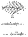
- Laminate 10 includes a pluralilty of layers, including a translucent substrate layer 12, a front translucent electrode layer 14, a reactive layer 16, and a rear electrode layer 18.
- the layers are advantageously deployed in Polymer Thick Film, or PTF, form.
- laminate 10 comprises a substrate layer 12 on which front translucent electrode layer 14 is deployed.
- substrate layer 12 may be any suitable material allowing the passage of visible light, such as polyester, polycarbonate, vinyl or elastomer.
- the substrate layer 12 in such embodiments will comprise a material that is at least partially translucent to such radiation.
- the layer 14 itself includes translucent electrode strips 20 and front insulator strips 22.
- the electrode strips 20 and the insulator strips 22 are positioned such that each electrode strip 20 is electrically isolated.
- Inks doped with a translucent conductive material and inks doped with an insulator such as a dielectric material may be deployed, for example using screen printing, to form the electrode strips 20 and insulator strips 22 included in front translucent electrode layer 14.
- the electrode strips 20 and the insulator strips 22 are arranged in a substantially straight, parallel alignment; however, it will be appreciated that the invention is not limited in this regard, and that other alignments are available, such as wavy, curved, spherical or other alignments.
- the translucent electrode strips 20 may be comprised of conductive ink and, in one embodiment, are deployed by screen printing. Other methods of deploying the translucent electrode strips 20 may include micro pen deposition, photo mask etching, electrostatic printing, rotary gravure, and hollow fibre deposition.
- the translucent electrode strips 20 may be in the range of five to seven microns thick and are advantageously positioned on spacings of up to 50 microns, although the invention is not limited in this regard if coarser or finer resolution is advantageous to the particular service. In order to resolve optimal detail in a human fingerprint, the translucent electrode strips 20 should be advantageously spaced less than 20 microns apart. Current CCD camera receptors generally resolve down to 9 microns. Accordingly, a reactive receptor according to the present invention in CCD service should provide translucent electrode strips 20 spaced about 9 microns apart.
- the invention is responsive to irradiated images of visible light
- the front translucent electrode layer 14 may comprise a translucent conductive material that is translucent to visible light, such as indium-tin-oxide.
- a translucent conductive material that is translucent to visible light
- suitable translucent conductive materials may act as the electrode material in the front translucent electrode layer 14, such as aluminum-tin-oxide or tantalum-tin-oxide, zinc-coated glass fibre, fine gold, or doped antimony.
- the front electrode strips 20 in such embodiments will comprise a material that is at least partially translucent to such radiation.
- Insulator strips 22, aligned between front translucent electrode strips 20, may comprise barium titanate, titanium dioxide or other suitable materials.
- FIGURE 1 also illustrates reactive layer 16 deployed adjacent to front translucent layer 14. It will be understood that a pattern of radiation, such as light, directed onto the reactive layer 16 will activate the reactive layer 16 in the areas of the layer actually exposed to radiation. Referring momentarily to FIGURE 4B , addressable zones 38 in the exposed areas of the reactive layer 16 will become activated and will generate detectable changes in state (e.g. resistance) that may be polled. It will be then appreciated that such polled changes in state may be advantageously represented as computer readable signals corresponding to the activated areas of the reactive layer 16.
- a pattern of radiation such as light
- reactive layer 16 is approximately 10-15 microns thick and is comprised of a vinyl or urethane carrier doped with a multi-crystal silicon, or with cadmium-telluride (n-type), or with cadmium-sulfide (p-type). P-n junctions are created within the reactive layer 16 which, when exposed to radiation, will generate an electrical charge.
- the reactive layer 16 may be doped with silver-sulfide which, when exposed to radiation, will exhibit a measurable resistive change. Materials such as cadmium-telluride and silver-sulfide are commonly available in the industry but can also be purchased from the Aldrich Company in 5 micron powder form.
- the reactive layer 16 may comprise a continuous layer over the front translucent electrode layer 14 as shown in FIGURE 4B .
- Common screen-printing, ink-jet printing, electrostatic deposition, rotary gravure, or rotary flexo techniques may be used to apply this layer of reactive material.
- the reactive layer 16 may comprise a plurality of discontinuous "regions" 36 of reactive material deployed at each region of intersection 34 where the translucent electrode strips 20 intersect the rear electrode strips 24.
- a preferred embodiment includes the rear electrode layer 18 deployed adjacent to the reactive layer 16.
- the rear electrode layer 18 comprises non-intersecting, alternating electrode strips 24 and insulator strips 26.
- Electrode strips 24 may be deployed by screen-printing techniques, or other methods such as micro pen deposition, photo mask etching, electrostatic printing, rotary gravure, or hollow fibre deposition, and may range from 1-50 microns wide and 8-10 microns thick.
- the deployed thicknesses of insulator strips 26 and electrode strips 24 are advantageously substantially the same. This assists in deployment of a rear electrode layer 18 that is substantially uniform in thickness.
- the rear electrode layer 18 and the front translucent electrode layer 14 are oriented relative to each other such that the translucent electrode strips 20 and the rear electrode strips 24 create array of regions of intersection 34 separated by the addressable zones 38 of reactive layer 16 shown in more detail on FIGURE 4B .
- FIGURES 4A and 4B illustrated on FIGURES 4A and 4B to be orthogonal, it will be understood that the invention is not limited in this regard It will be appreciated that, consistent with the invention, the front translucent electrode layer 14 and the rear electrode layer 18 may be oriented relative to each other in any orientation so long as an addressable array is formed by their regions of intersection 34.
- front translucent electrode strips 20 and rear electrode strips 24 may be of different widths and thicknesses and may feature different patterns or different arrangements of electrode strips, as illustrated in exemplary fashion on FIGURES 3A and 3B , in defining an addressable array of regions of intersection 34.
- the non-translucent rear electrode strips 24 of rear electrode layer 18 may comprise any suitable, conductive material, such as, for example, silver, graphite, copper (photo etched or in native form), metal oxide, or spherical glass in sub-micron form coated with metal to form a conductive powder.
- the insulator strips 26 comprise barium titinate.
- the layers 14, 16, and 18 of the inventive laminate 10 may be deployed using known technology.
- the laminate 10 may be assembled in the order as discussed above (e.g., the front electrode layer 14, deployed before the reactive layer which are deployed before the rear electrode layer 18), or reverse order of deployment may be equally advantageous.
- a sealing layer 28 may be added to protect the laminate and to seal it electrically.
- all layers in laminate 10 are advantageously screen printed, including the front translucent electrode layer 14, the reactive layer 16, and the rear electrode layer 18.
- discontinuous reactive regions 36 may preferably be ink-jet printed.
- the rear electrode strips 24 and the front translucent electrode strips 20 may also be photo-mask etched on sputtered polyester or some other suitable substrate.
- Some of the UV-curable, monolithic and membranous advantages of screen-printing may be adversely affected with etching, but photo-mask etching is known to achieve line widths down to 6 microns if such resolution is needed.
- a membranous structure using a unitary carrier is also a highly advantageous embodiment of the invention, particularly in the 3-dimensional embodiment depicted in FIGURE 5B , but it will be understood that the invention is not limited to this embodiment, or indeed to any of the foregoing embodiments described above.
- laminate 10 also may include a sealing layer 28 on top of the rear electrode layer.
- This sealing layer 28 is omitted from FIGURE 1 for clarity.
- the sealing layer 28 may comprise vinyl orurethane or any other suitable material translucent to the irradiated image being sensed. Sealing layer 28 is optional depending on the application in which the laminate 10 is used.
- FIGURE 2B is a similar cross-section to FIGURE 2A , illustrating an alternative embodiment of the invention.
- the rear electrode layer 18 is positioned adjacent to the substrate layer 12.
- the substrate layer 12 need not be translucent to the radiation to which the laminate 10 is exposed.
- an alternative embodiment of the disclosed invention features a reflective substrate layer 12 such that the irradiated image to which the laminate 10 is exposed may reflect back through the laminate 10 and further energize reactive layer 16 in selected addressable regions.
- FIGURES 2C and 2D show exemplary irradiated images, specifically a thumb print and a footprint, being received by an addressable receptor as disclosed herein.
- FIGURE 2C shows one embodiment of the disclosed invention where y-contacts 30 are connected to the rear electrode layer 18 (not shown) thereby providing the y-coordinates identifying the addressable zones 38 of the reactive layer 16 (not shown) selectively activated by the irradiated image.
- x-contacts 32 are connected to the front translucent electrode layer 14 (not shown) thereby providing the x-coordinates corresponding to the addressable zones 38 of the reactive layer 16 selectively activated by the irradiated image.
- the y-contacts 30 are connected to the front translucent electrode layer 14 and provide the y-coordinates for activated addressable zones 38 of the reactive layer 16.
- the x-contacts 32 are connected to the rear electrode layer 18 and provide the x-coordinates for the activated addressable zones 38 of the reactive layer 16.
- FIGURES 3A and 3B show plan views of two alternative embodiments in which front translucent electrode strips 20 and rear electrode strips 24 intersect to form irregularly-shaped arrays of electrode regions of intersection 34.
- FIGURE 3C is an orthographic view of an alternative embodiment in which rear electrode strips 24 and front translucent electrode strips 20 intersect to form a three-dimensional array of regions of intersection 34.
- FIGURE 4A shows an alternative embodiment comprising reactive regions 36 included in reactive layer 16.
- the reactive layer 16 is discontinuous and is comprised of reactive regions 36 deployed at the regions of intersection 34 between the front translucent electrode strips 20 and the rear electrode strips 24.
- reactive regions 36 are depicted on FIGURE 4A as circular, it will be understood that reactive regions 36 may be any suitable shape.
- Reactive regions 36 are surrounded by insulator material (not shown), such as barium titanate or other dielectric material.
- the reactive layer 16 comprising reactive regions 36 may advantageously be deployed at thicknesses ranging from 5-7 microns, although the invention is not limited in this regard.
- the reactive regions 36 illustrated in FIGURE 4A may be preferably deployed using ink-jet printing techniques commonly known in the art; however, any method of deploying the regions 36 may be used.
- a urethane carrier may be included in the ink comprising reactive regions 36 in the embodiment of FIGURE 4A ; however, the invention is again not limited in this regard.
- the reactive regions 36 may be deployed as dots with diameters of 5-15 microns; however, it will be appreciated that reactive regions 36 may be deployed in any suitable size
- Additional embodiments of the invention may use alternative techniques in deploying the reactive regions 36; such as, micro-pen or hollow fiber deposition.
- Hollow fiber deposition is known to inject material for deposition through a hollow fiber and then permit laser curing in situ.
- the reactive regions 36 are advantageously deployed first.
- the next step may be to print around the reactive regions 36 with a dielectric insulator material (not shown).
- a dielectric insulator material not shown.
- FIGURE 4B illustrates an alternative embodiment with reactive layer 16 in continuous layer form and of a sufficient thickness that the laminate 10 is able to provide "z-axis" conductivity properties as described above in the "Summary" section of this disclosure.
- addressable zones 38 of reactive layer 16 These addressable zones 38 correspond to areas where the front translucent electrode strips 20 and rear electrode strips 24 intersect to form regions of intersection 34 as illustrated on FIGURES 3A, 3B and 3C .
- a signal may be detected at the corresponding region of intersection 34 of electrode strips 20 and 24.
- a selected addressable zones 38 corresponding to the irradiated image will be activated, as depicted in exemplary fashion in FIGURES 2C and 2D discussed above.
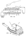
- FIGURE 5A is an elevation view of an image generator combined with a receptor laminate 10 as disclosed herein in two-dimensional deployment.
- a human thumb completes the circuit within the image generator and causes the luminescent layer to generate an irradiated image representing the human thumb.
- the light or other type of radiation from the image generator passes through the substrate layer 12, through the front translucent electrode layer 14 and into the reactive layer 16.
- the addressable zones 38 of the reactive layer 16 exposed to the irradiated image will react to the radiation.
- Front translucent electrode strips 20 and rear electrode strips 24 will detect the change in the reactive layer 16 at the addressable zones 38. Polling the state of addressable zones 38 via electrode strips 20 and 24 will enable a corresponding signal to be generated that is representative of the irradiated image.
- FIGURE 5B is an orthographic view of a combined image generator and receptor laminate 10 as in FIGURE 5A , except in three-dimensional deployment.
- This embodiment offers all of the features of the embodiment depicted in FIGURE 5A with the added advantage of being able to generate a signal representative of a three-dimensional image.
Landscapes
- Engineering & Computer Science (AREA)
- Human Computer Interaction (AREA)
- Physics & Mathematics (AREA)
- General Physics & Mathematics (AREA)
- Multimedia (AREA)
- Theoretical Computer Science (AREA)
- Laminated Bodies (AREA)
- Image Input (AREA)
- Devices For Indicating Variable Information By Combining Individual Elements (AREA)
Description
- This invention relates generally to the interpretation and conversion of irradiated images into electrical signals, and more specifically to an addressable Polymer Thick Film ("PTF") device that enables such interpretation and conversion.
- Devices are known in the art to capture images described by contact on a surface A primary, although by no means exclusive, application for such imaging devices is in the area of fingerprinting, whether for security, forensics or other purposes. Other applications include analysis of surface texture for classification or testing purposes, or recording contact for archival purposes, or possibly mechanical duplication.
- All of the foregoing applications involve translating the image described by contact into a reproducible record of the image. For example, in the fingerprint application, a time-honored system is to "ink" the fingers and roll them on a paper or card surface. Of course, without further scanning of the results, such systems lack the capability to generate computer-ready signals representative of the images. Without the storage and analysis capabilities of a computer, cataloging and comparison of such fingerprint images is a time-consuming and unpredictable task.
- More recent devices shine light onto the fingerprint via a prism. The reflected image may be captured on photosensitive film, or received onto a photosensitive array In the latter case, the image may then be pixelated and stored as an analog or digital signal representative of the image. These signals are now available for further processing by computers.
-
US-A-5,708,497 discloses a fingerprint image input apparatus including a two dimensional image sensor formed on transparent substrate and having a diffraction grating, photosensitive elements, switch elements, switching lines, signal reading lines, bias applying lines, and light interception plates disposed below photo-sensitive elements, a planar light source and a transparent protective film. The diffraction grating is formed on two-dimensional image sensor together with photo-sensitive elements commonly using one or more opaque materials of photo-sensitive elements. -
EP-A-0 901 093 discloses an image acquisition apparatus wherein light beam emitted by a surface illuminant reaches the surface of a transparent base layer of a recess/projection detection optical element. -
US-A-5,886,353 discloses an imaging device for producing images from electron-hole production radiation. Electron-hole pairs are produces in a radiation absorbing layer comprised of a photoconductive material. This layer covers an array of metal oxide semiconductor pixel circuits which are incorporated into and on a crystalline semiconductor substrate. -
WO 99/12472 - These and other objects, features and technical advantages are achieved by a sensor for fingerprinting as claimed in claim 1.
- The inventive laminate substantially comprises a rear conductive layer including a plurality of substantially parallel rear electrode strips, each of which is substantially electrically isolated, and an at least partially translucent front conductive layer also including a plurality of substantially parallel front electrode strips, each of which is also substantially electrically isolated. The front conductive layer is displaced angularly with respect to the rear conductive layer so that an array of electrode regions of intersection is formed corresponding to the regions at which the rear electrode strips cross over the front electrode strips.
- It will be noted that in the preferred embodiment described herein, the rear and front electrode strips are disclosed substantially straight and substantially perpendicular to each other for ease of illustration and description. It will nonetheless be understood that the invention is not limited in this regard. Consistent with the scope of the invention, the rear and front electrode strips may each follow any desired curved or contoured pattern, in two or three dimensions, so long as the strips run substantially parallel within the pattern, and so long as when superposed, the real and front electrode strips intersect to form a definable array of electrode regions of intersection.
- The rear and front conductive layers in the inventive laminate are separated by a reactive layer By "reactive," it will be understood that portions of the layer generate electrical impulses, or undergo resistive change, when exposed to radiation in the electromagnetic spectrum While a preferred embodiment of the invention contemplates a photosensitive layer that is reactive to visible light, it will be understood that the invention is not limited just to photosensitive performance, and other types of reactive layer that may be also responsive to radiation outside the visible spectrum are within the scope of the claims.
- Alternative deployments of the reactive layer are disclosed. In a first deployment, the reactive layer comprises a plurality of discrete and substantially electrically isolated reactive regions Non-conductive filler, such as a dielectric, surrounds the reactive regions to isolate them. The reactive regions are deployed in a reactive array substantially in register with the array of electrode regions of intersection The reactive regions thus become electrically addressable by coordinate pairs of rear and front electrode strips. In a second embodiment, the reactive layer comprises a unitary layer of substantially uninterrupted reactive material commonly separating rear and front electrode strips at multiple, and in many cases, all of the electrode regions of intersection. The reactive material in the unitary layer in this second embodiment also advantageously possesses "Z-axis" properties, meaning that its structural properties allow electrical pathways only in a direction through the "thickness of the laminate," ie orthogonal to the plane of the laminate. The electrode regions of intersection in this second embodiment thus define "zones" in the unitary reactive layer that are addressable by the respective coordinate pairs of rear and front electrodes. The size of the zones tends to correspond substantially to the size of the intersecting area of electrode strips, especially if the reactive material possesses strong "Z-axis" properties. The width of the intersecting electrode strips and their angle of intersection thus influence the size of the addressable reactive zones.
- Non-conductive filler material is interposed between the front electrode strips to ensure substantial electrical isolation Other advantages of interposing non-conductive filler between the front electrode strips are described below Non conductive filler is also advantageously interposed between rear electrode strips, although design criteria may arise when such filler may be omitted. Non-conductive filler materials are well known. In the preferred embodiment, an exemplary suitable non-conductive filler material is a dielectric such as barium-titanate or titanium-dioxide. The non-conductive filler material may advantageously be deployed using a methane carrier, and further advantageously using a UV-curable methane carrier, bringing additional advantages.
- As noted, the preferred embodiment of the invention is responsive to irradiated images of visible light, although the invention is not limited in this regard. Accordingly, the front electrode strips comprise an electrode material that is translucent at least to visible light, such as indium-tin-oxide The rear electrode strips may be made from well-known conductive materials that are opaque to light, such as, for example, silver, graphite or copper. Silver is particularly advantageous in the rear electrode strips because of its reflective properties. In embodiments where the inventive receptor is responsive to other wavelengths of radiation outside the visible spectrum, it will be understood that the front electrode strips in such embodiments will comprise a material that is at least partially translucent to such radiation.
- The reactive regions comprise an active ingredient selected to generate electric potential or resistive change when exposed to radiation in a specific wavelength range. In the preferred embodiment responsive to irradiated images of visible light, exemplary active ingredients include multi-crystal silicon, cadmium-telluride (n-type) or cadmium-sulfide (p-type) in a p-n junction format, although it will be appreciated that many reactive materials are known and available as alternative active ingredients responsive to radiation above, below and including the visible spectrum. Alternatively, use of silver-sulfide in the p-n junction in the reactive layer will bring about resistive change upon exposure to radiation.
- It is therefore a technical advantage of the present invention to generate a digital signal representative of an irradiated image. In operation, an irradiated image is directed onto the receptor laminate. In the preferred embodiment responsive to visible light, the irradiated pattern passes through the translucent front electrode strips and selectively energizes the reactive layer in a corresponding pattern. Where energized, the reactive regions or zones generate electric potential (or alternatively resistive change) across the coordinate pairs of electrode strips addressed thereby. The condition of all of the reactive regions or zones (i.e. the reactive array) is periodically sampled by polling a series of predetermined sequences of coordinate pairs of electrode strips. The polled value of the electrical potential across specific coordinate pairs in the series of sequences defines the current energized (or resistive) state ofthe reactive array, and thus may be used to generate a corresponding digital signal representative of the condition of the reactive array. Such a digital signal may thus be captured as a computer-readable representation of the irradiated image directed onto the reactive receptor. Here again, two alternative embodiments are disclosed. In one embodiment, the polling merely detects the existence of electrical potential (or resistive change) at coordinate pairs of electrode strips, Such information may be used to generate a digital signal corresponding to a two-tone representation ofthe irradiated image. In a second embodiment, the polling further measures the value of electrical potential (or resistive change) at coordinate pairs of electrode strips. Such additional data may be used to enrich the corresponding digital signal with gray-scale information.
- Another technical advantage of the present invention is that it is immediately compatible with image-generating laminates. In fact, the reactive receptor laminate of the present invention may be combined with an image-generating laminate to form a combined unitary laminate assembly.
- This combined generator/receptor assembly will be immediately seen to have added advantages in that it is a self-contained laminate capable of generating a digital signals representative of a pattern of contact.
- A further advantage of the present invention is that, when desired, the reactive receptor laminate may be fabricated so as to achieve membranous properties in rapid-cure form. Such receptor laminates will then be immediately compatible with sources of irradiated images contoured into three dimensions.
- A still further technical advantage of the present invention is that it is scalable.. Alternative techniques available to be used in construction of the receptor laminate may be selected according to the reactive array resolution desired. Embodiments described herein teach a number of exemplary combinations of construction techniques designed to achieve varying levels of reactive array resolution.
- The foregoing has outlined rather broadly the features and technical advantages of the present invention in order that the detailed description of the invention that follows may be better understood. Additional features and advantages of the invention will be described hereinafter which form the subject of the claims of the invention. It should be appreciated by those skilled in the art that the conception and the specific embodiment disclosed may be readily utilized as a basis for modifying or designing other structures for carrying out the same purposes of the present invention. It should also be realized by those skilled in the art that such equivalent constructions do not depart from the spirit and scope of the invention as set forth in the appended claims.
- For a more complete understanding of the present invention, and the advantages thereof, reference is now made to the following descriptions taken in conjunction with the accompanying drawings, in which:
-
FIGURE 1 is a cutaway view of one embodiment of the present invention. -
FIGURE 2A is section view as shown onFIGURE 1 . -
FIGURE 2B is a section view through an alternative embodiment of the present invention. -
FIGURES 2C and 2D depict the invention in operation. -
FIGURES 3A and 3B are plan views of two alternative embodiments of the present invention depicting different electrode array patterns. -
FIGURE 3C is an orthographic view of a three-dimensional embodiment of the present invention. -
FIGURE 4A is a cutaway view of one embodiment of the present invention. -
FIGURE 4B is a cutaway view of an alternative embodiment ofthe present invention. -
FIGURE 5A is a section view of a two-dimensional embodiment of the present invention in use. -
FIGURE 5B is an orthographic view of a three-dimensional embodiment of the present invention in use. - As described summarily above, the present invention comprises an apparatus disposed to receive irradiated images and generate electrical signals which correspond to the received image. Advantageously, the signals are computer-readable. A preferred embodiment includes a membranous PTF laminate comprising urethane and UV-curable inks. The preferred embodiment further includes an array of regions addressed by conductive material, with reactive material located at the addressable regions of the array. When selectively activated or stimulated, the addressable reactive material is disposed to generate signals, advantageously computer-readable, representative of an irradiated image causing such selective activation or stimulation.
- Turning now to
FIGURE 1 , a general arrangement of a first embodiment is illustrated.Laminate 10 includes a pluralilty of layers, including atranslucent substrate layer 12, a fronttranslucent electrode layer 14, areactive layer 16, and arear electrode layer 18. In the embodiment ofFIGURE 1 , the layers are advantageously deployed in Polymer Thick Film, or PTF, form. - With further reference to
FIGURE 1 ,laminate 10 comprises asubstrate layer 12 on which fronttranslucent electrode layer 14 is deployed. In a preferred embodiment,substrate layer 12 may be any suitable material allowing the passage of visible light, such as polyester, polycarbonate, vinyl or elastomer. In embodiments where the inventive receptor is responsive to other wavelengths or radiation outside the visible spectrum, it will be understood that thesubstrate layer 12 in such embodiments will comprise a material that is at least partially translucent to such radiation. - With respect to the front
translucent electrode layer 14, thelayer 14 itself includes translucent electrode strips 20 and front insulator strips 22. The electrode strips 20 and the insulator strips 22 are positioned such that eachelectrode strip 20 is electrically isolated. Inks doped with a translucent conductive material and inks doped with an insulator such as a dielectric material may be deployed, for example using screen printing, to form the electrode strips 20 and insulator strips 22 included in fronttranslucent electrode layer 14. In the embodiment ofFIGURE 1 , the electrode strips 20 and the insulator strips 22 are arranged in a substantially straight, parallel alignment; however, it will be appreciated that the invention is not limited in this regard, and that other alignments are available, such as wavy, curved, spherical or other alignments. - As noted, the translucent electrode strips 20 may be comprised of conductive ink and, in one embodiment, are deployed by screen printing. Other methods of deploying the translucent electrode strips 20 may include micro pen deposition, photo mask etching, electrostatic printing, rotary gravure, and hollow fibre deposition. The translucent electrode strips 20 may be in the range of five to seven microns thick and are advantageously positioned on spacings of up to 50 microns, although the invention is not limited in this regard if coarser or finer resolution is advantageous to the particular service. In order to resolve optimal detail in a human fingerprint, the translucent electrode strips 20 should be advantageously spaced less than 20 microns apart. Current CCD camera receptors generally resolve down to 9 microns. Accordingly, a reactive receptor according to the present invention in CCD service should provide translucent electrode strips 20 spaced about 9 microns apart.
- In a preferred embodiment, the invention is responsive to irradiated images of visible light, thus the front
translucent electrode layer 14 may comprise a translucent conductive material that is translucent to visible light, such as indium-tin-oxide. Other suitable translucent conductive materials may act as the electrode material in the fronttranslucent electrode layer 14, such as aluminum-tin-oxide or tantalum-tin-oxide, zinc-coated glass fibre, fine gold, or doped antimony. In embodiments where the inventive receptor is responsive to other wavelengths or radiation outside the visible spectrum, it will be understood that the front electrode strips 20 in such embodiments will comprise a material that is at least partially translucent to such radiation. Insulator strips 22, aligned between front translucent electrode strips 20, may comprise barium titanate, titanium dioxide or other suitable materials. -
FIGURE 1 also illustratesreactive layer 16 deployed adjacent to fronttranslucent layer 14. It will be understood that a pattern of radiation, such as light, directed onto thereactive layer 16 will activate thereactive layer 16 in the areas of the layer actually exposed to radiation. Referring momentarily toFIGURE 4B ,addressable zones 38 in the exposed areas of thereactive layer 16 will become activated and will generate detectable changes in state (e.g. resistance) that may be polled. It will be then appreciated that such polled changes in state may be advantageously represented as computer readable signals corresponding to the activated areas of thereactive layer 16. - In a preferred embodiment,
reactive layer 16 is approximately 10-15 microns thick and is comprised of a vinyl or urethane carrier doped with a multi-crystal silicon, or with cadmium-telluride (n-type), or with cadmium-sulfide (p-type). P-n junctions are created within thereactive layer 16 which, when exposed to radiation, will generate an electrical charge. Alternatively, thereactive layer 16 may be doped with silver-sulfide which, when exposed to radiation, will exhibit a measurable resistive change. Materials such as cadmium-telluride and silver-sulfide are commonly available in the industry but can also be purchased from the Aldrich Company in 5 micron powder form. - Referring briefly to
FIGURES 4A and 4B , thereactive layer 16 may comprise a continuous layer over the fronttranslucent electrode layer 14 as shown inFIGURE 4B . Common screen-printing, ink-jet printing, electrostatic deposition, rotary gravure, or rotary flexo techniques may be used to apply this layer of reactive material. Alternatively, as depicted inFIGURE 4A , thereactive layer 16 may comprise a plurality of discontinuous "regions" 36 of reactive material deployed at each region ofintersection 34 where the translucent electrode strips 20 intersect the rear electrode strips 24. - With further reference to
FIGURE 1 , a preferred embodiment includes therear electrode layer 18 deployed adjacent to thereactive layer 16. Analogous to fronttranslucent electrode layer 14, therear electrode layer 18 comprises non-intersecting, alternating electrode strips 24 and insulator strips 26. Electrode strips 24 may be deployed by screen-printing techniques, or other methods such as micro pen deposition, photo mask etching, electrostatic printing, rotary gravure, or hollow fibre deposition, and may range from 1-50 microns wide and 8-10 microns thick. The deployed thicknesses of insulator strips 26 and electrode strips 24 are advantageously substantially the same. This assists in deployment of arear electrode layer 18 that is substantially uniform in thickness. - Referring briefly to
FIGURES 3A and 3B , therear electrode layer 18 and the fronttranslucent electrode layer 14 are oriented relative to each other such that the translucent electrode strips 20 and the rear electrode strips 24 create array of regions ofintersection 34 separated by theaddressable zones 38 ofreactive layer 16 shown in more detail onFIGURE 4B . Although illustrated onFIGURES 4A and 4B to be orthogonal, it will be understood that the invention is not limited in this regard It will be appreciated that, consistent with the invention, the fronttranslucent electrode layer 14 and therear electrode layer 18 may be oriented relative to each other in any orientation so long as an addressable array is formed by their regions ofintersection 34. It will be appreciated further that front translucent electrode strips 20 and rear electrode strips 24 may be of different widths and thicknesses and may feature different patterns or different arrangements of electrode strips, as illustrated in exemplary fashion onFIGURES 3A and 3B , in defining an addressable array of regions ofintersection 34. - The non-translucent rear electrode strips 24 of
rear electrode layer 18 may comprise any suitable, conductive material, such as, for example, silver, graphite, copper (photo etched or in native form), metal oxide, or spherical glass in sub-micron form coated with metal to form a conductive powder. With respect to the rear insulator strips 26, in a preferred embodiment, the insulator strips 26 comprise barium titinate. - The
layers inventive laminate 10 may be deployed using known technology. The laminate 10 may be assembled in the order as discussed above (e.g., thefront electrode layer 14, deployed before the reactive layer which are deployed before the rear electrode layer 18), or reverse order of deployment may be equally advantageous. Asealing layer 28 may be added to protect the laminate and to seal it electrically. - In a preferred embodiment, all layers in
laminate 10 are advantageously screen printed, including the fronttranslucent electrode layer 14, thereactive layer 16, and therear electrode layer 18. In an alternative embodiment disclosed inFIGURE 4A and discussed below. However, discontinuousreactive regions 36 may preferably be ink-jet printed. - In other embodiments, the rear electrode strips 24 and the front translucent electrode strips 20 may also be photo-mask etched on sputtered polyester or some other suitable substrate. Some of the UV-curable, monolithic and membranous advantages of screen-printing may be adversely affected with etching, but photo-mask etching is known to achieve line widths down to 6 microns if such resolution is needed. A membranous structure using a unitary carrier is also a highly advantageous embodiment of the invention, particularly in the 3-dimensional embodiment depicted in
FIGURE 5B , but it will be understood that the invention is not limited to this embodiment, or indeed to any of the foregoing embodiments described above. - Turning now to
FIGURE 2A , a cross section as shown onFIGURE 1 is shown. It will be seen onFIGURE 2A that laminate 10 also may include asealing layer 28 on top of the rear electrode layer. Thissealing layer 28 is omitted fromFIGURE 1 for clarity. Thesealing layer 28 may comprise vinyl orurethane or any other suitable material translucent to the irradiated image being sensed. Sealinglayer 28 is optional depending on the application in which the laminate 10 is used. -
FIGURE 2B is a similar cross-section toFIGURE 2A , illustrating an alternative embodiment of the invention. In this embodiment, therear electrode layer 18 is positioned adjacent to thesubstrate layer 12. In this arrangement, thesubstrate layer 12 need not be translucent to the radiation to which the laminate 10 is exposed. In fact, an alternative embodiment of the disclosed invention features areflective substrate layer 12 such that the irradiated image to which the laminate 10 is exposed may reflect back through the laminate 10 and further energizereactive layer 16 in selected addressable regions. -
FIGURES 2C and 2D show exemplary irradiated images, specifically a thumb print and a footprint, being received by an addressable receptor as disclosed herein.FIGURE 2C shows one embodiment of the disclosed invention where y-contacts 30 are connected to the rear electrode layer 18 (not shown) thereby providing the y-coordinates identifying theaddressable zones 38 of the reactive layer 16 (not shown) selectively activated by the irradiated image. Similarly, x-contacts 32 are connected to the front translucent electrode layer 14 (not shown) thereby providing the x-coordinates corresponding to theaddressable zones 38 of thereactive layer 16 selectively activated by the irradiated image. In another embodiment shown inFIGURE 2D , the y-contacts 30 are connected to the fronttranslucent electrode layer 14 and provide the y-coordinates for activatedaddressable zones 38 of thereactive layer 16. Similarly, the x-contacts 32 are connected to therear electrode layer 18 and provide the x-coordinates for the activatedaddressable zones 38 of thereactive layer 16. -
FIGURES 3A and 3B show plan views of two alternative embodiments in which front translucent electrode strips 20 and rear electrode strips 24 intersect to form irregularly-shaped arrays of electrode regions ofintersection 34. -
FIGURE 3C is an orthographic view of an alternative embodiment in which rear electrode strips 24 and front translucent electrode strips 20 intersect to form a three-dimensional array of regions ofintersection 34. - As discussed above,
FIGURE 4A shows an alternative embodiment comprisingreactive regions 36 included inreactive layer 16. In this embodiment, thereactive layer 16 is discontinuous and is comprised ofreactive regions 36 deployed at the regions ofintersection 34 between the front translucent electrode strips 20 and the rear electrode strips 24. Note that althoughreactive regions 36 are depicted onFIGURE 4A as circular, it will be understood thatreactive regions 36 may be any suitable shape.Reactive regions 36 are surrounded by insulator material (not shown), such as barium titanate or other dielectric material. In a PTF embodiment, thereactive layer 16 comprisingreactive regions 36 may advantageously be deployed at thicknesses ranging from 5-7 microns, although the invention is not limited in this regard. - The
reactive regions 36 illustrated inFIGURE 4A may be preferably deployed using ink-jet printing techniques commonly known in the art; however, any method of deploying theregions 36 may be used. Preferably, a urethane carrier may be included in the ink comprisingreactive regions 36 in the embodiment ofFIGURE 4A ; however, the invention is again not limited in this regard. By using ink-jet technology, thereactive regions 36 may be deployed as dots with diameters of 5-15 microns; however, it will be appreciated thatreactive regions 36 may be deployed in any suitable size - Additional embodiments of the invention may use alternative techniques in deploying the
reactive regions 36; such as, micro-pen or hollow fiber deposition. Hollow fiber deposition is known to inject material for deposition through a hollow fiber and then permit laser curing in situ. - When
reactive layer 16 is in discontinuous region form, such as illustrated inFIGURE 4A , thereactive regions 36 are advantageously deployed first. The next step may be to print around thereactive regions 36 with a dielectric insulator material (not shown). Such selective printing techniques are well known in the screen printing art. -
FIGURE 4B illustrates an alternative embodiment withreactive layer 16 in continuous layer form and of a sufficient thickness that the laminate 10 is able to provide "z-axis" conductivity properties as described above in the "Summary" section of this disclosure. Also shown inFIGURE 4B areaddressable zones 38 ofreactive layer 16. Theseaddressable zones 38 correspond to areas where the front translucent electrode strips 20 and rear electrode strips 24 intersect to form regions ofintersection 34 as illustrated onFIGURES 3A, 3B and3C . When thereactive layer 16 is activated at one of theseaddressable zones 38, a signal may be detected at the corresponding region ofintersection 34 of electrode strips 20 and 24. When an irradiated image is exposed to the laminate 10, a selectedaddressable zones 38 corresponding to the irradiated image will be activated, as depicted in exemplary fashion inFIGURES 2C and 2D discussed above. -
FIGURE 5A is an elevation view of an image generator combined with areceptor laminate 10 as disclosed herein in two-dimensional deployment. As is shown inFIGURE 5A , a human thumb completes the circuit within the image generator and causes the luminescent layer to generate an irradiated image representing the human thumb. The light or other type of radiation from the image generator passes through thesubstrate layer 12, through the fronttranslucent electrode layer 14 and into thereactive layer 16. Theaddressable zones 38 of thereactive layer 16 exposed to the irradiated image will react to the radiation. Front translucent electrode strips 20 and rear electrode strips 24 will detect the change in thereactive layer 16 at theaddressable zones 38. Polling the state ofaddressable zones 38 via electrode strips 20 and 24 will enable a corresponding signal to be generated that is representative of the irradiated image. -
FIGURE 5B is an orthographic view of a combined image generator andreceptor laminate 10 as inFIGURE 5A , except in three-dimensional deployment. This embodiment offers all of the features of the embodiment depicted inFIGURE 5A with the added advantage of being able to generate a signal representative of a three-dimensional image. - Techniques of sampling or polling arrays of interconnected electrodes are well known in the art and may be useful to create a digital signal representative of the irradiated image. Also, techniques are known in the art for converting the current state of a polled or sampled array into a representative digital signal suitable for processing by digital processors.
- Although the present invention and its advantages have been described in detail, it should be understood that various changes, substitutions and alterations can be made herein without departing from the scope of the invention as defined by the appended claims.
Claims (12)
- A sensor for fingerprinting, comprising:a polymer thick film translucent substrate layer (12);a polymer thick film rear conductive layer (18) including a plurality of substantially parallel rear electrode strips (24), each of the rear electrode strips (24) being individually substantially electrically isolated;a polymer thick film front conductive layer (14) disposed on the substrate layer (12) and including a plurality of substantially parallel front electrode strips (20), each of the front electrode strips (20) being individually substantially electrically isolated, wherein a plurality of the front electrode strips (20) comprise an electrically-conductive material that is at least partially transparent to visible light; andthe front conductive layer (14) superposed over the rear conductive layer (18) and oriented with respect thereto so as to form overlapping areas (34) at which the rear electrode strips (24) cross over the front electrode strips (20) characterized by:the rear (18) and front (14) conductive layers separated by a light reactive layer (16), the light reactive layer (16) comprising a plurality of predetermined regions (38) that generate electrical impulses when exposed to visible light, the said regions (38) being located in the overlapping areas (34) between the rear electrode strips (24) and the front electrode strips (20) so that the regions (38) are electrically addressable by coordinate pairs of rear (24) and front (20) electrode strips.
- The sensor of claim 1, in which the front conductive layer (14) is oriented substantially perpendicularly with respect to the rear conductive layer (18).
- The sensor of claim 1, in which the plurality of front electrode strips (20) comprise material selected from the group consisting of:(a) indium-tin-oxide;(b) aluminum-tin-oxide;(c) zinc-coated glass fibre;(d) gold;(e) doped antimony; and(f) tantalum-tin-oxide.
- The sensor of claim 1, in which the rear electrode strips (24) are substantially electrically isolated via intervening strips of non-conductive filler (26).
- The sensor of claim 1, in which the front electrode strips (20) are substantially electrically isolated via intervening strips of non-conductive filler (22).
- The sensor of claim 1, in which the light reactive layer (16) is deposited using a process selected from the group consisting of:(a) ink jet printing;(b) screen printing;(c) electrostatic deposition;(d) rotary gravure;(e) rotary flexo;(f) micro pen; and(g) hollow fiber pen.
- The sensor of claim 1, in which the regions (38) comprise material selected from the group consisting of:(a) multi-crystal silicon;(b) cadmium-telluride;(c) cadmium-sulfide; and(d) silver-sulfide.
- The sensor of claim 1, in which selected ones of the rear (24) and front (20) electrode strips are deposited using a process selected from the group consisting of:(a) screen printing;(b) micro pen deposition;(c) photo-mask etching;(d) electrostatic printing;(e) rotary gravure; and(f) hollow fibre deposition.
- The sensor of claim 1, in which the rear (24) and front (20) electrode strips are of substantially equal width in the range of 1-50 microns.
- The sensor of claim 1, in which a plurality of the rear electrode strips (24) comprise a material selected from the group consisting of:(a) silver;(b) graphite;(c) copper;(d) metal-coated glass; and(e) a metal oxide.
- The sensor of claim 1, in which at least one of the rear (18) and front (14) conductive layers deploys electrode strips in a pattern containing curves.
- The sensor of claim 1, in which the rear (18) and front (14) conductive layers deploy electrode strips in a three-dimensional contoured shape.
Applications Claiming Priority (3)
| Application Number | Priority Date | Filing Date | Title |
|---|---|---|---|
| US25856600P | 2000-12-27 | 2000-12-27 | |
| US258566P | 2000-12-27 | ||
| PCT/US2001/050573 WO2002052484A2 (en) | 2000-12-27 | 2001-12-21 | Addressable ptf receptor for irradiated images |
Publications (3)
| Publication Number | Publication Date |
|---|---|
| EP1410308A2 EP1410308A2 (en) | 2004-04-21 |
| EP1410308A4 EP1410308A4 (en) | 2007-12-19 |
| EP1410308B1 true EP1410308B1 (en) | 2013-04-10 |
Family
ID=22981123
Family Applications (1)
| Application Number | Title | Priority Date | Filing Date |
|---|---|---|---|
| EP01987503.8A Expired - Lifetime EP1410308B1 (en) | 2000-12-27 | 2001-12-21 | Addressable ptf receptor for irradiated images |
Country Status (4)
| Country | Link |
|---|---|
| US (1) | US6936335B2 (en) |
| EP (1) | EP1410308B1 (en) |
| AU (1) | AU2002239708A1 (en) |
| WO (1) | WO2002052484A2 (en) |
Families Citing this family (3)
| Publication number | Priority date | Publication date | Assignee | Title |
|---|---|---|---|---|
| US20070132367A1 (en) * | 2003-11-03 | 2007-06-14 | Emil Enz | Electroluminescence system |
| AT413896B (en) * | 2004-09-08 | 2006-07-15 | Nanoident Technologies Ag | DEVICE FOR DETECTING A FINGERPRINT |
| CN106462285B (en) * | 2014-04-10 | 2020-06-09 | Ib韩国有限责任公司 | Biometric sensor for touch device |
Family Cites Families (11)
| Publication number | Priority date | Publication date | Assignee | Title |
|---|---|---|---|---|
| US4394773A (en) * | 1980-07-21 | 1983-07-19 | Siemens Corporation | Fingerprint sensor |
| JP3378032B2 (en) * | 1992-08-28 | 2003-02-17 | 浜松ホトニクス株式会社 | Person verification device |
| US5886353A (en) * | 1995-04-21 | 1999-03-23 | Thermotrex Corporation | Imaging device |
| US5708497A (en) | 1995-08-15 | 1998-01-13 | Nec Corporation | Fingerprint image input apparatus and method of producing the same |
| US5856029A (en) * | 1996-05-30 | 1999-01-05 | E.L. Specialists, Inc. | Electroluminescent system in monolithic structure |
| US6205690B1 (en) * | 1996-07-23 | 2001-03-27 | Xs Energy International, Inc. | Panels with animation and sound |
| US5856030A (en) * | 1996-12-30 | 1999-01-05 | E.L. Specialists, Inc. | Elastomeric electroluminescent lamp |
| US6310683B1 (en) * | 1997-08-05 | 2001-10-30 | Casio Computer Co., Ltd. | Apparatus for reading fingerprint |
| US6856383B1 (en) | 1997-09-05 | 2005-02-15 | Security First Corp. | Relief object image generator |
| US6091838A (en) * | 1998-06-08 | 2000-07-18 | E.L. Specialists, Inc. | Irradiated images described by electrical contact |
| US6411726B1 (en) * | 1998-10-08 | 2002-06-25 | Durel Corporation | Fingerprint detector using an EL lamp |
-
2001
- 2001-12-21 EP EP01987503.8A patent/EP1410308B1/en not_active Expired - Lifetime
- 2001-12-21 AU AU2002239708A patent/AU2002239708A1/en not_active Abandoned
- 2001-12-21 US US10/450,708 patent/US6936335B2/en not_active Expired - Lifetime
- 2001-12-21 WO PCT/US2001/050573 patent/WO2002052484A2/en not_active Application Discontinuation
Also Published As
| Publication number | Publication date |
|---|---|
| WO2002052484A2 (en) | 2002-07-04 |
| WO2002052484A3 (en) | 2004-01-08 |
| AU2002239708A1 (en) | 2002-07-08 |
| EP1410308A2 (en) | 2004-04-21 |
| US20040067393A1 (en) | 2004-04-08 |
| US6936335B2 (en) | 2005-08-30 |
| EP1410308A4 (en) | 2007-12-19 |
Similar Documents
| Publication | Publication Date | Title |
|---|---|---|
| CA2334620C (en) | Irradiated images described by electrical contact | |
| US5243332A (en) | Information entry and display | |
| US5565657A (en) | Multidimensional user interface input device | |
| US8253696B2 (en) | Flexible fingerprint sensor | |
| EP3678053B1 (en) | Fingerprint sensor and display device including the same | |
| US5325167A (en) | Record document authentication by microscopic grain structure and method | |
| EP1018698B1 (en) | Static charge dissipation for an active circuit surface | |
| US6478976B1 (en) | Apparatus and method for contacting a conductive layer | |
| US5723204A (en) | Two-sided electrical paper | |
| EP1018696A2 (en) | Static charge dissipation pads for sensors | |
| KR20010012635A (en) | Fingerprint sensor with gain control features and associated methods | |
| EP1469378A1 (en) | Position detection apparatus | |
| EP1410308B1 (en) | Addressable ptf receptor for irradiated images | |
| EP0575187B1 (en) | Image sensor | |
| WO1995004665A1 (en) | Embedded printed data - method and apparatus | |
| EP0119742B2 (en) | Two-dimensional image readout device | |
| EP0441567A2 (en) | Pressure sensitive device | |
| EP1154489B1 (en) | Bispectral optical detector | |
| JP2003517646A (en) | Structure of safety element with optical diffraction effect and control device for such element | |
| US20020056812A1 (en) | Irradiated images described by electrical contact in three dimensions | |
| US4788593A (en) | High resolution scanning system including optical enlargement | |
| MXPA01006039A (en) | Irradiated images described by electrical contact in three dimensions |
Legal Events
| Date | Code | Title | Description |
|---|---|---|---|
| PUAI | Public reference made under article 153(3) epc to a published international application that has entered the european phase |
Free format text: ORIGINAL CODE: 0009012 |
|
| 17P | Request for examination filed |
Effective date: 20030702 |
|
| AK | Designated contracting states |
Kind code of ref document: A2 Designated state(s): AT DE |
|
| RAP1 | Party data changed (applicant data changed or rights of an application transferred) |
Owner name: ORYONTECHNOLOGIES, LLC |
|
| A4 | Supplementary search report drawn up and despatched |
Effective date: 20071121 |
|
| RIC1 | Information provided on ipc code assigned before grant |
Ipc: G06K 9/00 20060101ALI20071115BHEP Ipc: G06K 1/00 20060101AFI20020710BHEP |
|
| 17Q | First examination report despatched |
Effective date: 20080310 |
|
| GRAP | Despatch of communication of intention to grant a patent |
Free format text: ORIGINAL CODE: EPIDOSNIGR1 |
|
| RBV | Designated contracting states (corrected) |
Designated state(s): DE |
|
| GRAS | Grant fee paid |
Free format text: ORIGINAL CODE: EPIDOSNIGR3 |
|
| GRAA | (expected) grant |
Free format text: ORIGINAL CODE: 0009210 |
|
| AK | Designated contracting states |
Kind code of ref document: B1 Designated state(s): DE |
|
| REG | Reference to a national code |
Ref country code: DE Ref legal event code: R096 Ref document number: 60147865 Country of ref document: DE Effective date: 20130606 |
|
| PLBE | No opposition filed within time limit |
Free format text: ORIGINAL CODE: 0009261 |
|
| STAA | Information on the status of an ep patent application or granted ep patent |
Free format text: STATUS: NO OPPOSITION FILED WITHIN TIME LIMIT |
|
| 26N | No opposition filed |
Effective date: 20140113 |
|
| REG | Reference to a national code |
Ref country code: DE Ref legal event code: R097 Ref document number: 60147865 Country of ref document: DE Effective date: 20140113 |
|
| REG | Reference to a national code |
Ref country code: DE Ref legal event code: R082 Ref document number: 60147865 Country of ref document: DE Representative=s name: VIERING, JENTSCHURA & PARTNER MBB PATENT- UND , DE |
|
| PGFP | Annual fee paid to national office [announced via postgrant information from national office to epo] |
Ref country code: DE Payment date: 20190628 Year of fee payment: 18 |
|
| REG | Reference to a national code |
Ref country code: DE Ref legal event code: R119 Ref document number: 60147865 Country of ref document: DE |
|
| PG25 | Lapsed in a contracting state [announced via postgrant information from national office to epo] |
Ref country code: DE Free format text: LAPSE BECAUSE OF NON-PAYMENT OF DUE FEES Effective date: 20200701 |