EP1387392B1 - Electrostatic gripper - Google Patents
Electrostatic gripper Download PDFInfo
- Publication number
- EP1387392B1 EP1387392B1 EP03000853.6A EP03000853A EP1387392B1 EP 1387392 B1 EP1387392 B1 EP 1387392B1 EP 03000853 A EP03000853 A EP 03000853A EP 1387392 B1 EP1387392 B1 EP 1387392B1
- Authority
- EP
- European Patent Office
- Prior art keywords
- gripping device
- wafer
- circuit board
- gripping
- electrodes
- Prior art date
- Legal status (The legal status is an assumption and is not a legal conclusion. Google has not performed a legal analysis and makes no representation as to the accuracy of the status listed.)
- Expired - Lifetime
Links
Images

Classifications
-
- H—ELECTRICITY
- H01—ELECTRIC ELEMENTS
- H01L—SEMICONDUCTOR DEVICES NOT COVERED BY CLASS H10
- H01L21/00—Processes or apparatus adapted for the manufacture or treatment of semiconductor or solid state devices or of parts thereof
- H01L21/67—Apparatus specially adapted for handling semiconductor or electric solid state devices during manufacture or treatment thereof; Apparatus specially adapted for handling wafers during manufacture or treatment of semiconductor or electric solid state devices or components ; Apparatus not specifically provided for elsewhere
- H01L21/683—Apparatus specially adapted for handling semiconductor or electric solid state devices during manufacture or treatment thereof; Apparatus specially adapted for handling wafers during manufacture or treatment of semiconductor or electric solid state devices or components ; Apparatus not specifically provided for elsewhere for supporting or gripping
- H01L21/6831—Apparatus specially adapted for handling semiconductor or electric solid state devices during manufacture or treatment thereof; Apparatus specially adapted for handling wafers during manufacture or treatment of semiconductor or electric solid state devices or components ; Apparatus not specifically provided for elsewhere for supporting or gripping using electrostatic chucks
-
- Y—GENERAL TAGGING OF NEW TECHNOLOGICAL DEVELOPMENTS; GENERAL TAGGING OF CROSS-SECTIONAL TECHNOLOGIES SPANNING OVER SEVERAL SECTIONS OF THE IPC; TECHNICAL SUBJECTS COVERED BY FORMER USPC CROSS-REFERENCE ART COLLECTIONS [XRACs] AND DIGESTS
- Y10—TECHNICAL SUBJECTS COVERED BY FORMER USPC
- Y10T—TECHNICAL SUBJECTS COVERED BY FORMER US CLASSIFICATION
- Y10T279/00—Chucks or sockets
- Y10T279/23—Chucks or sockets with magnetic or electrostatic means
-
- Y—GENERAL TAGGING OF NEW TECHNOLOGICAL DEVELOPMENTS; GENERAL TAGGING OF CROSS-SECTIONAL TECHNOLOGIES SPANNING OVER SEVERAL SECTIONS OF THE IPC; TECHNICAL SUBJECTS COVERED BY FORMER USPC CROSS-REFERENCE ART COLLECTIONS [XRACs] AND DIGESTS
- Y10—TECHNICAL SUBJECTS COVERED BY FORMER USPC
- Y10T—TECHNICAL SUBJECTS COVERED BY FORMER US CLASSIFICATION
- Y10T29/00—Metal working
- Y10T29/49—Method of mechanical manufacture
- Y10T29/49002—Electrical device making
- Y10T29/49117—Conductor or circuit manufacturing
-
- Y—GENERAL TAGGING OF NEW TECHNOLOGICAL DEVELOPMENTS; GENERAL TAGGING OF CROSS-SECTIONAL TECHNOLOGIES SPANNING OVER SEVERAL SECTIONS OF THE IPC; TECHNICAL SUBJECTS COVERED BY FORMER USPC CROSS-REFERENCE ART COLLECTIONS [XRACs] AND DIGESTS
- Y10—TECHNICAL SUBJECTS COVERED BY FORMER USPC
- Y10T—TECHNICAL SUBJECTS COVERED BY FORMER US CLASSIFICATION
- Y10T29/00—Metal working
- Y10T29/53—Means to assemble or disassemble
- Y10T29/5313—Means to assemble electrical device
- Y10T29/53196—Means to apply magnetic force directly to position or hold work part
Definitions
- the invention relates to a working on electrostatic principle gripper, in particular for use in the semiconductor industry.
- vacuum grippers are used, which can suck in the wafer by vacuum and thus transport it.
- semiconductor structures continue to shrink in size, more and more is being produced in a vacuum environment.
- vacuum grippers can not be used here.
- the insulating layer used is mostly aluminum (III) oxide ( US Pat. No. 6,272,002 B1 . US 6 122 159 A ).
- the document US Pat. No. 6,272,002 B1 also describes the use of zirconium oxide as a thermal attenuation layer and the production of an electrode by pressing and sintering a layer composite.
- an opposite voltage is applied to adjacent, oppositely poled electrodes.
- the electrodes now have a different charge than the component to be lifted, which leads to a force due to the electrostatic attraction. As a result of this force, the wafer gets stuck on the gripper and can then be moved. To remove the component, the electrodes are grounded.
- a disadvantage of the known grippers of this principle is that in the wafer by the voltage differences, a current flows, which depends on the conductivity of the wafer and the amount of voltage. This current leads to a heating of the wafer, which depends on its geometry and conductivity, as well as the applied voltage. As a result of this heating, warping and damage to the wafer may occur. This problem is due to the lack of convection, especially in a vacuum.
- the object of the invention is to develop an electrostatic gripper, which reduces the heating of the wafer to a minimum and can be operated with the lowest possible voltage.
- the zirconium oxide used in the gripper according to the invention which is used, for example, for the production of fuel cells, is available in layer thicknesses of 50-300 ⁇ m and therefore does not need to be sanded or only slightly ground. It is also conceivable layer thicknesses below 50 microns, which can be achieved by grinding or by applying the Zirkoniumoxid für in a CVD or sputtering process. In the latter way, layer thicknesses in the range of a few atomic diameter are possible. Another advantage arises from the higher hardness of zirconia over alumina. Both during manufacture and during operation, the layer is damaged less quickly. The layer also remains smooth, which avoids damage to the wafer even after prolonged use. Another advantage is the very high electrical resistivity of about 10 14 ⁇ m, so the layer thickness can be kept very small.
- the gripper according to the invention can be operated with a DC voltage of only 200 to 900 V, which leads to greatly reduced currents in the wafer.
- known electrostatic grippers are operated with voltages between 1 and 6 kV.
- the gripper according to the invention further comprises two or more electrode pairs, which are applied to a circuit board. So the pairs of electrodes can warming-insensitive areas of the wafer are used.
- the circuit board serves as a holder of the electrode pairs and at the same time there is the power supply included.
- the existing predominantly zirconium oxide layer of the gripper invention may also contain a variety of additives. So the mechanical and electrical properties can be changed.
- zirconium oxide stabilized with yttrium oxide has proved to be particularly advantageous as an insulating layer. But also an insulating layer of pure zirconium oxide is conceivable.
- a development of the invention has a holder of a flexible circuit board. This allows the gripper to adapt to the shape of the wafer.
- This circuit board may conveniently be a printed circuit board, which is inexpensive to produce in one operation.
- the development of the invention has electrode pairs, which have a round, rectangular or finger-like shape, and thus take up only a small area.
- pairs of electrodes can be constructed so that one pole from the other pole, e.g. circular, is enclosed.
- the gripper with DC voltages operated under 900V.
- the layer thicknesses of the zirconium oxide By reducing the layer thicknesses of the zirconium oxide and optimizing the geometry, even voltages below 300 V are conceivable.
- the heating of the wafer is minimal.
- impurities of the wafer are reduced by attracted dust particles and the electrical circuit for operating the gripper is much easier.
- the operating costs are also reduced by lower power consumption.
- an alternating voltage can be applied briefly when the component is released. This avoids that the wafer does not dissolve due to the presence of electrostatic charge.
- An expedient embodiment has the electrode pairs spaced apart so that the wafer can be gripped at the edge.
- the advantages of the compact design of the electrode pairs are optimally utilized. By gripping on the edge, heating in sensitive areas of the wafer can be further reduced.
- the gripper For lifting, the gripper according to a further embodiment has three arranged on a circular path electrode pairs, which are ideally arranged at 120 ° angle to the wafer. Thus, the weight of the wafer is distributed equally to the three pairs of electrodes.
- a method for producing an electrostatic An inventive gripper can be prepared as follows.
- pairs of electrodes are placed on a flexible circuit board. Then it becomes a network layer brought to the electrodes.
- Indium for example, which can be applied to the electrodes beforehand in a galvanic process in a layer thickness of approximately 10 ⁇ m, is also suitable for this purpose.
- a layer of zinc can also improve the bonding of the different materials.
- the zirconium oxide layer is then placed on the indium layer.
- an insulating layer is applied. Then the layers are pressed together, joining them together in a cold-welding operation. This process benefits a rough surface of a ziconium oxide disk.
- the material used for the insulating layer may, as provided in a development of the method, be useful to stick the insulating layer, or to use an already coated with adhesive insulating layer.
- a material for such an insulating layer is, as provided in one embodiment of the method, in particular aluminum (III) oxide. This is inexpensive and is used by default as an insulating material in the semiconductor industry.
- the electrode pairs can first be applied to another flexible circuit board, for example in the etching process.
- the pairs of electrodes are then placed on the circuit board with the other circuit board.
- the production of the gripper can not be done in one operation, but the process is appropriate if, because of the geometry of the electrodes (eg very small, distance of the electrodes very low) a production in one step technically not feasible or with greater effort connected is.
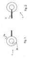
- the bipolar electrodes 1, which are in Fig. 1 can be seen in plan view, consist of an outer ring 2 as an electrode which surrounds the other electrode 2b.
- the inner electrode 2b has its power supply 3 on top of the flexible printed circuit board 10 (FIG. Fig. 3 ). Looking at the electrode from above ( Fig. 2 ), the power supply 3 for the inner electrode can be seen.
- a DC voltage is applied to the inner and outer electrodes. The resulting electrostatic field leads to the attraction of the wafer 5.
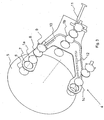
- the electrostatic holder 4 which is in Fig. 3 can be seen in an exploded view, consists of the flexible, printed circuit board 10, on which the conductor tracks 11 for the electrodes 1a-1c are printed.
- the individual layers that make up the gripper, as shown before the assembly.
- the individual layers are (except for the pairs of electrodes) provided only with the upper gripping element with reference numerals.
- the electrodes 1a-1c contain the in Fig. 1 and 2 to be seen bipolar electrode pairs 2a, 2b.
- the conductor tracks 11 each consist of two lines for supplying voltage to the electrodes 1a-1c.
- the above-described layer structure comprising an insulating layer zirconium oxide 6, the bipolar electrode pairs 1a-1c, an insulating layer on the rear side 8 and a base plate 9 for better stability forms an electrostatic gripping element 13a-13c according to the invention.
- the insulating layer is provided in this embodiment with an adhesive film (not shown), whereby the bond improves and air pockets are largely prevented.
- the embodiment has three pairs of electrodes or gripping elements, which are arranged at an angle of 120 ° on a circular path. Thus, the wafer can possibly be caught at the edges.
- the gripping elements 13a-13c consist of the layered structure shown above.
- the aim of the pressing process is to produce a cold weld.
- indium can be used as a network layer (not shown) between the zirconium oxide layer 6 and the electrodes 1a-1c in order to produce an optimum connection between oxide layer and electrodes.
- the power is supplied by the conductor tracks now in the circuit board 11, whose course was determined by the previously provided recesses 12.
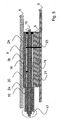
- Fig. 5 shows a sectional view of a gripping element including a captured wafer.
- the wafer 5 below which is the insulating layer of zirconia 6, and then comes the bipolar electrode pair consisting of inner 2b and outer 2a electrode separated by a ring of insulating material 20. Then comes the power supply of the outer electrode 15, which takes place via a conductive layer 19.
- the flexible circuit board 10 made of Kapton.
- the power supply of the inner electrode is made by the conductive layer 18 below and a connection through the circuit board 16, an underlying conductive layer 21 serves as a continuation to other electrodes or gripping elements on the gripper.
- an insulating layer of aluminum (III) oxide 8 below the bottom of a stable base plate 9.
- a channel 13 is still provided for the introduction of insulating material. Such channels serve to introduce insulating material into the channels between the electrodes.
- the lower layer 18 is provided for the inner, the upper layer 19 for the outer electrode.
- the inner electrode has a diameter of 18 mm, the outer an outer diameter of 37 mm.
- Nickel and indium layer are already applied galvanically on the copper electrodes.
- the electrostatic chuck By applying a voltage, the wafer 5 is attracted by electrostatic attraction. Operated at a voltage of 300 V, the electrostatic chuck according to the embodiment achieves a force of 6 N sufficient to lift a wafer.
- the gripper may e.g. be mounted on a robot arm and used for transport, positioning and to bring about any conceivable change in the position of the wafer.
Landscapes
- Engineering & Computer Science (AREA)
- Physics & Mathematics (AREA)
- Condensed Matter Physics & Semiconductors (AREA)
- General Physics & Mathematics (AREA)
- Manufacturing & Machinery (AREA)
- Computer Hardware Design (AREA)
- Microelectronics & Electronic Packaging (AREA)
- Power Engineering (AREA)
- Container, Conveyance, Adherence, Positioning, Of Wafer (AREA)
- Manipulator (AREA)
- Feeding Of Articles By Means Other Than Belts Or Rollers (AREA)
Description
Die Erfindung betrifft einen auf elektrostatischem Prinzip arbeitenden Greifer, insbesondere zur Anwendung in der Halbleiterindustrie.The invention relates to a working on electrostatic principle gripper, in particular for use in the semiconductor industry.
Zum Greifen von Wafern werden zum einen mechanische Greifer eingesetzt. Diese Technik ist vor allem bei kleinen Bauteilen sehr aufwendig und kann zu Beschädigungen und Verunreinigungen des Wafers führen.For gripping wafers on the one hand mechanical grippers are used. This technique is very expensive especially for small components and can lead to damage and contamination of the wafer.
Als Alternative werden Vakuumgreifer eingesetzt, die durch Unterdruck den Wafer ansaugen und so transportieren können. Durch die in der Halbleiterindustrie fortschreitende Verkleinerung der Strukturen wird aber immer mehr in einer Vakuumumgebung produziert. Hier sind Vakuumgreifer naturgemäß nicht einsetzbar.As an alternative, vacuum grippers are used, which can suck in the wafer by vacuum and thus transport it. However, as semiconductor structures continue to shrink in size, more and more is being produced in a vacuum environment. Naturally, vacuum grippers can not be used here.
Andere Greifer arbeiten auf dem Prinzip der elektrostatischen Anziehung.Other grippers work on the principle of electrostatic attraction.
Dabei kann eine Spannung an den Wafer und eine entgegensetzte Spannung an den Greifer gelegt werden. Aufgrund der elektrostatischen Anziehungskraft kann der Wafer dann angehoben und bewegt werden. Nachteilig an diesem Prinzip ist, dass der Wafer zur Anlegung der Spannung elektrisch leitend sein muss. Zum Greifen von nicht leitenden (dielektrischen) Wafern gibt es daher elektrostatische Greifer, die, wie der erfindungsgemäße Greifer, nebeneinander angeordnete Elektroden aufweisen. Auch dieses Prinzip ist schon seit längerem Stand der Technik. So wird z.B. in
Bei herkömmlichen Greifern wird als Isolierschicht meistens Aluminium(III)oxid verwendet (
Um den Wafer zu heben, wird eine entgegengesetzte Spannung an jeweils nebeneinander liegende, entgegengesetzt gepolte Elektroden gelegt. Die Elektroden haben jetzt eine andere Ladung als das zu hebende Bauteil, was zu einer Kraft durch die elektrostatische Anziehung führt. Infolge dieser Kraft bleibt der Wafer am Greifer hängen und kann sodann bewegt werden. Um das Bauteil wieder abzusetzen, werden die Elektroden geerdet.To lift the wafer, an opposite voltage is applied to adjacent, oppositely poled electrodes. The electrodes now have a different charge than the component to be lifted, which leads to a force due to the electrostatic attraction. As a result of this force, the wafer gets stuck on the gripper and can then be moved. To remove the component, the electrodes are grounded.
Ein Nachteil der bekannten Greifer dieses Prinzips ist, dass im Wafer durch die Spannungsdifferenzen ein Strom fließt, der von der Leitfähigkeit des Wafers und der Höhe der Spannung abhängt. Dieser Strom führt zu einer Erwärmung des Wafers, die von dessen Geometrie und Leitfähigkeit, sowie der angelegten Spannung abhängt. Infolge dieser Erwärmung kann es zu Verziehungen und Beschädigungen des Wafers kommen. Dieses Problem besteht infolge der fehlenden Konvektion besonders im Vakuum.A disadvantage of the known grippers of this principle is that in the wafer by the voltage differences, a current flows, which depends on the conductivity of the wafer and the amount of voltage. This current leads to a heating of the wafer, which depends on its geometry and conductivity, as well as the applied voltage. As a result of this heating, warping and damage to the wafer may occur. This problem is due to the lack of convection, especially in a vacuum.
Weiteres Problem beim Einsatz eines elektrostatischen Greifers im Vakuum sind Änderungen in der Überschlagspannung, die zwar sowohl im Hochvakuum, als auch bei Atmosphärendruck über 2000V/mm liegt, bedingt durch die längere mittlere freie Weglänge aber dazwischen bis auf 6V/mm absinkt.Another problem when using an electrostatic Gripper in vacuum are changes in the breakdown voltage, which is both in high vacuum and at atmospheric pressure over 2000V / mm, due to the longer mean free path but in between drops to 6V / mm.
Weiterer Nachteil hoher Spannungen ist, dass durch das damit verbundene hohe Potential die Wafer von angezogenen Staubpartikeln etc. schnell verunreinigt werden. Aufgabe der Erfindung ist es, einen elektrostatischen Greifer zu entwickeln, der die Erwärmung des Wafers auf ein Mindestmaß reduziert und mit möglichst niedriger Spannung betrieben werden kann.Another disadvantage of high voltages is that the wafers are quickly contaminated by attracted dust particles etc. due to the associated high potential. The object of the invention is to develop an electrostatic gripper, which reduces the heating of the wafer to a minimum and can be operated with the lowest possible voltage.
Gelöst wird diese Aufgabe mit einer Greifvorrichtung gemäß den Merkmalen nach Anspruch 1.This object is achieved with a gripping device according to the features of claim 1.
Vorteilhafte und bevorzugte Weiterbildungen sind den jeweils zugeordneten Unteransprüchen zu entnehmen.Advantageous and preferred developments are shown in the respective associated subclaims.
Bei herkömmlichen Greifern wird als Isolierschicht meistens Aluminium(III)oxid verwendet. Nachteilig ist die niedrige relative Dielektizitätskonstante. Mit Zusätzen kann diese verbessert werden (beispielsweise Al 418 der Firma Toto). Nachteilig ist dann aber, dass das Material eine Dicke von etwa 1 mm hat, wodurch zum Erreichen einer gewünschten Dicke von etwa 100 µm aufwendige Schleifarbeiten nötig sind.In conventional grippers is used as an insulating layer mostly aluminum (III) oxide used. A disadvantage is the low relative Dielektizitätskonstante. With additives, this can be improved (for example, Al 418 Toto). However, it is disadvantageous that the material has a thickness of about 1 mm, which requires expensive grinding work to achieve a desired thickness of about 100 μm.
Das beim erfindungsgemäßen Greifer verwendete Zirkoniumoxid, das z.B. zur Produktion von Brennstoffzellen verwendet wird, ist in Schichtdicken von 50-300 µm verfügbar und muss daher nicht oder nur wenig geschliffen werden. Denkbar sind auch Schichtdicken unter 50 µm, die man durch Schleifen oder durch Aufbringen der Zirkoniumoxidschicht in einem CVD- oder sputtering-Verfahren erreicht. Auf letztere Weise sind Schichtdicken im Bereich weniger Atomdurchmesser möglich. Ein weiterer Vorteil ergibt sich aus der höheren Härte des Zirkoniumoxids gegenüber Aluminiumoxid. Sowohl bei der Herstellung, als auch im Betrieb wird die Schicht weniger schnell beschädigt. Die Schicht bleibt zudem glatt, wodurch Beschädigungen des Wafers auch nach längerem Einsatz vermieden werden. Weiterer Vorteil ist der sehr hohe spezifische elektrische Widerstand von ca. 1014 Ωm, weswegen die Schichtdicke sehr klein gehalten werden kann.The zirconium oxide used in the gripper according to the invention, which is used, for example, for the production of fuel cells, is available in layer thicknesses of 50-300 μm and therefore does not need to be sanded or only slightly ground. It is also conceivable layer thicknesses below 50 microns, which can be achieved by grinding or by applying the Zirkoniumoxidschicht in a CVD or sputtering process. In the latter way, layer thicknesses in the range of a few atomic diameter are possible. Another advantage arises from the higher hardness of zirconia over alumina. Both during manufacture and during operation, the layer is damaged less quickly. The layer also remains smooth, which avoids damage to the wafer even after prolonged use. Another advantage is the very high electrical resistivity of about 10 14 Ωm, so the layer thickness can be kept very small.
Infolge der kleinen Schichtdicken und der relativ hohen Dielelektrizitätskonstante kann der erfindungsgemäße Greifer mit einer Gleichspannung von nur 200 bis 900 V betrieben werden, was zu stark reduzierten Strömen im Wafer führt. Bekannte elektrostatische Greifer werden dagegen mit Spannungen zwischen 1 und 6 kV betrieben.Due to the small layer thicknesses and the relatively high dielectric constant, the gripper according to the invention can be operated with a DC voltage of only 200 to 900 V, which leads to greatly reduced currents in the wafer. However, known electrostatic grippers are operated with voltages between 1 and 6 kV.
Der erfindungsgemäße Greifer weist ferner zwei oder mehr Elektrodenpaare auf, die auf einer Schaltplatte aufgebracht sind. So können die Elektrodenpaare an erwärmungs-unempfindlichen Stellen des Wafers angesetzt werden. Die Schaltplatte dient als Halterung der Elektrodenpaare und zugleich ist dort die Spannungsversorgung enthalten.The gripper according to the invention further comprises two or more electrode pairs, which are applied to a circuit board. So the pairs of electrodes can warming-insensitive areas of the wafer are used. The circuit board serves as a holder of the electrode pairs and at the same time there is the power supply included.
Die überwiegend aus Zirkoniumoxid bestehende Schicht des erfindungsgemäßen Greifers kann auch verschiedenste Zusatzstoffe enthalten. So können die mechanischen und elektrischen Eigenschaften geändert werden.The existing predominantly zirconium oxide layer of the gripper invention may also contain a variety of additives. So the mechanical and electrical properties can be changed.
Besonders vorteilhaft hat sich bei einer zweckmäßigen Ausführungsform der Erfindung mit Yttriumoxid stabilisiertes Zirkoniumoxid als Isolationschicht erwiesen. Aber auch eine Isolierschicht aus reinem Zirkoniumoxid ist denkbar.In an advantageous embodiment of the invention, zirconium oxide stabilized with yttrium oxide has proved to be particularly advantageous as an insulating layer. But also an insulating layer of pure zirconium oxide is conceivable.
Eine Weiterbildung der Erfindung hat eine Halterung aus einer flexiblen Schaltplatte. So kann sich der Greifer der Form des Wafers anpassen.A development of the invention has a holder of a flexible circuit board. This allows the gripper to adapt to the shape of the wafer.
Diese Schaltplatte kann zweckmäßigerweise eine gedruckte Schaltplatte sein, die in einem Arbeitsgang kostengünstig herstellbar ist.This circuit board may conveniently be a printed circuit board, which is inexpensive to produce in one operation.
Die Weiterbildung der Erfindung hat Elektrodenpaare, die eine runde, rechteckige oder fingerartige Form haben, und so nur wenig Fläche einnehmen.The development of the invention has electrode pairs, which have a round, rectangular or finger-like shape, and thus take up only a small area.
Diese Elektrodenpaare können so aufgebaut werden, dass der eine Pol vom anderen Pol, z.B. kreisförmig, umschlossen wird.These pairs of electrodes can be constructed so that one pole from the other pole, e.g. circular, is enclosed.
Gegenüber herkömmlichen Bauformen, etwa als nebeneinander angeordnete Leiterbahnen wie in
Zweckmäßigerweise ist der Greifer mit Gleichspannungen unter 900V betreibbar. Durch Reduzierung der Schichtdicken des Zirkoniumoxides und Optimierung der Geometrie sind sogar Spannungen bis unter 300 V denkbar. So ist die Aufheizung des Wafers minimal. Des weiteren werden so Verunreinigungen des Wafers durch angezogene Staubpartikel reduziert und die elektrische Schaltung zum Betrieb des Greifers wird wesentlich einfacher. Auch die Betriebskosten reduzieren sich durch geringeren Stromverbrauch.Conveniently, the gripper with DC voltages operated under 900V. By reducing the layer thicknesses of the zirconium oxide and optimizing the geometry, even voltages below 300 V are conceivable. Thus, the heating of the wafer is minimal. Furthermore, so impurities of the wafer are reduced by attracted dust particles and the electrical circuit for operating the gripper is much easier. The operating costs are also reduced by lower power consumption.
Bei der Weiterbildung der Erfindung kann bei Lösen des Bauteils kurzzeitig eine Wechselspannung angelegt werden. So wird vermieden, dass sich der Wafer wegen eventuell vorhandener elektrostatischer Aufladung nicht löst.In the development of the invention, an alternating voltage can be applied briefly when the component is released. This avoids that the wafer does not dissolve due to the presence of electrostatic charge.
Eine zweckmäßige Ausführungsform hat die Elektrodenpaare im Abstand voneinander so angeordnet, dass der Wafer am Rand gegriffen werden kann. So werden die Vorteile der kompakten Bauform der Elektrodenpaare optimal ausgenutzt. Durch das randseitige Greifen können Erwärmungen in empfindlichen Bereichen des Wafers noch weiter reduziert werden.An expedient embodiment has the electrode pairs spaced apart so that the wafer can be gripped at the edge. Thus, the advantages of the compact design of the electrode pairs are optimally utilized. By gripping on the edge, heating in sensitive areas of the wafer can be further reduced.
Zum Heben hat der Greifer nach einer weiteren Ausführungsform drei auf einer Kreisbahn angeordnete Elektrodenpaare, die idealerweise im 120° -Winkel um den Wafer angeordnet sind. So wird die Gewichtskraft des Wafers an die drei Elektrodenpaare gleich verteilt.For lifting, the gripper according to a further embodiment has three arranged on a circular path electrode pairs, which are ideally arranged at 120 ° angle to the wafer. Thus, the weight of the wafer is distributed equally to the three pairs of electrodes.
Ferner betrifft die Erfindung gemäß Anspruch 12 ein Verfahren zur Herstellung eines elektrostatischen Ein erfindungsgemäßer Greifer kann wie folgt hergestellt werden.Furthermore, the invention according to
Dabei werden Elektrodenpaare auf eine flexible Schaltplatte gebracht. Dann wird eine Vermittlungsschicht auf die Elektroden gebracht. Dazu eignet sich z.B Indium, das in einem galvanischen Prozess in einer Schichtdicke von ca. 10 µm auch schon vorher auf die Elektroden aufgebracht werden kann. Auch eine Schicht Zink kann die Bindung der verschiedenen Materialien verbessern. Die Zirkoniumoxidschicht wird sodann auf die Indiumschicht gebracht. Auf der anderen Seite der Elektrode wird eine Isolierschicht aufgebracht. Dann werden die Schichten zusammengepresst, wodurch sie sich in einem Kaltverschweissungsvorgang miteinander verbinden. Diesem Vorgang kommt eine rauhe Oberfläche einer Zikoniumoxidscheibe zugute.Here, pairs of electrodes are placed on a flexible circuit board. Then it becomes a network layer brought to the electrodes. Indium, for example, which can be applied to the electrodes beforehand in a galvanic process in a layer thickness of approximately 10 μm, is also suitable for this purpose. A layer of zinc can also improve the bonding of the different materials. The zirconium oxide layer is then placed on the indium layer. On the other side of the electrode, an insulating layer is applied. Then the layers are pressed together, joining them together in a cold-welding operation. This process benefits a rough surface of a ziconium oxide disk.
Je nach verwendetem Material für die Isolierschicht kann es, wie in einer Weiterbildung des Verfahrens vorgesehen, zweckmäßig sein, die Isolierschicht aufzukleben, oder eine schon mit Klebemittel beschichtete Isolierschicht zu verwenden.Depending on the material used for the insulating layer may, as provided in a development of the method, be useful to stick the insulating layer, or to use an already coated with adhesive insulating layer.
Als Material für eine solche Isolierschicht eignet sich, wie in einer Ausführungsform des Verfahrens vorgesehen, insbesondere Aluminium(III)oxid. Dieses ist kostengünstig und wird standardmäßig als Isoliermaterial in der Halbleiterindustrie verwendet.As a material for such an insulating layer is, as provided in one embodiment of the method, in particular aluminum (III) oxide. This is inexpensive and is used by default as an insulating material in the semiconductor industry.
Die Elektrodenpaare können zuerst auf eine weitere flexible Schaltplatte aufgebracht werden, z.B. im Ätzverfahren. Die Elektrodenpaare werden dann mit der weiteren Schaltplatte auf die Schaltplatte gebracht. So kann die Herstellung des Greifers zwar nicht in einem Arbeitsgang erfolgen, das Verfahren bietet sich aber dann an, wenn wegen der Geometrie der Elektroden (z.B. sehr klein, Abstand der Elektroden sehr gering) eine Herstellung in einem Schritt technisch nicht machbar oder mit höherem Aufwand verbunden ist.The electrode pairs can first be applied to another flexible circuit board, for example in the etching process. The pairs of electrodes are then placed on the circuit board with the other circuit board. Although the production of the gripper can not be done in one operation, but the process is appropriate if, because of the geometry of the electrodes (eg very small, distance of the electrodes very low) a production in one step technically not feasible or with greater effort connected is.
Im folgenden wird die Erfindung an einem Ausführungsbeispiel anhand der Zeichnungen
- Fig. 1
- zeigt ein Elektrodenpaar in der Draufsicht;
- Fig. 2
- zeigt ein Elektrodenpaar von der Rückseite;
- Fig. 3
- zeigt die einzelnen Bauteile des elektrostatischen Halters in einer Explosionsansicht;
- Fig. 4
- zeigt den fertigen Halter nach dem Pressvorgang;
- Fig. 5
- zeigt eine Schnittansicht eines Greifelementes des Halters.
- Fig. 1
- shows a pair of electrodes in plan view;
- Fig. 2
- shows a pair of electrodes from the back;
- Fig. 3
- shows the individual components of the electrostatic holder in an exploded view;
- Fig. 4
- shows the finished holder after the pressing process;
- Fig. 5
- shows a sectional view of a gripping element of the holder.
Die bipolaren Elektroden 1, die in
Der elektrostatische Halter 4, der in
Vom Wafer 5 beginnend, sieht man davor eine Isolierschicht aus Zirkoniumoxid 6, die Schaltplatte 10, die Elektoden 1a-1c und einer weitere Isolierschicht 8 auf der Rückseite und ferner die Basisplatte 9.Starting from the
Für die Leiterbahnen und die Elektroden nebst Isoliersicht sind in der Schaltplatte 10 Aussparungen 7, 12 vorgesehen. Die Elektroden 1a-1c enthalten die in
Die zuvor beschriebene Schichtstruktur aus einer Isolierschicht Zirkoniumoxid 6, den bipolaren Elektrodenpaaren 1a-1c, einer Isolierschicht auf der Rückseite 8 und einer Basisplatte 9 zur besseren Stabilität bildet ein erfindungsgemäßes elektrostatisches Greifelement 13a-13c.The above-described layer structure comprising an insulating
Die Isolierschicht ist in diesem Ausführungsbeispiel mit einer Klebefolie (nicht dargestellt) versehen, wodurch sich die Bindung verbessert und Lufteinschlüsse weitgehend verhindert werden. Das Ausführungsbeispiel hat drei Elektrodenpaare bzw. Greifelemente, die im Winkel von 120° auf einer Kreisbahn angeordnet sind. So kann der Wafer ggf. an den Rändern gefasst werden.The insulating layer is provided in this embodiment with an adhesive film (not shown), whereby the bond improves and air pockets are largely prevented. The embodiment has three pairs of electrodes or gripping elements, which are arranged at an angle of 120 ° on a circular path. Thus, the wafer can possibly be caught at the edges.
Nach dem Pressvorgang, bei dem der gesamte elektrostatische Greifer mit allen Greifelementen in einem Arbeitsvorgang zusammengefügt werden kann, sind die Schichten miteinander verbunden
Die Schichtdicken und -materialien sind bei diesem Ausführungsbeispiel zwischen der Zirkoniumoxidschicht und der Isolierschicht wie folgt:
- Zwischen 80 und 250
µm Zirkoniumoxid 6. - Ca. 10 µm Indium und 5 µm Nickel als Vermittlungsschicht zwischen Zirkoniumoxidschicht und Kupferelektrode.
- Ca. 17,5 µm Elektroden- und Versorgungsschichten aus
Kupfer 14,15,21. - Ca. 25 µm Schaltplatte aus Kapton oder Polyamid 10.
- Ca. 2,6 mm
Isolierschicht aus Aluminiumoxid 8. - Ca. 0,5 mm Basisplatte aus T 136
NiP 9.
- Between 80 and 250
μm zirconium oxide 6. - Approximately 10 μm indium and 5 μm nickel as a network layer between zirconium oxide layer and copper electrode.
- Approximately 17.5 μm electrode and
supply layers Copper 14,15,21. - Approximately 25 μm PCB made of Kapton or
polyamide 10. - Approximately 2.6 mm insulating layer of
aluminum oxide 8. - Approximately 0.5 mm base plate made of T 136
NiP 9.
Die innere Elektrode hat einen Durchmesser von 18 mm, die äußere einen Außendurchmesser von 37 mm. Nickel und Indiumschicht sind schon vorher auf den Kupferelektroden galvanisch aufgebracht.The inner electrode has a diameter of 18 mm, the outer an outer diameter of 37 mm. Nickel and indium layer are already applied galvanically on the copper electrodes.
Durch Anlegen einer Spannung wird der Wafer 5 durch elektrostatische Anziehung angezogen. Mit einer Spannung von 300 V betrieben, erreicht der elektrostatische Halter gemäß dem Ausführungsbeispiel eine Kraft von 6 N, die ausreichend ist, um einen Wafer anzuheben.By applying a voltage, the
Der Greifer kann z.B. an einen Roboterarm montiert werden und zum Transport, Positionieren und zur Herbeiführung jeder denkbaren Lageänderung des Wafers eingesetzt werden.The gripper may e.g. be mounted on a robot arm and used for transport, positioning and to bring about any conceivable change in the position of the wafer.
Claims (10)
- Gripping device (4) for receiving, holding and/or transporting wafers (5), comprising- a gripping element (13a-13c) disposed on a circuit board (10), wherein the gripping element- contains a bipolar electrode pair (1) to which a voltage can be applied and which consists of an inner (2b) and an outer (2a) electrode which are separated by a ring of insulating material (20), and wherein- at least two gripping elements (1a-1c) are arranged on the circuit board, in which gripping elements the bipolar electrode pairs (1) are provided with an insulating layer (6) which predominantly consists of zirconium oxide,- and wherein the electrode pairs (1a-1c) are mounted in such a spaced relationship that the wafer (5) can be lifted at its edges.
- Gripping device as claimed in claim 1, characterised in that the zirconium oxide is stabilized with yttrium oxide.
- Gripping device as claimed in any one of the preceding claims, characterised in that the holder consists of a flexible circuit board (10).
- Gripping device as claimed in any one of the preceding claims, characterised in that the holder consists of a flexible printed circuit board (10).
- Gripping device as claimed in any one of the preceding claims, characterised in that the electrode pairs (1) are round and/or rectangular and/or finger-like in shape.
- Gripping device as claimed in claim 5, characterised in that in each case one pole (2) surrounds the other pole.
- Gripping device as claimed in any one of the preceding claims, characterised in that the gripper can be operated with a direct voltage of below 900 V and/or 600 V and/or 300 V.
- Gripping device as claimed in any one of the preceding claims, characterised in that when a component is being put down, an alternating voltage can be applied shortly beforehand by grounding.
- Gripping device as claimed in any one of the preceding claims, characterised in that at least three electrode pairs (1a-1c) are disposed on a circular path.
- Gripping device as claimed in claim 9, characterised in that the three electrode pairs (1a-1c) are disposed at approximately a 120° angle around the wafer.
Applications Claiming Priority (2)
| Application Number | Priority Date | Filing Date | Title |
|---|---|---|---|
| DE10232080 | 2002-07-15 | ||
| DE10232080.2A DE10232080B4 (en) | 2002-07-15 | 2002-07-15 | Electrostatic gripper and method for its production |
Publications (3)
| Publication Number | Publication Date |
|---|---|
| EP1387392A2 EP1387392A2 (en) | 2004-02-04 |
| EP1387392A3 EP1387392A3 (en) | 2005-09-07 |
| EP1387392B1 true EP1387392B1 (en) | 2013-04-24 |
Family
ID=30010018
Family Applications (1)
| Application Number | Title | Priority Date | Filing Date |
|---|---|---|---|
| EP03000853.6A Expired - Lifetime EP1387392B1 (en) | 2002-07-15 | 2003-01-15 | Electrostatic gripper |
Country Status (4)
| Country | Link |
|---|---|
| US (1) | US7075772B2 (en) |
| EP (1) | EP1387392B1 (en) |
| JP (1) | JP4159926B2 (en) |
| DE (1) | DE10232080B4 (en) |
Families Citing this family (13)
| Publication number | Priority date | Publication date | Assignee | Title |
|---|---|---|---|---|
| ES2527760T3 (en) * | 1998-07-23 | 2015-01-29 | Yeda Research And Development Co., Ltd. | Treatment of Crohn's disease with copolymer 1 and polypeptides |
| DE10232080B4 (en) * | 2002-07-15 | 2015-10-01 | Integrated Dynamics Engineering Gmbh | Electrostatic gripper and method for its production |
| JP2006026827A (en) * | 2004-07-16 | 2006-02-02 | Aoi Electronics Co Ltd | Nano-gripper device with length measuring function |
| JP4529012B2 (en) * | 2004-07-16 | 2010-08-25 | アオイ電子株式会社 | Nano gripper device |
| WO2011077678A1 (en) * | 2009-12-22 | 2011-06-30 | 株式会社アルバック | Substrate holding apparatus |
| US8672311B2 (en) * | 2010-06-01 | 2014-03-18 | Varian Semiconductor Equipment Associates, Inc. | Method of cooling textured workpieces with an electrostatic chuck |
| DE102010022625A1 (en) | 2010-06-04 | 2011-12-08 | Festo Ag & Co. Kg | Handling system for handling objects |
| DE102010054483A1 (en) * | 2010-12-14 | 2012-06-14 | Manz Automation Ag | Mobile, portable electrostatic substrate holder assembly |
| DE102012019839B4 (en) * | 2012-10-09 | 2017-08-24 | Grenzebach Maschinenbau Gmbh | Method and device for the transport of large-size plates in extreme oversize |
| DE102012019841B4 (en) | 2012-10-09 | 2022-01-05 | Grenzebach Maschinenbau Gmbh | Method and device for moving large, extremely oversized panels |
| DE102012020679B4 (en) * | 2012-10-22 | 2022-01-05 | Grenzebach Maschinenbau Gmbh | Method and device for the rapid relocation of panels |
| EP3375735A1 (en) | 2017-03-17 | 2018-09-19 | Joseph Porat | System and method for automated overhead warehousing |
| KR102334055B1 (en) * | 2019-11-14 | 2021-12-02 | (주)에스티아이 | Loading and unloading robot hand for panel |
Family Cites Families (19)
| Publication number | Priority date | Publication date | Assignee | Title |
|---|---|---|---|---|
| US4184188A (en) * | 1978-01-16 | 1980-01-15 | Veeco Instruments Inc. | Substrate clamping technique in IC fabrication processes |
| JPS57149734A (en) * | 1981-03-12 | 1982-09-16 | Anelva Corp | Plasma applying working device |
| GB2203121A (en) * | 1987-04-06 | 1988-10-12 | Philips Nv | Gripping device |
| US5103367A (en) * | 1987-05-06 | 1992-04-07 | Unisearch Limited | Electrostatic chuck using A.C. field excitation |
| US5822171A (en) * | 1994-02-22 | 1998-10-13 | Applied Materials, Inc. | Electrostatic chuck with improved erosion resistance |
| US5885469B1 (en) * | 1996-11-05 | 2000-08-08 | Applied Materials Inc | Topographical structure of an electrostatic chuck and method of fabricating same |
| JPH07297265A (en) * | 1994-04-26 | 1995-11-10 | Shin Etsu Chem Co Ltd | Electrostatic chuck |
| US5700046A (en) * | 1995-09-13 | 1997-12-23 | Silicon Valley Group, Inc. | Wafer gripper |
| US6354791B1 (en) * | 1997-04-11 | 2002-03-12 | Applied Materials, Inc. | Water lift mechanism with electrostatic pickup and method for transferring a workpiece |
| US6274524B1 (en) * | 1997-04-25 | 2001-08-14 | Kyocera Corporation | Semiconductive zirconia sintering body and electrostatic removing member constructed by semiconductive zirconia sintering body |
| US6075375A (en) * | 1997-06-11 | 2000-06-13 | Applied Materials, Inc. | Apparatus for wafer detection |
| JPH11111828A (en) * | 1997-09-30 | 1999-04-23 | Shin Etsu Chem Co Ltd | Electrostatic sucking device |
| US5880924A (en) * | 1997-12-01 | 1999-03-09 | Applied Materials, Inc. | Electrostatic chuck capable of rapidly dechucking a substrate |
| JPH11168134A (en) * | 1997-12-03 | 1999-06-22 | Shin Etsu Chem Co Ltd | Electrostatic attracting device and manufacture thereof |
| JPH11176920A (en) | 1997-12-12 | 1999-07-02 | Shin Etsu Chem Co Ltd | Electrostatic chuck device |
| JP2000012666A (en) * | 1998-06-19 | 2000-01-14 | Taiheiyo Cement Corp | Electrostatic chuck |
| US6185085B1 (en) * | 1998-12-02 | 2001-02-06 | Taiwan Semiconductor Manufacturing Co., Ltd. | System for transporting and electrostatically chucking a semiconductor wafer or the like |
| KR20020046214A (en) * | 2000-12-11 | 2002-06-20 | 어드밴스드 세라믹스 인터내셔날 코포레이션 | Electrostatic chuck and method of manufacturing the same |
| DE10232080B4 (en) * | 2002-07-15 | 2015-10-01 | Integrated Dynamics Engineering Gmbh | Electrostatic gripper and method for its production |
-
2002
- 2002-07-15 DE DE10232080.2A patent/DE10232080B4/en not_active Expired - Fee Related
-
2003
- 2003-01-15 EP EP03000853.6A patent/EP1387392B1/en not_active Expired - Lifetime
- 2003-05-23 JP JP2003145794A patent/JP4159926B2/en not_active Expired - Fee Related
- 2003-07-05 US US10/613,870 patent/US7075772B2/en not_active Expired - Fee Related
Also Published As
| Publication number | Publication date |
|---|---|
| EP1387392A2 (en) | 2004-02-04 |
| EP1387392A3 (en) | 2005-09-07 |
| JP2004047979A (en) | 2004-02-12 |
| JP4159926B2 (en) | 2008-10-01 |
| DE10232080B4 (en) | 2015-10-01 |
| US20040060172A1 (en) | 2004-04-01 |
| DE10232080A1 (en) | 2004-02-05 |
| US7075772B2 (en) | 2006-07-11 |
Similar Documents
| Publication | Publication Date | Title |
|---|---|---|
| DE60021848T2 (en) | CERAMIC HEATER | |
| EP1387392B1 (en) | Electrostatic gripper | |
| EP0958620B1 (en) | Piezo electric actuator with a new type of contacting and a method for the production thereof | |
| DE112005000621B4 (en) | Bipolar electrostatic holding device | |
| DE10256980B4 (en) | Manufacturing method for a stacked ceramic body | |
| EP0948042A1 (en) | Electrostatic device for clamping wafers and other parts | |
| EP0103748A2 (en) | Combined circuit with varistor | |
| DE102004031404B4 (en) | Piezoelectric component with predetermined breaking point and electrical connection element, method for producing the component and use of the component | |
| DE102004031402A1 (en) | Piezoelectric component with predetermined breaking point, method for producing the component and use of the component | |
| DE102015210736B3 (en) | DEVICE FOR ELECTROSTATIC COUPLING OF A SUBSTRATE WITH A SUBSTRATE CARRIER | |
| DE3145648A1 (en) | SEMICONDUCTOR ARRANGEMENT | |
| WO2010121703A1 (en) | Device and method for separating a substrate from a carrier substrate | |
| DE3143336A1 (en) | SEMICONDUCTOR RECTIFIER UNIT | |
| DE1281601B (en) | Method for producing a magnetic element matrix | |
| EP1473764B1 (en) | Multifunction support for substrat | |
| DE102019211109A1 (en) | Method and cooling body arrangement for cooling semiconductor chips with integrated electronic circuits for power electronic applications | |
| DE4108471A1 (en) | VARISTOR ARRANGEMENTS | |
| DE3322674A1 (en) | CAPACITOR | |
| DE2004776C2 (en) | Semiconductor component | |
| EP1063700A2 (en) | Substrate for high voltage modules | |
| DE1236660B (en) | SEMI-CONDUCTOR ARRANGEMENT WITH A PLATE-SHAPED, BASICALLY SINGLE-CRYSTALLINE SEMICONDUCTOR BODY | |
| DE102004014157B4 (en) | Laminate-type thermistor having a positive temperature coefficient | |
| DE10085266B4 (en) | Electrostatic disk holder | |
| DE102008027115A1 (en) | Contact structure, electronic component with a contact structure and method for its production | |
| DE102007004893B4 (en) | Piezoelectric multilayer actuator and method for its production |
Legal Events
| Date | Code | Title | Description |
|---|---|---|---|
| PUAI | Public reference made under article 153(3) epc to a published international application that has entered the european phase |
Free format text: ORIGINAL CODE: 0009012 |
|
| AK | Designated contracting states |
Kind code of ref document: A2 Designated state(s): AT BE BG CH CY CZ DE DK EE ES FI FR GB GR HU IE IT LI LU MC NL PT SE SI SK TR |
|
| AX | Request for extension of the european patent |
Extension state: AL LT LV MK RO |
|
| PUAL | Search report despatched |
Free format text: ORIGINAL CODE: 0009013 |
|
| AK | Designated contracting states |
Kind code of ref document: A3 Designated state(s): AT BE BG CH CY CZ DE DK EE ES FI FR GB GR HU IE IT LI LU MC NL PT SE SI SK TR |
|
| AX | Request for extension of the european patent |
Extension state: AL LT LV MK RO |
|
| 17P | Request for examination filed |
Effective date: 20060225 |
|
| AKX | Designation fees paid |
Designated state(s): CH DE FR GB LI NL |
|
| REG | Reference to a national code |
Ref country code: DE Ref legal event code: R079 Ref document number: 50314769 Country of ref document: DE Free format text: PREVIOUS MAIN CLASS: H01L0021000000 Ipc: H01L0021683000 |
|
| RIC1 | Information provided on ipc code assigned before grant |
Ipc: H01L 21/683 20060101AFI20121101BHEP |
|
| GRAP | Despatch of communication of intention to grant a patent |
Free format text: ORIGINAL CODE: EPIDOSNIGR1 |
|
| GRAS | Grant fee paid |
Free format text: ORIGINAL CODE: EPIDOSNIGR3 |
|
| GRAA | (expected) grant |
Free format text: ORIGINAL CODE: 0009210 |
|
| AK | Designated contracting states |
Kind code of ref document: B1 Designated state(s): CH DE FR GB LI NL |
|
| RAP1 | Party data changed (applicant data changed or rights of an application transferred) |
Owner name: INTEGRATED DYNAMICS ENGINEERING GMBH |
|
| REG | Reference to a national code |
Ref country code: GB Ref legal event code: FG4D Free format text: NOT ENGLISH |
|
| REG | Reference to a national code |
Ref country code: CH Ref legal event code: NV Representative=s name: BOVARD AG, CH Ref country code: CH Ref legal event code: EP |
|
| REG | Reference to a national code |
Ref country code: DE Ref legal event code: R096 Ref document number: 50314769 Country of ref document: DE Effective date: 20130613 |
|
| REG | Reference to a national code |
Ref country code: NL Ref legal event code: T3 |
|
| PLBE | No opposition filed within time limit |
Free format text: ORIGINAL CODE: 0009261 |
|
| STAA | Information on the status of an ep patent application or granted ep patent |
Free format text: STATUS: NO OPPOSITION FILED WITHIN TIME LIMIT |
|
| 26N | No opposition filed |
Effective date: 20140127 |
|
| REG | Reference to a national code |
Ref country code: DE Ref legal event code: R097 Ref document number: 50314769 Country of ref document: DE Effective date: 20140127 |
|
| REG | Reference to a national code |
Ref country code: FR Ref legal event code: PLFP Year of fee payment: 14 |
|
| REG | Reference to a national code |
Ref country code: FR Ref legal event code: PLFP Year of fee payment: 15 |
|
| PGFP | Annual fee paid to national office [announced via postgrant information from national office to epo] |
Ref country code: NL Payment date: 20170124 Year of fee payment: 15 |
|
| PGFP | Annual fee paid to national office [announced via postgrant information from national office to epo] |
Ref country code: CH Payment date: 20170125 Year of fee payment: 15 Ref country code: FR Payment date: 20170124 Year of fee payment: 15 Ref country code: DE Payment date: 20170128 Year of fee payment: 15 |
|
| PGFP | Annual fee paid to national office [announced via postgrant information from national office to epo] |
Ref country code: GB Payment date: 20170125 Year of fee payment: 15 |
|
| REG | Reference to a national code |
Ref country code: DE Ref legal event code: R119 Ref document number: 50314769 Country of ref document: DE |
|
| REG | Reference to a national code |
Ref country code: CH Ref legal event code: PL |
|
| REG | Reference to a national code |
Ref country code: NL Ref legal event code: MM Effective date: 20180201 |
|
| GBPC | Gb: european patent ceased through non-payment of renewal fee |
Effective date: 20180115 |
|
| PG25 | Lapsed in a contracting state [announced via postgrant information from national office to epo] |
Ref country code: FR Free format text: LAPSE BECAUSE OF NON-PAYMENT OF DUE FEES Effective date: 20180131 Ref country code: DE Free format text: LAPSE BECAUSE OF NON-PAYMENT OF DUE FEES Effective date: 20180801 |
|
| REG | Reference to a national code |
Ref country code: FR Ref legal event code: ST Effective date: 20180928 |
|
| PG25 | Lapsed in a contracting state [announced via postgrant information from national office to epo] |
Ref country code: CH Free format text: LAPSE BECAUSE OF NON-PAYMENT OF DUE FEES Effective date: 20180131 Ref country code: LI Free format text: LAPSE BECAUSE OF NON-PAYMENT OF DUE FEES Effective date: 20180131 Ref country code: NL Free format text: LAPSE BECAUSE OF NON-PAYMENT OF DUE FEES Effective date: 20180201 Ref country code: GB Free format text: LAPSE BECAUSE OF NON-PAYMENT OF DUE FEES Effective date: 20180115 |