EP1382011B1 - Cover incorporating a radio frequency identification device - Google Patents
Cover incorporating a radio frequency identification device Download PDFInfo
- Publication number
- EP1382011B1 EP1382011B1 EP02727693A EP02727693A EP1382011B1 EP 1382011 B1 EP1382011 B1 EP 1382011B1 EP 02727693 A EP02727693 A EP 02727693A EP 02727693 A EP02727693 A EP 02727693A EP 1382011 B1 EP1382011 B1 EP 1382011B1
- Authority
- EP
- European Patent Office
- Prior art keywords
- sheet
- chip
- fact
- thickness
- identification device
- Prior art date
- Legal status (The legal status is an assumption and is not a legal conclusion. Google has not performed a legal analysis and makes no representation as to the accuracy of the status listed.)
- Revoked
Links
Images

Classifications
-
- G—PHYSICS
- G06—COMPUTING; CALCULATING OR COUNTING
- G06K—GRAPHICAL DATA READING; PRESENTATION OF DATA; RECORD CARRIERS; HANDLING RECORD CARRIERS
- G06K19/00—Record carriers for use with machines and with at least a part designed to carry digital markings
- G06K19/06—Record carriers for use with machines and with at least a part designed to carry digital markings characterised by the kind of the digital marking, e.g. shape, nature, code
- G06K19/067—Record carriers with conductive marks, printed circuits or semiconductor circuit elements, e.g. credit or identity cards also with resonating or responding marks without active components
- G06K19/07—Record carriers with conductive marks, printed circuits or semiconductor circuit elements, e.g. credit or identity cards also with resonating or responding marks without active components with integrated circuit chips
- G06K19/077—Constructional details, e.g. mounting of circuits in the carrier
- G06K19/07749—Constructional details, e.g. mounting of circuits in the carrier the record carrier being capable of non-contact communication, e.g. constructional details of the antenna of a non-contact smart card
- G06K19/07758—Constructional details, e.g. mounting of circuits in the carrier the record carrier being capable of non-contact communication, e.g. constructional details of the antenna of a non-contact smart card arrangements for adhering the record carrier to further objects or living beings, functioning as an identification tag
-
- G—PHYSICS
- G06—COMPUTING; CALCULATING OR COUNTING
- G06K—GRAPHICAL DATA READING; PRESENTATION OF DATA; RECORD CARRIERS; HANDLING RECORD CARRIERS
- G06K19/00—Record carriers for use with machines and with at least a part designed to carry digital markings
- G06K19/02—Record carriers for use with machines and with at least a part designed to carry digital markings characterised by the selection of materials, e.g. to avoid wear during transport through the machine
- G06K19/025—Record carriers for use with machines and with at least a part designed to carry digital markings characterised by the selection of materials, e.g. to avoid wear during transport through the machine the material being flexible or adapted for folding, e.g. paper or paper-like materials used in luggage labels, identification tags, forms or identification documents carrying RFIDs
-
- G—PHYSICS
- G06—COMPUTING; CALCULATING OR COUNTING
- G06K—GRAPHICAL DATA READING; PRESENTATION OF DATA; RECORD CARRIERS; HANDLING RECORD CARRIERS
- G06K19/00—Record carriers for use with machines and with at least a part designed to carry digital markings
- G06K19/02—Record carriers for use with machines and with at least a part designed to carry digital markings characterised by the selection of materials, e.g. to avoid wear during transport through the machine
- G06K19/027—Record carriers for use with machines and with at least a part designed to carry digital markings characterised by the selection of materials, e.g. to avoid wear during transport through the machine the material being suitable for use as a textile, e.g. woven-based RFID-like labels designed for attachment to laundry items
-
- G—PHYSICS
- G06—COMPUTING; CALCULATING OR COUNTING
- G06K—GRAPHICAL DATA READING; PRESENTATION OF DATA; RECORD CARRIERS; HANDLING RECORD CARRIERS
- G06K19/00—Record carriers for use with machines and with at least a part designed to carry digital markings
- G06K19/06—Record carriers for use with machines and with at least a part designed to carry digital markings characterised by the kind of the digital marking, e.g. shape, nature, code
- G06K19/067—Record carriers with conductive marks, printed circuits or semiconductor circuit elements, e.g. credit or identity cards also with resonating or responding marks without active components
- G06K19/07—Record carriers with conductive marks, printed circuits or semiconductor circuit elements, e.g. credit or identity cards also with resonating or responding marks without active components with integrated circuit chips
- G06K19/077—Constructional details, e.g. mounting of circuits in the carrier
- G06K19/0772—Physical layout of the record carrier
- G06K19/07728—Physical layout of the record carrier the record carrier comprising means for protection against impact or bending, e.g. protective shells or stress-absorbing layers around the integrated circuit
-
- G—PHYSICS
- G06—COMPUTING; CALCULATING OR COUNTING
- G06K—GRAPHICAL DATA READING; PRESENTATION OF DATA; RECORD CARRIERS; HANDLING RECORD CARRIERS
- G06K19/00—Record carriers for use with machines and with at least a part designed to carry digital markings
- G06K19/06—Record carriers for use with machines and with at least a part designed to carry digital markings characterised by the kind of the digital marking, e.g. shape, nature, code
- G06K19/067—Record carriers with conductive marks, printed circuits or semiconductor circuit elements, e.g. credit or identity cards also with resonating or responding marks without active components
- G06K19/07—Record carriers with conductive marks, printed circuits or semiconductor circuit elements, e.g. credit or identity cards also with resonating or responding marks without active components with integrated circuit chips
- G06K19/077—Constructional details, e.g. mounting of circuits in the carrier
- G06K19/07745—Mounting details of integrated circuit chips
-
- G—PHYSICS
- G06—COMPUTING; CALCULATING OR COUNTING
- G06K—GRAPHICAL DATA READING; PRESENTATION OF DATA; RECORD CARRIERS; HANDLING RECORD CARRIERS
- G06K19/00—Record carriers for use with machines and with at least a part designed to carry digital markings
- G06K19/06—Record carriers for use with machines and with at least a part designed to carry digital markings characterised by the kind of the digital marking, e.g. shape, nature, code
- G06K19/067—Record carriers with conductive marks, printed circuits or semiconductor circuit elements, e.g. credit or identity cards also with resonating or responding marks without active components
- G06K19/07—Record carriers with conductive marks, printed circuits or semiconductor circuit elements, e.g. credit or identity cards also with resonating or responding marks without active components with integrated circuit chips
- G06K19/077—Constructional details, e.g. mounting of circuits in the carrier
- G06K19/07749—Constructional details, e.g. mounting of circuits in the carrier the record carrier being capable of non-contact communication, e.g. constructional details of the antenna of a non-contact smart card
-
- B—PERFORMING OPERATIONS; TRANSPORTING
- B42—BOOKBINDING; ALBUMS; FILES; SPECIAL PRINTED MATTER
- B42D—BOOKS; BOOK COVERS; LOOSE LEAVES; PRINTED MATTER CHARACTERISED BY IDENTIFICATION OR SECURITY FEATURES; PRINTED MATTER OF SPECIAL FORMAT OR STYLE NOT OTHERWISE PROVIDED FOR; DEVICES FOR USE THEREWITH AND NOT OTHERWISE PROVIDED FOR; MOVABLE-STRIP WRITING OR READING APPARATUS
- B42D25/00—Information-bearing cards or sheet-like structures characterised by identification or security features; Manufacture thereof
- B42D25/20—Information-bearing cards or sheet-like structures characterised by identification or security features; Manufacture thereof characterised by a particular use or purpose
- B42D25/24—Passports
-
- H—ELECTRICITY
- H01—ELECTRIC ELEMENTS
- H01L—SEMICONDUCTOR DEVICES NOT COVERED BY CLASS H10
- H01L2924/00—Indexing scheme for arrangements or methods for connecting or disconnecting semiconductor or solid-state bodies as covered by H01L24/00
- H01L2924/0001—Technical content checked by a classifier
- H01L2924/0002—Not covered by any one of groups H01L24/00, H01L24/00 and H01L2224/00
-
- Y—GENERAL TAGGING OF NEW TECHNOLOGICAL DEVELOPMENTS; GENERAL TAGGING OF CROSS-SECTIONAL TECHNOLOGIES SPANNING OVER SEVERAL SECTIONS OF THE IPC; TECHNICAL SUBJECTS COVERED BY FORMER USPC CROSS-REFERENCE ART COLLECTIONS [XRACs] AND DIGESTS
- Y10—TECHNICAL SUBJECTS COVERED BY FORMER USPC
- Y10T—TECHNICAL SUBJECTS COVERED BY FORMER US CLASSIFICATION
- Y10T156/00—Adhesive bonding and miscellaneous chemical manufacture
- Y10T156/10—Methods of surface bonding and/or assembly therefor
- Y10T156/1002—Methods of surface bonding and/or assembly therefor with permanent bending or reshaping or surface deformation of self sustaining lamina
- Y10T156/1039—Surface deformation only of sandwich or lamina [e.g., embossed panels]
Definitions
- the present invention relates to multilayer structures such as booklet covers and their manufacturing processes.
- the covers of the booklets issued by the administrations undergo a very varied mechanical and thermal shock, both during their manufacture and when they are used. These blankets have undergone most often a graining operation intended to give them an attractive surface appearance. During this graining operation, the cover passes between two embossing rollers where it is subjected to a relatively high pressure, of the order of a hundred bars (10 7 Pa).
- cover papers booklets have undergone in some cases also an embellishment operation by application of a "foil” metallized or holographic by a so-called transfer operation hot and under pressure.
- the blanket passes into a press where it is subjected to a relatively high pressure and a relatively high temperature.
- the booklet comprises a notebook consisting of a set of sheets with a cover page which will be laminated on the inside of the front flap of the cover and a transparent film to be transferred hot. on one of the inside pages or on the cover page to protect the variable mentions which have been registered there previously.
- the passport is introduced into a laminator between two heated rollers, and the cover is subjected again to a significant pressure.
- the temperature at which the blanket is exposed can reach 130 ° C for several seconds.
- the passport must also have a life of several years, especially ten years in Europe, and must in particular have the qualities of sufficient resistance to traffic.
- covers for passports are currently manufactured by impregnating with a polymer until saturation a cellulose support of 200 microns thick, then depositing by coating the rake, on one its faces, a covering layer of 50 microns thick, based on polymers and dyes, may comprise expanded microbeads.
- a varnish can then be applied to the layer deposited by coating in order to confer, in particular, gloss on the covering and a certain mechanical resistance to scratch or abrasion.
- radio frequency identification device RFID
- This patent describes a complex that includes a chip. and an antenna, this complex then being inserted for example into the front flap of the passport cover.
- This patent does not discuss in detail how the radio frequency identification device is finally integrated in the passport.
- a first disadvantage of such coverage with radio frequency identification device lies in the lack of homogeneity of the thickness between the front flap and the rear flap of the passport.
- a second drawback arises from the fact that the insertion of the complex into the passport entails an additional processing operation on the passport mounting machine.
- US Patent 5,528,222 discloses an RFID tag.
- the Malaysian passport currently in circulation is equipped with a radio frequency identification device.
- This identification device is inserted into the rear door of the passport when it is mounted, between the grained paper cover and the cover page of the inside pages notebook.
- This radiofrequency identification device is in the form of a trijet complex comprising a chip connected to an antenna, both supported by a polyester film, itself inserted between two other polymer films intended to protect the chip and the antenna. .
- This complex has an extra thickness at the chip.
- the radiofrequency identification device consists simply of a tag (polyester support on which the chip and the antenna are present), for example the Tag device.
- Tag device poly(ethylene support on which the chip and the antenna are present)
- It ® of the company TEXAS INSTRUMENTS is inserted between the grained paper cover and the cover page of the notebook, stuck on the cover.
- the chip causes a local excess thickness of more than 200 microns and its presence can be guessed.
- it remains exposed to shocks and constraints suffered by the passport during the heat transfer of the transparent film, in particular.
- the invention proposes to overcome the drawbacks of the prior art, in particular to provide a booklet cover paper comprising a radio frequency identification device, having no localized excess thickness, and to provide a booklet cover paper comprising a printing device. radio frequency identification ready to be mounted in a passport without additional operation for the transformer.
- the present invention provides a multilayer structure according to claim 1.
- the cover paper must be capable of undergoing graining and / or embellishment treatments by deposition of a film or "foil” by heat transfer and under pressure and / or lamination during the deposition of transparent safety films on the pages containing the variable indications passport.
- the invention makes it possible to obtain a booklet, in particular a passport, whose cover is aesthetic and does not attract the attention of potential falsifiers on the radiofrequency identification device, since it does not have a localized excess thickness and has, where appropriate, appropriate, a grainy appearance.
- the cover paper according to the invention can be used during the manufacture of the passport in the same way as the conventional covering papers not incorporating radiofrequency identification device, which is very advantageous for administrations in particular.
- the chip of the radiofrequency identification device is located near the fold of the cover of the booklet, so as to be in an area less exposed to stress, because partially stiffened by the fold.
- the multilayer structure may comprise at least one sheet having a fibrous base, comprising a greater or lesser amount of natural and / or synthetic fibers, in particular cellulose.
- This fibrous base may contain a polymeric material chosen so as to give the multilayer structure, on the one hand, tear-resistance properties to withstand the subsequent conditions of use and, on the other hand, sufficient resilience properties to protect the radiofrequency identification device for mechanical shocks.
- This material may be chosen for example from the following list: natural or synthetic rubbers, styrene butadiene rubber, polybutadiene, butadiene-acrylonitrile copolymers, acrylic polymers, polychloroprene, and mixtures thereof.
- the chip of the radiofrequency identification device is housed in a layer of the multilayer structure which has a thickness greater than or equal to the thickness of the chip and a resilience enabling it, in case of momentary compression, to conserve a thickness greater than or equal to the thickness of the chip, so as to ensure the protection thereof.
- This layer may comprise a fibrous base comprising a greater or lesser amount of fibers natural and / or synthetic, in particular cellulose, this base itself comprising a polymeric material chosen so as to confer on the multilayer structure the resilience properties sufficient to protect the radiofrequency identification device from mechanical shocks.
- This layer may also be a polymeric base material only, for example a coating based on PVC, possibly plasticized, possibly with blowing agents.
- the multilayer structure may comprise a layer of a polymer-based material capable of graining.
- This polymer can be chosen from the following list: PVC-based polymers, optionally plasticized, of polyurethanes or natural or synthetic elastomers, with possibly blowing agents, emulsions of PVC and butadiene / acrylonitrile copolymer or butadiene copolymer / acrylonitrile / styrene, and mixtures thereof.
- the invention also relates to a passport whose cover is constituted by a multilayer structure as defined above.
- the invention also relates to various methods of manufacturing a cover as defined above.
- the subject of the invention is in particular a method according to claim 18.
- the radiofrequency identification device can be one side of the sheet and then coat this side of the sheet with a mixture based on an ungelled liquid resin, the deposited thickness being greater than that of the chip after drying.
- the layer deposited by coating can be grained after drying.
- a resin based on a hot-melt component it is also possible to deposit on the face of the sheet carrying the radiofrequency identification device a resin based on a hot-melt component, the deposited thickness being greater than the thickness of the chip.
- the coating can be hot-scored to create a grain just before final drying.
- the first sheet may comprise a fibrous base, in particular a paper base, and this fibrous base may be saturated with a material, in particular a polymer, for example an elastomer latex, allowing ensure tear resistance and subsequent protection of the radiofrequency identification device.
- This first sheet may further be coated with a polymer-based mixture, suitable for graining.
- This graft-based polymer-based mixture may alternatively be deposited by coating after assembly of the first and second sheets.
- the second sheet may be impregnated with a thermoplastic polymer.
- a first sheet from a fibrous base preferably saturated with latex
- emboss this first sheet so as to create a cavity having a shape adapted to that of the chip
- second sheet from a fibrous base, preferably saturated by impregnation or mass precipitation with synthetic resins or natural, deposit on this second sheet a chip and an antenna and laminate this second sheet with the first so that the chip come to lodge in the cavity made by the embossing.
- the chip and the antenna may be attached to a support film, for example a polyester film, before being associated with a fibrous base.
- the antenna of the RFID identification device When the antenna of the RFID identification device is made with a conductive ink, it may comprise one or more forging agent, subject of course to compatibility with the ink used.
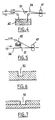
- FIGS. 1 to 3 show a passport 10 whose cover 20 is provided with a radiofrequency identification device 30, comprising a chip 31 and an antenna 32.
- a radiofrequency identification device 30 comprising a chip 31 and an antenna 32.
- the chip incorporates an antenna. This simplifies the incorporation of the radiofrequency identification device into the passport cover but has the disadvantage of reducing the range of the radio link that can be established with a reading device and / or writing.
- the chip 31 is preferably, as can be seen in Figures 1 and 2, near the fold 21 of the cover 20, for example in an area corresponding to a quarter of the width of the front flap 22 or rear 24 of the cover, measured from fold 21.
- the passport 10 comprises a notebook consisting of a set of sheets 11 having a guard page 12 stuck on the back of the front flap 22 of the cover.
- This page 12 is intended to receive an impression of variable mentions then to be covered by a film or "foil" transparent adhesive 13, applied by hot transfer.
- the cover 20 comprises a support layer 24, one face is covered by a layer 25 of a material capable of graining, and the outer surface of the cover 20 has a grain.
- the other face of the support layer 24 carries the chip 31 and its antenna 32 and is covered by a second layer 26, in the thickness of which is housed the chip 31.
- the face 27 of the layer 26, opposite to the layer 24 constitutes the inner surface of the cover 20.
- the antenna 32 When the antenna 32 is made by selective printing of a conductive ink on the layer 24, and has several turns, it may be necessary to locally deposit an insulator 34 on a portion of the turns to be able to carry on this insulation a bridge of electrical connection 35, always by selective deposition of a conductive ink, for connecting one end of the turns to the chip 31.
- the insulator 34 can be deposited, for example, by selective printing.
- the chip 31 can be connected to the antenna 32 according to well known methods, in particular by means of a conductive adhesive, or by thermo-compression or welding.
- the thickness of the layer 26 is greater than the thickness of the chip 31, so that the latter is protected from shocks by both the layer 26 and the layer 24.
- the thickness of the layer 26 is sufficiently large, so that in case of compression of the cover during the embellishment and passport-making processes, the layer 26 retains a thickness greater than that of the chip 31.
- the blanket is capable of undergoing the conventional graining and heat transfer treatments of the film 13 on the cover page 12.
- the cover 20 can be made in many ways, and the layers 24 and 26 can have different constitutions, and include a fibrous base.
- the multilayer structure illustrated in FIG. 3 is in no way limiting of the invention.
- a first sheet with a paper base (fibers of cellulose with or without synthetic fibers), which is saturated with styrene-butadiene copolymer latex to provide tear resistance and subsequent protection of the radiofrequency identification device.
- the chip and the antenna of the radiofrequency identification device are then deposited on one side of this first sheet, after drying, by a conventional method.
- the antenna can be made by screen printing by means of a conductive ink, and then the electrical connections to the chip can be made by thermo-compression.
- an insulator is deposited on part of the turns and an electrical connection bridge is made on this insulator between one end of the turns and the chip.
- the thickness of the first sheet may be of the order of 200 ⁇ m elsewhere, for example.
- FIG. 4 schematically shows the first sheet thus formed, with the chip 31 fixed on it.
- a paper of the blotter type of a thickness greater than that of the chip, is impregnated with a mixture based on polymer (s), for example styrene-butadiene, by passing it through an impregnation bath. to form a second sheet.
- the thickness of this second sheet may be of the order of 300 microns, for example.
- the two sheets are bonded thanks to the mixture of polymer (s) which has been impregnated with blotting paper and the latter matches the relief of the chip because of its compressibility to the wet state.
- the impregnating material is removed and the chip sinks into the blotter-type paper.
- the complex thus formed is then coated on one side, for example the outer face of the first sheet, with a mixture of polymers in order to impart a graining ability.
- the thickness of the layer deposited by coating is for example 50 microns.
- a printing varnish (matt or glossy) can be applied to the layer thus deposited, to improve the surface appearance and the resistance to the circulation.
- a paper of the blotter type of a thickness greater than that of the chip, for example of 300 ⁇ m in thickness, is brought into contact with a gluing machine 42 to impregnate one of its faces with a polymer such as a polyvinyl acetate, then this face thus coated is brought into contact with the first sheet between two rollers 41, as shown in Figure 5.
- the blotting paper saturated with polymer (s) and the first sheet previously manufactured, carrying the radiofrequency identification device on its inner side, bind, blotter-type paper marrying the relief of the chip because of its compressibility in the wet state.
- the complex thus formed is then coated on one of its faces, intended to constitute the outer surface of the cover, with a mixture of polymers having a graining ability.
- the thickness deposited by coating, for example on the outer face of the first sheet, may be of the order of 50 microns.
- a printing varnish (matte or glossy) can be deposited to improve the surface appearance and the resistance to the circulation.
- a first identical sheet is made to that of the previous examples, carrying the radio frequency identification device.
- a second sheet 53 is manufactured with a paper base, shown schematically in FIG. 6, having a hollow watermark 50, in the shape of the chip 31.
- the depth of the watermark 50 is slightly greater than the thickness of the chip 31.
- the thickness of the paper is for example of the order of 300 microns.
- the sheet 53 is preferably saturated with polymer (s) to ensure the subsequent protection of the chip.
- the sheet 53 After marking the locations of the chip 31 and the watermark 50, the sheet 53 is tackled with the first sheet previously made, so that the chip 31 is housed in the watermark 50.
- the bonding can be done cold. or hot. As the sheet 53 is still wet, the complex thus formed is passed between two rolls and proceed to drying.
- the face of the complex intended to constitute the outer surface of the passport may be coated with a mixture of polymers having a graining ability and deposit on this coating a printing varnish (glossy or matte) in order to improve the appearance of the surface and resistance to circulation.
- a printing varnish glossy or matte
- a first identical sheet is made to that of the previous examples, carrying the radio frequency identification device.
- a second sheet is manufactured with a hole made by laser etching or mechanically punch, this hole having a shape corresponding to that of the chip and a thickness at least greater than that of the chip.
- This second sheet may optionally be saturated with polymer (s) to ensure subsequent protection of the chip.
- the second sheet has for example a thickness of the order of 200 microns.
- a third sheet is also produced from a paper base which is preferably saturated with one or more synthetic or natural resins, for example elastomer latexes, by impregnation or precipitation in bulk, the impregnating material. being chosen so as to protect the radiofrequency identification device later.
- This third sheet has for example a thickness of the order of 100 microns.
- the three sheets are laminated spotted, the second sheet being applied to the first sheet having the chip, the latter being housed in the hole.
- the third sheet covers the second sheet on the opposite side to the first.
- the outer face of the first sheet is then coated with a polymer blend having a graining ability.
- a printing varnish gloss or matte
- gloss can be deposited on this coating to improve the surface appearance and the resistance to the circulation.
- a first identical sheet is made to that of the previous examples, carrying the radio frequency identification device.
- This sheet is then coated with a squeegee, on the face comprising the chip, with a "plastisol" type mixture based on PVC added with plasticizer and blowing agent.
- the whole is gelled in a tunnel oven at a temperature of the order of 200 ° C.
- the amounts of plasticizer and blowing agent are adjusted so that the coating has after gelation and cooling compressibility such that the thickness of the layer, during a depression or after a depression, remains greater than thickness of the chip, to protect the latter. For example, a thickness of the order of 300 ⁇ m is deposited.
- the layer deposited by coating can be grained after drying. This layer, after gelation and cooling, provides the desired mechanical characteristics.
- a glossy or matte printing varnish can be deposited on the coating to improve surface appearance and resistance to traffic.
- a sheet identical to the first sheet of the preceding examples is made, bearing the radiofrequency identification device.
- This sheet is then coated on the face carrying the radiofrequency identification device with a mixture based on a so-called "hotmelt” resin , comprising a hot-melt powder, for example polyurethane, using a suitable extrusion system. .
- a hotmelt resin comprising a hot-melt powder, for example polyurethane
- the polymer selected for the coating is chosen so as to have a compressibility such that the thickness of the layer deposited by coating, during a depression or after being seated in the event of impact, remains greater than the thickness of the chip, to protect the latter.
- the deposited thickness is for example of the order of 300 microns.
- the coating produced can be hot-marked to create the desired grain.
- a printing varnish gloss or matte
- a printing varnish can be deposited on the layer deposited by coating, possibly grained, to improve its surface appearance and the resistance to the circulation.
- a first sheet is produced from a paper base (cellulose fibers with or without synthetic fibers), optionally saturated with latex, and a first face of this paper base is coated with a mixture based on polymers exhibiting a graining ability, then possibly a printing varnish (glossy or matte) is deposited on this coating.
- the thickness of the paper base is for example of the order of 200 microns and the thickness of the layer capable of graining of the order of 50 microns.
- a cavity is then produced, at least of greater depth than that of the chip and having a shape adapted to that of the chip, by mechanical embossing on the second face of this paper base.
- the first face is grained simultaneously.
- a second sheet is made, moreover, from a paper base which is preferably saturated by mass impregnation or precipitation with synthetic or natural resins, for example elastomeric latexes, aimed at reinforcing its cohesion and subsequently protecting the device. radio frequency identification.
- the thickness of this second sheet is for example 200 microns.
- This second sheet which carries the chip and the antenna, is then counteracted on the first sheet, so that the chip is housed in the embossed cavity.
- a first sheet is made as in Example 7.
- a cavity of depth substantially equal to half that of the chip on this sheet is then made by mechanical embossing.
- a second sheet is made as in Example 3, with a watermark whose thickness is substantially equal to half that of the chip provided with its antenna, for example the IC-Link ® type of the company INSIDE TECHNOLOGIES.
- the two sheets are then assembled, the chip being completely housed in the cavities facing each of the sheets.
- a first sheet identical to that of the preceding example is produced.
- a conductive ink for example by screen printing, selectively to form two connection areas for the chip and an electrical connection bridge which will subsequently connect a end of the antenna to one of said connection areas.
- An insulating ink is then deposited, for example by screen printing, selectively to form a reserve at the connection areas and at the end of the connecting bridge opposite to the corresponding connection area.
- the turns of the antenna are made by depositing conductive ink, for example by screen printing.
- the ink used may contain tampering agents.
- the antenna is electrically connected at one of its ends to one of the above-mentioned connection areas and at the other end to the free end of the electrical connection bridge.
- Is deposited an insulating layer for example by screen printing, selectively, so as to form a reserve of a thickness at least equivalent to that of the chip and can accommodate it within the final structure without creating extra thickness.
- the thickness of the insulating layer deposited is for example of the order of 300 microns.
- the insulation may be deposited in one or more passes and may include an expansion agent.
- an insulating ink 34 is selectively deposited, and the electrical connection bridge 35 is made between one end of the turns and a connection zone for the chip.
- an insulating layer for example by screen printing, selectively, so as to form a thickness reserve at least equivalent to that of the chip.
- the chip Once the chip is placed in the cavity formed in the insulating layer, it can be covered with an optional protective layer.
- Example 2 The procedure is as in Example 1, with the difference that the chip and the antenna are carried by a thin flexible support such as a synthetic film, a polyester film for example.
- a thin flexible support such as a synthetic film, a polyester film for example.
- the support film, carrying the chip and the antenna, is then associated with a blotter-type sheet.
- the first sheet can be made, alternatively, from the outset with a coating capable of graining and / or receive a printing varnish.
- the material saturating the paper base of the first sheet of Examples 1 to 10 or the second sheet of Examples 1 to 4 may be a natural synthetic resin, for example an elastomer or a mixture of resins. material being selected to provide flexibility, improve tear strength, strain resistance upon compression and resilience. It is especially possible to use as copolymers of elastomer type, copolymers of styrene butadiene (SBR), polybutadiene (BR), butadiene-acrylonitrile copolymers (NBR), acrylic polymers, polychloroprene, polyisoprenes, this list not being limiting.
- SBR styrene butadiene
- BR polybutadiene
- NBR butadiene-acrylonitrile copolymers
- acrylic polymers polychloroprene, polyisoprenes
- polymer (s) used to confer the ability to graining there may be mentioned certain nitro-cellulosic polymers, polyurethanes, acrylic or vinyl.
- thermoplastic polymers based on PVC, polyurethanes and natural or synthetic elastomers.
- plasticized PVC or "plastisol” may be used, which contains plasticizers, for example esters of pthalic acid, odipic acid, sebacic acid or phosphoric acid.
- Polyurethane elastomers can also be used.
- a PVC emulsion can be further blended with other dispersions of butadiene / acrylonitrile copolymers or budatiene / acrylonitrile / styrene copolymer, which act as plasticizers.
- blowing agents functioning for example by an exothermic process.
- blowing agents include products such as azodicarbonanide or azo-sulfohydrazide-based Genitron® which, after decomposition at temperature, give gases such as nitrogen monoxide or hydrogen, carbon dioxide. or ammonia, resulting in the creation of cells and the swelling of the coating.
- water expansion agent in the case of a polyurethane type insulation made from thylene diisocyanate, polyester, and polyether.
- the paper base can be replaced by any other fibrous base, in particular a non-woven fabric.
- the cover may undergo embellishment treatments, in particular the application by heat transfer and under pressure of a colored or holographic metallized film, this film may be deposited on the cover before bonding the notebook or on the booklet after installation of the notebook.
- the cover can receive gravure printing or silk screen printing of a visible or invisible pattern, security or not.
- the cover may comprise a greater or lesser number of different layers.
- the antenna may be made other than by screen printing, for example by transfer of a film covered with copper conductive tracks made by etching.
- the invention is not limited to passports and also applies to the manufacture of family booklets or savings among others.
Abstract
Description
La présente invention concerne des structures multicouches telles que des couvertures de livrets ainsi que leurs procédés de fabrication.The present invention relates to multilayer structures such as booklet covers and their manufacturing processes.
Les papiers couvertures des livrets délivrés par les administrations subissent des chocs mécaniques et thermiques très variés, que ce soit lors de leur fabrication ou lors de leur utilisation. Ces papiers couvertures ont subi le plus souvent une opération de grainage destinée à leur donner un aspect de surface attractif. Lors de cette opération de grainage, la couverture passe entre deux rouleaux d'embossage où elle est soumise à une pression relativement importante, de l'ordre d'une centaine de bars (107 Pa).The covers of the booklets issued by the administrations undergo a very varied mechanical and thermal shock, both during their manufacture and when they are used. These blankets have undergone most often a graining operation intended to give them an attractive surface appearance. During this graining operation, the cover passes between two embossing rollers where it is subjected to a relatively high pressure, of the order of a hundred bars (10 7 Pa).
De plus, ces papiers couvertures des livrets ont subi dans certains cas aussi une opération d'enjolivure par application d'un «foil » métallisé ou holographique par une opération dite de transfert à chaud et sous pression. Lors de cette opération de dépôt de «foil», la couverture passe dans une presse où elle est soumise à une pression relativement importante et à une température relativement élevée.In addition, these cover papers booklets have undergone in some cases also an embellishment operation by application of a "foil" metallized or holographic by a so-called transfer operation hot and under pressure. During this "foil" deposition operation, the blanket passes into a press where it is subjected to a relatively high pressure and a relatively high temperature.
En outre, dans le cas particulier du passeport, le livret comprend un cahier constitué d'un ensemble de feuillets comportant une page de garde qui sera contrecollée sur la face intérieure du volet avant de la couverture et un film transparent destiné à être transféré à chaud sur une des pages intérieures ou sur la page de garde pour protéger les mentions variables qui y ont été inscrites préalablement. Lors de l'opération de transfert, le passeport est introduit dans un laminateur entre deux rouleaux chauffés, et la couverture est soumise une nouvelle fois à une pression non négligeable. La température à laquelle la couverture est exposée peut atteindre 130°C pendant plusieurs secondes.In addition, in the particular case of the passport, the booklet comprises a notebook consisting of a set of sheets with a cover page which will be laminated on the inside of the front flap of the cover and a transparent film to be transferred hot. on one of the inside pages or on the cover page to protect the variable mentions which have been registered there previously. During the transfer operation, the passport is introduced into a laminator between two heated rollers, and the cover is subjected again to a significant pressure. The temperature at which the blanket is exposed can reach 130 ° C for several seconds.
Bien entendu, le passeport doit par ailleurs présenter une durée de vie de plusieurs années, en particulier de dix ans en Europe, et doit notamment posséder les qualités de résistance à la circulation suffisantes.Of course, the passport must also have a life of several years, especially ten years in Europe, and must in particular have the qualities of sufficient resistance to traffic.
Pour répondre aux contraintes mentionnées ci-dessus, certaines couvertures destinées aux passeports sont actuellement fabriquées en imprégnant d'un polymère jusqu'à saturation un support cellulosique de 200 µm d'épaisseur, puis en déposant par enduction à la râcle, sur l'une de ses faces, une couche de recouvrement de 50 µm d'épaisseur, à base de polymères et de colorants, pouvant comporter des micro-billes expansées. Un vernis peut ensuite être appliqué sur la couche déposée par enduction pour conférer notamment de la brillance à la couverture et une certaine résistance mécanique à la rayure ou à l'abrasion.To meet the constraints mentioned above, some covers for passports are currently manufactured by impregnating with a polymer until saturation a cellulose support of 200 microns thick, then depositing by coating the rake, on one its faces, a covering layer of 50 microns thick, based on polymers and dyes, may comprise expanded microbeads. A varnish can then be applied to the layer deposited by coating in order to confer, in particular, gloss on the covering and a certain mechanical resistance to scratch or abrasion.
Par ailleurs, on a cherché à renforcer la sécurité des passeports, notamment en les munissant d'un dispositif d'identification radio-fréquence (RFID), comme décrit dans le brevet US 5 528 222. Ce brevet décrit un complexe qui comprend une puce et une antenne, ce complexe étant ensuite inséré par exemple dans le volet avant de la couverture du passeport. Ce brevet n'aborde toutefois pas de façon détaillée la manière dont le dispositif d'identification radio-fréquence est finalement intégré au passeport. Un premier inconvénient d'une telle couverture avec dispositif d'identification radio fréquence se situe dans l'absence d'homogénéité de l'épaisseur entre le volet avant et le volet arrière du passeport. Un second inconvénient vient du fait que l'insertion du complexe dans le passeport entraîne une opération de transformation supplémentaire sur la machine de montage des passeports.In addition, attempts have been made to strengthen the security of passports, in particular by providing them with a radio frequency identification device (RFID), as described in US Pat. No. 5,528,222. This patent describes a complex that includes a chip. and an antenna, this complex then being inserted for example into the front flap of the passport cover. This patent, however, does not discuss in detail how the radio frequency identification device is finally integrated in the passport. A first disadvantage of such coverage with radio frequency identification device lies in the lack of homogeneity of the thickness between the front flap and the rear flap of the passport. A second drawback arises from the fact that the insertion of the complex into the passport entails an additional processing operation on the passport mounting machine.
La demande internationale WO 00/26856 mentionne également la possibilité de munir un passeport d'un dispositif RFID. La puce est mise en place dans une ouverture d'un film en polyimide ou polyester, et maintenue dans cette ouverture au moyen d'une résine.International application WO 00/26856 also mentions the possibility of providing a passport with an RFID device. The chip is placed in an opening of a polyimide or polyester film, and held in this opening by means of a resin.
La demande internationale WO 00/42569 décrit une étiquette comportant une couche expansible avec une cavité pour recevoir une puce, la cavité étant située au centre de l'étiquette.International application WO 00/42569 discloses a label having an expandable layer with a cavity for receiving a chip, the cavity being located in the center of the label.
Le brevet US 5 528 222 décrit une étiquette RFID.US Patent 5,528,222 discloses an RFID tag.
Le passeport malais actuellement en circulation est muni d'un dispositif d'identification radio-fréquence. Ce dispositif d'identification est inséré dans le volet arrière du passeport lors de son montage, entre le papier couverture grainé et la page de garde du cahier de pages intérieures. Ce dispositif d'identification radiofréquence se présente sous la forme d'un complexe trijet comprenant une puce reliée à une antenne, tous deux supportés par un film polyester, lui-même inséré entre deux autres films polymère destinés à protéger la puce et l'antenne. Ce complexe présente une surépaisseur au niveau de la puce. L'insertion de ce complexe dans le volet arrière du passeport est à l'origine de deux types de surépaisseurs : différence d'épaisseur de 1650 µm entre le volet avant et le volet arrière du passeport, et différence d'épaisseur de 650 µm sur le volet arrière entre la zone où se trouve la puce et la zone où se trouve l'antenne. L'aspect d'un tel passeport attire de plus l'attention des falsificateurs potentiels sur la présence du dispositif RFID.The Malaysian passport currently in circulation is equipped with a radio frequency identification device. This identification device is inserted into the rear door of the passport when it is mounted, between the grained paper cover and the cover page of the inside pages notebook. This radiofrequency identification device is in the form of a trijet complex comprising a chip connected to an antenna, both supported by a polyester film, itself inserted between two other polymer films intended to protect the chip and the antenna. . This complex has an extra thickness at the chip. The insertion of this complex into the rear door of the passport is at the origin of two types of extra thicknesses: difference in thickness of 1650 microns between the front door and the rear door of the passport, and thickness difference of 650 microns on the rear pane between the area where the chip is located and the area where the antenna is located. The appearance of such a passport draws the attention of potential falsifiers to the presence of the RFID device.
Il existe, enfin, des passeports de démonstration dans lesquels le dispositif d'identification radiofréquence constitué simplement d'un tag (support polyester sur lequel sont présents la puce et l'antenne) comme par exemple le dispositif de marque Tag It ® de la société TEXAS INSTRUMENTS, est inséré entre le papier couverture grainé et la page de garde du cahier, collée sur la couverture. La puce entraîne une surépaisseur locale de plus de 200 µm et sa présence se devine. De plus, elle demeure exposée aux chocs et aux contraintes subis par le passeport lors du transfert à chaud du film transparent, notamment.Finally, there are demonstration passports in which the radiofrequency identification device consists simply of a tag (polyester support on which the chip and the antenna are present), for example the Tag device. It ® of the company TEXAS INSTRUMENTS, is inserted between the grained paper cover and the cover page of the notebook, stuck on the cover. The chip causes a local excess thickness of more than 200 microns and its presence can be guessed. In addition, it remains exposed to shocks and constraints suffered by the passport during the heat transfer of the transparent film, in particular.
On connaît par la demande internationale WO 00/42569 une étiquette incorporant un dispositif d'identification radiofréquence. Cette étiquette comporte une couche adhésive et une couche de recouvrement dans l'épaisseur de laquelle est logée la puce du dispositif d'identification radiofréquence. Cette dernière est reliée à une antenne imprimée. Une telle étiquette ne présente pas de surépaisseur au niveau de la puce, mais cependant elle n'est pas adaptée à constituer un dispositif de sécurité satisfaisant pour un passeport, car la présence de l'étiquette sur un des volets de la couverture du passeport entraînerait une différence d'épaisseur entre les deux volets. L'aspect d'un tel passeport attire également l'attention des falsificateurs potentiels sur la présence du dispositif RFID.International application WO 00/42569 discloses a label incorporating a radiofrequency identification device. This label comprises an adhesive layer and a covering layer in the thickness of which is housed the chip of the radiofrequency identification device. The latter is connected to a printed antenna. Such a label does not have any extra thickness at the chip, but however it is not adapted to constitute a satisfactory security device for a passport, because the presence of the label on one of the flaps of the passport cover would cause a difference in thickness between the two shutters. The appearance of such a passport also draws the attention of potential falsifiers to the presence of the RFID device.
L'invention se propose de pallier aux inconvénients de l'art antérieur, notamment de fournir un papier couverture de livret comportant un dispositif d'identification radio fréquence, ne présentant aucune surépaisseur localisée, et de fournir un papier couverture de livret comportant un dispositif d'identification radiofréquence prêt à être monté dans un passeport sans opération supplémentaire pour le transformateur.The invention proposes to overcome the drawbacks of the prior art, in particular to provide a booklet cover paper comprising a radio frequency identification device, having no localized excess thickness, and to provide a booklet cover paper comprising a printing device. radio frequency identification ready to be mounted in a passport without additional operation for the transformer.
Il existe également un besoin pour disposer de livrets, notamment de passeports, qui soient esthétiques et dans lesquels le dispositif d'identification radiofréquence est suffisamment bien protégé pour garantir la fiabilité nécessaire pendant toute la durée de validité du livret, c'est-à-dire plusieurs années dans le cas d'un passeport.There is also a need for books, particularly passports, which are aesthetically pleasing and in which the radiofrequency identification device is sufficiently well protected to ensure the necessary reliability for the duration of validity of the booklet, that is to say say several years in the case of a passport.
La présente invention propose une structure multicouche selon la revendication 1. Notamment, le papier couverture doit être apte à subir les traitements de grainage et/ou d'enjolivure par dépôt d'un film ou « foil » par transfert à chaud et sous pression et/ou de lamination lors de dépôt des films de sécurité transparents sur les pages comportant les mentions variables du passeport.The present invention provides a multilayer structure according to claim 1. In particular, the cover paper must be capable of undergoing graining and / or embellishment treatments by deposition of a film or "foil" by heat transfer and under pressure and / or lamination during the deposition of transparent safety films on the pages containing the variable indications passport.
L'invention permet d'obtenir un livret, notamment de passeport, dont la couverture soit esthétique et n'attire pas l'attention des falsificateurs potentiels sur le dispositif d'identification radiofréquence, car ne présentant pas de surépaisseur localisée et ayant, le cas échéant, un aspect grainé.The invention makes it possible to obtain a booklet, in particular a passport, whose cover is aesthetic and does not attract the attention of potential falsifiers on the radiofrequency identification device, since it does not have a localized excess thickness and has, where appropriate, appropriate, a grainy appearance.
En outre, de par l'absence de surépaisseur localisée et la protection du dispositif d'identification radiofréquence, le papier couverture selon l'invention peut être utilisé lors de la fabrication du passeport de la même manière que les papiers couvertures conventionnels n'incorporant pas de dispositif d'identification radiofréquence, ce qui est très avantageux pour les administrations notamment.In addition, due to the absence of localized excess thickness and the protection of the radiofrequency identification device, the cover paper according to the invention can be used during the manufacture of the passport in the same way as the conventional covering papers not incorporating radiofrequency identification device, which is very advantageous for administrations in particular.
Dans une réalisation particulière, la puce du dispositif d'identification radiofréquence est située à proximité de la pliure de la couverture du livret, de manière à se trouver dans une zone moins exposée aux contraintes, car partiellement rigidifiée par la pliure.In a particular embodiment, the chip of the radiofrequency identification device is located near the fold of the cover of the booklet, so as to be in an area less exposed to stress, because partially stiffened by the fold.
La structure multicouche peut comporter au moins une feuille ayant une base fibreuse, comportant une quantité plus ou moins importante de fibres naturelles et/ou synthétiques, notamment de cellulose. Cette base fibreuse peut contenir un matériau polymère choisi de manière à conférer à la structure multicouche, d'une part des propriétés de résistance à la déchirure pour résister aux conditions d'utilisation ultérieures et d'autre part des propriétés de résilience suffisantes pour protéger le dispositif d'identification radiofréquence des chocs mécaniques. Ce matériau peut être choisi par exemple dans la liste suivante : caoutchoucs naturels ou synthétiques, caoutchouc styrène butadiène, polybutadiène, copolymères butadiène-acrylonitrile, polymères acryliques, polychloroprène, et leurs mélanges.The multilayer structure may comprise at least one sheet having a fibrous base, comprising a greater or lesser amount of natural and / or synthetic fibers, in particular cellulose. This fibrous base may contain a polymeric material chosen so as to give the multilayer structure, on the one hand, tear-resistance properties to withstand the subsequent conditions of use and, on the other hand, sufficient resilience properties to protect the radiofrequency identification device for mechanical shocks. This material may be chosen for example from the following list: natural or synthetic rubbers, styrene butadiene rubber, polybutadiene, butadiene-acrylonitrile copolymers, acrylic polymers, polychloroprene, and mixtures thereof.
Selon l'invention, la puce du dispositif d'identification radiofréquence est logée dans une couche de la structure multicouche qui présente une épaisseur supérieure ou égale à l'épaisseur de la puce et une résilience lui permettant, en cas de compression momentanée, de conserver une épaisseur supérieure ou égale à l'épaisseur de la puce, de manière à assurer la protection de celle-ci. Cette couche peut comporter une base fibreuse comportant une quantité plus ou moins importante de fibres naturelles et/ou synthétiques, notamment de cellulose, cette base comportant elle-même un matériau polymère choisi de manière à conférer à la structure multicouche les propriétés de résilience suffisantes pour protéger le dispositif d'identification radiofréquence des chocs mécaniques. Cette couche peut être aussi un matériau de base polymère uniquement, par exemple une enduction à base de PVC, éventuellement plastifié, avec éventuellement des agents d'expansion.According to the invention, the chip of the radiofrequency identification device is housed in a layer of the multilayer structure which has a thickness greater than or equal to the thickness of the chip and a resilience enabling it, in case of momentary compression, to conserve a thickness greater than or equal to the thickness of the chip, so as to ensure the protection thereof. This layer may comprise a fibrous base comprising a greater or lesser amount of fibers natural and / or synthetic, in particular cellulose, this base itself comprising a polymeric material chosen so as to confer on the multilayer structure the resilience properties sufficient to protect the radiofrequency identification device from mechanical shocks. This layer may also be a polymeric base material only, for example a coating based on PVC, possibly plasticized, possibly with blowing agents.
La structure multicouche peut comporter une couche d'un matériau à base polymère, apte au grainage. Ce polymère peut être choisi dans la liste suivante : polymères à base de PVC, éventuellement plastifié, de polyuréthanes ou d'élastomères naturels ou synthétiques, avec éventuellement des agents d'expansion, émulsions de PVC et de copolymère butadiène/acrylonitrile ou copolymère butadiène/acrylonitrile/styrène, et leurs mélanges.The multilayer structure may comprise a layer of a polymer-based material capable of graining. This polymer can be chosen from the following list: PVC-based polymers, optionally plasticized, of polyurethanes or natural or synthetic elastomers, with possibly blowing agents, emulsions of PVC and butadiene / acrylonitrile copolymer or butadiene copolymer / acrylonitrile / styrene, and mixtures thereof.
L'invention a encore pour objet un passeport dont la couverture est constituée par une structure multicouche telle que définie plus haut.The invention also relates to a passport whose cover is constituted by a multilayer structure as defined above.
L'invention a également pour objet divers procédés de fabrication d'une couverture telle que définie plus haut.The invention also relates to various methods of manufacturing a cover as defined above.
L'invention a notamment pour objet un procédé, selon la revendication 18.The subject of the invention is in particular a method according to claim 18.
On peut par exemple disposer le dispositif d'identification radiofréquence sur une face de la feuille puis enduire cette face de la feuille d'un mélange à base d'une résine liquide non gélifiée, l'épaisseur déposée étant supérieure à celle de la puce après séchage. La couche déposée par enduction peut être grainée après séchage.For example, the radiofrequency identification device can be one side of the sheet and then coat this side of the sheet with a mixture based on an ungelled liquid resin, the deposited thickness being greater than that of the chip after drying. The layer deposited by coating can be grained after drying.
On peut également déposer sur la face de la feuille portant le dispositif d'identification radiofréquence une résine à base d'un composant thermofusible, l'épaisseur déposée étant supérieure à l'épaisseur de la puce. On peut marquer à chaud l'enduction afin de créer un grain juste avant le séchage final.It is also possible to deposit on the face of the sheet carrying the radiofrequency identification device a resin based on a hot-melt component, the deposited thickness being greater than the thickness of the chip. The coating can be hot-scored to create a grain just before final drying.
Dans les exemples de procédés ci-dessus, la première feuille peut comporter une base fibreuse, notamment une base papier, et l'on peut saturer cette base fibreuse avec un matériau, notamment un polymère, par exemple un latex d'élastomère, permettant d'assurer la résistance au déchirement et la protection ultérieure du dispositif d'identification radiofréquence. Cette première feuille peut en outre être enduite par un mélange à base polymère, apte au grainage. Ce mélange à base polymère apte au grainage peut en variante être déposé par enduction après assemblage des première et deuxième feuilles. La deuxième feuille peut être imprégnée avec un polymère thermoplastique.In the examples of the above processes, the first sheet may comprise a fibrous base, in particular a paper base, and this fibrous base may be saturated with a material, in particular a polymer, for example an elastomer latex, allowing ensure tear resistance and subsequent protection of the radiofrequency identification device. This first sheet may further be coated with a polymer-based mixture, suitable for graining. This graft-based polymer-based mixture may alternatively be deposited by coating after assembly of the first and second sheets. The second sheet may be impregnated with a thermoplastic polymer.
On peut encore, selon un autre procédé, réaliser une première feuille à partir d'une base fibreuse, de préférence saturée en latex, embosser cette première feuille de manière à créer une cavité ayant une forme adaptée à celle de la puce, réaliser une deuxième feuille à partir d'une base fibreuse, de préférence saturée par imprégnation ou précipitation en masse avec des résines synthétiques ou naturelles, déposer sur cette deuxième feuille une puce et une antenne et contrecoller cette deuxième feuille avec la première de manière à ce que la puce vienne se loger dans la cavité réalisée par l'embossage.According to another method, it is also possible to produce a first sheet from a fibrous base, preferably saturated with latex, to emboss this first sheet so as to create a cavity having a shape adapted to that of the chip, to make a second sheet from a fibrous base, preferably saturated by impregnation or mass precipitation with synthetic resins or natural, deposit on this second sheet a chip and an antenna and laminate this second sheet with the first so that the chip come to lodge in the cavity made by the embossing.
La puce et l'antenne peuvent être dans un exemple de mise en oeuvre de l'invention fixée sur un film de support, par exemple un film de polyester, avant d'être associées à une base fibreuse.In an exemplary implementation of the invention, the chip and the antenna may be attached to a support film, for example a polyester film, before being associated with a fibrous base.
Lorsque l'antenne du dispositif d'identification RFID est réalisée avec une encre conductrice, celle-ci peut comporter un ou plusieurs agent d'infalsification, sous réserve bien entendu de la compatibilité avec l'encre utilisée.When the antenna of the RFID identification device is made with a conductive ink, it may comprise one or more forging agent, subject of course to compatibility with the ink used.
D'autres caractéristiques et avantages de la présente invention ressortiront à la lecture de la description détaillée qui va suivre, d'exemples de mise en oeuvre non limitatifs, et à l'examen du dessin annexé, sur lequel :
- la figure 1 représente de manière schématique, en perspective, un passeport conforme à l'invention,
- la figure 2 représente le passeport de la figure 1, couverture à plat,
- la figure 3 est une coupe partielle et schématique selon III-III de la figure 2,
- la figure 4 illustre un premier exemple de procédé de fabrication de la couverture,
- la figure 5 illustre un deuxième exemple de procédé de fabrication de la couverture,
- la figure 6 est une coupe partielle et schématique représentant une cavité formée sur l'une des feuilles de la couverture du passeport, et
- la figure 7 est une coupe schématique et partielle d'une cavité réalisée par impression.
- FIG. 1 schematically represents, in perspective, a passport according to the invention,
- FIG. 2 represents the passport of FIG. 1, flat cover,
- FIG. 3 is a partial and schematic section along III-III of FIG. 2,
- FIG. 4 illustrates a first example of a method of manufacturing the cover,
- FIG. 5 illustrates a second example of a method of manufacturing the cover,
- FIG. 6 is a partial schematic section showing a cavity formed on one of the sheets of the passport cover, and
- Figure 7 is a schematic and partial section of a cavity made by printing.
On a représenté sur les figures 1 à 3 un passeport 10 dont la couverture 20 est munie d'un dispositif d'identification radiofréquence 30, comportant une puce 31 et une antenne 32. De nombreux fabricants proposent actuellement des dispositifs d'identification radiofréquence susceptibles de convenir, de sorte que la puce 31 et l'antenne 32 ne seront pas décrites en détail, dans un souci de simplification de l'exposé. On peut citer notamment comme fabricants de puces adaptées, la société INSIDE TECHNOLOGIES, la société TEXAS INSTRUMENTS ou encore la société POLYMERE FLIP CHIP CORPORATION, cette liste n'étant pas limitative.FIGS. 1 to 3 show a
Dans une réalisation non illustrée, la puce intègre une antenne. Cela simplifie l'incorporation du dispositif d'identification radiofréquence dans la couverture du passeport mais présente l'inconvénient de réduire la portée de la liaison radio pouvant être établie avec un dispositif de lecture et/ou d'écriture.In an embodiment not illustrated, the chip incorporates an antenna. This simplifies the incorporation of the radiofrequency identification device into the passport cover but has the disadvantage of reducing the range of the radio link that can be established with a reading device and / or writing.
La puce 31 se situe de préférence, comme on peut le voir sur les figures 1 et 2, à proximité de la pliure 21 de la couverture 20, par exemple dans une zone correspondant à un quart de la largeur du volet avant 22 ou arrière 24 de la couverture, mesurée à partir de la pliure 21.The
Le passeport 10 comporte un cahier constitué d'un ensemble de feuillets 11 ayant une page de garde 12 collée sur le verso du volet avant 22 de la couverture. Cette page de garde 12 est destinée à recevoir une impression de mentions variables puis à être recouverte par un film ou « foil » transparent adhésif 13, appliqué par transfert à chaud.The
Dans l'exemple des figures 1 à 3, la couverture 20 comporte une couche de support 24 dont une face est recouverte par une couche 25 d'un matériau apte au grainage, et la surface extérieure de la couverture 20 présente un grain.In the example of Figures 1 to 3, the
L'autre face de la couche de support 24 porte la puce 31 et son antenne 32 et elle est recouverte par une deuxième couche 26, dans l'épaisseur de laquelle est logée la puce 31. La face 27 de la couche 26, opposée à la couche 24, constitue la surface intérieure de la couverture 20.The other face of the
Lorsque l'antenne 32 est réalisée par impression sélective d'une encre conductrice sur la couche 24, et présente plusieurs spires, il peut être nécessaire de déposer localement un isolant 34 sur une portion des spires afin de pouvoir réaliser sur cet isolant un pont de liaison électrique 35, toujours par dépôt sélectif d'une encre conductrice, pour relier l'une des extrémités des spires à la puce 31. L'isolant 34 peut être déposé, par exemple, par impression sélective. La puce 31 peut être reliée à l'antenne 32 selon des procédés bien connus, notamment par le biais d'une colle conductrice, ou encore par thermo-compression ou par soudure.When the
L'épaisseur de la couche 26 est supérieure à l'épaisseur de la puce 31, de sorte que cette dernière est protégée des chocs à la fois par la couche 26 et par la couche 24.The thickness of the
L'épaisseur de la couche 26 est suffisamment grande, pour qu'en cas de compression de la couverture durant les traitements d'enjolivure et de confection du passeport, la couche 26 conserve une épaisseur supérieure à celle de la puce 31. Ainsi, compte tenu des matériaux utilisés pour réaliser les couches 24 et 26 et des épaisseurs de ces dernières, la couverture est capable de subir les traitements conventionnels de grainage et de transfert à chaud du film 13 sur la page de garde 12.The thickness of the
D'une manière générale, la couverture 20 peut être réalisée de multiples manières, et les couches 24 et 26 peuvent présenter des constitutions différentes, et comportent une base fibreuse. Ainsi, la structure multicouche illustrée à la figure 3 n'est nullement limitative de l'invention.In general, the
On va maintenant donner divers exemples de fabrication de la couverture.We will now give various examples of manufacture of the cover.
On commence par réaliser une première feuille ayant une base papier (fibres de cellulose avec ou sans fibres synthétiques), que l'on sature en latex de copolymère styrène-butadiène pour assurer la résistance au déchirement et la protection ultérieure du dispositif d'identification radiofréquence.We start by making a first sheet with a paper base (fibers of cellulose with or without synthetic fibers), which is saturated with styrene-butadiene copolymer latex to provide tear resistance and subsequent protection of the radiofrequency identification device.
On dépose ensuite sur une face de cette première feuille, après séchage, la puce et l'antenne du dispositif d'identification radiofréquence, par un procédé conventionnel. On peut notamment réaliser l'antenne par sérigraphie au moyen d'une encre conductrice, puis établir les connexions électriques avec la puce par thermo-compression. Le cas échéant, on dépose un isolant sur une partie des spires et l'on réalise sur cet isolant un pont de liaison électrique entre une extrémité des spires et la puce.The chip and the antenna of the radiofrequency identification device are then deposited on one side of this first sheet, after drying, by a conventional method. In particular, the antenna can be made by screen printing by means of a conductive ink, and then the electrical connections to the chip can be made by thermo-compression. Where appropriate, an insulator is deposited on part of the turns and an electrical connection bridge is made on this insulator between one end of the turns and the chip.
A ce stade de la fabrication, sur l'une des faces de la première feuille, il y a une surépaisseur au niveau de l'antenne de l'ordre de 30 µm et au niveau de la puce de l'ordre de 200 µm. L'épaisseur de la première feuille peut être de l'ordre de 200 µm ailleurs, par exemple.At this stage of manufacture, on one of the faces of the first sheet, there is an extra thickness at the antenna of the order of 30 microns and at the chip of the order of 200 microns. The thickness of the first sheet may be of the order of 200 μm elsewhere, for example.
On a représenté sur la figure 4, schématiquement, la première feuille ainsi formée, avec la puce 31 fixée dessus.FIG. 4 schematically shows the first sheet thus formed, with the
Par ailleurs, on imprègne avec un mélange à base de polymère(s), par exemple de styrène-butadiène, un papier de type buvard, d'épaisseur supérieure à celle de la puce, en le faisant passer dans un bain d'imprégnation 40 pour former une deuxième feuille. L'épaisseur de cette deuxième feuille peut être de l'ordre de 300 µm, par exemple.On the other hand, a paper of the blotter type, of a thickness greater than that of the chip, is impregnated with a mixture based on polymer (s), for example styrene-butadiene, by passing it through an impregnation bath. to form a second sheet. The thickness of this second sheet may be of the order of 300 microns, for example.
Ensuite, on fait passer entre deux rouleaux 41 le papier de type buvard, humide saturé en polymère(s) et la première feuille préalablement fabriquée, avec le dispositif d'identification radiofréquence sur sa face intérieure.Next, two saturated wet-saturated paper of the polymer (s) type and the first previously manufactured sheet are passed between two
Lors de l'opération d'essorage, les deux feuilles se lient grâce au mélange à base de polymère(s) dont a été imprégné le papier de type buvard et ce dernier épouse le relief de la puce du fait de sa compressibilité à l'état humide. Ainsi, à l'emplacement de la puce, sous l'effet de la pression des rouleaux 41, le matériau d'imprégnation est chassé et la puce s'enfonce dans le papier de type buvard.During the spinning operation, the two sheets are bonded thanks to the mixture of polymer (s) which has been impregnated with blotting paper and the latter matches the relief of the chip because of its compressibility to the wet state. Thus, at the location of the chip, under the effect of the pressure of the
On enduit ensuite le complexe ainsi formé, sur une face, par exemple la face extérieure de la première feuille, avec un mélange de polymères, afin de conférer une aptitude au grainage. L'épaisseur de la couche déposée par enduction est par exemple de 50 µm.The complex thus formed is then coated on one side, for example the outer face of the first sheet, with a mixture of polymers in order to impart a graining ability. The thickness of the layer deposited by coating is for example 50 microns.
Un vernis d'impression (mat ou brillant) peut être appliqué sur la couche ainsi déposée, pour améliorer l'aspect de surface et la résistance à la circulation.A printing varnish (matt or glossy) can be applied to the layer thus deposited, to improve the surface appearance and the resistance to the circulation.
Dans ce deuxième exemple, on réalise une première feuille identique à celle de l'exemple précédent, portant le dispositif d'identification radiofréquence.In this second example, a first identical sheet is made to that of the previous example, carrying the radiofrequency identification device.
On amène un papier de type buvard, d'épaisseur supérieure à celle de la puce, par exemple de 300 µm d'épaisseur, au contact d'une encolleuse 42 pour imprégner l'une de ses faces d'un polymère tel qu'un polyacétate de vinyle, puis cette face ainsi enduite est amenée au contact de la première feuille, entre deux rouleaux 41, comme illustré à la figure 5.A paper of the blotter type, of a thickness greater than that of the chip, for example of 300 μm in thickness, is brought into contact with a gluing
Le papier de type buvard, saturé en polymère(s) et la première feuille préalablement fabriquée, portant le dispositif d'identification radiofréquence sur sa face intérieure, se lient, le papier de type buvard épousant le relief de la puce du fait de sa compressibilité à l'état humide.The blotting paper, saturated with polymer (s) and the first sheet previously manufactured, carrying the radiofrequency identification device on its inner side, bind, blotter-type paper marrying the relief of the chip because of its compressibility in the wet state.
On enduit ensuite le complexe ainsi formé sur l'une de ses faces, destinée à constituer la surface extérieure de la couverture, avec un mélange de polymères présentant une aptitude au grainage. L'épaisseur déposée par enduction, par exemple sur la face extérieure de la première feuille, peut être de l'ordre de 50 µm.The complex thus formed is then coated on one of its faces, intended to constitute the outer surface of the cover, with a mixture of polymers having a graining ability. The thickness deposited by coating, for example on the outer face of the first sheet, may be of the order of 50 microns.
Comme dans l'exemple précédent, un vernis d'impression (mat ou brillant) peut être déposé pour améliorer l'aspect de surface et la résistance à la circulation.As in the previous example, a printing varnish (matte or glossy) can be deposited to improve the surface appearance and the resistance to the circulation.
On réalise une première feuille identique à celle des exemples précédents, portant le dispositif d'identification radiofréquence.A first identical sheet is made to that of the previous examples, carrying the radio frequency identification device.
On fabrique une deuxième feuille 53 avec une base papier, représentée schématiquement à la figure 6, présentant un filigrane 50 en creux, de la forme de la puce 31. La profondeur du filigrane 50 est légèrement supérieure à l'épaisseur de la puce 31. L'épaisseur du papier est par exemple de l'ordre de 300 µm. La feuille 53 est de préférence saturée en polymère(s) pour assurer la protection ultérieure de la puce.A second sheet 53 is manufactured with a paper base, shown schematically in FIG. 6, having a
On contrecolle, après avoir repéré les emplacements de la puce 31 et du filigrane 50, la feuille 53 avec la première feuille précédemment réalisée, de manière à ce que la puce 31 vienne se loger dans le filigrane 50. Le collage peut se faire à froid ou à chaud. La feuille 53 étant encore humide, on passe le complexe ainsi formé entre deux rouleaux et l'on procède à son séchage.After marking the locations of the
On peut enduire la face du complexe destinée à constituer la surface extérieure du passeport avec un mélange de polymères présentant une aptitude au grainage et déposer sur cette enduction un vernis d'impression (brillant ou mat) afin d'améliorer l'aspect de surface et la résistance à la circulation.The face of the complex intended to constitute the outer surface of the passport may be coated with a mixture of polymers having a graining ability and deposit on this coating a printing varnish (glossy or matte) in order to improve the appearance of the surface and resistance to circulation.
On réalise une première feuille identique à celle des exemples précédents, portant le dispositif d'identification radiofréquence.A first identical sheet is made to that of the previous examples, carrying the radio frequency identification device.
Une deuxième feuille est fabriquée avec un trou réalisé par gravure laser ou mécaniquement à l'emporte pièce, ce trou ayant une forme correspondant à celle de la puce et une épaisseur au moins supérieure à celle de la puce. Cette deuxième feuille peut éventuellement être saturée en polymère(s) pour assurer une protection ultérieure de la puce. La deuxième feuille présente par exemple une épaisseur de l'ordre de 200 µm.A second sheet is manufactured with a hole made by laser etching or mechanically punch, this hole having a shape corresponding to that of the chip and a thickness at least greater than that of the chip. This second sheet may optionally be saturated with polymer (s) to ensure subsequent protection of the chip. The second sheet has for example a thickness of the order of 200 microns.
On fabrique par ailleurs une troisième feuille, à partir d'une base papier, que l'on sature de préférence avec une ou plusieurs résines synthétiques ou naturelles, par exemple des latex élastomères, par imprégnation ou précipitation en masse, le matériau d'imprégnation étant choisi de manière à protéger le dispositif d'identification radiofréquence ultérieurement. Cette troisième feuille présente par exemple une épaisseur de l'ordre de 100 µm.A third sheet is also produced from a paper base which is preferably saturated with one or more synthetic or natural resins, for example elastomer latexes, by impregnation or precipitation in bulk, the impregnating material. being chosen so as to protect the radiofrequency identification device later. This third sheet has for example a thickness of the order of 100 microns.
Ensuite, les trois feuilles sont contrecollées de manière repérée, la deuxième feuille étant appliquée sur la première feuille comportant la puce, cette dernière venant se loger dans le trou. La troisième feuille vient recouvrir la deuxième feuille du côté opposé à la première.Then, the three sheets are laminated spotted, the second sheet being applied to the first sheet having the chip, the latter being housed in the hole. The third sheet covers the second sheet on the opposite side to the first.
On enduit ensuite la face extérieure de la première feuille avec un mélange de polymères présentant une aptitude au grainage.The outer face of the first sheet is then coated with a polymer blend having a graining ability.
Eventuellement, un vernis d'impression (brillant ou mat) peut être déposé sur cette enduction pour améliorer l'aspect de surface et la résistance à la circulation.Optionally, a printing varnish (glossy or matte) can be deposited on this coating to improve the surface appearance and the resistance to the circulation.
On réalise une première feuille identique à celle des exemples précédents, portant le dispositif d'identification radiofréquence.A first identical sheet is made to that of the previous examples, carrying the radio frequency identification device.
On enduit ensuite cette feuille à l'aide d'un racle, sur la face comportant la puce, avec un mélange type « plastisol » à base de PVC additionné de plastifiant et d'agent gonflant. On gélifie l'ensemble dans un four à tunnel à la température de l'ordre de 200°C. Les quantités de plastifiant et d'agent gonflant sont ajustées de façon à ce que l'enduction présente après gélification et refroidissement une compressibilité telle que l'épaisseur de la couche, lors d'un enfoncement ou après un enfoncement, reste supérieure à l'épaisseur de la puce, afin de protéger cette dernière. On dépose par exemple une épaisseur de l'ordre de 300 µm. La couche déposée par enduction peut être grainée après séchage. Cette couche, après gélification et refroidissement, apporte les caractéristiques mécaniques recherchées.This sheet is then coated with a squeegee, on the face comprising the chip, with a "plastisol" type mixture based on PVC added with plasticizer and blowing agent. The whole is gelled in a tunnel oven at a temperature of the order of 200 ° C. The amounts of plasticizer and blowing agent are adjusted so that the coating has after gelation and cooling compressibility such that the thickness of the layer, during a depression or after a depression, remains greater than thickness of the chip, to protect the latter. For example, a thickness of the order of 300 μm is deposited. The layer deposited by coating can be grained after drying. This layer, after gelation and cooling, provides the desired mechanical characteristics.
Un vernis d'impression (brillant ou mat) peut être déposé sur l'enduction pour améliorer l'aspect de surface et la résistance à la circulation.A glossy or matte printing varnish can be deposited on the coating to improve surface appearance and resistance to traffic.
On réalise une feuille identique à la première feuille des exemples précédents, portant le dispositif d'identification radiofréquence.A sheet identical to the first sheet of the preceding examples is made, bearing the radiofrequency identification device.
On enduit ensuite cette feuille sur la face portant le dispositif d'identification radiofréquence avec un mélange à base d'une résine dite « hotmelt », comprenant une poudre thermofusible, par exemple du polyuréthane à l'aide d'un système d'extrusion adapté.This sheet is then coated on the face carrying the radiofrequency identification device with a mixture based on a so-called "hotmelt" resin , comprising a hot-melt powder, for example polyurethane, using a suitable extrusion system. .
Le polymère retenu pour l'enduction est choisi de manière à présenter une compressibilité telle que l'épaisseur de la couche déposée par enduction, lors d'un enfoncement ou après enfoncement en cas de choc, reste supérieure à l'épaisseur de la puce, afin de protéger cette dernière. L'épaisseur déposée est par exemple de l'ordre de 300 µm.The polymer selected for the coating is chosen so as to have a compressibility such that the thickness of the layer deposited by coating, during a depression or after being seated in the event of impact, remains greater than the thickness of the chip, to protect the latter. The deposited thickness is for example of the order of 300 microns.
On peut marquer à chaud l'enduction réalisée afin de créer le grain souhaité.The coating produced can be hot-marked to create the desired grain.
Ensuite, un vernis d'impression (brillant ou mat) peut être déposé sur la couche déposée par enduction, éventuellement grainée, pour améliorer son aspect de surface et la résistance à la circulation.Then, a printing varnish (glossy or matte) can be deposited on the layer deposited by coating, possibly grained, to improve its surface appearance and the resistance to the circulation.
On réalise une première feuille à partir d'une base papier (fibres de cellulose avec ou sans fibres synthétiques), éventuellement saturée en latex, et l'on enduit une première face de cette base papier d'un mélange à base de polymères présentant une aptitude au grainage, puis on dépose éventuellement un vernis d'impression (brillant ou mat) sur cette enduction. L'épaisseur de la base papier est par exemple de l'ordre de 200 µm et l'épaisseur de la couche apte au grainage de l'ordre de 50 µm.A first sheet is produced from a paper base (cellulose fibers with or without synthetic fibers), optionally saturated with latex, and a first face of this paper base is coated with a mixture based on polymers exhibiting a graining ability, then possibly a printing varnish (glossy or matte) is deposited on this coating. The thickness of the paper base is for example of the order of 200 microns and the thickness of the layer capable of graining of the order of 50 microns.
On réalise ensuite une cavité, de profondeur au moins supérieure à celle de la puce et ayant une forme adaptée à celle de la puce, par embossage mécanique sur la deuxième face de cette base papier.A cavity is then produced, at least of greater depth than that of the chip and having a shape adapted to that of the chip, by mechanical embossing on the second face of this paper base.
Eventuellement, la première face est grainée simultanément.Optionally, the first face is grained simultaneously.
Une seconde feuille est fabriquée par ailleurs, à partir d'une base papier qui est de préférence saturée par imprégnation ou précipitation en masse avec des résines synthétiques ou naturelles, par exemple des latex élastomères, visant à renforcer sa cohésion et à protéger ultérieurement le dispositif d'identification radiofréquence. L'épaisseur de cette seconde feuille est par exemple de 200 µm.A second sheet is made, moreover, from a paper base which is preferably saturated by mass impregnation or precipitation with synthetic or natural resins, for example elastomeric latexes, aimed at reinforcing its cohesion and subsequently protecting the device. radio frequency identification. The thickness of this second sheet is for example 200 microns.
Sur cette seconde feuille, on dépose une puce et une antenne par un procédé conventionnel.On this second sheet, a chip and an antenna are deposited by a conventional method.
On contrecolle ensuite cette seconde feuille, portant la puce et l'antenne, sur la première feuille, de manière à ce que la puce vienne se loger dans la cavité réalisée par embossage.This second sheet, which carries the chip and the antenna, is then counteracted on the first sheet, so that the chip is housed in the embossed cavity.
Après contrecollage, le complexe formé est séché.After lamination, the complex formed is dried.
On réalise une première feuille comme dans l'exemple 7.A first sheet is made as in Example 7.
On réalise ensuite une cavité de profondeur sensiblement égale à la moitié de celle de la puce sur cette feuille, par embossage mécanique.A cavity of depth substantially equal to half that of the chip on this sheet is then made by mechanical embossing.
On réalise une deuxième feuille comme dans l'exemple 3, avec un filigrane dont l'épaisseur est sensiblement égale à la moitié de celle de la puce munie de son antenne, par exemple du type IC-Link ® de la société INSIDE TECHNOLOGIES.A second sheet is made as in Example 3, with a watermark whose thickness is substantially equal to half that of the chip provided with its antenna, for example the IC-Link ® type of the company INSIDE TECHNOLOGIES.
On assemble ensuite les deux feuilles, la puce étant complètement logée dans les cavités en regard de chacune des feuilles.The two sheets are then assembled, the chip being completely housed in the cavities facing each of the sheets.
On réalise une première feuille identique à celle de l'exemple précédent.A first sheet identical to that of the preceding example is produced.
On munit ensuite la face de cette première feuille opposée à celle portant l'enduction du dispositif d'identification radiofréquence.The face of this first sheet opposite to that bearing the coating of the radiofrequency identification device is then provided.
Pour ce faire, on peut commencer par déposer une encre conductrice, par exemple par sérigraphie, de façon sélective afin de former deux zones de connexion pour la puce et un pont de liaison électrique qui permettra de relier ultérieurement une extrémité de l'antenne à l'une desdites zones de connexion.To do this, we can begin by depositing a conductive ink, for example by screen printing, selectively to form two connection areas for the chip and an electrical connection bridge which will subsequently connect a end of the antenna to one of said connection areas.
On dépose ensuite une encre isolante, par exemple par sérigraphie, de façon sélective, afin de former une réserve au niveau des zones de connexion et au niveau de l'extrémité du pont de liaison opposée à la zone de connexion correspondante.An insulating ink is then deposited, for example by screen printing, selectively to form a reserve at the connection areas and at the end of the connecting bridge opposite to the corresponding connection area.
On réalise les spires de l'antenne en déposant de l'encre conductrice, par exemple par sérigraphie. L'encre utilisée peut contenir des agents d'infalsification. L'antenne est connectée électriquement par l'une de ses extrémités à l'une des zones de connexion précitées et par l'autre extrémité à l'extrémité libre du pont de liaison électrique.The turns of the antenna are made by depositing conductive ink, for example by screen printing. The ink used may contain tampering agents. The antenna is electrically connected at one of its ends to one of the above-mentioned connection areas and at the other end to the free end of the electrical connection bridge.
On dépose une couche isolante, par exemple par sérigraphie, de façon sélective, de façon à former une réserve d'une épaisseur au moins équivalente à celle de la puce et pouvoir loger celle-ci au sein de la structure finale sans créer de surépaisseur. L'épaisseur de la couche d'isolant déposée est par exemple de l'ordre de 300 µm. L'isolant peut être déposé en une ou plusieurs passes et peut comporter un agent d'expansion.Is deposited an insulating layer, for example by screen printing, selectively, so as to form a reserve of a thickness at least equivalent to that of the chip and can accommodate it within the final structure without creating extra thickness. The thickness of the insulating layer deposited is for example of the order of 300 microns. The insulation may be deposited in one or more passes and may include an expansion agent.
Après mise en place de la puce on procède, éventuellement, au dépôt d'une couche de protection facultative sur la couche d'isolant.After placement of the chip is proceeded, optionally, depositing an optional protective layer on the insulating layer.
On commence par réaliser une première feuille identique à celle de l'exemple précédent.We begin by making a first sheet identical to that of the previous example.
Ensuite, on dépose par exemple par sérigraphie sur la face de cette première feuille opposée à celle qui a été enduite d'un mélange apte au grainage, une encre conductrice de manière à former les spires de l'antenne.Then, for example by screen printing on the face of this first sheet opposite to that which has been coated with a mixture suitable for graining, a conductive ink so as to form the turns of the antenna.
Après, on dépose de manière sélective une encre isolante 34, et l'on réalise le pont de liaison électrique 35 entre une extrémité des spires et une zone de connexion pour la puce. On procède alors au dépôt d'une couche isolante, par exemple par sérigraphie, de façon sélective, afin de former une réserve d'épaisseur au moins équivalente à celle de la puce.After that, an insulating
Une fois la puce mise en place dans la cavité formée dans la couche isolante, on peut recouvrir celle-ci d'une couche de protection facultative.Once the chip is placed in the cavity formed in the insulating layer, it can be covered with an optional protective layer.
On procède comme dans l'exemple 1, à la différence près que la puce et l'antenne sont portées par un support flexible de faible épaisseur tel qu'un film synthétique, un film de polyester par exemple.The procedure is as in Example 1, with the difference that the chip and the antenna are carried by a thin flexible support such as a synthetic film, a polyester film for example.
Le film de support, portant la puce et l'antenne, est ensuite associé à une feuille de type buvard.The support film, carrying the chip and the antenna, is then associated with a blotter-type sheet.
Dans les exemples 1 à 6, la première feuille peut être réalisée, en variante, dès l'origine avec une enduction apte au grainage et/ou recevoir un vernis d'impression.In Examples 1 to 6, the first sheet can be made, alternatively, from the outset with a coating capable of graining and / or receive a printing varnish.
D'une manière générale, le matériau saturant la base papier de la première feuille des exemples 1 à 10 ou la deuxième feuille des exemples 1 à 4, peut être une résine synthétique, naturelle, par exemple un élastomère ou un mélange de résines, ce matériau étant choisi afin d'apporter de la flexibilité, améliorer la résistance à la déchirure, la résistance à la déformation lors d'une compression et la résilience. On peut notamment utiliser comme polymère de type élastomère, des copolymères de styrène butadiène (SBR), du polybutadiène (BR), des copolymères butadiène-acrylonitrile (NBR), des polymères acryliques, du polychloroprène, des polyisoprènes, cette liste n'étant pas limitative.In general, the material saturating the paper base of the first sheet of Examples 1 to 10 or the second sheet of Examples 1 to 4 may be a natural synthetic resin, for example an elastomer or a mixture of resins. material being selected to provide flexibility, improve tear strength, strain resistance upon compression and resilience. It is especially possible to use as copolymers of elastomer type, copolymers of styrene butadiene (SBR), polybutadiene (BR), butadiene-acrylonitrile copolymers (NBR), acrylic polymers, polychloroprene, polyisoprenes, this list not being limiting.
Comme mélange à base de polymère(s) utilisable pour conférer l'aptitude au grainage, on peut citer certains polymères nitro cellulosiques, polyurethanes, acryliques ou vinyliques.As the mixture based on polymer (s) used to confer the ability to graining, there may be mentioned certain nitro-cellulosic polymers, polyurethanes, acrylic or vinyl.
Comme polymères utilisable(s) pour constituer l'isolant des exemples 5 et 6, on peut citer les polymères thermoplastiques à base de PVC, de polyuréthanes et les élastomères naturels ou synthétiques. On peut notamment utiliser du PVC plastifié ou « plastisol », qui contient des plastifiants, par exemple des esters de l'acide pthalique, de l'acide odipique, de l'acide sébacique ou de l'acide phosphorique. On peut aussi utiliser des élastomères de polyuréthane. On peut encore mélanger une émulsion de PVC avec d'autres dispersions de copolymères butadiène/acrylonitrile ou copolymère budatiène/acrylonitrile/styrène, qui jouent le rôle d'agents plastifiants. On peut enfin introduire dans le polymère, notamment lorsque celui-ci est déposé par impression ou enduction, et comporte par exemple du PVC, des agents d'expansion fonctionnant par exemple par un procédé exothermique. Comme agents d'expansion, on peut citer notamment des produits comme le Génitron® à base d'azodicarbonanide ou de sulfohydrazide, qui après décomposition à la température donne des gaz tels que le monoxyde d'azote ou l'hydrogène, le dioxyde de carbone ou l'ammoniac, entraînant ainsi la création de cellules et le gonflement de l'enduction. On peut aussi utiliser comme agent d'expansion de l'eau, dans le cas d'un isolant de type polyuréthane fabriqué à partir de disocyanate de thylène, de polyester, et de polyether.As polymers usable (s) to form the insulator of Examples 5 and 6, mention may be made of thermoplastic polymers based on PVC, polyurethanes and natural or synthetic elastomers. In particular, plasticized PVC or "plastisol" may be used, which contains plasticizers, for example esters of pthalic acid, odipic acid, sebacic acid or phosphoric acid. Polyurethane elastomers can also be used. A PVC emulsion can be further blended with other dispersions of butadiene / acrylonitrile copolymers or budatiene / acrylonitrile / styrene copolymer, which act as plasticizers. Finally, it is possible to introduce into the polymer, especially when the latter is deposited by printing or coating, and for example comprises PVC, blowing agents functioning for example by an exothermic process. Examples of blowing agents that may be mentioned include products such as azodicarbonanide or azo-sulfohydrazide-based Genitron® which, after decomposition at temperature, give gases such as nitrogen monoxide or hydrogen, carbon dioxide. or ammonia, resulting in the creation of cells and the swelling of the coating. It is also possible to use water expansion agent in the case of a polyurethane type insulation made from thylene diisocyanate, polyester, and polyether.
Dans les exemples 1 à 10, on peut remplacer la base papier par toute autre base fibreuse, notamment un non tissé.In Examples 1 to 10, the paper base can be replaced by any other fibrous base, in particular a non-woven fabric.
Bien entendu, l'invention n'est pas limitée aux exemples de réalisation qui viennent d'être décrits.Of course, the invention is not limited to the embodiments which have just been described.
La couverture peut subir des traitements d'enjolivure, notamment l'application par transfert à chaud et sous pression d'un film métallisé coloré ou holographique, ce film pouvant être déposé sur la couverture avant collage du cahier ou sur le livret après mise en place du cahier.The cover may undergo embellishment treatments, in particular the application by heat transfer and under pressure of a colored or holographic metallized film, this film may be deposited on the cover before bonding the notebook or on the booklet after installation of the notebook.
La couverture peut recevoir l'impression par héliogravure ou par sérigraphie d'un motif visible ou invisible, de sécurité ou non.The cover can receive gravure printing or silk screen printing of a visible or invisible pattern, security or not.
On peut réaliser l'intégration de la puce dans la couverture du passeport par d'autres procédés que ceux qui viennent d'être décrits, en fonction de la structure du dispositif d'identification radiofréquence.It is possible to integrate the chip into the passport cover by means other than those described above, depending on the structure of the radio frequency identification device.
La couverture peut comporter un nombre plus ou moins grand de couches différentes.The cover may comprise a greater or lesser number of different layers.
L'antenne peut être réalisée autrement que par sérigraphie, par exemple par transfert d'un film recouvert de pistes conductrices en cuivre réalisées par gravure.The antenna may be made other than by screen printing, for example by transfer of a film covered with copper conductive tracks made by etching.
L'invention n'est pas limitée aux passeports et s'applique également à la fabrication des livrets de famille ou d'épargne entre autres.The invention is not limited to passports and also applies to the manufacture of family booklets or savings among others.
Sur les figures, les épaisseurs relatives réelles n'ont pas été respectées, dans un souci de clarté du dessin.In the figures, the real relative thicknesses have not been respected, for the sake of clarity of the drawing.
Claims (30)
- A multilayer structure forming a cover paper for a booklet, in particular a passport, the multilayer structure being folded in accordance with a fold of the cover, the structure including a radiofrequency identification device (31, 32) having a chip (31), the materials constituting the various layers of the multilayer structure being selected, as the thicknesses of said layers, in such a manner that the cover (20) withstands mechanical and thermal shocks, and is capable of being subjected to graining treatment and/ or to decoration treatment by having a film deposited thereon by hot transfer under pressure, and/ or to lamination treatment while depositing security films, the structure including at least one sheet having a fiber base, characterized by the fact that the chip is received, without leading to extra thickness, in the thickness of a first layer (26) whose thickness is greater than the thickness of the chip so that the chip is protected from shocks both by the first layer (26) and by a support layer (24), one face of which is covered by the first layer (26), the thickness of the first layer (26) being sufficient to ensure that during a compression of said treatment, the thickness of the first layer (26) is greater than that of the chip (31).
- A multilayer structure according to the preceding claim, characterized by the fact that the chip (31) is situated close to the fold (21).
- A multilayer structure according to claim 1 or claim 2, characterized by the fact that the fiber base is a cellulose blotting paper base or a non-woven fabric.
- A multilayer structure according to the preceding claim, characterized by the fact that the fiber base contains a polymer material selected so as to confer on the multilayer structure firstly properties of resisting tearing and secondly properties of toughness that are sufficient to protect the radiofrequency identification device from mechanical shocks.
- A multilayer structure according to the preceding claim, characterized by the fact that said polymer material is selected from the following list: natural or synthetic rubbers; butadiene styrene rubber; polybutadiene; butadiene/ acrylonitrile copolymers; acrylic polymers; polychloroprene; and mixtures thereof.
- A multilayer structure according to any preceding claim, characterized by the fact that the first layer (26) presents toughness enabling it, in the event of short-term compression, to conserve thickness greater than or equal to the thickness of the chip.
- A multilayer structure according to claim 6, characterized by the fact that the first layer (26) comprises a fiber base.
- A multilayer structure according to claim 6 or claim 7, characterized by the fact that the first layer (26) comprises a polymer material selected in such a manner as to confer on the multilayer structure toughness properties that are sufficient to protect the radiofrequency identification device from mechanical shocks.
- A multilayer structure according to any preceding claim, characterized by the fact that it includes a layer of a polymer-based material that is suitable for graining, in particular a material selected from the following list: PVC-based polymers, optionally plasticized, natural or synthetic elastomers or polyurethanes, optionally including swelling agents, PVC emulsions, and butadiene/ acrylonitrile copolymer or butadiene/ acrylonitrile/ styrene copolymer, and mixtures thereof.
- A multilayer structure according to any preceding claim, characterized by the fact that the radiofrequency identification device includes a silkscreen-printed antenna.
- A booklet cover including a multilayer structure as defined in any preceding claim.
- A cover according to the preceding claim, characterized by the fact that one face of the support layer (24) is covered by a second layer (25) of material suitable for being grained, the outside surface of the cover (20) presenting graining.
- A cover according to claim 11 or claim 12, including a color metallized film or a holographic film applied by a decoration operation, in particular by hot transfer under pressure.
- A cover according to any one of claims 11 to 13, including a printing by photogravure or by silkscreen printing of a pattern that is visible or invisible.
- A booklet comprising a cover as defined in any one of claims 11 to 14 and a set of sheets (11) having an end paper (12) stuck to the back of the front flap of the cover.
- A booklet according to the preceding claim, the end paper (12) being the sheet on which variable mentions are printed and being covered by a transparent adhesive film.
- A booklet according to claim 15 or claim 16, being a passport.
- A method of manufacturing a multilayer structure as defined in any one of claims 1 to 10, the method comprising the following step:- placing the radiofrequency identification device on a first sheet; and one of the following steps:a)- assembling said first sheet on a second sheet in such a manner as to obtain a resultant thickness that is substantially constant, the second sheet being sufficiently compressible at the time of assembly to receive the chip in its thickness, orb)- laminating said first sheet with a second sheet, the chip of the radiofrequency identification device being situated on the inside of the first sheet, a hole or cavity being formed in the second sheet, said hole or cavity being of a shape that is suitable for receiving the chip, the chip being put into place in said hole or cavity while said sheets are being laminated together, orc)- making a second sheet with a hole of a shape suitable for containing the chip;- making a third sheet; and- laminating together the three sheets so that the second sheet is sandwiched between the first sheet and the third sheet and so that the chip is received in the hole in the second sheet, ord)- a coating having been made before placing the radiofrequency identification device with a cavity of a shape suitable for containing the chip on the first sheet and the radiofrequency identification device received in the cavity on the first sheet,- coating the sheet on the side carrying the radiofrequency identification device so as to protect the device, ore)- depositing a coating on the first sheet to a thickness greater than the thickness of the chip, for steps a) to e) the thickness of the second layer or of the coating being greater than the one of the chip and being sufficient to ensure that during a compression of a treatment of graining and/or decoration by having a film deposited thereon by hot transfer under pressure and/or by rolling while depositing security films, the thickness is greater than the one of the chip.
- A method according to claim 18, characterized by the fact that step b) is performed and that the first sheet also includes a cavity in which the chip is partially received.
- A method according to either one of the two preceding claims, characterized by the fact that the second sheet is made with a hollow watermark (50) of depth greater than the thickness of the chip (31), by the fact that the chip is placed on the first sheet, and by the fact that the second sheet and the first sheet are laminated together in such a manner that the chip (31) is received in the watermark (50).
- A method according to claim 18, characterized by the fact that step e) is performed, the radiofrequency identification device being deposited on one face of the sheet, and that said face of the sheet is coated in a mixture based on a non-gelled liquid resin, with the thickness deposited being greater than the thickness of the chip.
- A method according to the preceding claim, characterized by the fact that the layer deposited by coating is grained after drying.
- A method according to claim 18, characterized by the fact that step e) is performed and that a resin based on a hot-melt component is deposited on the face of the sheet carrying the radiofrequency identification device, the resin being deposited to a thickness that is greater than the thickness of the chip.
- A method according to the preceding claim, characterized by the fact that the coating is marked while hot so as to create graining.
- A method according to any one of claims 18 to 24, characterized by the fact that the first sheet comprises a fiber base, in particular a paper base, by the fact that said fiber base is saturated with a material, in particular an elastomer latex, for providing resistance to tearing and subsequently for protecting the radiofrequency identification device, and by the fact that the chip and the antenna of the radiofrequency identification device are deposited on a face of said first sheet once dry.
- A method according to any one of claims 18 to 25, characterized by the fact that the first sheet is coated with a polymer-based mixture that is suitable for graining.
- A method according to claim 18, characterized by the fact that a polymer-based mixture suitable for graining is deposited after the first and second sheets have been assembled together.
- A method according to claim 18 or claim 27, characterized by the fact that the second sheet is impregnated with a thermoplastic polymer.
- A method according to claim 18, characterized by the fact that step b) is performed, the first sheet being made from a fiber base, preferably saturated in polymer, in particular in a latex, this first sheet being embossed in such a manner as to create a cavity of a shape matching that of the chip, a second sheet being made from a fiber base, preferably saturated with synthetic or natural resins by impregnation or bulk precipitation, a chip and an antenna being deposited on said second sheet, and this second sheet being laminated with the first in such a manner that the chip is received in the cavity made by the embossing.
- A method according to any one of claims 18 to 24, characterized by the fact that the chip and the antenna are fixed on a support film, in particular a polyester film, prior to being associated with a fiber base.
Priority Applications (1)
| Application Number | Priority Date | Filing Date | Title |
|---|---|---|---|
| EP06022214.8A EP1768051B1 (en) | 2001-04-26 | 2002-04-25 | Passport cover incorporating a radiofrequency identification device |
Applications Claiming Priority (3)
| Application Number | Priority Date | Filing Date | Title |
|---|---|---|---|
| FR0105616A FR2824018B1 (en) | 2001-04-26 | 2001-04-26 | COVER INCORPORATING A RADIOFREQUENCY IDENTIFICATION DEVICE |
| FR0105616 | 2001-04-26 | ||
| PCT/FR2002/001423 WO2002089052A1 (en) | 2001-04-26 | 2002-04-25 | Cover incorporating a radio frequency identification device |
Related Child Applications (1)
| Application Number | Title | Priority Date | Filing Date |
|---|---|---|---|
| EP06022214.8A Division EP1768051B1 (en) | 2001-04-26 | 2002-04-25 | Passport cover incorporating a radiofrequency identification device |
Publications (3)
| Publication Number | Publication Date |
|---|---|
| EP1382011A1 EP1382011A1 (en) | 2004-01-21 |
| EP1382011B1 true EP1382011B1 (en) | 2007-02-21 |
| EP1382011B8 EP1382011B8 (en) | 2007-04-18 |
Family
ID=8862717
Family Applications (2)
| Application Number | Title | Priority Date | Filing Date |
|---|---|---|---|
| EP02727693A Revoked EP1382011B8 (en) | 2001-04-26 | 2002-04-25 | Cover incorporating a radio frequency identification device |
| EP06022214.8A Expired - Lifetime EP1768051B1 (en) | 2001-04-26 | 2002-04-25 | Passport cover incorporating a radiofrequency identification device |
Family Applications After (1)
| Application Number | Title | Priority Date | Filing Date |
|---|---|---|---|
| EP06022214.8A Expired - Lifetime EP1768051B1 (en) | 2001-04-26 | 2002-04-25 | Passport cover incorporating a radiofrequency identification device |
Country Status (16)
| Country | Link |
|---|---|
| US (2) | US7847698B2 (en) |
| EP (2) | EP1382011B8 (en) |
| AR (1) | AR035870A1 (en) |
| AT (1) | ATE354835T1 (en) |
| AU (1) | AU2002257891B2 (en) |
| BR (1) | BR0205103A (en) |
| CA (1) | CA2414244C (en) |
| CY (1) | CY1106466T1 (en) |
| DE (1) | DE60218295T2 (en) |
| DK (1) | DK1382011T3 (en) |
| ES (2) | ES2280535T3 (en) |
| FR (1) | FR2824018B1 (en) |
| PE (1) | PE20021124A1 (en) |
| PT (1) | PT1382011E (en) |
| UA (1) | UA76715C2 (en) |
| WO (1) | WO2002089052A1 (en) |
Cited By (2)
| Publication number | Priority date | Publication date | Assignee | Title |
|---|---|---|---|---|
| EP2116390A2 (en) | 2008-05-09 | 2009-11-11 | Austria Card Plastikkarten und Ausweissysteme Gesellschaft MBH | Passport with laser printable personalisation page and non-woven inlay strip |
| US7872579B2 (en) | 2004-04-14 | 2011-01-18 | Arjowiggins Security | Structure including an electronic device, in particular for fabricating a security document or a document of value |
Families Citing this family (86)
| Publication number | Priority date | Publication date | Assignee | Title |
|---|---|---|---|---|
| US6783067B2 (en) * | 2000-01-28 | 2004-08-31 | Datacard Corporation | Passport production system and method |
| JP2003216908A (en) * | 2002-01-22 | 2003-07-31 | Hitachi Electronics Service Co Ltd | Passport forgery detecting apparatus |
| US20030151028A1 (en) * | 2002-02-14 | 2003-08-14 | Lawrence Daniel P. | Conductive flexographic and gravure ink |
| DE102004008841A1 (en) * | 2003-03-12 | 2004-09-23 | Bundesdruckerei Gmbh | Security insert, to prevent forgery or tampering, at a book document e.g. a passport, has an integrated data carrier with a microchip which can be scanned without contact |
| JP4471971B2 (en) * | 2003-03-12 | 2010-06-02 | ブンデスドゥルッケレイ・ゲーエムベーハー | Book cover insert and book type security document, and book cover insert and book type security document manufacturing method |
| DE10338444B4 (en) * | 2003-08-18 | 2019-11-28 | Smartrac Ip B.V. | Transponder inlay for a document for personal identification and method for its production |
| ATE391965T1 (en) * | 2003-09-16 | 2008-04-15 | Kugler Womako Gmbh | METHOD AND DEVICE FOR INCORPORATING AN ELECTRONIC CIRCUIT ARRANGEMENT INTO A BOOK-SHAPED DOCUMENT AND BOOK-SHAPED DOCUMENT PRODUCED THEREFROM |
| DE10342946A1 (en) † | 2003-09-17 | 2005-04-28 | Bundesdruckerei Gmbh | Insert sheet for a book-type identification document, book-type identification document, and method for producing a book-type identification document |
| WO2005034031A1 (en) * | 2003-10-01 | 2005-04-14 | Axalto Sa | Identification document |
| EP1521208A1 (en) * | 2003-10-01 | 2005-04-06 | Axalto S.A. | Electronic identification document |
| JP4066929B2 (en) * | 2003-10-08 | 2008-03-26 | 株式会社日立製作所 | Electronic device and manufacturing method thereof |
| FR2863083B1 (en) * | 2003-12-02 | 2006-03-03 | A S K | IDENTITY BOOKLET WITH RADIOFREQUENCY INDENTIFICATION DEVICE |
| US7259678B2 (en) * | 2003-12-08 | 2007-08-21 | 3M Innovative Properties Company | Durable radio frequency identification label and methods of manufacturing the same |
| FR2863748B1 (en) * | 2003-12-12 | 2006-02-24 | Thales Sa | SECURE DOCUMENT WITH NON-CONTACT CHIP WITH DATA MASKING |
| WO2005062246A1 (en) * | 2003-12-19 | 2005-07-07 | Axalto Sa | Identification document |
| DE102004007731A1 (en) * | 2004-02-16 | 2005-09-01 | Multitape Gmbh | Passport document and method of making the same |
| US7421245B2 (en) * | 2004-02-20 | 2008-09-02 | 3M Innovative Properties Company | Field-shaping shielding for radio frequency identification (RFID) system |
| DE102004008840A1 (en) * | 2004-02-20 | 2005-09-01 | Bundesdruckerei Gmbh | Method for producing document of value, e.g. passport, involves formation of laminate cover with surrounding sealed edge, by covering security insert and transponder unit with at least one laminate layer |
| JP2005276176A (en) * | 2004-02-27 | 2005-10-06 | Toshiba Corp | Portable electronic device |
| DE102004011489A1 (en) | 2004-03-09 | 2005-09-29 | Giesecke & Devrient Gmbh | Identification document with an integrated circuit |
| FR2868575B1 (en) * | 2004-04-06 | 2006-06-16 | Datacard Inc | HIGH CADENCE CUSTOMIZATION MACHINE |
| US7183918B1 (en) * | 2004-04-14 | 2007-02-27 | Smartguard, Llc | Intermediate cover board with concealed security device for hard cover product |
| US7233246B2 (en) * | 2004-04-14 | 2007-06-19 | Smartguard, Llc | Hard cover product with spine-disposed concealed security device |
| US8072330B1 (en) | 2004-04-14 | 2011-12-06 | Smartguard, Llc | Hard cover product with concealed printed security device |
| WO2005102000A2 (en) * | 2004-04-14 | 2005-11-03 | Smartguard, Llc | Hard cover product with concealed security device and method of manufacture |
| US7411499B2 (en) * | 2004-04-14 | 2008-08-12 | Smartguard, Llc | Hard cover product with concealed security device |
| US7557717B2 (en) * | 2004-04-14 | 2009-07-07 | Smartguard, Llc | Hard cover product with concealed security device |
| FR2869706B1 (en) * | 2004-04-29 | 2006-07-28 | Oberthur Card Syst Sa | SECURE ELECTRONIC ENTITY, SUCH AS A PASSPORT. |
| DE102004027125A1 (en) * | 2004-06-03 | 2005-12-22 | Joergen Brosow | The security document |
| US20060005050A1 (en) * | 2004-06-10 | 2006-01-05 | Supercom Ltd. | Tamper-free and forgery-proof passport and methods for providing same |
| ITMO20040146A1 (en) * | 2004-06-11 | 2004-09-11 | Windinglab S R L | RADIO-FREQUENCY IDENTIFICATION DEVICE |
| ES2373029T3 (en) * | 2004-06-16 | 2012-01-30 | Gemalto Sa | CONTACTED SHIELDED ELECTRONIC DOCUMENT. |
| DE102004039567A1 (en) * | 2004-08-13 | 2006-02-23 | Ovd Kinegram Ag | Individualized security document |
| US20060065744A1 (en) * | 2004-09-15 | 2006-03-30 | Fuji Xerox Co., Ltd. | IC-tag-attached sheet and image forming apparatus |
| US7591415B2 (en) * | 2004-09-28 | 2009-09-22 | 3M Innovative Properties Company | Passport reader for processing a passport having an RFID element |
| DE102004048361A1 (en) * | 2004-10-01 | 2006-04-13 | Bundesdruckerei Gmbh | Book-type value document |
| DE102005021477B4 (en) * | 2004-10-14 | 2020-04-02 | Pav Card Gmbh | Process for producing a laminate for a pass-inlay and identification document |
| EP1819529A1 (en) * | 2004-11-17 | 2007-08-22 | Brite IP Limited | Moulded leaved article |
| FR2879789B1 (en) * | 2004-12-17 | 2008-07-18 | Francois Charles Oberthur Fidu | SECURITY DOCUMENT PROVIDED WITH MEANS FOR ELECTROMAGNETIC FIELD DISTURBANCE |
| FR2881252A1 (en) | 2005-01-24 | 2006-07-28 | Ask Sa | MEDIUM-RESISTANT RADIOFREQUENCY IDENTIFICATION DEVICE AND METHOD FOR MANUFACTURING THE SAME |
| FR2881251B1 (en) * | 2005-01-24 | 2007-04-13 | Ask Sa | IDENTITY BOOKLET WITH RADIOFREQUENCY IDENTIFICATION DEVICE RESISTANT TO WETLANDS |
| US11295095B2 (en) | 2005-02-07 | 2022-04-05 | Mynette Technologies, Inc. | Secure reading of passport RFID tags |
| US11170185B2 (en) | 2005-02-07 | 2021-11-09 | Steven Michael Colby | State dependent passport reading |
| US11270182B2 (en) | 2005-02-07 | 2022-03-08 | Mynette Technologies, Inc. | RFID financial device including mechanical switch |
| FR2882174B1 (en) * | 2005-02-11 | 2007-09-07 | Smart Packaging Solutions Sps | METHOD FOR MANUFACTURING A MICROELECTRONIC DEVICE WITH NON-CONTACT FUNCTIONING, IN PARTICULAR FOR ELECTRONIC PASSPORT |
| GB0503138D0 (en) | 2005-02-15 | 2005-03-23 | Rue De Int Ltd | Flexible sheet assembly |
| DE102005010364A1 (en) * | 2005-03-03 | 2006-09-07 | Bundesdruckerei Gmbh | Book-like document, in particular identification document |
| US7479882B2 (en) * | 2005-04-14 | 2009-01-20 | Flexilis, Inc. | RFID security system and methods |
| US11347949B2 (en) | 2005-05-06 | 2022-05-31 | Mynette Technologies, Inc. | Cellular device including inductive antenna |
| GB0511842D0 (en) * | 2005-06-10 | 2005-07-20 | Rue De Int Ltd | Booklet cover |
| FR2888371B1 (en) * | 2005-07-06 | 2007-10-05 | Oberthur Card Syst Sa | NON-CONTACT CHIPABLE FOLDING DATA CARRIER SUCH AS A PASSPORT |
| FR2888368B1 (en) * | 2005-07-07 | 2007-10-05 | Oberthur Card Syst Sa | FOLDABLE DOCUMENT WITH CONTACTLESS CONTACTLESS ELECTRONIC DEVICE |
| FR2888367B1 (en) | 2005-07-07 | 2007-10-19 | Oberthur Card Syst Sa | DOCUMENT WITH INTEGRATED CONTACTLESS ELECTRONIC DEVICE WITH RESONATOR. |
| DE102005038092A1 (en) * | 2005-08-11 | 2007-02-15 | Giesecke & Devrient Gmbh | Method and device for checking an electronic passport |
| JP4754344B2 (en) * | 2005-12-20 | 2011-08-24 | 富士通株式会社 | RFID tag |
| FR2900485B3 (en) * | 2006-04-28 | 2008-08-08 | Ask Sa | RADIOFREQUENCY IDENTIFICATION DEVICE SUPPORT AND METHOD FOR MANUFACTURING THE SAME |
| MX2008013611A (en) * | 2006-04-28 | 2008-11-10 | Ask Sa | Radio frequency identification device medium and method for making same. |
| FR2900484B3 (en) * | 2006-04-28 | 2008-08-08 | Ask Sa | RADIOFREQUENCY IDENTIFICATION DEVICE SUPPORT AND METHOD FOR MANUFACTURING THE SAME |
| EP2084654B1 (en) | 2006-05-17 | 2012-10-17 | Landqart | Flexible layer structure with an integrated circuit |
| FR2892843B1 (en) * | 2006-11-14 | 2008-12-12 | Arjowiggins Security Soc Par A | STRUCTURE COMPRISING AN ELECTRONIC DEVICE, IN PARTICULAR FOR THE MANUFACTURE OF A SAFETY OR VALUE DOCUMENT. |
| FR2918485B1 (en) * | 2007-07-04 | 2010-09-10 | Arjowiggins Licensing Sas | FIBROUS INSERT MEDIUM WITH ANTENNA |
| FR2922342B1 (en) * | 2007-10-11 | 2010-07-30 | Ask Sa | REINFORCED RADIOFREQUENCY IDENTIFICATION DEVICE SUPPORT AND METHOD OF MANUFACTURING THE SAME |
| FR2932711B1 (en) * | 2008-06-23 | 2012-01-20 | Michelin Soc Tech | METHOD AND INSTALLATION FOR MANUFACTURING A GUN EMBEDDED ELECTRONIC COMPONENT |
| DE102008034984C5 (en) * | 2008-07-25 | 2018-06-14 | Atlantic Zeiser Gmbh | Method for producing a plastic card |
| FR2935060B1 (en) * | 2008-08-12 | 2010-09-10 | Arjowiggins Licensing Sas | E-DOCUMENT COMPRISING AN ELECTROMAGNETIC DISTURBANCE ELEMENT |
| FR2936075B1 (en) * | 2008-09-12 | 2010-12-31 | Arjowiggins Licensing Sas | STRUCTURE COMPRISING AT LEAST TWO INTEGRATED MICROCIRCUIT DEVICES WITH CONTACTLESS COMMUNICATION |
| EP2177922A1 (en) | 2008-10-15 | 2010-04-21 | Gemalto SA | Method for testing an electronic identity document and corresponding device |
| KR100933175B1 (en) * | 2009-02-05 | 2009-12-21 | 이영범 | System and method for monitoring restricted documents |
| CA2759645A1 (en) * | 2009-05-04 | 2010-11-11 | Jostens, Inc. | System and method for distribution of personalized books |
| WO2010132117A1 (en) * | 2009-05-13 | 2010-11-18 | American Bank Note Company | Cover and method of manufacturing the same |
| EP2261054A1 (en) * | 2009-06-12 | 2010-12-15 | Gemalto Oy | A method of manufacturing a security page |
| US8498730B2 (en) | 2010-03-19 | 2013-07-30 | Jostens, Inc. | System and method for creating customized products |
| US20130134227A1 (en) * | 2010-06-18 | 2013-05-30 | Linxens Holding | Multi-Layered Flexible Printed Circuit and Method of Manufacture |
| FR2963137B1 (en) * | 2010-07-20 | 2016-02-19 | Oberthur Technologies | TRANSPONDER INSERT AND DEVICE COMPRISING SUCH AN INSERT |
| FR2965511B1 (en) | 2010-10-05 | 2016-12-02 | Oberthur Technologies | SECURITY DOCUMENT COMPRISING A NEAR FIELD COMMUNICATION DEVICE SUCH AS A PASSPORT |
| KR101106974B1 (en) * | 2011-06-03 | 2012-01-20 | 주식회사 테스나 | A passport cover |
| EP2555139A1 (en) * | 2011-08-02 | 2013-02-06 | Gemalto SA | Secured document including a radiofrequency identification device |
| US8950681B2 (en) | 2011-11-07 | 2015-02-10 | Blackberry Limited | Universal integrated circuit card apparatus and related methods |
| USD691610S1 (en) | 2011-11-07 | 2013-10-15 | Blackberry Limited | Device smart card |
| US8763914B2 (en) * | 2012-01-17 | 2014-07-01 | On Track Innovations Ltd. | Decoupled contactless bi-directional systems and methods |
| CN102689544B (en) * | 2012-06-14 | 2016-08-17 | 黑龙江大学 | Multifunctional notebook |
| US9785880B2 (en) * | 2015-11-06 | 2017-10-10 | Bank Of America Corporation | Radio frequency identification activation |
| NL2016003B1 (en) * | 2015-12-22 | 2017-07-03 | Trespa Int Bv | A decorative panel. |
| USD821401S1 (en) * | 2016-01-29 | 2018-06-26 | Siebels Asset Management Research, Ltd. | Controlled document tracking and/or authentication device |
| US10546227B2 (en) | 2017-05-11 | 2020-01-28 | Building Materials Investment Corporation | TPO and PVC membrane incorporating RFID tags |
| DE102018004914A1 (en) * | 2018-06-20 | 2019-12-24 | Mühlbauer Gmbh & Co. Kg | Manufacturing plant for the production of security or book documents |
Family Cites Families (50)
| Publication number | Priority date | Publication date | Assignee | Title |
|---|---|---|---|---|
| US3922424A (en) | 1972-05-22 | 1975-11-25 | Monsanto Co | Non-woven fibrous material bonded with ethylene/vinyl chloride interpolymers |
| US3972764A (en) | 1972-08-28 | 1976-08-03 | Bookwrights, Inc. | Plastic book cover and method of making |
| DE2919649A1 (en) | 1979-05-16 | 1980-11-20 | Bbc Brown Boveri & Cie | SECURITY PAPER |
| DE3019207A1 (en) | 1980-05-20 | 1981-11-26 | GAO Gesellschaft für Automation und Organisation mbH, 8000 München | CARRIER ELEMENT FOR AN IC CHIP |
| FR2509767A1 (en) | 1981-07-20 | 1983-01-21 | Arjomari Prioux | NEW, LIGHTWEIGHT SYNTHETIC PRINTING PAPER AND PROCESS FOR PREPARING THE SAME |
| DE3143208C2 (en) * | 1981-10-30 | 1984-07-05 | Max-E. Dipl.-Ing. 7320 Göppingen Reeb | Identification arrangement in the form of a label-like strip which can be attached to an object and a method for the production thereof |
| US5265428A (en) | 1990-10-05 | 1993-11-30 | Exxon Production Research Company | Bubble cap tray for melting solids and method for using same |
| AU4026693A (en) | 1992-04-07 | 1993-11-08 | Intelicard Technologies, Inc. | Process and system for reading and writing images and related data to an integrated circuit card |
| FR2691563B1 (en) | 1992-05-19 | 1996-05-31 | Francois Droz | CARD COMPRISING AT LEAST ONE ELECTRONIC ELEMENT AND METHOD FOR MANUFACTURING SUCH A CARD. |
| GB9211123D0 (en) | 1992-05-26 | 1992-07-08 | Amblehurst Ltd | Holographic device |
| GB9222460D0 (en) | 1992-10-26 | 1992-12-09 | Hughes Microelectronics Europa | Radio frequency baggage tag |
| CA2122168A1 (en) | 1993-12-16 | 1995-06-17 | David P. Hultman | Polymer-reinforced paper having improved cross-direction tear |
| US5751256A (en) | 1994-03-04 | 1998-05-12 | Flexcon Company Inc. | Resonant tag labels and method of making same |
| DE4416697A1 (en) | 1994-05-11 | 1995-11-16 | Giesecke & Devrient Gmbh | Data carrier with integrated circuit |
| US5528222A (en) * | 1994-09-09 | 1996-06-18 | International Business Machines Corporation | Radio frequency circuit and memory in thin flexible package |
| DE19601358C2 (en) | 1995-01-20 | 2000-01-27 | Fraunhofer Ges Forschung | Integrated circuit paper |
| DE19654902C2 (en) | 1996-03-15 | 2000-02-03 | David Finn | Smart card |
| US5786626A (en) * | 1996-03-25 | 1998-07-28 | Ibm Corporation | Thin radio frequency transponder with leadframe antenna structure |
| US5847649A (en) * | 1996-03-25 | 1998-12-08 | Minnesota Mining And Manufacturing Company | EAS marker assemblies |
| AU3433697A (en) | 1996-07-11 | 1998-02-09 | David Finn | Method and device for manufacturing a chip card as well as chip card |
| US5895557A (en) | 1996-10-03 | 1999-04-20 | Kimberly-Clark Worldwide, Inc. | Latex-saturated paper |
| US6111506A (en) | 1996-10-15 | 2000-08-29 | Iris Corporation Berhad | Method of making an improved security identification document including contactless communication insert unit |
| FR2768443B1 (en) | 1997-09-15 | 1999-10-15 | Arjo Wiggins Papiers Couches | COATED PAPER HAVING A WATCH-LIKE MARK AND MANUFACTURING METHOD |
| EP0905657B1 (en) | 1997-09-23 | 2003-05-28 | STMicroelectronics S.r.l. | Currency note comprising an integrated circuit |
| FR2769109B1 (en) | 1997-09-26 | 1999-11-19 | Gemplus Sca | DISPOSABLE CHIP ELECTRONIC DEVICE AND MANUFACTURING METHOD |
| US5973599A (en) * | 1997-10-15 | 1999-10-26 | Escort Memory Systems | High temperature RFID tag |
| FR2775533B1 (en) * | 1998-02-27 | 2003-02-14 | Gemplus Sca | ELECTRONIC DEVICE WITH NON-CONTACT ELECTRONIC MEMORY, AND METHOD FOR MANUFACTURING SUCH A DEVICE |
| FR2776153B1 (en) | 1998-03-10 | 2000-07-28 | Ordicam Rech Et Dev | METHOD FOR SECURITY IDENTIFICATION OF A PERSON AND PORTABLE DEVICE FOR IMPLEMENTING THE METHOD |
| US6608911B2 (en) * | 2000-12-21 | 2003-08-19 | Digimarc Corporation | Digitally watermaking holograms for use with smart cards |
| NL1008929C2 (en) | 1998-04-20 | 1999-10-21 | Vhp Ugchelen Bv | Substrate made of paper provided with an integrated circuit. |
| US6094137A (en) * | 1998-04-22 | 2000-07-25 | Rasch; Arnan R. | Book binding, machine, and method for incorporating electronic article surveillance marker into a book |
| US6064855A (en) * | 1998-04-27 | 2000-05-16 | Ho; Frederick Pak Wai | Voice book system |
| JP4311506B2 (en) | 1998-06-04 | 2009-08-12 | コニカミノルタエムジー株式会社 | IC booklet |
| JPH11348471A (en) | 1998-06-05 | 1999-12-21 | Konica Corp | Book and ic card holder |
| JPH11348470A (en) | 1998-06-05 | 1999-12-21 | Konica Corp | Ic book |
| US5914657A (en) * | 1998-06-26 | 1999-06-22 | Chen; Vencent | Wallet capable of preventing loss of cards kept therein |
| US6100804A (en) * | 1998-10-29 | 2000-08-08 | Intecmec Ip Corp. | Radio frequency identification system |
| DE19850353C1 (en) | 1998-11-02 | 2000-03-16 | David Finn | Identification label for surface fixture or wrap-around fixture to object comprises multi-layer structure with identification layer for optical designation, reinforcement layer |
| NL1010841C2 (en) | 1998-12-18 | 2000-06-20 | Enschede Sdu Bv | Method for manufacturing a booklet, booklet manufactured according to the method and booklet. |
| US6262692B1 (en) * | 1999-01-13 | 2001-07-17 | Brady Worldwide, Inc. | Laminate RFID label and method of manufacture |
| EP1049043A1 (en) | 1999-04-30 | 2000-11-02 | Siemens Aktiengesellschaft | Chip carrier structure |
| US6395124B1 (en) | 1999-07-30 | 2002-05-28 | 3M Innovative Properties Company | Method of producing a laminated structure |
| JP4588139B2 (en) | 1999-08-31 | 2010-11-24 | リンテック株式会社 | IC card manufacturing method |
| JP2001092934A (en) * | 1999-09-20 | 2001-04-06 | Toshiba Corp | Radio information storage medium, production of the same, leaflet provided with the same, status confirming system using the same and system for issuing the same |
| DE19950145C1 (en) * | 1999-10-18 | 2001-05-10 | Lucatron Ag Baar | Process for reading and writing RFID transponders |
| US7006116B1 (en) * | 1999-11-16 | 2006-02-28 | Nokia Corporation | Tangibly encoded media identification in a book cover |
| US6254953B1 (en) * | 1999-12-02 | 2001-07-03 | World Color Printing Division, Inc. | Antitheft hang tag folded and secured to conceal antitheft marker |
| US6281795B1 (en) * | 2000-02-08 | 2001-08-28 | Moore North America, Inc. | RFID or EAS label mount with double sided tape |
| JP2003211878A (en) | 2002-01-21 | 2003-07-30 | Hitachi Electronics Service Co Ltd | Passport with id chip for preventing forgery |
| UA56835A (en) | 2002-09-27 | 2003-05-15 | Харківський Державний Медичний Університет | Method for assessing quality of health in patients with chronic gastrointestinal diseases |
-
2001
- 2001-04-26 FR FR0105616A patent/FR2824018B1/en not_active Expired - Fee Related
-
2002
- 2002-04-25 DK DK02727693T patent/DK1382011T3/en active
- 2002-04-25 EP EP02727693A patent/EP1382011B8/en not_active Revoked
- 2002-04-25 ES ES02727693T patent/ES2280535T3/en not_active Expired - Lifetime
- 2002-04-25 AU AU2002257891A patent/AU2002257891B2/en not_active Ceased
- 2002-04-25 PT PT02727693T patent/PT1382011E/en unknown
- 2002-04-25 ES ES06022214T patent/ES2433068T3/en not_active Expired - Lifetime
- 2002-04-25 CA CA002414244A patent/CA2414244C/en not_active Expired - Fee Related
- 2002-04-25 AT AT02727693T patent/ATE354835T1/en active
- 2002-04-25 UA UA20021210476A patent/UA76715C2/en unknown
- 2002-04-25 EP EP06022214.8A patent/EP1768051B1/en not_active Expired - Lifetime
- 2002-04-25 DE DE60218295T patent/DE60218295T2/en not_active Expired - Lifetime
- 2002-04-25 BR BR0205103-6A patent/BR0205103A/en not_active IP Right Cessation
- 2002-04-25 US US10/312,009 patent/US7847698B2/en not_active Expired - Fee Related
- 2002-04-25 WO PCT/FR2002/001423 patent/WO2002089052A1/en active IP Right Grant
- 2002-04-26 PE PE2002000357A patent/PE20021124A1/en not_active Application Discontinuation
- 2002-04-26 AR ARP020101520A patent/AR035870A1/en active IP Right Grant
-
2007
- 2007-05-07 CY CY20071100600T patent/CY1106466T1/en unknown
-
2010
- 2010-07-15 US US12/805,166 patent/US7940185B2/en not_active Expired - Fee Related
Cited By (3)
| Publication number | Priority date | Publication date | Assignee | Title |
|---|---|---|---|---|
| US7872579B2 (en) | 2004-04-14 | 2011-01-18 | Arjowiggins Security | Structure including an electronic device, in particular for fabricating a security document or a document of value |
| EP2116390A2 (en) | 2008-05-09 | 2009-11-11 | Austria Card Plastikkarten und Ausweissysteme Gesellschaft MBH | Passport with laser printable personalisation page and non-woven inlay strip |
| DE102008023045A1 (en) | 2008-05-09 | 2009-11-12 | Austria Card Plastikkarten Und Ausweissysteme Gmbh | Passport with laserable personalization page and fleece insert |
Also Published As
| Publication number | Publication date |
|---|---|
| DK1382011T3 (en) | 2007-06-18 |
| FR2824018B1 (en) | 2003-07-04 |
| ATE354835T1 (en) | 2007-03-15 |
| DE60218295T2 (en) | 2007-10-31 |
| WO2002089052A1 (en) | 2002-11-07 |
| US20030168514A1 (en) | 2003-09-11 |
| DE60218295D1 (en) | 2007-04-05 |
| CA2414244C (en) | 2008-11-25 |
| AR035870A1 (en) | 2004-07-21 |
| UA76715C2 (en) | 2006-09-15 |
| EP1382011A1 (en) | 2004-01-21 |
| FR2824018A1 (en) | 2002-10-31 |
| EP1382011B8 (en) | 2007-04-18 |
| US20100282855A1 (en) | 2010-11-11 |
| EP1768051A3 (en) | 2010-01-20 |
| US7847698B2 (en) | 2010-12-07 |
| CA2414244A1 (en) | 2002-11-07 |
| US7940185B2 (en) | 2011-05-10 |
| EP1768051A2 (en) | 2007-03-28 |
| BR0205103A (en) | 2003-05-20 |
| EP1768051B1 (en) | 2013-08-07 |
| CY1106466T1 (en) | 2012-01-25 |
| PE20021124A1 (en) | 2003-02-07 |
| PT1382011E (en) | 2007-05-31 |
| ES2280535T3 (en) | 2007-09-16 |
| ES2433068T3 (en) | 2013-12-09 |
| AU2002257891B2 (en) | 2005-07-07 |
Similar Documents
| Publication | Publication Date | Title |
|---|---|---|
| EP1382011B1 (en) | Cover incorporating a radio frequency identification device | |
| EP1448392B1 (en) | Method for making an article comprising a sheet and at least an element directly mounted thereon | |
| EP1745419B1 (en) | Structure comprising an electronic device particularly for the production of a security or value document | |
| WO2006048577A1 (en) | Structure comprising an electronic device for producing a security document | |
| FR2769541A1 (en) | Printing multicolored designs on heat-sealable film | |
| FR2769440A1 (en) | Method of fabrication of smart card with antenna | |
| CA2861728A1 (en) | Method for producing a sheet | |
| US20030077463A1 (en) | Resin molded product having metallic luster surface | |
| EP2321771B1 (en) | E-document comprising electromagnetic disturbance element | |
| EP0774280B1 (en) | Method of manufacturing of a semifinished decoration element for snowboards | |
| EP0984864B1 (en) | Intermediate marker, method and device for preparing a document bearing variable markings | |
| EP1924961B1 (en) | Identity and security document consisting in an adhesive label | |
| FR2768654A1 (en) | Document is prepared by applying variable inscriptions onto a separate printing support | |
| WO2021219630A1 (en) | Method for manufacturing a chip card comprising wood and complying with the chip card standard | |
| FR2862906A1 (en) | Objects e.g. passport, surface protecting device, has printing substrate receiving adhesive film that comprises of adhesive and lacquer layers with high adherence force between them, where force has less minimum value | |
| WO2009122020A1 (en) | Transfer sheet for heat-sensitive backing | |
| FR2892843A1 (en) | Structure for producing safety/value document, comprises electronic device, partially intercalated fibrous layer with window, adhesive layer in contact with intercalated layer, and removable anti-adherent protective film of adhesive layer | |
| FR2980139A1 (en) | SECURE DOCUMENT AND METHOD OF MANUFACTURING SAID SECURE DOCUMENT |
Legal Events
| Date | Code | Title | Description |
|---|---|---|---|
| PUAI | Public reference made under article 153(3) epc to a published international application that has entered the european phase |
Free format text: ORIGINAL CODE: 0009012 |
|
| 17P | Request for examination filed |
Effective date: 20021210 |
|
| AK | Designated contracting states |
Kind code of ref document: A1 Designated state(s): AT BE CH CY DE DK ES FI FR GB GR IE IT LI LU MC NL PT SE TR |
|
| AX | Request for extension of the european patent |
Extension state: AL LT LV MK RO SI |
|
| 17Q | First examination report despatched |
Effective date: 20040220 |
|
| GRAP | Despatch of communication of intention to grant a patent |
Free format text: ORIGINAL CODE: EPIDOSNIGR1 |
|
| GRAS | Grant fee paid |
Free format text: ORIGINAL CODE: EPIDOSNIGR3 |
|
| GRAA | (expected) grant |
Free format text: ORIGINAL CODE: 0009210 |
|
| AK | Designated contracting states |
Kind code of ref document: B1 Designated state(s): AT BE CH CY DE DK ES FI FR GB GR IE IT LI LU MC NL PT SE TR |
|
| REG | Reference to a national code |
Ref country code: GB Ref legal event code: FG4D Free format text: NOT ENGLISH |
|
| REG | Reference to a national code |
Ref country code: CH Ref legal event code: EP |
|
| RAP2 | Party data changed (patent owner data changed or rights of a patent transferred) |
Owner name: ARJOWIGGINS SECURITY |
|
| REF | Corresponds to: |
Ref document number: 60218295 Country of ref document: DE Date of ref document: 20070405 Kind code of ref document: P |
|
| REG | Reference to a national code |
Ref country code: IE Ref legal event code: FG4D Free format text: LANGUAGE OF EP DOCUMENT: FRENCH |
|
| REG | Reference to a national code |
Ref country code: CH Ref legal event code: NV Representative=s name: KIRKER & CIE S.A. Ref country code: PT Ref legal event code: SC4A Free format text: AVAILABILITY OF NATIONAL TRANSLATION Effective date: 20070517 |
|
| NLT2 | Nl: modifications (of names), taken from the european patent patent bulletin |
Owner name: ARJOWIGGINS SECURITY Effective date: 20070328 |
|
| REG | Reference to a national code |
Ref country code: SE Ref legal event code: TRGR |
|
| REG | Reference to a national code |
Ref country code: DK Ref legal event code: T3 |
|
| REG | Reference to a national code |
Ref country code: GR Ref legal event code: EP Ref document number: 20070401380 Country of ref document: GR |
|
| GBT | Gb: translation of ep patent filed (gb section 77(6)(a)/1977) |
Effective date: 20070627 |
|
| REG | Reference to a national code |
Ref country code: ES Ref legal event code: FG2A Ref document number: 2280535 Country of ref document: ES Kind code of ref document: T3 |
|
| PLBI | Opposition filed |
Free format text: ORIGINAL CODE: 0009260 |
|
| PLBI | Opposition filed |
Free format text: ORIGINAL CODE: 0009260 |
|
| 26 | Opposition filed |
Opponent name: LANDQART AG Effective date: 20071114 Opponent name: DE LA RUE INTERNATIONAL LIMITED Effective date: 20071120 |
|
| 26 | Opposition filed |
Opponent name: LANDQART AG Effective date: 20071114 Opponent name: GUERIN, JEAN-PHILIPPE Effective date: 20071120 Opponent name: DE LA RUE INTERNATIONAL LIMITED Effective date: 20071120 |
|
| PLAN | Information deleted related to communication of a notice of opposition and request to file observations + time limit |
Free format text: ORIGINAL CODE: EPIDOSDOBS2 |
|
| PLAX | Notice of opposition and request to file observation + time limit sent |
Free format text: ORIGINAL CODE: EPIDOSNOBS2 |
|
| PLAX | Notice of opposition and request to file observation + time limit sent |
Free format text: ORIGINAL CODE: EPIDOSNOBS2 |
|
| NLR1 | Nl: opposition has been filed with the epo |
Opponent name: DE LA RUE INTERNATIONAL LIMITED Opponent name: GUERIN, JEAN-PHILIPPE Opponent name: LANDQART AG |
|
| PLAF | Information modified related to communication of a notice of opposition and request to file observations + time limit |
Free format text: ORIGINAL CODE: EPIDOSCOBS2 |
|
| PLBB | Reply of patent proprietor to notice(s) of opposition received |
Free format text: ORIGINAL CODE: EPIDOSNOBS3 |
|
| PLAB | Opposition data, opponent's data or that of the opponent's representative modified |
Free format text: ORIGINAL CODE: 0009299OPPO |
|
| RDAF | Communication despatched that patent is revoked |
Free format text: ORIGINAL CODE: EPIDOSNREV1 |
|
| APBM | Appeal reference recorded |
Free format text: ORIGINAL CODE: EPIDOSNREFNO |
|
| APBP | Date of receipt of notice of appeal recorded |
Free format text: ORIGINAL CODE: EPIDOSNNOA2O |
|
| APAH | Appeal reference modified |
Free format text: ORIGINAL CODE: EPIDOSCREFNO |
|
| APBQ | Date of receipt of statement of grounds of appeal recorded |
Free format text: ORIGINAL CODE: EPIDOSNNOA3O |
|
| PGFP | Annual fee paid to national office [announced via postgrant information from national office to epo] |
Ref country code: TR Payment date: 20120409 Year of fee payment: 11 |
|
| PGFP | Annual fee paid to national office [announced via postgrant information from national office to epo] |
Ref country code: LU Payment date: 20140430 Year of fee payment: 13 |
|
| PGFP | Annual fee paid to national office [announced via postgrant information from national office to epo] |
Ref country code: MC Payment date: 20140414 Year of fee payment: 13 Ref country code: IE Payment date: 20140428 Year of fee payment: 13 Ref country code: GB Payment date: 20140422 Year of fee payment: 13 |
|
| PGFP | Annual fee paid to national office [announced via postgrant information from national office to epo] |
Ref country code: SE Payment date: 20140418 Year of fee payment: 13 Ref country code: PT Payment date: 20140422 Year of fee payment: 13 Ref country code: AT Payment date: 20140411 Year of fee payment: 13 Ref country code: GR Payment date: 20140423 Year of fee payment: 13 Ref country code: NL Payment date: 20140418 Year of fee payment: 13 Ref country code: IT Payment date: 20140428 Year of fee payment: 13 Ref country code: ES Payment date: 20140424 Year of fee payment: 13 Ref country code: FI Payment date: 20140411 Year of fee payment: 13 Ref country code: CH Payment date: 20140418 Year of fee payment: 13 |
|
| PGFP | Annual fee paid to national office [announced via postgrant information from national office to epo] |
Ref country code: DK Payment date: 20140422 Year of fee payment: 13 Ref country code: BE Payment date: 20140418 Year of fee payment: 13 |
|
| PGFP | Annual fee paid to national office [announced via postgrant information from national office to epo] |
Ref country code: CY Payment date: 20140414 Year of fee payment: 13 |
|
| PLAB | Opposition data, opponent's data or that of the opponent's representative modified |
Free format text: ORIGINAL CODE: 0009299OPPO |
|
| R26 | Opposition filed (corrected) |
Opponent name: GUERIN, JEAN-PHILIPPE Effective date: 20071120 |
|
| REG | Reference to a national code |
Ref country code: FR Ref legal event code: PLFP Year of fee payment: 14 |
|
| PLAB | Opposition data, opponent's data or that of the opponent's representative modified |
Free format text: ORIGINAL CODE: 0009299OPPO |
|
| APBU | Appeal procedure closed |
Free format text: ORIGINAL CODE: EPIDOSNNOA9O |
|
| R26 | Opposition filed (corrected) |
Opponent name: GUERIN, JEAN-PHILIPPE Effective date: 20071120 |
|
| PGFP | Annual fee paid to national office [announced via postgrant information from national office to epo] |
Ref country code: DE Payment date: 20150421 Year of fee payment: 14 |
|
| APAN | Information on closure of appeal procedure modified |
Free format text: ORIGINAL CODE: EPIDOSCNOA9O |
|
| PGFP | Annual fee paid to national office [announced via postgrant information from national office to epo] |
Ref country code: FR Payment date: 20150421 Year of fee payment: 14 |
|
| REG | Reference to a national code |
Ref country code: PT Ref legal event code: MM4A Free format text: LAPSE DUE TO NON-PAYMENT OF FEES Effective date: 20151026 |
|
| REG | Reference to a national code |
Ref country code: DK Ref legal event code: EBP Effective date: 20150430 |
|
| PG25 | Lapsed in a contracting state [announced via postgrant information from national office to epo] |
Ref country code: LU Free format text: LAPSE BECAUSE OF NON-PAYMENT OF DUE FEES Effective date: 20150425 Ref country code: MC Free format text: LAPSE BECAUSE OF NON-PAYMENT OF DUE FEES Effective date: 20150430 |
|
| REG | Reference to a national code |
Ref country code: CH Ref legal event code: PL |
|
| REG | Reference to a national code |
Ref country code: SE Ref legal event code: EUG Ref country code: AT Ref legal event code: MM01 Ref document number: 354835 Country of ref document: AT Kind code of ref document: T Effective date: 20150425 |
|
| GBPC | Gb: european patent ceased through non-payment of renewal fee |
Effective date: 20150425 |
|
| REG | Reference to a national code |
Ref country code: NL Ref legal event code: MM Effective date: 20150501 |
|
| REG | Reference to a national code |
Ref country code: IE Ref legal event code: MM4A |
|
| PG25 | Lapsed in a contracting state [announced via postgrant information from national office to epo] |
Ref country code: GB Free format text: LAPSE BECAUSE OF NON-PAYMENT OF DUE FEES Effective date: 20150425 Ref country code: IT Free format text: LAPSE BECAUSE OF NON-PAYMENT OF DUE FEES Effective date: 20150425 Ref country code: FI Free format text: LAPSE BECAUSE OF NON-PAYMENT OF DUE FEES Effective date: 20150425 Ref country code: CH Free format text: LAPSE BECAUSE OF NON-PAYMENT OF DUE FEES Effective date: 20150430 Ref country code: GR Free format text: LAPSE BECAUSE OF NON-PAYMENT OF DUE FEES Effective date: 20151106 Ref country code: LI Free format text: LAPSE BECAUSE OF NON-PAYMENT OF DUE FEES Effective date: 20150430 |
|
| PLAY | Examination report in opposition despatched + time limit |
Free format text: ORIGINAL CODE: EPIDOSNORE2 |
|
| PLAB | Opposition data, opponent's data or that of the opponent's representative modified |
Free format text: ORIGINAL CODE: 0009299OPPO |
|
| REG | Reference to a national code |
Ref country code: GR Ref legal event code: ML Ref document number: 20070401380 Country of ref document: GR Effective date: 20151106 |
|
| PG25 | Lapsed in a contracting state [announced via postgrant information from national office to epo] |
Ref country code: CY Free format text: LAPSE BECAUSE OF NON-PAYMENT OF DUE FEES Effective date: 20150425 Ref country code: AT Free format text: LAPSE BECAUSE OF NON-PAYMENT OF DUE FEES Effective date: 20150425 Ref country code: PT Free format text: LAPSE BECAUSE OF NON-PAYMENT OF DUE FEES Effective date: 20151026 Ref country code: SE Free format text: LAPSE BECAUSE OF NON-PAYMENT OF DUE FEES Effective date: 20150426 |
|
| R26 | Opposition filed (corrected) |
Opponent name: DE LA RUE INTERNATIONAL LIMITED Effective date: 20071120 |
|
| PG25 | Lapsed in a contracting state [announced via postgrant information from national office to epo] |
Ref country code: NL Free format text: LAPSE BECAUSE OF NON-PAYMENT OF DUE FEES Effective date: 20150501 |
|
| PG25 | Lapsed in a contracting state [announced via postgrant information from national office to epo] |
Ref country code: IE Free format text: LAPSE BECAUSE OF NON-PAYMENT OF DUE FEES Effective date: 20150425 Ref country code: DK Free format text: LAPSE BECAUSE OF NON-PAYMENT OF DUE FEES Effective date: 20150430 |
|
| REG | Reference to a national code |
Ref country code: ES Ref legal event code: FD2A Effective date: 20160526 |
|
| PG25 | Lapsed in a contracting state [announced via postgrant information from national office to epo] |
Ref country code: ES Free format text: LAPSE BECAUSE OF NON-PAYMENT OF DUE FEES Effective date: 20150426 |
|
| REG | Reference to a national code |
Ref country code: DE Ref legal event code: R119 Ref document number: 60218295 Country of ref document: DE |
|
| REG | Reference to a national code |
Ref country code: FR Ref legal event code: ST Effective date: 20161230 |
|
| PG25 | Lapsed in a contracting state [announced via postgrant information from national office to epo] |
Ref country code: DE Free format text: LAPSE BECAUSE OF NON-PAYMENT OF DUE FEES Effective date: 20161101 Ref country code: FR Free format text: LAPSE BECAUSE OF NON-PAYMENT OF DUE FEES Effective date: 20160502 |
|
| REG | Reference to a national code |
Ref country code: DE Ref legal event code: R064 Ref document number: 60218295 Country of ref document: DE Ref country code: DE Ref legal event code: R103 Ref document number: 60218295 Country of ref document: DE |
|
| RDAD | Information modified related to despatch of communication that patent is revoked |
Free format text: ORIGINAL CODE: EPIDOSCREV1 |
|
| STAA | Information on the status of an ep patent application or granted ep patent |
Free format text: STATUS: THE PATENT HAS BEEN GRANTED |
|
| PG25 | Lapsed in a contracting state [announced via postgrant information from national office to epo] |
Ref country code: BE Free format text: LAPSE BECAUSE OF NON-PAYMENT OF DUE FEES Effective date: 20150430 |
|
| RDAG | Patent revoked |
Free format text: ORIGINAL CODE: 0009271 |
|
| STAA | Information on the status of an ep patent application or granted ep patent |
Free format text: STATUS: PATENT REVOKED |
|
| PG25 | Lapsed in a contracting state [announced via postgrant information from national office to epo] |
Ref country code: TR Free format text: LAPSE BECAUSE OF NON-PAYMENT OF DUE FEES Effective date: 20150425 |
|
| 27W | Patent revoked |
Effective date: 20170406 |
|
| REG | Reference to a national code |
Ref country code: SE Ref legal event code: ECNC |
|
| STAA | Information on the status of an ep patent application or granted ep patent |
Free format text: STATUS: PATENT REVOKED |