EP1329432A1 - Method for producing aspherical structure, and aspherical lens array molding tool and aspherical lens array produced by the same method - Google Patents
Method for producing aspherical structure, and aspherical lens array molding tool and aspherical lens array produced by the same method Download PDFInfo
- Publication number
- EP1329432A1 EP1329432A1 EP03000691A EP03000691A EP1329432A1 EP 1329432 A1 EP1329432 A1 EP 1329432A1 EP 03000691 A EP03000691 A EP 03000691A EP 03000691 A EP03000691 A EP 03000691A EP 1329432 A1 EP1329432 A1 EP 1329432A1
- Authority
- EP
- European Patent Office
- Prior art keywords
- layer
- aspherical
- concave portion
- etching
- molding tool
- Prior art date
- Legal status (The legal status is an assumption and is not a legal conclusion. Google has not performed a legal analysis and makes no representation as to the accuracy of the status listed.)
- Withdrawn
Links
Images


Classifications
-
- B—PERFORMING OPERATIONS; TRANSPORTING
- B29—WORKING OF PLASTICS; WORKING OF SUBSTANCES IN A PLASTIC STATE IN GENERAL
- B29C—SHAPING OR JOINING OF PLASTICS; SHAPING OF MATERIAL IN A PLASTIC STATE, NOT OTHERWISE PROVIDED FOR; AFTER-TREATMENT OF THE SHAPED PRODUCTS, e.g. REPAIRING
- B29C33/00—Moulds or cores; Details thereof or accessories therefor
- B29C33/38—Moulds or cores; Details thereof or accessories therefor characterised by the material or the manufacturing process
- B29C33/3835—Designing moulds, e.g. using CAD-CAM
-
- B—PERFORMING OPERATIONS; TRANSPORTING
- B29—WORKING OF PLASTICS; WORKING OF SUBSTANCES IN A PLASTIC STATE IN GENERAL
- B29C—SHAPING OR JOINING OF PLASTICS; SHAPING OF MATERIAL IN A PLASTIC STATE, NOT OTHERWISE PROVIDED FOR; AFTER-TREATMENT OF THE SHAPED PRODUCTS, e.g. REPAIRING
- B29C43/00—Compression moulding, i.e. applying external pressure to flow the moulding material; Apparatus therefor
- B29C43/02—Compression moulding, i.e. applying external pressure to flow the moulding material; Apparatus therefor of articles of definite length, i.e. discrete articles
- B29C43/021—Compression moulding, i.e. applying external pressure to flow the moulding material; Apparatus therefor of articles of definite length, i.e. discrete articles characterised by the shape of the surface
-
- B—PERFORMING OPERATIONS; TRANSPORTING
- B29—WORKING OF PLASTICS; WORKING OF SUBSTANCES IN A PLASTIC STATE IN GENERAL
- B29D—PRODUCING PARTICULAR ARTICLES FROM PLASTICS OR FROM SUBSTANCES IN A PLASTIC STATE
- B29D11/00—Producing optical elements, e.g. lenses or prisms
- B29D11/00009—Production of simple or compound lenses
- B29D11/00278—Lenticular sheets
- B29D11/00298—Producing lens arrays
-
- B—PERFORMING OPERATIONS; TRANSPORTING
- B29—WORKING OF PLASTICS; WORKING OF SUBSTANCES IN A PLASTIC STATE IN GENERAL
- B29D—PRODUCING PARTICULAR ARTICLES FROM PLASTICS OR FROM SUBSTANCES IN A PLASTIC STATE
- B29D11/00—Producing optical elements, e.g. lenses or prisms
- B29D11/00009—Production of simple or compound lenses
- B29D11/00365—Production of microlenses
-
- C—CHEMISTRY; METALLURGY
- C03—GLASS; MINERAL OR SLAG WOOL
- C03C—CHEMICAL COMPOSITION OF GLASSES, GLAZES OR VITREOUS ENAMELS; SURFACE TREATMENT OF GLASS; SURFACE TREATMENT OF FIBRES OR FILAMENTS MADE FROM GLASS, MINERALS OR SLAGS; JOINING GLASS TO GLASS OR OTHER MATERIALS
- C03C15/00—Surface treatment of glass, not in the form of fibres or filaments, by etching
-
- C—CHEMISTRY; METALLURGY
- C03—GLASS; MINERAL OR SLAG WOOL
- C03C—CHEMICAL COMPOSITION OF GLASSES, GLAZES OR VITREOUS ENAMELS; SURFACE TREATMENT OF GLASS; SURFACE TREATMENT OF FIBRES OR FILAMENTS MADE FROM GLASS, MINERALS OR SLAGS; JOINING GLASS TO GLASS OR OTHER MATERIALS
- C03C17/00—Surface treatment of glass, not in the form of fibres or filaments, by coating
- C03C17/02—Surface treatment of glass, not in the form of fibres or filaments, by coating with glass
-
- B—PERFORMING OPERATIONS; TRANSPORTING
- B29—WORKING OF PLASTICS; WORKING OF SUBSTANCES IN A PLASTIC STATE IN GENERAL
- B29C—SHAPING OR JOINING OF PLASTICS; SHAPING OF MATERIAL IN A PLASTIC STATE, NOT OTHERWISE PROVIDED FOR; AFTER-TREATMENT OF THE SHAPED PRODUCTS, e.g. REPAIRING
- B29C43/00—Compression moulding, i.e. applying external pressure to flow the moulding material; Apparatus therefor
- B29C43/32—Component parts, details or accessories; Auxiliary operations
- B29C43/52—Heating or cooling
-
- B—PERFORMING OPERATIONS; TRANSPORTING
- B29—WORKING OF PLASTICS; WORKING OF SUBSTANCES IN A PLASTIC STATE IN GENERAL
- B29L—INDEXING SCHEME ASSOCIATED WITH SUBCLASS B29C, RELATING TO PARTICULAR ARTICLES
- B29L2011/00—Optical elements, e.g. lenses, prisms
- B29L2011/0016—Lenses
-
- C—CHEMISTRY; METALLURGY
- C03—GLASS; MINERAL OR SLAG WOOL
- C03C—CHEMICAL COMPOSITION OF GLASSES, GLAZES OR VITREOUS ENAMELS; SURFACE TREATMENT OF GLASS; SURFACE TREATMENT OF FIBRES OR FILAMENTS MADE FROM GLASS, MINERALS OR SLAGS; JOINING GLASS TO GLASS OR OTHER MATERIALS
- C03C2218/00—Methods for coating glass
- C03C2218/30—Aspects of methods for coating glass not covered above
- C03C2218/32—After-treatment
- C03C2218/328—Partly or completely removing a coating
- C03C2218/33—Partly or completely removing a coating by etching
-
- Y—GENERAL TAGGING OF NEW TECHNOLOGICAL DEVELOPMENTS; GENERAL TAGGING OF CROSS-SECTIONAL TECHNOLOGIES SPANNING OVER SEVERAL SECTIONS OF THE IPC; TECHNICAL SUBJECTS COVERED BY FORMER USPC CROSS-REFERENCE ART COLLECTIONS [XRACs] AND DIGESTS
- Y10—TECHNICAL SUBJECTS COVERED BY FORMER USPC
- Y10S—TECHNICAL SUBJECTS COVERED BY FORMER USPC CROSS-REFERENCE ART COLLECTIONS [XRACs] AND DIGESTS
- Y10S425/00—Plastic article or earthenware shaping or treating: apparatus
- Y10S425/808—Lens mold
Definitions
- the present invention relates to an aspherical structure, and particularly to a method for producing an aspherical lens in the optical field.
- optical elements need to be arrayed for parallel processing of optical signals so that optical coupling between the optical elements can be made with higher efficiency.
- a lens array is an optical element which fulfills an important role in such optical coupling.
- a pair of collimator lenses are used for converging and coupling the light rays to a photo detector, an optical fiber end surface, or the like.
- the distance between the collimator lenses maybe required to be increased in accordance with the optically functional device inserted in between the collimator lenses. In this case, it is necessary to enlarge the aperture of each lens.
- each lens is a spherical lens made of a homogeneous material, it is however impossible to make the inter-lens distance larger than a certain value because aberration is inevitably produced with respect to light rays divergent from the optical axis.
- An aspherical lens is used for solving this problem.
- aberration in the peripheral portion of the lens can be corrected.
- Such an aspherical lens is generally mass-produced by press molding using a molding tool formed by precision machining. Therefore, a molding tool producing technique is very important for production of the aspherical lens.
- the invention is developed to solve the problem and an object of the invention is to provide a method for producing an aspherical structure such as an aspherical lens array in which uniform lens elements can be formed.
- the method of producing an aspherical structure according to the invention includes:
- the etching rate distribution is preferably a continuous distribution but may be a stepped distribution.
- the method may be terminated at the step (3) or (4) in accordance with the purpose.
- an aspherical lens array molding tool can be formed.
- an aspherical lens array can be formed.
- an aspherical lens array can be also formed.
- An aspherical lens molding tool is produced by forming a homogeneous layer on a surface of a substrate, the layer being different in etching rate from the substrate; forming a mask on the layer, the mask having an opening shape; etching the layer and the substrate through the mask for a predetermined time; removing the mask; and etching the layer and the substrate again to remove at least the layer and form a concave portion.
- the obtained aspherical lens molding tool is made from the material of the substrate. It is therefore unnecessary to take into consideration the chemical reaction or the wettability between the material of the layer and a material to be filled with at the time of molding. Further, it is also unnecessary to take into consideration the difference in adsorption between the substrate and the layer at the time of molding an aspherical lens.
- a material higher in etching rate than the substrate is selected as the material for forming the layer.
- the upper limit of the range that the thickness of the layer can take is 1,000 ⁇ m, and the lower limit thereof is 1 ⁇ m.
- the upper limit of the range is 500 ⁇ m, and the lower limit thereof is 10 ⁇ m. More preferably, the upper limit of the range is 300 ⁇ m, and the lower limit thereof is 20 ⁇ m.
- the concave portion of the aspherical lens molding tool is set to have a shape in which the depth of the deepest portion of the concave portion is smaller than 1/2 of the width of the concave portion.
- the concave portion is set to have a curvature radius larger in a portion closer to an end portion of the concave portion.
- the lens thickness is smaller than the lens radius, and the curvature radius in the peripheral portion of the lens is larger than that in the vertex portion of the lens. That is, it is possible to produce a lens having a small spherical aberration.
- a fluid substance with which the concave portion is filled is solidified to form an aspherical lens.
- a fluid substance with which the concave portion is filled is solidified, and the solidified substance is removed from the concave portion so as to form an aspherical lens.
- An aspherical lens array may be obtained when an aspherical lens array molding tool provided with a plurality of concave portions is filled with a transparent resin higher in refractive index than the molding tool, and the filled resin is solidified.
- An aspherical lens array may be obtained when an aspherical lens array molding tool provided with a plurality of concave portions is filled with a transparent resin higher in refractive index than the air, and the filled resin is solidified and then removed from the molding tool.
- a molding tool of a resin is generally produced by precision machining, processing by chemical or physical etching is conceivable as another method for producing a molding tool.
- a glass molding tool for a resin lens is produced by etching.
- silica glass is etched with a hydrofluoric acid-based etching solution in the condition that a mask having a circular opening is formed on a surface of the silica glass, a hemispherical concave portion can be formed in the surface of the silica glass. Because the opening portion of the mask can be produced accurately by a photolithography technique, the problem of variation in dimension due to machining can be solved.
- the surface obtained by the etching comes close to a spherical surface because the silica glass is etched isotropically. Hence, it is impossible to obtain an aspherical surface adapted to correction of aberration.
- An important point of the invention is that a substance exhibiting an etching rate distribution in a direction of the depth of the substrate is used as a substance to be etched because the aspherical surface can be formed by etching.
- An SiO 2 thin film can be formed by a chemical vapor deposition (CVD) method. It is known that the etching rate of the film with a hydrofluoric acid-based etching solution changes when fluorine (F) is added into the film (see WO02/06560A1). Fluorine (F) can be added into the SiO 2 film when CF 4 gas is mixed during the formation of the SiO 2 film. The amount of fluorine (F) added into the SiO 2 film can be changed when the flow rate of the CF 4 gas is changed.
- CVD chemical vapor deposition
- Fig. 1 shows the relation between the flow rate of CF 4 and the etching rate of the SiO 2 film with an aqueous solution of 5 % hydrofluoric acid. It is found that the etching rate changes by about three times when the flow rate of CF 4 is changed in a range of from 0 to 60 X 10 -3 l/min.
- R D is the curvature radius of the lens on the optical axis
- AD, AE, ... are high-order coefficients.
- Z given by only the first term of the right side in the aforementioned expression shows a spherical surface.
- This design example is provided on the assumption that a lens 2 of a resin having a refractive index of 1.41 is formed on a 1.0 mm-thick silica glass substrate 1 (having a refractive index of 1.457) as shown in Fig. 3.
- the diameter of incident light flux 3 is 0.99 mm and that high-order terms up to the sixth-order term are considered, then it is reasonable that the following equations are satisfied in order to obtain the highest coupling efficiency as a collimator.
- R D 1.0619 mm
- AD -0.05665 mm -3
- AE -0.0526 mm -5
- the lens thickness is 0.122 mm.
- Figs. 5A to 5H show a process for producing a lens array.
- Fig. 5A shows the etching rate distribution due to etching with an aqueous solution of 5 % hydrofluoric acid in a direction of the depth of the layer.
- a Cr film 30 is formed on a surface of the SiO 2 layer and a plurality of circular openings 32 each with an opening diameter of 5 ⁇ m are formed like intersections of a grid by photolithography (Fig. 5B).
- Fig. 5B shows only one opening for the sake of simplification.
- the Cr layer is used as a mask
- the SiO 2 layer is etched with an aqueous solution of hydrofluoric acid (Fig. 5C).
- Fig. 5C aqueous solution of hydrofluoric acid
- concave portions 22 each having a sectional shape as shown in Fig. 5D are formed. Because the lens thickness is defined by the aforementioned lens design, the whole of the SiO 2 layer may be etched again after the removal of the Cr layer (Fig. 5D) as occasion demands. The depth of each concave portion is therefore adjusted so that the lens thickness becomes a defined value (Fig. 5E). If it is unnecessary to adjust the lens thickness, this step may be omitted.
- the concave portions 24 formed thus are used as a lens molding tool 50 for producing an aspherical lens array by molding.
- the concave portions 24 of the molding tool 50 are filled with an ultraviolet-curable resin 40 which will exhibit a refractive index of 1.41 after curing (Fig. 5F). Then, a 1.0 mm-thick silica glass substrate 12 is pressed against the molding tool 50 from above (Fig. 5G). In this condition, the resin 40 is irradiated with ultraviolet rays. After the resin 40 is cured, the resin 40 is released from the molding tool 50 (Fig. 5H).
- a lens array 60 constituted by lenses each substantially having an aspherical shape can be formed.
- the aspherical lenses obtained thus are used for forming collimators in order to evaluate the characteristic thereof as follows.
- a pair of collimators each constituted by a single mode optical fiber and the produced aspherical lens are disposed so that the optical axes of the optical fibers coincide with each other.
- the pair of collimators are adjusted so that collimated light rays propagate between the two aspherical lenses.
- a sufficiently small value of about 0.2 dB is obtained.
- the amount of F added may be controlled stepwise. Twenty points are taken at regular intervals in the thicknesswise direction on the distribution curve in Fig. 6. An amount of F corresponding to each of the points is added to an SiO 2 layer. Twenty fluoridated SiO 2 layers formed in this manner and each having a thickness of 10 ⁇ m are laminated.
- an aspherical lens array can be also formed.
- the number of layers to be laminated is not limited to the aforementioned number.
- the film-forming method according to the second embodiment in which the amount of F added is controlled delicately and stepwise is slightly complex because a precision flow rate controller is required. A method simplified so that the number of layers to be laminated is reduced will be described.
- Figs. 8A to 8F show a method for forming one or two homogeneous layers. After an additive-free SiO 2 layer 26 is formed on a silica glass substrate 10, a predetermined amount of F is added into an SiO 2 layer to form a fluoridated SiO 2 layer 28 (Fig. 8A). Alternatively, the additive-free SiO 2 layer 26 may be omitted so that only one fluoridated SiO 2 layer 28 is formed directly on the silica glass substrate 10.
- an SiO 2 layer formed by the CVD method is higher in etching rate with hydrofluoric acid than a silica glass substrate, an appropriate etching rate may be sometimes obtained in the case where an additive-free SiO 2 layer is formed on a silica glass substrate by the CVD method.
- a Cr layer 30 is formed on a surface of the fluoridated SiO 2 layer 28 and a plurality of circular openings 32 each having an opening diameter of 5 ⁇ m are formed like intersections of a grid by photolithography (Fig. 8B). While the Cr layer is used as a mask, the fluoridated SiO 2 layer 28 is etched with an aqueous solution of hydrofluoric acid (Fig. 8C). Etching is performed so that the resulting hole pierces the fluoridated SiO 2 layer 28 and reaches the additive-free SiO 2 layer 26 located under the fluoridated SiO 2 layer 28 (Fig. 8D).
- a lens array is molded in the same manner as in the first or second embodiment.
- the thickness of the fluoridated SiO 2 layer is set at 200 ⁇ m and the etching rate of the fluoridated SiO 2 layer is set at 1.7 times as high as that of the additive-free SiO 2 layer, concave portions each having a shape approximately close to the design value are obtained.
- the thickness of the fluoridated SiO 2 layer is set at 100 ⁇ m and the etching rate of the fluoridated SiO 2 layer is set at 2 times as high as that of the additive-free SiO 2 layer or in the case where the thickness of the fluoridated SiO 2 layer is set at 30 ⁇ m and the etching rate of the fluoridated SiO 2 layer is set at 2.5 times as high as that of the additive-free SiO 2 layer, concave portions each having a shape similar to the aforementioned shape are obtained.
- Aspherical lenses obtained by using the concave portions as a molding tool are used for forming a collimator optical system in the same manner as in the first embodiment.
- a value of about 0.3 dB which can stand comparison with the value obtained in the first embodiment is obtained.
- the film-forming method is not limited thereto.
- a vacuum vapor deposition method, or a high-density plasma assist vapor deposition method may be used.
- the producing method according to the invention is not limited thereto.
- Various etching means are provided in accordance with materials to be etched. Besides the liquid-phase etching means, reactive ion etching means or chemical or physical etching means such as laser ablation performed in gas phase may be used. If materials different in etching rate with respect to these etching means are used, the same processing as described above can be made.
- each lens is not limited thereto. Because all the processed SiO 2 materials are transparent, the concave portions filled with a high-refractive-index resin may be used directly so as to function as a convex lens array. Alternatively, each of the processed concave portions may be used directly as an aspherical concave lens.
- the aspherical structure which can be molded is not limited to a lens array but may be a single lens.
- the invention is, however, remarkably effective in simultaneously producing a plurality of identical shapes compared with the related art. This is because variation in dimension in a large number of elements is caused by abrasion of a cutter if a molding tool constituted by the large number of elements is producedby related-art machining but processing can be however carried out with considerable accuracy if a molding tool constituted by a single element is produced by related-art machining.
- an aspherical concave mirror can be formed as another product than the lens.
- the opening shape of the mask is not circular but stripe-like, groove-like concave portions can be formed.
- the groove-like concave portions can be used as groove members each having a desired sectional shape.
- the groove members can be used for holding cylindrical optical components such as optical fibers.
- concave portions each having a nearly elliptic sectional shape with a depth larger than a width which were particularly hardly produced in the related art, can be formed so that the surface shape of each concave portion becomes any shape such as a circular shape, or a groove shape.
- Such an aspherical structure is used effectively for micro optical components, micro fluid applied components, etc.
- the groove-like concave portions may be used as a molding tool for forming lenticular lenses each having a modified circular shape in section.
- a molding tool for molding an aspherical structure accurately or an aspherical structure itself can be formed.
- the invention is particularly effectively applied to molding of an aspherical lens array.
- the layer exhibiting the etching rate distribution is formed on a substrate, and that layer is etched, the present invention should not be restricted thereto or thereby.
- a layer having an etching rate different from an etching rate of a substrate may be formed on the substrate, and not only that layer but also the substrate may be etched. In this case, that layer and the substrate combined together form a layer exhibiting an etching rate distribution.
- Figs . 9A to 9E are views for explaining a method of producing an aspherical lens molding tool according to the invention in processing sequence.
- a homogenous layer 2 different in etching rate from a silica glass substrate 1 is formed on the surface of the silica glass substrate 1.
- Fig. 11 shows the variation of the etching rate ratio of the CVD film to the silica glass substrate in accordance with the CF 4 flow rate for each concentration of the aqueous solution of hydrofluoric acid. It is understood that the etching rate ratio of the CVD film to the silica glass substrate can be varied also by changing the concentration of the aqueous solution of hydrofluoric acid (HF) for use in etching.
- HF hydrofluoric acid
- an SiO 2 film is formed in the CVD method with the CF 4 flow rate being constant and hence with the amount of F added being constant, while the concentration of the aqueous solution of hydrofluoric acid is selected.
- an SiO 2 layer having a selected etching rate ratio to the substrate can be formed.
- the layer 2 is formed in the CVD method so as to satisfy the following relationship. That is, the etching rate ratio of the layer 2 to the silica glass substrate 1 is 2.5 when the layer 2 having a thickness of 30 ⁇ m is etched with an aqueous solution of 5 wt% hydrofluoric acid. The etching rate ratio of the layer 2 to the silica glass substrate 1 is 2.0 when the layer 2 having a thickness of 100 ⁇ m is etched with an aqueous solution of 20 wt% hydrofluoric acid. The etching rate ratio of the layer 2 to the silica glass substrate 1 is 1.7 when the layer 2 having a thickness of 200 ⁇ m is etched with an aqueous solution of 49 wt% hydrofluoric acid.
- the etching rate ratio is not limited to that in this embodiment.
- the etching rate ratio is variable in a range of 1.1-11.0, and the film thickness can be set in a range of 1-1,000 ⁇ m.
- the layer 2 is formed in the CVD method in this embodiment, an ion plating method or a vacuum deposition method may be used.
- a Cr film is deposited, and a mask 3 made of Cr and having a circular opening with a diameter of 5 ⁇ m is then formed in a photolithography method.
- Cr is used as the material of the mask in this embodiment, a material using Ti, ITO or A1 as its base may be used.
- etching proceeds isotropically up to the interface between the layer 2 and the silica glass substrate 1.
- Fig. 9C continuously anisotropic etching proceeds as shown in Fig. 9C because the etching rate in the silica glass substrate 1 is slower than that in the layer 2.
- a concave portion 1A having a larger curvature radius than that when the first stage of etching has been finished can be formed (Fig. 9E) .
- the concave portion 1A has a shape so that the depth of the deepest portion of the concave portion 1A is smaller than 1/2 of the width of the concave portion 1A.
- the formed concave portion has an aspherical shape in which the curvature increases continuously as the location goes farther toward an end portion of the concave portion, that is, the curvature becomes larger at the point B1 or B2 than that at the point B2 or B3, as shown in Fig. 10.
- a mask 4 made of Cr having a plurality of circular openings is formed, and two stages of etching are carried out in the aforementioned manner.
- an aspherical lens array molding tool 5 having a plurality of concave portions 5A is obtained as shown in Fig. 12B.
- An aspherical lens array molding tool 5 having a plurality of concave portions 5A is obtained thus as shown in Fig. 13A.
- Ultraviolet-curing type transparent epoxy-based resin 7 is dripped onto the aspherical lens array molding tool 5 as shown in Fig. 13B. Then, the aspherical lens array molding tool 5 is covered with a lens substrate 6 so as to be filled with the epoxy-based resin 7.
- the epoxy-based resin 7 is irradiated with ultraviolet rays so as to be cured.
- an aspherical lens array 8 like a flat plate can be formed as shown in Fig. 13C.
- epoxy-based resin having a higher refractive index than that of the aspheric lens array molding tool 5 and that of the lens substrate 6 is selected as the epoxy-based resin 7
- a lens effect can be obtained between the epoxy-based resin 7 and the aspherical lens array molding tool 5.
- epoxy-based resin whose refractive index is not lower than 1.65 is used as the epoxy-based resin 7.
- a releasant 9 is applied to an aspherical lens array molding tool 5 obtained in the same manner and having a plurality of concave portions 5A as shown in Fig. 14A.
- Ultraviolet-curing type transparent epoxy-based resin 10 is dripped onto the aspherical lens array molding tool 5 as shown in Fig. 14B. Then, the aspherical lens array molding tool 5 is covered with a lens substrate 6 so as to be filled with the epoxy-based resin 10 as shown in Fig. 14C.
- the epoxy-based resin 10 is irradiated with ultraviolet rays so as to be cured.
- the plurality of concave portions 5A of the aspherical lens array molding tool 5 have been transferred to the epoxy-based resin 10.
- an aspherical lens array 11 constituted by the epoxy-based resin 10 and the lens substrate 6 can be formed as shown in Fig. 14D.
- epoxy-based resin whose refractive index is higher than that of the air and equal to that of the lens substrate 6 is used as the epoxy-based resin 10.
- epoxy-based resin is used in this embodiment, acrylic-based resin may be used.
- the ultraviolet-curing type resin may be replaced by a thermosetting type or photo-curing type transparent material.
- a mask having a circular opening is used in this embodiment, a mask having a rectangular opening in place of the circular opening may be used to form a concave portion which is aspheric in section.
- a homogenous layer different in etching rate from a substrate is formed on the surface of the substrate, and wet etching is carried out on the laminate of the substrate and the layer by use of a mask.
- a molding tool having an aspherical concave portion and an aspherical lens array.
Abstract
A method for producing an aspherical structure according to the
invention includes the steps of: forming a layer on a surface
of a substrate so that the layer exhibits an etching rate
distribution in a direction perpendicular to the surface of the
substrate; forming a mask having a predetermined opening shape
on the surface of the layer; and etching the layer to thereby
form at least one aspherical concave portion. When each concave
portion is used as a molding tool so that a resin with which
the concave portion is filled is solidified and removed from
the concave portion, an aspherical lens array can be formed
accurately.


Description
The present invention relates to an aspherical structure,
and particularly to a method for producing an aspherical lens
in the optical field.
In the field of optical communication, improvement in speed
and grade of optical signal processing has been demanded with
the advance of increase in communication capacity. Optical
elements need to be arrayed for parallel processing of optical
signals so that optical coupling between the optical elements
can be made with higher efficiency. A lens array is an optical
element which fulfills an important role in such optical coupling.
For example, after divergent light rays emitted from a light
source, an optical fiber end surface, or the like, are converted
into parallel light rays and subjected to signal processing by
an optically functional device, a pair of collimator lenses are
used for converging and coupling the light rays to a photo detector,
an optical fiber end surface, or the like. The distance between
the collimator lenses maybe required to be increased in accordance
with the optically functional device inserted in between the
collimator lenses. In this case, it is necessary to enlarge
the aperture of each lens. When each lens is a spherical lens
made of a homogeneous material, it is however impossible to make
the inter-lens distance larger than a certain value because
aberration is inevitably produced with respect to light rays
divergent from the optical axis.
An aspherical lens is used for solving this problem. When
the surface shape of the lens is designed appropriately, aberration
in the peripheral portion of the lens can be corrected. Such
an aspherical lens is generally mass-produced by press molding
using a molding tool formed by precision machining. Therefore,
a molding tool producing technique is very important for production
of the aspherical lens.
If a lens arraymolding tool is produced by machining, however,
a cutter abrades. Hence, in the case of a lens array constituted
by a large number of lens elements, there is a problem that the
size of the molding tool varies in accordance with the respective
lens elements. This problem can be solved when the molding tool
is produced by etching. It is however difficult to form a molding
tool for an aspherical structure because nothing but a spherical
surface can be processed as long as the material of the molding
tool is a homogeneous isotropic material.
The invention is developed to solve the problem and an object
of the invention is to provide a method for producing an aspherical
structure such as an aspherical lens array in which uniform lens
elements can be formed.
The method of producing an aspherical structure according
to the invention includes:
In the producing method, the etching rate distribution is
preferably a continuous distribution but may be a stepped
distribution.
Incidentally, the method may be terminated at the step (3)
or (4) in accordance with the purpose.
When the method is terminated at the step (3) in the condition
that the mask has a plurality of circular openings as the opening
shape, an aspherical lens array molding tool can be formed.
When the aspherical structure produced by use of a transparent
layer exhibiting an etching rate distribution is filled with
a transparent fluid substance, that is, when the method is
terminated at the step (4), an aspherical lens array can be formed.
When the aspherical lens array molding tool is filled with
a transparent fluid substance and then the fluid substance is
solidified and removed from the molding tool, that is, when the
method is terminated at the final step (5), an aspherical lens
array can be also formed.
The invention further provides the followings: An
aspherical lens molding tool is produced by forming a homogeneous
layer on a surface of a substrate, the layer being different
in etching rate from the substrate; forming a mask on the layer,
the mask having an opening shape; etching the layer and the substrate
through the mask for a predetermined time; removing the mask;
and etching the layer and the substrate again to remove at least
the layer and form a concave portion.
In addition, since etching is carried out again to remove
the layer as described above, the obtained aspherical lens molding
tool is made from the material of the substrate. It is therefore
unnecessary to take into consideration the chemical reaction
or the wettability between the material of the layer and a material
to be filled with at the time of molding. Further, it is also
unnecessary to take into consideration the difference in adsorption
between the substrate and the layer at the time of molding an
aspherical lens.
A material higher in etching rate than the substrate is
selected as the material for forming the layer.
The upper limit of the range that the thickness of the layer
can take is 1,000 µm, and the lower limit thereof is 1 µm. Preferably,
the upper limit of the range is 500 µm, and the lower limit thereof
is 10 µm. More preferably, the upper limit of the range is 300
µm, and the lower limit thereof is 20 µm.
The concave portion of the aspherical lens molding tool
is set to have a shape in which the depth of the deepest portion
of the concave portion is smaller than 1/2 of the width of the
concave portion. In addition, the concave portion is set to
have a curvature radius larger in a portion closer to an end
portion of the concave portion.
With such a configuration, in a lens obtained by the lens
molding tool, the lens thickness is smaller than the lens radius,
and the curvature radius in the peripheral portion of the lens
is larger than that in the vertex portion of the lens. That
is, it is possible to produce a lens having a small spherical
aberration.
After the concave portion is formed, a fluid substance with
which the concave portion is filled is solidified to form an
aspherical lens.
Alternatively, after the concave portion is formed, a fluid
substance with which the concave portion is filled is solidified,
and the solidified substance is removed from the concave portion
so as to form an aspherical lens.
An aspherical lens array may be obtained when an aspherical
lens array molding tool provided with a plurality of concave
portions is filled with a transparent resin higher in refractive
index than the molding tool, and the filled resin is solidified.
An aspherical lens array may be obtained when an aspherical
lens array molding tool provided with a plurality of concave
portions is filled with a transparent resin higher in refractive
index than the air, and the filled resin is solidified and then
removed from the molding tool.
The present disclosure relates to the subjectmatter contained
in Japanese patent application Nos. 2002-009395 (filed on January
18, 2002) and 2002-87039 (filed on March 26, 2002), which are
expressly incorporated herein by reference in their entireties.
A method for producing an optical communication collimator
array using an aspherical lens array will be described below
as an embodiment of the invention.
Although a molding tool of a resin is generally produced
by precision machining, processing by chemical or physical etching
is conceivable as another method for producing a molding tool.
In practice, a glass molding tool for a resin lens is produced
by etching.
When, for example, silica glass is etched with a hydrofluoric
acid-based etching solution in the condition that a mask having
a circular opening is formed on a surface of the silica glass,
a hemispherical concave portion can be formed in the surface
of the silica glass. Because the opening portion of the mask
can be produced accurately by a photolithography technique, the
problem of variation in dimension due to machining can be solved.
The surface obtained by the etching, however, comes close
to a spherical surface because the silica glass is etched
isotropically. Hence, it is impossible to obtain an aspherical
surface adapted to correction of aberration. An important point
of the invention is that a substance exhibiting an etching rate
distribution in a direction of the depth of the substrate is
used as a substance to be etched because the aspherical surface
can be formed by etching.
An example of the method for forming a substance exhibiting
an etching rate distribution will be described. An SiO2 thin
film can be formed by a chemical vapor deposition (CVD) method.
It is known that the etching rate of the film with a hydrofluoric
acid-based etching solution changes when fluorine (F) is added
into the film (see WO02/06560A1). Fluorine (F) can be added
into the SiO2 film when CF4 gas is mixed during the formation
of the SiO2 film. The amount of fluorine (F) added into the SiO2
film can be changed when the flow rate of the CF4 gas is changed.
Fig. 1 shows the relation between the flow rate of CF4 and
the etching rate of the SiO2 film with an aqueous solution of
5 % hydrofluoric acid. It is found that the etching rate changes
by about three times when the flow rate of CF4 is changed in
a range of from 0 to 60 X 10-3 l/min.
When the flow rate of CF4 is controlled to be changed on
the basis of this result while the SiO2 film is grown by the
CVD method, a fluoridated (F-added) SiO2 layer in which the etching
rate with hydrofluoric acid changes continuously can be formed.
It is a matter of course that if a plurality of films different
in the amount of F added are laminated in the condition that
each film is formed at a constant flow rate of CF4 so that a
constant amount of F is added into the film, an SiO2 film in
which the etching rate changes stepwise can be formed.
Next, production of an aspherical lens array used as a
collimator lens array will be described.
The aspherical shape of an aspherical lens is generally
given by the following expression:
Z = Cr2 /{1 + (1 - C2 r2 )1/2 } + AD·r4 + AE·r6 +··
in which r is the radial distance from the center of the lens,
and Z is the Sagitta (sagittal distance), that is, the distance
taken in the direction of the optical axis from the apex of the
lens to the position r of the lens surface as shown in Fig. 2.
Assuming that RD is the curvature radius of the lens on the optical
axis, then the relation C = 1/RD is obtained and AD, AE, ... are
high-order coefficients. When all the high-order coefficients
AD, AE, ... are zero, Z given by only the first term of the right
side in the aforementioned expression shows a spherical surface.
This design example is provided on the assumption that a
lens 2 of a resin having a refractive index of 1.41 is formed
on a 1.0 mm-thick silica glass substrate 1 (having a refractive
index of 1.457) as shown in Fig. 3. Assuming that the diameter
of incident light flux 3 is 0.99 mm and that high-order terms
up to the sixth-order term are considered, then it is reasonable
that the following equations are satisfied in order to obtain
the highest coupling efficiency as a collimator.
RD = 1.0619 mm
AD = -0.05665 mm-3
AE = -0.0526 mm-5
This aspherical shape is shown in Fig. 4 in comparison with the
case for the spherical shape (AD = AE = 0). Incidentally, in
this design example, the lens thickness is 0.122 mm.
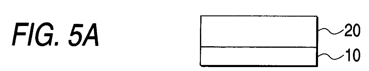
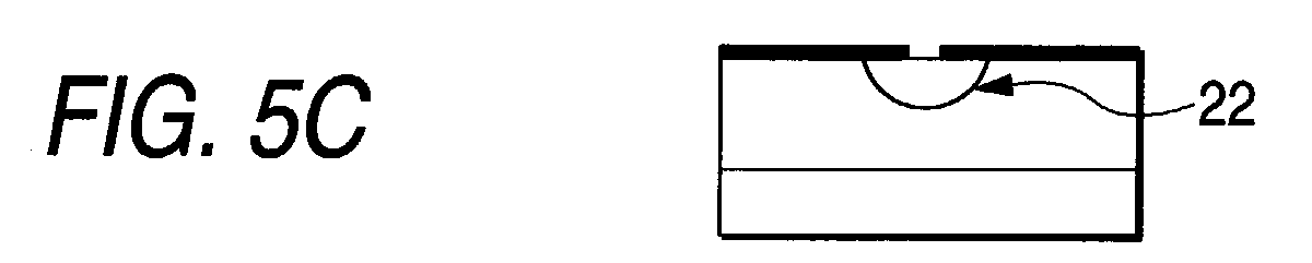
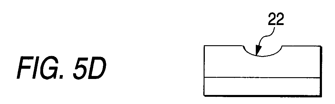
Figs. 5A to 5H show a process for producing a lens array.
While the amount of F added is controlled, an SiO2 layer
20 is formed on a silica glass substrate 10 so that the total
thickness of the SiO2 layer 20 is 200 µm (Fig. 5A). Fig. 6 shows
the etching rate distribution due to etching with an aqueous
solution of 5 % hydrofluoric acid in a direction of the depth
of the layer.
A Cr film 30 is formed on a surface of the SiO2 layer and
a plurality of circular openings 32 each with an opening diameter
of 5 µm are formed like intersections of a grid by photolithography
(Fig. 5B). Incidentally, Fig. 5B shows only one opening for
the sake of simplification. While the Cr layer is used as a
mask, the SiO2 layer is etched with an aqueous solution of
hydrofluoric acid (Fig. 5C). As a result, concave portions 22
each having a sectional shape as shown in Fig. 5D are formed.
Because the lens thickness is defined by the aforementioned
lens design, the whole of the SiO2 layer may be etched again
after the removal of the Cr layer (Fig. 5D) as occasion demands.
The depth of each concave portion is therefore adjusted so that
the lens thickness becomes a defined value (Fig. 5E). If it
is unnecessary to adjust the lens thickness, this step may be
omitted.
Then, the concave portions 24 formed thus are used as a
lens molding tool 50 for producing an aspherical lens array by
molding.
After a releasant is applied to the concave portions 24
of the molding tool 50 produced thus, the concave portions 24
are filled with an ultraviolet-curable resin 40 which will exhibit
a refractive index of 1.41 after curing (Fig. 5F). Then, a 1.0
mm-thick silica glass substrate 12 is pressed against the molding
tool 50 from above (Fig. 5G). In this condition, the resin 40
is irradiated with ultraviolet rays. After the resin 40 is cured,
the resin 40 is released from the molding tool 50 (Fig. 5H).
By the aforementioned steps, a lens array 60 constituted by lenses
each substantially having an aspherical shape can be formed.
The aspherical lenses obtained thus are used for forming
collimators in order to evaluate the characteristic thereof as
follows. A pair of collimators each constituted by a single
mode optical fiber and the produced aspherical lens are disposed
so that the optical axes of the optical fibers coincide with
each other. The pair of collimators are adjusted so that collimated
light rays propagate between the two aspherical lenses. When
insertion loss between the optical fibers is evaluated in this
condition, a sufficiently small value of about 0.2 dB is obtained.
Although the first embodiment has been described on the
case where the amount of F added is controlled continuously,
the amount of F added may be controlled stepwise. Twenty points
are taken at regular intervals in the thicknesswise direction
on the distribution curve in Fig. 6. An amount of F corresponding
to each of the points is added to an SiO2 layer. Twenty fluoridated
SiO2 layers formed in this manner and each having a thickness
of 10 µm are laminated.
When the laminated layer is etched in the same manner as
in the first embodiment, an aspherical lens array can be also
formed. The number of layers to be laminated is not limited
to the aforementioned number.
The film-forming method according to the second embodiment
in which the amount of F added is controlled delicately and stepwise
is slightly complex because a precision flow rate controller
is required. A method simplified so that the number of layers
to be laminated is reduced will be described.
Figs. 8A to 8F show a method for forming one or two homogeneous
layers. After an additive-free SiO2 layer 26 is formed on a silica
glass substrate 10, a predetermined amount of F is added into
an SiO2 layer to form a fluoridated SiO2 layer 28 (Fig. 8A).
Alternatively, the additive-free SiO2 layer 26 may be omitted
so that only one fluoridated SiO2 layer 28 is formed directly
on the silica glass substrate 10. Generally, because an SiO2
layer formed by the CVD method is higher in etching rate with
hydrofluoric acid than a silica glass substrate, an appropriate
etching rate may be sometimes obtained in the case where an
additive-free SiO2 layer is formed on a silica glass substrate
by the CVD method.
A Cr layer 30 is formed on a surface of the fluoridated
SiO2 layer 28 and a plurality of circular openings 32 each having
an opening diameter of 5 µm are formed like intersections of
a grid by photolithography (Fig. 8B). While the Cr layer is
used as a mask, the fluoridated SiO2 layer 28 is etched with
an aqueous solution of hydrofluoric acid (Fig. 8C). Etching
is performed so that the resulting hole pierces the fluoridated
SiO2 layer 28 and reaches the additive-free SiO2 layer 26 located
under the fluoridated SiO2 layer 28 (Fig. 8D). Then, after the
Cr mask is removed, the whole of the surface is etched again
so that the whole of the fluoridated SiO2 layer 28 formed by
the CVD method is removed (Fig. 8E). On this occasion, the depth
of each concave portion 25 is adjusted so that the lens thickness
becomes a defined value.
Though not shown, a lens array is molded in the same manner
as in the first or second embodiment.
When the thickness of the fluoridated SiO2 layer is set
at 200 µm and the etching rate of the fluoridated SiO2 layer
is set at 1.7 times as high as that of the additive-free SiO2
layer, concave portions each having a shape approximately close
to the design value are obtained. Also in the case where the
thickness of the fluoridated SiO2 layer is set at 100 µm and
the etching rate of the fluoridated SiO2 layer is set at 2 times
as high as that of the additive-free SiO2 layer or in the case
where the thickness of the fluoridated SiO2 layer is set at 30
µm and the etching rate of the fluoridated SiO2 layer is set
at 2.5 times as high as that of the additive-free SiO2 layer,
concave portions each having a shape similar to the aforementioned
shape are obtained.
Aspherical lenses obtained by using the concave portions
as a molding tool are used for forming a collimator optical system
in the same manner as in the first embodiment. When insertion
loss of the collimator optical system is evaluated, a value of
about 0.3 dB which can stand comparison with the value obtained
in the first embodiment is obtained.
Although the embodiments have been described on the case
where an SiO2 layer exhibiting an etching rate distribution is
formed by a CVD method, the film-forming method is not limited
thereto. For example, a vacuum vapor deposition method, or a
high-density plasma assist vapor deposition method may be used.
Although the embodiments have been described on the case
where the change of the etching rate of a fluoridated SiO2 film
due to etching with an aqueous solution of hydrofluoric acid
is utilized, the producing method according to the invention
is not limited thereto. Various etching means are provided in
accordance with materials to be etched. Besides the liquid-phase
etching means, reactive ion etching means or chemical or physical
etching means such as laser ablation performed in gas phase may
be used. If materials different in etching rate with respect
to these etching means are used, the same processing as described
above can be made.
Although the embodiments have been described on the case
where concave portions formed by etching are used as a molding
tool for forming resin convex lenses on a substrate, the form
of each lens is not limited thereto. Because all the processed
SiO2 materials are transparent, the concave portions filled with
a high-refractive-index resin may be used directly so as to function
as a convex lens array. Alternatively, each of the processed
concave portions may be used directly as an aspherical concave
lens.
The aspherical structure which can be molded is not limited
to a lens array but may be a single lens. The invention is,
however, remarkably effective in simultaneously producing a
plurality of identical shapes compared with the related art.
This is because variation in dimension in a large number of elements
is caused by abrasion of a cutter if a molding tool constituted
by the large number of elements is producedby related-art machining
but processing can be however carried out with considerable
accuracy if a molding tool constituted by a single element is
produced by related-art machining.
If a reflecting film of a metal or the like is formed on
each of the formed concave portions, an aspherical concave mirror
can be formed as another product than the lens. Further, if
the opening shape of the mask is not circular but stripe-like,
groove-like concave portions can be formed. If the etching rate
distribution is adjusted, the groove-like concave portions can
be used as groove members each having a desired sectional shape.
The groove members can be used for holding cylindrical optical
components such as optical fibers. Further, concave portions
each having a nearly elliptic sectional shape with a depth larger
than a width, which were particularly hardly produced in the
related art, can be formed so that the surface shape of each
concave portion becomes any shape such as a circular shape, or
a groove shape. Such an aspherical structure is used effectively
for micro optical components, micro fluid applied components,
etc. Further, the groove-like concave portions may be used as
a molding tool for forming lenticular lenses each having a modified
circular shape in section.
When a layer exhibiting an etching rate distribution is
etched through a mask, a molding tool for molding an aspherical
structure accurately or an aspherical structure itself can be
formed. The invention is particularly effectively applied to
molding of an aspherical lens array.
In addition, although the layer exhibiting the etching rate
distribution is formed on a substrate, and that layer is etched,
the present invention should not be restricted thereto or thereby.
For example, a layer having an etching rate different from an
etching rate of a substrate may be formed on the substrate, and
not only that layer but also the substrate may be etched. In
this case, that layer and the substrate combined together form
a layer exhibiting an etching rate distribution.
Figs . 9A to 9E are views for explaining a method of producing
an aspherical lens molding tool according to the invention in
processing sequence. First, as shown in Fig. 9A, a homogenous
layer 2 different in etching rate from a silica glass substrate
1 is formed on the surface of the silica glass substrate 1.
Fig. 11 shows the variation of the etching rate ratio of
the CVD film to the silica glass substrate in accordance with
the CF4 flow rate for each concentration of the aqueous solution
of hydrofluoric acid. It is understood that the etching rate
ratio of the CVD film to the silica glass substrate can be varied
also by changing the concentration of the aqueous solution of
hydrofluoric acid (HF) for use in etching.
On the basis of this result, an SiO2 film is formed in the
CVD method with the CF4 flow rate being constant and hence with
the amount of F added being constant, while the concentration
of the aqueous solution of hydrofluoric acid is selected. Hence,
an SiO2 layer having a selected etching rate ratio to the substrate
can be formed.
For example, the layer 2 is formed in the CVD method so
as to satisfy the following relationship. That is, the etching
rate ratio of the layer 2 to the silica glass substrate 1 is
2.5 when the layer 2 having a thickness of 30 µm is etched with
an aqueous solution of 5 wt% hydrofluoric acid. The etching
rate ratio of the layer 2 to the silica glass substrate 1 is
2.0 when the layer 2 having a thickness of 100 µm is etched with
an aqueous solution of 20 wt% hydrofluoric acid. The etching
rate ratio of the layer 2 to the silica glass substrate 1 is
1.7 when the layer 2 having a thickness of 200 µm is etched with
an aqueous solution of 49 wt% hydrofluoric acid.
As shown in Fig. 11, the etching rate ratio is not limited
to that in this embodiment. The etching rate ratio is variable
in a range of 1.1-11.0, and the film thickness can be set in
a range of 1-1,000 µm.
Incidentally, although the layer 2 is formed in the CVD
method in this embodiment, an ion plating method or a vacuum
deposition method may be used.
Next, as shown in Fig. 9A, a Cr film is deposited, and a
mask 3 made of Cr and having a circular opening with a diameter
of 5 µm is then formed in a photolithography method. Although
Cr is used as the material of the mask in this embodiment, a
material using Ti, ITO or A1 as its base may be used.
Next, wet etching is performed using an aqueous solution
of hydrofluoric acid. As shown in Fig. 9B, etching proceeds
isotropically up to the interface between the layer 2 and the
silica glass substrate 1. After that, when the etching has
proceeded to reach the interface between the layer 2 and the
silica glass substrate 1, continuously anisotropic etching
proceeds as shown in Fig. 9C because the etching rate in the
silica glass substrate 1 is slower than that in the layer 2.
When the mask is removed after the wet etching, a groove having
an aspherical portion is obtained as shown in Fig. 9D.
Next, wet etching with the aqueous solution of hydrofluoric
acid is performed on the laminate of the silica glass substrate
1 and the layer 2 again without forming any mask on the surface
of the silica glass substrate 1 in which the groove having an
aspherical portion has been formed. This wet etching is continued
till at least the layer 2 is removed completely. By performing
etching in two stages as described above, a concave portion 1A
having a larger curvature radius than that when the first stage
of etching has been finished can be formed (Fig. 9E) . The concave
portion 1A has a shape so that the depth of the deepest portion
of the concave portion 1A is smaller than 1/2 of the width of
the concave portion 1A. In addition, since the layer 2 having
a constant curvature is removed, the formed concave portion has
an aspherical shape in which the curvature increases continuously
as the location goes farther toward an end portion of the concave
portion, that is, the curvature becomes larger at the point B1
or B2 than that at the point B2 or B3, as shown in Fig. 10.
In addition, as shown in Fig. 12A, a mask 4 (made of Cr)
having a plurality of circular openings is formed, and two stages
of etching are carried out in the aforementioned manner. Thus,
an aspherical lens array molding tool 5 having a plurality of
concave portions 5A is obtained as shown in Fig. 12B.
An aspherical lens array molding tool 5 having a plurality
of concave portions 5A is obtained thus as shown in Fig. 13A.
Ultraviolet-curing type transparent epoxy-based resin 7 is
dripped onto the aspherical lens array molding tool 5 as shown
in Fig. 13B. Then, the aspherical lens array molding tool 5
is covered with a lens substrate 6 so as to be filled with the
epoxy-based resin 7. The epoxy-based resin 7 is irradiated with
ultraviolet rays so as to be cured. Thus, an aspherical lens
array 8 like a flat plate can be formed as shown in Fig. 13C.
When epoxy-based resin having a higher refractive index than
that of the aspheric lens array molding tool 5 and that of the
lens substrate 6 is selected as the epoxy-based resin 7, a lens
effect can be obtained between the epoxy-based resin 7 and the
aspherical lens array molding tool 5. It is desired that
epoxy-based resin whose refractive index is not lower than 1.65
is used as the epoxy-based resin 7.
A releasant 9 is applied to an aspherical lens array molding
tool 5 obtained in the same manner and having a plurality of
concave portions 5A as shown in Fig. 14A. Ultraviolet-curing
type transparent epoxy-based resin 10 is dripped onto the
aspherical lens array molding tool 5 as shown in Fig. 14B. Then,
the aspherical lens array molding tool 5 is covered with a lens
substrate 6 so as to be filled with the epoxy-based resin 10
as shown in Fig. 14C. The epoxy-based resin 10 is irradiated
with ultraviolet rays so as to be cured. The plurality of concave
portions 5A of the aspherical lens array molding tool 5 have
been transferred to the epoxy-based resin 10. Thus, when the
epoxy-based resin 10 is released from the aspherical lens array
molding tool 5, an aspherical lens array 11 constituted by the
epoxy-based resin 10 and the lens substrate 6 can be formed as
shown in Fig. 14D.
It is desired that epoxy-based resin whose refractive index
is higher than that of the air and equal to that of the lens
substrate 6 is used as the epoxy-based resin 10.
Although epoxy-based resin is used in this embodiment,
acrylic-based resin may be used. In addition, the
ultraviolet-curing type resin may be replaced by a thermosetting
type or photo-curing type transparent material.
In addition, although a mask having a circular opening is
used in this embodiment, a mask having a rectangular opening
in place of the circular opening may be used to form a concave
portion which is aspheric in section.
As described above, according to the invention, a homogenous
layer different in etching rate from a substrate is formed on
the surface of the substrate, and wet etching is carried out
on the laminate of the substrate and the layer by use of a mask.
Thus, it is possible to form a molding tool having an aspherical
concave portion and an aspherical lens array.
Claims (30)
- A method of producing an aspherical structure, comprising the steps of:forming a layer on a surface of a planar substrate so that said layer exhibits an etching rate distribution in a direction perpendicular to said surface of said planar substrate with respect to predetermined etching means;forming a mask having a predetermined opening shape on a surface of said layer; andetching said layer through'said mask for a predetermined time by said predetermined etching means to thereby form at least one concave portion.
- A method of producing an aspherical structure, comprising the steps of:forming a layer on a surface of a planar substrate so that said layer exhibits an etching rate distribution in a direction perpendicular to said surface of said planar substrate with respect to predetermined etching means;forming a mask having a predetermined opening shape on a surface of said layer;etching said layer through said mask for a predetermined time by said predetermined etching means to thereby form at least one concave portion; andfilling said concave portion with a fluid substance and solidifying said fluid substance.
- A method of producing an aspherical structure, comprising the steps of:forming a layer on a surface of a planar substrate so that said layer exhibits an etching rate distribution in a direction perpendicular to said surface of said planar substrate with respect to predetermined etching means;forming a mask having a predetermined opening shape on a surface of said layer;etching said layer through said mask for a predetermined time by said predetermined etching means to thereby form at least one concave portion;filling said concave portion with a fluid substance and solidifying said fluid substance; andremoving the solidified substance from said concave portion.
- Amethod of producing an aspherical structure according to any one of Claims 1, 2 and 3, wherein said etching rate distribution is a continuous distribution.
- A method of producing an aspherical structure according to any one of Claims 1, 2 and 3, wherein said etching rate distribution is a stepped distribution.
- An aspherical lens array molding tool produced by a producing method according to Claim 1, wherein:said mask has a plurality of circular openings as said opening shape of said mask; andsaid layer exhibiting an etching rate distribution is etched through said mask.
- An aspherical lens array produced by a producing method according to Claim 2, wherein:said mask has a plurality of circular openings as said opening shape of said mask; andsaid layer exhibiting an etching rate distribution and said fluid substance are provided as transparent members.
- An aspherical lens array produced by a producing method according to Claim 3, wherein:said mask has a plurality of circular openings as said opening shape of said mask; andsaid fluid substance is provided as a transparent member.
- A product that can be used as a molding tool for forming an aspherical convex lens, or as an aspherical concave lens, comprising:a substrate;a layer on said substrate, the layer having a gradient etching rate distribution in which the rate of etching with a specific chemical substance changes from the outermost surface of the layer toward said substrate;at least one concave portion formed in said layer and recessed from the outermost surface toward said substrate, said concave portion having an aspherical surface.
- The product according to claim 9, wherein said etching rate distribution is a continuous distribution.
- The product according to claim 9, wherein said etching rate distribution is a stepped distribution.
- The product according to claim 9, wherein said layer is mainly made of a glass material comprising SiO2 with fluorine as additive.
- The product according to claim 12, wherein the additive amount of the fluorine changes from the outermost layer toward said substrate.
- The product according to claim 9, wherein the layer includes a single layer in which the etching rate changes continuously.
- The product according to claim 9, wherein the layer includes multiple layers, each having a respective constant etching rate, thereby providing a stepped etching rate distribution as a whole of the multiple layers.
- The product according to claim 9, wherein said at least one concave portion includes a plurality of the concave portions having the same shape and dimension.
- A method of producing an aspherical lens molding tool, comprising the steps of:forming a homogeneous layer on a surface of a substrate, said layer being different in etching rate from said substrate;forming a mask on said layer, said mask having an opening shape;etching said layer and said substrate through said mask;removing said mask; andetching said layer and said substrate again to remove at least said layer and form a concave portion.
- A method of producing an aspherical lens molding tool according to Claim 17, wherein a material higher in etching rate than said substrate is selected as a material for forming said layer.
- A method of producing an aspherical lens molding tool according to Claim 17, wherein a ratio of etching rate of said layer to etching rate of said substrate is 1.1-11.0.
- An aspherical lens molding tool produced by a method of producing an aspherical lens molding tool according to any one of Claims 17 to 19.
- An aspherical lens molding tool according to Claim 20, wherein said concave portion has a shape in which depth of a deepest portion of said concave portion is smaller than 1/2 of width of said concave portion.
- An aspherical lens molding tool according to Claim 20, wherein said concave portion has a shape having a curvature radius larger in a portion closer to an end portion of said concave portion.
- A method of producing an aspherical lens, comprising the step of:filling a concave portion of an aspherical lens molding tool according to any one of Claims 20 to 22 with a fluid substance, and solidifying said fluid substance.
- A method of producing an aspherical lens, comprising the steps of:filling a concave portion of an aspherical lens molding tool according to any one of Claims 20 to 22 with a fluid substance, and solidifying said fluid substance; andremoving said solidified substance from said concave portion
- An aspherical lens array molding tool comprising an aspherical lens molding tool according to any one of Claims 20 to 22, said molding tool being provided with a plurality of concave portions similar to said concave portion.
- An aspherical lens array comprising a plurality of aspherical lenses produced by a method of producing an aspherical lens according to Claim 23, wherein said fluid substance to be solidified is a transparent resin having a higher refractive index than that of said molding tool.
- An aspherical lens array comprising a plurality of aspherical lenses produced by a method of producing an aspherical lens according to Claim 24, wherein said fluid substance to be solidified is a transparent resin having a higher refractive index than that of the air.
- A method of producing an aspherical structure, comprising the steps of:providing a first layer having a first etching rate;providing a second layer on the first layer, the second layer having a second etching rate different from the first etching rate;etching the first layer to expose a part of the second layer; andfurther etching the first layer and the second layer to form an aspherical concave portion.
- A method of claim 28, wherein the step of providing the first layer includes forming the first layer on a substrate.
- A method of claim 28, wherein the step of providing the first layer includes providing a substrate as the first layer.
Applications Claiming Priority (4)
| Application Number | Priority Date | Filing Date | Title |
|---|---|---|---|
| JP2002009395 | 2002-01-18 | ||
| JP2002009395A JP2003211462A (en) | 2002-01-18 | 2002-01-18 | Method for manufacturing aspherical surface structure, molding tool for aspherical surface lens array and aspherical surface lens array |
| JP2002087039A JP3885631B2 (en) | 2002-03-26 | 2002-03-26 | Method of manufacturing aspheric lens mold, aspheric lens array mold manufactured by the method, and aspheric lens array |
| JP2002087039 | 2002-03-26 |
Publications (1)
| Publication Number | Publication Date |
|---|---|
| EP1329432A1 true EP1329432A1 (en) | 2003-07-23 |
Family
ID=26625562
Family Applications (1)
| Application Number | Title | Priority Date | Filing Date |
|---|---|---|---|
| EP03000691A Withdrawn EP1329432A1 (en) | 2002-01-18 | 2003-01-17 | Method for producing aspherical structure, and aspherical lens array molding tool and aspherical lens array produced by the same method |
Country Status (4)
| Country | Link |
|---|---|
| US (1) | US7329372B2 (en) |
| EP (1) | EP1329432A1 (en) |
| CA (1) | CA2416746A1 (en) |
| TW (1) | TW200302355A (en) |
Cited By (4)
| Publication number | Priority date | Publication date | Assignee | Title |
|---|---|---|---|---|
| EP1731928A2 (en) * | 2005-06-07 | 2006-12-13 | Yin S. Tang | Motionless lens systems and methods |
| US7572385B2 (en) * | 2003-11-17 | 2009-08-11 | Micron Technology, Inc. | Method of forming micro-lenses |
| GB2492398A (en) * | 2011-06-30 | 2013-01-02 | Fusion Optix Inc | Manufacturing an optical composite using inverted light collimating surface features |
| FR3137187A1 (en) * | 2022-06-28 | 2023-12-29 | Commissariat A L'energie Atomique Et Aux Energies Alternatives | Process for manufacturing concave microcavities |
Families Citing this family (27)
| Publication number | Priority date | Publication date | Assignee | Title |
|---|---|---|---|---|
| US20060131784A1 (en) * | 2003-01-10 | 2006-06-22 | Takaki Sugimoto | Flexible mold, method of manufacturing same and method of manufacturing fine structures |
| JP4380522B2 (en) * | 2004-02-06 | 2009-12-09 | 日本ビクター株式会社 | Manufacturing method of replica mold for microlens array |
| US20050211665A1 (en) * | 2004-03-26 | 2005-09-29 | Sharp Laboratories Of America, Inc. | Methods of forming a microlens array |
| FR2870471B1 (en) * | 2004-05-18 | 2006-08-25 | Briot Internat Sa | METHOD OF GROOVING OR CONTRABESAUTING THE PERIPHERY OF AN OPHTHALMIC LENS |
| JP4417926B2 (en) * | 2006-03-06 | 2010-02-17 | カシオ計算機株式会社 | Method for flattening glass substrate |
| CN101373224A (en) * | 2007-08-24 | 2009-02-25 | 鸿富锦精密工业(深圳)有限公司 | Method for making film coating glasses lens |
| WO2009069467A1 (en) * | 2007-11-29 | 2009-06-04 | Konica Minolta Opto, Inc. | Imaging lens, imaging device, and portable terminal |
| CN101909865A (en) * | 2008-01-08 | 2010-12-08 | Lg伊诺特有限公司 | Lens unit, lens assembly, camera module, method of fabricating camera module and lens assembly, method of fabricating optic member, and apparatus for fabricating optic member |
| KR101634353B1 (en) * | 2008-12-04 | 2016-06-28 | 삼성전자주식회사 | Micro lens, method for manufacturing the micro lens, apparatus for manufacturing the micro lens, camera module including the micro lens |
| CN101885577A (en) * | 2009-05-14 | 2010-11-17 | 鸿富锦精密工业(深圳)有限公司 | Mold, press molding device and method for molding micro concave lens array by impressing |
| KR20100130423A (en) * | 2009-06-03 | 2010-12-13 | 삼성전자주식회사 | Wafer-level lens module and image module including the same |
| KR101648540B1 (en) * | 2009-08-13 | 2016-08-16 | 삼성전자주식회사 | Wafer-level lens module and imaging device including the same |
| US8305699B2 (en) * | 2009-09-23 | 2012-11-06 | Samsung Electronics Co., Ltd. | Wafer-level lens module with extended depth of field and imaging device including the wafer-level lens module |
| AU2012211170B2 (en) | 2011-01-28 | 2015-02-19 | Crane & Co., Inc. | A laser marked device |
| US8557149B2 (en) * | 2011-04-08 | 2013-10-15 | Uchicago Argonne, Llc | System and method for implementing enhanced optics fabrication |
| RU2641316C9 (en) * | 2011-08-19 | 2019-03-21 | Визуал Физикс, Ллс | Optionally transferable optical system with reduced thickness |
| CA2881826C (en) | 2012-08-17 | 2021-03-30 | Visual Physics, Llc | A process for transferring microstructures to a final substrate |
| US10173453B2 (en) | 2013-03-15 | 2019-01-08 | Visual Physics, Llc | Optical security device |
| US9873281B2 (en) | 2013-06-13 | 2018-01-23 | Visual Physics, Llc | Single layer image projection film |
| BR112016021736A2 (en) | 2014-03-27 | 2017-08-15 | Visual Physics Llc | OPTICAL DEVICE PRODUCING SPARKLING-TYPE OPTICAL EFFECTS |
| US10766292B2 (en) | 2014-03-27 | 2020-09-08 | Crane & Co., Inc. | Optical device that provides flicker-like optical effects |
| MX2017000681A (en) | 2014-07-17 | 2018-03-12 | Visual Physics Llc | An improved polymeric sheet material for use in making polymeric security documents such as banknotes. |
| KR102497982B1 (en) | 2014-09-16 | 2023-02-09 | 크레인 시큐리티 테크놀로지스, 인크. | Secure lens layer |
| CN107003431B (en) | 2015-01-27 | 2019-03-12 | 麦克赛尔株式会社 | The manufacturing method of non-rotational symmetry lens/reflecting mirror and its shaping dies |
| RU2712604C2 (en) | 2015-02-11 | 2020-01-29 | КРАНЕ и КО., ИНК. | Method of applying protective device on substrate surface |
| KR102489526B1 (en) | 2017-02-10 | 2023-01-17 | 크레인 앤 코, 인크 | Machine-readable optical security device |
| CN114606468B (en) * | 2022-03-11 | 2023-03-31 | 业成科技(成都)有限公司 | Non-spherical film sputtering system |
Citations (12)
| Publication number | Priority date | Publication date | Assignee | Title |
|---|---|---|---|---|
| EP0146160A1 (en) * | 1983-11-15 | 1985-06-26 | Koninklijke Philips Electronics N.V. | Method of manufacturing a geodesic construction element and optical integrated system comprising such an element |
| JPH01257901A (en) * | 1988-04-08 | 1989-10-16 | Dainippon Printing Co Ltd | Formation of micro-condenser lens of solid-state image pickup element |
| EP0620201A2 (en) * | 1993-04-12 | 1994-10-19 | Hughes Aircraft Company | Method of manufacturing mircro-optical elements |
| JPH07104106A (en) * | 1993-10-04 | 1995-04-21 | Asahi Glass Co Ltd | Production of aspherical microlens array |
| US5549212A (en) * | 1993-12-28 | 1996-08-27 | Nec Corporation | Method for forming rough surface with controlled convex shape |
| JPH08241891A (en) * | 1994-06-13 | 1996-09-17 | Ind Technol Res Inst | Method of improving spin-on-glass layer on substrate |
| JPH1126899A (en) * | 1997-06-30 | 1999-01-29 | Casio Comput Co Ltd | Alloy wiring and its forming method |
| EP0911144A2 (en) * | 1997-10-22 | 1999-04-28 | Micro Optics Company Ltd. | Stamper for use in forming planar micro-lens array and method of forming thereof |
| EP1022108A1 (en) * | 1997-12-26 | 2000-07-26 | Nippon Sheet Glass Co., Ltd. | Erecting life-size resin lens array and method of manufacturing it |
| EP1069082A2 (en) * | 1999-07-15 | 2001-01-17 | Eastman Kodak Company | Method and apparatus for compression moulding glass microlens arrays |
| WO2002006560A1 (en) * | 2000-07-18 | 2002-01-24 | National Institute Of Advanced Industrial Science And Technology | Graded material and method for synthesis thereof and method for processing thereof |
| US20020084251A1 (en) * | 2000-07-25 | 2002-07-04 | Neal Ricks | Method of making a 3-D structure using an erodable mask formed from a film having a composition that varies in its direction of thickness |
Family Cites Families (1)
| Publication number | Priority date | Publication date | Assignee | Title |
|---|---|---|---|---|
| JPH05150103A (en) * | 1991-11-29 | 1993-06-18 | Asahi Glass Co Ltd | Production of aspherical microlens array |
-
2003
- 2003-01-17 TW TW092101174A patent/TW200302355A/en unknown
- 2003-01-17 EP EP03000691A patent/EP1329432A1/en not_active Withdrawn
- 2003-01-17 US US10/346,053 patent/US7329372B2/en not_active Expired - Fee Related
- 2003-01-20 CA CA002416746A patent/CA2416746A1/en not_active Abandoned
Patent Citations (12)
| Publication number | Priority date | Publication date | Assignee | Title |
|---|---|---|---|---|
| EP0146160A1 (en) * | 1983-11-15 | 1985-06-26 | Koninklijke Philips Electronics N.V. | Method of manufacturing a geodesic construction element and optical integrated system comprising such an element |
| JPH01257901A (en) * | 1988-04-08 | 1989-10-16 | Dainippon Printing Co Ltd | Formation of micro-condenser lens of solid-state image pickup element |
| EP0620201A2 (en) * | 1993-04-12 | 1994-10-19 | Hughes Aircraft Company | Method of manufacturing mircro-optical elements |
| JPH07104106A (en) * | 1993-10-04 | 1995-04-21 | Asahi Glass Co Ltd | Production of aspherical microlens array |
| US5549212A (en) * | 1993-12-28 | 1996-08-27 | Nec Corporation | Method for forming rough surface with controlled convex shape |
| JPH08241891A (en) * | 1994-06-13 | 1996-09-17 | Ind Technol Res Inst | Method of improving spin-on-glass layer on substrate |
| JPH1126899A (en) * | 1997-06-30 | 1999-01-29 | Casio Comput Co Ltd | Alloy wiring and its forming method |
| EP0911144A2 (en) * | 1997-10-22 | 1999-04-28 | Micro Optics Company Ltd. | Stamper for use in forming planar micro-lens array and method of forming thereof |
| EP1022108A1 (en) * | 1997-12-26 | 2000-07-26 | Nippon Sheet Glass Co., Ltd. | Erecting life-size resin lens array and method of manufacturing it |
| EP1069082A2 (en) * | 1999-07-15 | 2001-01-17 | Eastman Kodak Company | Method and apparatus for compression moulding glass microlens arrays |
| WO2002006560A1 (en) * | 2000-07-18 | 2002-01-24 | National Institute Of Advanced Industrial Science And Technology | Graded material and method for synthesis thereof and method for processing thereof |
| US20020084251A1 (en) * | 2000-07-25 | 2002-07-04 | Neal Ricks | Method of making a 3-D structure using an erodable mask formed from a film having a composition that varies in its direction of thickness |
Non-Patent Citations (4)
| Title |
|---|
| DATABASE WPI Section EI Week 199647, Derwent World Patents Index; Class U11, AN 1996-474285, XP002234085 * |
| PATENT ABSTRACTS OF JAPAN vol. 014, no. 008 (P - 987) 10 January 1990 (1990-01-10) * |
| PATENT ABSTRACTS OF JAPAN vol. 1995, no. 07 31 August 1995 (1995-08-31) * |
| PATENT ABSTRACTS OF JAPAN vol. 1999, no. 04 30 April 1999 (1999-04-30) * |
Cited By (9)
| Publication number | Priority date | Publication date | Assignee | Title |
|---|---|---|---|---|
| US7572385B2 (en) * | 2003-11-17 | 2009-08-11 | Micron Technology, Inc. | Method of forming micro-lenses |
| US8361332B2 (en) | 2003-11-17 | 2013-01-29 | Micron Technology, Inc. | Method of forming micro-lenses |
| US7535649B2 (en) | 2004-03-09 | 2009-05-19 | Tang Yin S | Motionless lens systems and methods |
| US7706071B2 (en) | 2004-03-09 | 2010-04-27 | Tang Yin S | Lens systems and methods |
| EP1731928A2 (en) * | 2005-06-07 | 2006-12-13 | Yin S. Tang | Motionless lens systems and methods |
| EP1731928A3 (en) * | 2005-06-07 | 2006-12-20 | Yin S. Tang | Motionless lens systems and methods |
| GB2492398A (en) * | 2011-06-30 | 2013-01-02 | Fusion Optix Inc | Manufacturing an optical composite using inverted light collimating surface features |
| FR3137187A1 (en) * | 2022-06-28 | 2023-12-29 | Commissariat A L'energie Atomique Et Aux Energies Alternatives | Process for manufacturing concave microcavities |
| EP4299506A1 (en) * | 2022-06-28 | 2024-01-03 | Commissariat à l'énergie atomique et aux énergies alternatives | Method of making concave microcavity |
Also Published As
| Publication number | Publication date |
|---|---|
| US20030157211A1 (en) | 2003-08-21 |
| CA2416746A1 (en) | 2003-07-18 |
| TW200302355A (en) | 2003-08-01 |
| US7329372B2 (en) | 2008-02-12 |
Similar Documents
| Publication | Publication Date | Title |
|---|---|---|
| US7329372B2 (en) | Method for producing aspherical structure, and aspherical lens array molding tool and aspherical lens array produced by the same method | |
| US7113336B2 (en) | Microlens including wire-grid polarizer and methods of manufacture | |
| JP5024047B2 (en) | Manufacturing method of microstructure | |
| US5114513A (en) | Optical device and manufacturing method thereof | |
| US10823889B2 (en) | Partially etched phase-transforming optical element | |
| KR102421825B1 (en) | Multi-level diffractive optical element thin film coating | |
| US20150029588A1 (en) | Control of Light Wavefronts | |
| KR20140035936A (en) | Image relay waveguide and method of producing same | |
| US20040247010A1 (en) | Antireflection diffraction grating | |
| JP2004012856A (en) | Optical element, mold for optical element, and method for manufacturing optical element | |
| US20080037124A1 (en) | Optical Member And Manufacturing Method Thereof | |
| US20030155327A1 (en) | Manufacturing method for optical integrated circuit having spatial reflection type structure | |
| US20190339423A1 (en) | Optical component and method of manufacturing optical component | |
| CN114488365A (en) | Far infrared superlens and processing method thereof | |
| US6903877B2 (en) | Gradient-index lens, and method for producing the same | |
| JP3885631B2 (en) | Method of manufacturing aspheric lens mold, aspheric lens array mold manufactured by the method, and aspheric lens array | |
| JP2003211462A (en) | Method for manufacturing aspherical surface structure, molding tool for aspherical surface lens array and aspherical surface lens array | |
| JP4457589B2 (en) | Optical apparatus having a transmissive optical element | |
| JP2002355826A (en) | Method for producing lens part for optical communication | |
| JP2003262713A (en) | Diffraction optical element and method for manufacturing diffraction optical element | |
| JP3726790B2 (en) | Manufacturing method of micro lens array | |
| JP4279598B2 (en) | Manufacturing method of gradient index lens | |
| US20200156335A1 (en) | Low birefrigence, molded optical components | |
| CN114371521A (en) | Super-surface optical device covered with reflecting layer, optical equipment and manufacturing method | |
| JP2005161563A (en) | Manufacturing method for aspheric shaped article and aspheric lens array formed by transferring aspheric shaped article |
Legal Events
| Date | Code | Title | Description |
|---|---|---|---|
| PUAI | Public reference made under article 153(3) epc to a published international application that has entered the european phase |
Free format text: ORIGINAL CODE: 0009012 |
|
| AK | Designated contracting states |
Designated state(s): AT BE BG CH CY CZ DE DK EE ES FI FR GB GR HU IE IT LI LU MC NL PT SE SI SK TR |
|
| AX | Request for extension of the european patent |
Extension state: AL LT LV MK RO |
|
| AKX | Designation fees paid | ||
| REG | Reference to a national code |
Ref country code: DE Ref legal event code: 8566 |
|
| STAA | Information on the status of an ep patent application or granted ep patent |
Free format text: STATUS: THE APPLICATION IS DEEMED TO BE WITHDRAWN |
|
| 18D | Application deemed to be withdrawn |
Effective date: 20040124 |