EP1281663A3 - Method of manufacture of micromechanical structures - Google Patents
Method of manufacture of micromechanical structures Download PDFInfo
- Publication number
- EP1281663A3 EP1281663A3 EP02012141A EP02012141A EP1281663A3 EP 1281663 A3 EP1281663 A3 EP 1281663A3 EP 02012141 A EP02012141 A EP 02012141A EP 02012141 A EP02012141 A EP 02012141A EP 1281663 A3 EP1281663 A3 EP 1281663A3
- Authority
- EP
- European Patent Office
- Prior art keywords
- silicon wafer
- structures
- etching process
- layer
- masking layer
- Prior art date
- Legal status (The legal status is an assumption and is not a legal conclusion. Google has not performed a legal analysis and makes no representation as to the accuracy of the status listed.)
- Withdrawn
Links
Classifications
-
- B—PERFORMING OPERATIONS; TRANSPORTING
- B81—MICROSTRUCTURAL TECHNOLOGY
- B81C—PROCESSES OR APPARATUS SPECIALLY ADAPTED FOR THE MANUFACTURE OR TREATMENT OF MICROSTRUCTURAL DEVICES OR SYSTEMS
- B81C1/00—Manufacture or treatment of devices or systems in or on a substrate
- B81C1/00388—Etch mask forming
- B81C1/00428—Etch mask forming processes not provided for in groups B81C1/00396 - B81C1/0042
-
- B—PERFORMING OPERATIONS; TRANSPORTING
- B81—MICROSTRUCTURAL TECHNOLOGY
- B81C—PROCESSES OR APPARATUS SPECIALLY ADAPTED FOR THE MANUFACTURE OR TREATMENT OF MICROSTRUCTURAL DEVICES OR SYSTEMS
- B81C1/00—Manufacture or treatment of devices or systems in or on a substrate
- B81C1/00777—Preserve existing structures from alteration, e.g. temporary protection during manufacturing
- B81C1/00785—Avoid chemical alteration, e.g. contamination, oxidation or unwanted etching
- B81C1/00801—Avoid alteration of functional structures by etching, e.g. using a passivation layer or an etch stop layer
-
- B—PERFORMING OPERATIONS; TRANSPORTING
- B81—MICROSTRUCTURAL TECHNOLOGY
- B81C—PROCESSES OR APPARATUS SPECIALLY ADAPTED FOR THE MANUFACTURE OR TREATMENT OF MICROSTRUCTURAL DEVICES OR SYSTEMS
- B81C1/00—Manufacture or treatment of devices or systems in or on a substrate
- B81C1/00865—Multistep processes for the separation of wafers into individual elements
- B81C1/00896—Temporary protection during separation into individual elements
Abstract
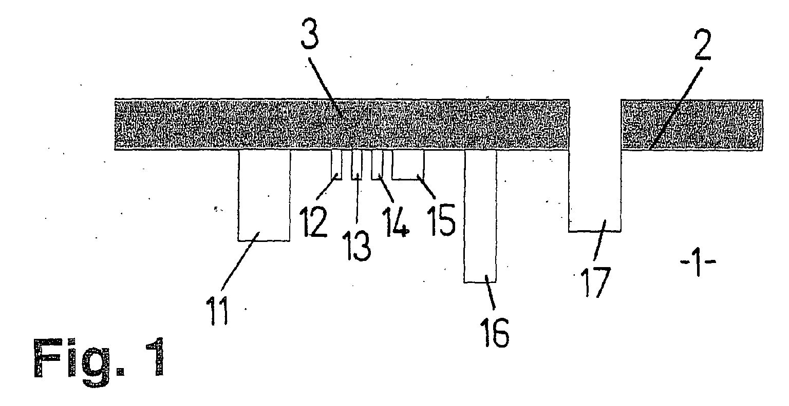
Mit der vorliegenden Erfindung wird ein Verfahren vorgeschlagen, mit dem unterschiedliche Strukturen, wie z.B. Grobstrukturen und Feinstrukturen, unabhängig voneinander in einem Siliziumwafer oder in der Funktionsschicht eines Schichtaufbaus für Oberflächenmikromechanik erzeugt werden können.With the present invention, a method is proposed, with the different Structures such as e.g. Coarse structures and fine structures, independent from each other in a silicon wafer or in the functional layer of a layer structure can be generated for surface micromechanics.
Dazu wird der Siliziumwafer (1) bzw. die Funktionsschicht zunächst mit mindestens
einer ersten Maskierschicht versehen, die so strukturiert wird, dass ein
Teil der zu erzeugenden Strukturen (11 bis 17) in einem Ätzvorgang erzeugt werden
kann. Der so maskierte Siliziumwafer (1) bzw. die so maskierte Funktionsschicht
wird dann mindestens einem ersten Ätzvorgang unterzogen, nach dem die
entsprechende erste Maskierschicht entfernt wird. Erfindungsgemäß wird der Siliziumwafer
(1) bzw. die Funktionsschicht nach dem mindestens einen ersten Ätzvorgang
und dem Entfernen der mindestens einen ersten Maskierschicht mindestens
einmal mit einer weiteren Maskierschicht (3) versehen, so dass die bereits
erzeugten Strukturen (11 bis 16) gegen einen weiteren Ätzangriff geschützt sind.
Diese weitere Maskierschicht (3) wird strukturiert, bevor der so maskierte Siliziumwafer
(1) bzw. die so maskierte Funktionsschicht einem weiteren Ätzvorgang
unterzogen wird und die weitere Maskierschicht (3) nach dem weiteren Ätzvorgang
entfernt wird.
Applications Claiming Priority (2)
| Application Number | Priority Date | Filing Date | Title |
|---|---|---|---|
| DE10136016 | 2001-07-24 | ||
| DE2001136016 DE10136016A1 (en) | 2001-07-24 | 2001-07-24 | Process for generating micromechanical structures |
Publications (2)
| Publication Number | Publication Date |
|---|---|
| EP1281663A2 EP1281663A2 (en) | 2003-02-05 |
| EP1281663A3 true EP1281663A3 (en) | 2005-03-02 |
Family
ID=7692904
Family Applications (1)
| Application Number | Title | Priority Date | Filing Date |
|---|---|---|---|
| EP02012141A Withdrawn EP1281663A3 (en) | 2001-07-24 | 2002-06-01 | Method of manufacture of micromechanical structures |
Country Status (2)
| Country | Link |
|---|---|
| EP (1) | EP1281663A3 (en) |
| DE (1) | DE10136016A1 (en) |
Families Citing this family (1)
| Publication number | Priority date | Publication date | Assignee | Title |
|---|---|---|---|---|
| DE102006060205B3 (en) * | 2006-12-18 | 2008-04-17 | Forschungszentrum Jülich GmbH | Substrate's e.g. wafer, plated-through hole and strip conductor producing method, involves producing plated-through hole and strip conductor simultaneously on one side of substrate by further deposition of metal |
Citations (7)
| Publication number | Priority date | Publication date | Assignee | Title |
|---|---|---|---|---|
| EP0418423A1 (en) * | 1989-09-22 | 1991-03-27 | Siemens Aktiengesellschaft | Process for etching silicon anisotropically |
| EP0718878A2 (en) * | 1994-12-24 | 1996-06-26 | Alcatel SEL Aktiengesellschaft | Manufacturing process of conductors on a substrate with depressions |
| US5919713A (en) * | 1994-01-28 | 1999-07-06 | Fujitsu Limited | Semiconductor device and method of making |
| JP2000127100A (en) * | 1998-09-10 | 2000-05-09 | Trw Inc | Micro working method for wafer |
| JP2000164890A (en) * | 1998-11-27 | 2000-06-16 | Denso Corp | Semiconductor kinematic value sensor and manufacturing method therefor |
| EP1049143A2 (en) * | 1999-04-29 | 2000-11-02 | Lg Electronics Inc. | Etching method |
| US6225145B1 (en) * | 1998-09-07 | 2001-05-01 | Electronics And Telecommunications Research Institute | Method of fabricating vacuum micro-structure |
Family Cites Families (3)
| Publication number | Priority date | Publication date | Assignee | Title |
|---|---|---|---|---|
| US5859655A (en) * | 1995-10-30 | 1999-01-12 | International Business Machines Corporation | Photoresist for use in ink jet printers and other micro-machining applications |
| US5738757A (en) * | 1995-11-22 | 1998-04-14 | Northrop Grumman Corporation | Planar masking for multi-depth silicon etching |
| DE19606537A1 (en) * | 1996-02-22 | 1997-08-28 | Bosch Gmbh Robert | Process for producing a master structure |
-
2001
- 2001-07-24 DE DE2001136016 patent/DE10136016A1/en not_active Ceased
-
2002
- 2002-06-01 EP EP02012141A patent/EP1281663A3/en not_active Withdrawn
Patent Citations (7)
| Publication number | Priority date | Publication date | Assignee | Title |
|---|---|---|---|---|
| EP0418423A1 (en) * | 1989-09-22 | 1991-03-27 | Siemens Aktiengesellschaft | Process for etching silicon anisotropically |
| US5919713A (en) * | 1994-01-28 | 1999-07-06 | Fujitsu Limited | Semiconductor device and method of making |
| EP0718878A2 (en) * | 1994-12-24 | 1996-06-26 | Alcatel SEL Aktiengesellschaft | Manufacturing process of conductors on a substrate with depressions |
| US6225145B1 (en) * | 1998-09-07 | 2001-05-01 | Electronics And Telecommunications Research Institute | Method of fabricating vacuum micro-structure |
| JP2000127100A (en) * | 1998-09-10 | 2000-05-09 | Trw Inc | Micro working method for wafer |
| JP2000164890A (en) * | 1998-11-27 | 2000-06-16 | Denso Corp | Semiconductor kinematic value sensor and manufacturing method therefor |
| EP1049143A2 (en) * | 1999-04-29 | 2000-11-02 | Lg Electronics Inc. | Etching method |
Non-Patent Citations (4)
| Title |
|---|
| BRUGGER J ET AL: "Microfabricated ultrasensitive piezoresistive cantilevers for torque magnetometry", SENSORS AND ACTUATORS A, ELSEVIER SEQUOIA S.A., LAUSANNE, CH, vol. 73, no. 3, 30 March 1999 (1999-03-30), pages 235 - 242, XP004167986, ISSN: 0924-4247 * |
| PATENT ABSTRACTS OF JAPAN vol. 2000, no. 08 6 October 2000 (2000-10-06) * |
| PATENT ABSTRACTS OF JAPAN vol. 2000, no. 09 13 October 2000 (2000-10-13) * |
| SURIADI A ET AL: "Photolithography on micromachined 3D surfaces using spray coating technology of photoresist", PROCEEDINGS OF THE SPIE, LITHOGRAPHY FOR SEMICONDUCTOR MANUFACTURING II, 30 MAY - 1 JUNE 2001, EDINBURGH, UK, vol. 4404, 30 May 2001 (2001-05-30) - 1 June 2001 (2001-06-01), USA, pages 245 - 253, XP002312493, ISSN: 0277-786X * |
Also Published As
| Publication number | Publication date |
|---|---|
| EP1281663A2 (en) | 2003-02-05 |
| DE10136016A1 (en) | 2003-04-03 |
Similar Documents
| Publication | Publication Date | Title |
|---|---|---|
| DE60021909T2 (en) | STAMPING FORM LITHOGRAPH | |
| DE19680590B4 (en) | Method for producing acceleration sensors | |
| DE102007026372B4 (en) | Method for forming a microstructure in a semiconductor device | |
| EP1696477A3 (en) | Process of fabrication of sub-lithographic structures | |
| DE102008060644A1 (en) | Production of a Graphanenanovorrichtung | |
| DE10223729B4 (en) | A method of manufacturing a semiconductor device capable of detecting a dynamic quantity | |
| DE4232821C2 (en) | Process for producing a finely structured semiconductor component | |
| EP1532071B1 (en) | Layer system comprising a silicon layer and a passivation layer, method for producing a passivation layer on a silicon layer and the use of said system and method | |
| DE10224137A1 (en) | Etching gas and dry etching method | |
| DE102008037947B4 (en) | Method for producing an element wafer and an element | |
| DE102005030449A1 (en) | Floating gate electrode formation method of flash memory device, involves patterning organic bottom anti-reflection coating film using photoresist patterns | |
| EP1281663A3 (en) | Method of manufacture of micromechanical structures | |
| EP0783107B1 (en) | Manufacturing process for a micromechanical element with movable structure | |
| DE19819456B4 (en) | Method for producing a micromechanical component | |
| DE112010004602T5 (en) | A treatment solution for preventing a pattern collapse in a fine metal structure body and a method for producing a fine metal structure body using the same | |
| EP0599074B1 (en) | Method for the global planarization of surfaces of integrated semiconductor circuits | |
| WO2003102690B1 (en) | Method for producing photoresist masks for structuring semiconductor substrates by means of optical lithography | |
| WO2002009176A2 (en) | Method for applying adjusting marks on a semiconductor disk | |
| EP1071981B1 (en) | Method for producing large-surface membrane masks | |
| DE102013223490A1 (en) | Process for producing a structured surface | |
| DE10349764B4 (en) | Hard mask for structuring a layer and method for generating a hard mask for structuring a layer | |
| DE102017206828A1 (en) | Mechanical damper for a stack of substrates; Method for producing a mechanical damper | |
| DE10002363B4 (en) | Process for producing a micromechanical structure | |
| DE10202513B4 (en) | Self-cleaning surfaces for imaging sensors | |
| DE10312202B4 (en) | Method for producing an etching mask on a microstructure, in particular a semiconductor structure with trench capacitors, and corresponding use of the etching mask |
Legal Events
| Date | Code | Title | Description |
|---|---|---|---|
| PUAI | Public reference made under article 153(3) epc to a published international application that has entered the european phase |
Free format text: ORIGINAL CODE: 0009012 |
|
| AK | Designated contracting states |
Designated state(s): AT BE CH CY DE DK ES FI FR GB GR IE IT LI LU MC NL PT SE TR |
|
| AX | Request for extension of the european patent |
Extension state: AL LT LV MK RO SI |
|
| PUAL | Search report despatched |
Free format text: ORIGINAL CODE: 0009013 |
|
| AK | Designated contracting states |
Kind code of ref document: A3 Designated state(s): AT BE CH CY DE DK ES FI FR GB GR IE IT LI LU MC NL PT SE TR |
|
| AX | Request for extension of the european patent |
Extension state: AL LT LV MK RO SI |
|
| AKX | Designation fees paid | ||
| REG | Reference to a national code |
Ref country code: DE Ref legal event code: 8566 |
|
| STAA | Information on the status of an ep patent application or granted ep patent |
Free format text: STATUS: THE APPLICATION IS DEEMED TO BE WITHDRAWN |
|
| 18D | Application deemed to be withdrawn |
Effective date: 20050903 |