EP1262017B1 - Spectral distortion monitor for controlling pre-distortion and feed-forward linearization of rf power amplifier - Google Patents
Spectral distortion monitor for controlling pre-distortion and feed-forward linearization of rf power amplifier Download PDFInfo
- Publication number
- EP1262017B1 EP1262017B1 EP01912738A EP01912738A EP1262017B1 EP 1262017 B1 EP1262017 B1 EP 1262017B1 EP 01912738 A EP01912738 A EP 01912738A EP 01912738 A EP01912738 A EP 01912738A EP 1262017 B1 EP1262017 B1 EP 1262017B1
- Authority
- EP
- European Patent Office
- Prior art keywords
- signal
- port
- output
- amplifier
- coupled
- Prior art date
- Legal status (The legal status is an assumption and is not a legal conclusion. Google has not performed a legal analysis and makes no representation as to the accuracy of the status listed.)
- Expired - Lifetime
Links
Images
Classifications
-
- H—ELECTRICITY
- H03—ELECTRONIC CIRCUITRY
- H03F—AMPLIFIERS
- H03F3/00—Amplifiers with only discharge tubes or only semiconductor devices as amplifying elements
- H03F3/20—Power amplifiers, e.g. Class B amplifiers, Class C amplifiers
-
- H—ELECTRICITY
- H03—ELECTRONIC CIRCUITRY
- H03F—AMPLIFIERS
- H03F1/00—Details of amplifiers with only discharge tubes, only semiconductor devices or only unspecified devices as amplifying elements
- H03F1/32—Modifications of amplifiers to reduce non-linear distortion
- H03F1/3223—Modifications of amplifiers to reduce non-linear distortion using feed-forward
- H03F1/3229—Modifications of amplifiers to reduce non-linear distortion using feed-forward using a loop for error extraction and another loop for error subtraction
-
- H—ELECTRICITY
- H03—ELECTRONIC CIRCUITRY
- H03F—AMPLIFIERS
- H03F1/00—Details of amplifiers with only discharge tubes, only semiconductor devices or only unspecified devices as amplifying elements
- H03F1/32—Modifications of amplifiers to reduce non-linear distortion
- H03F1/3241—Modifications of amplifiers to reduce non-linear distortion using predistortion circuits
- H03F1/3247—Modifications of amplifiers to reduce non-linear distortion using predistortion circuits using feedback acting on predistortion circuits
Definitions
- the present invention relates in general to radio frequency (RF) communication systems, and is particularly directed to an RF power amplifier linearization mechanism, that employs a spectral distortion measurement and differential combining scheme, which is operative to optimize the operation of a carrier cancellation combiner, and pre-distortion and feed-forward loops of the RF power amplifier, so that intermodulation distortion produced at the output of the RF amplifier may be minimized.
- RF radio frequency
- Attenuating sidebands sufficiently to meet industry or regulatory-based standards using such modulation techniques requires very linear signal processing systems and components. Although relatively linear components can be obtained at a reasonable cost for relatively low bandwidth (baseband) telephone networks, linearizing components such as RF power amplifiers can be prohibitively expensive.
- IMDs intermodulation distortion products
- a fundamental difficulty in linearizing an RF power amplifier is the fact that it is an inherently non-linear device, and generates unwanted intermodulation distortion products (IMDs).
- IMDs manifest themselves as spurious signals in_the amplified RF output signal, separate and distinct from the RF input signal.
- a further manifestation of IMD is spectral regrowth or spreading of a compact spectrum into spectral regions that were not occupied by the RF input signal. This distortion causes the phase-amplitude of the amplified output signal to depart from the phase-amplitude of the input signal, and may be considered as an incidental (and undesired) amplifier-sourced modulation of the RF input signal.
- a straightforward way to implement a linear RF power amplifier is to build it as a large, high power device, but operate the amplifier at only a low power level (namely, at a small percentage of its rated output power), where the RF amplifier's transfer function is relatively linear.
- An obvious drawback to this approach is the overkill penalty -a costly and large sized RF device.
- Other prior art techniques which overcome this penalty include feedback correction techniques, feedforward correction, and pre-distortion correction. Feedforward and predistortion correction, however, are not limited in this regard.
- Feedback correction techniques include polar envelope correction (such as described in U.S. Patent No. 5,742,201 ), and Cartesian feedback, where the distortion component at the output of the RF amplifier is used to directly modulate the input signal to the amplifier in real time.
- Feedback techniques possess the advantage of self-convergence, as do negative feedback techniques in other fields of design.
- systems which employ negative feedback remain stable over a limited bandwidth, which prevents their application in wide-bandwidth environments, such as multi-carrier or W-CDMA.
- error present in the RF amplifier's output signal is extracted, amplified to the proper level, and then reinjected with equal amplitude but opposite phase into the output path of the amplifier, so that (ideally) the RF amplifier's distortion is effectively canceled.
- predistortion correction a signal is modulated onto the RF input signal path upstream of the RF amplifier.
- the ideal predistortion signal has a characteristic that is the inverse or complement of the distortion expected at the output of the high power RF amplifier, so that when subjected to the distorting transfer function of the RF amplifier, it effectively cancels the distortion behavior.
- Either predistortion or feedforward may be made adaptive by extracting an error signal component in the output of the RF amplifier and then adjusting the control signal(s), in accordance with the extracted error behavior of the RF amplifier, so as to effectively continuously minimize distortion in the amplifier's output.
- pilot tone a pilot (tone) signal into the signal flow path through the amplifier and measure the amplifier's response.
- a fundamental drawback to the use of a pilot tone is the need for dedicated pilot generation circuitry and the difficulty of placing the pilot tone within the signal bandwidth of the amplifier.
- pilot tone injection causes the generation of an unwanted spur; also, a piloted system is open-loop in the sense that the controller operates on the pilot and not the IMDs. Hence, the system only assumes that IMDs are being properly cancelled.
- the present invention consists in an RF power amplifier arrangement comprising:
- the present invention consists in a method of measuring and compensating for distortion in an RF power amplifier coupled in an RF signal processing path between an RF input port to which an RF input signal is coupled and an RF output port from which an amplified RF output signal is derived, said method being characterized by the steps of:
- the operation of a carrier cancellation combiner, and pre-distortion and feed-forward loops of an RF power amplifier are controlled to minimize IMD components at the output of the RF amplifier, by a spectral distortion measurement scheme that performs (Fast Fourier Transform (FFT) - based) spectral power measurements at a 'reference' signal port (associated with the RF input signal), and a plurality of 'test' signal ports (associated with various parameter adjustment locations of the amplifier).
- FFT Fast Fourier Transform
- Averaged FFT's of the data extracted from the reference port and data from the test ports by a digital signal processor based controller provide spectral information for each sampled signal set.
- the control data FFT is processed to establish a baseline, with which the test data FFTs are compared to generate adjustment signals for various control parameters, through which IMDs introduced by the amplifier are minimized.
- the performance of the RF amplifier is continuously monitored and the control parameters modified as necessary to compensate for drift in the amplifier's characteristics.
- the invention includes digitally controlled gain and phase adjustment circuits and a digitally controlled predistortion unit incorporated in the RF input signal path to a main RF amplifier.
- the predistortion unit may contain a work function-based vector modulator that is coupled to receive weighting coefficients from the controller. Since it contains any intermodulation (spectral regrowth) distortion products (IMDs) introduced by the RF amplifier, the output of the amplifier is monitored as one of the test inputs to the controller.
- IMDs intermodulation (spectral regrowth) distortion products
- the output of the main RF amplifier is further coupled to a carrier cancellation combiner, a second input of which is coupled to a feed forward path from the RF input signal port.
- the feed forward path from the RF input signal port includes a fixed delay and a variable delay unit, that serve to substantially equalize the propagation delay of the signal path through the main RF amplifier, and thereby provide proper phase alignment of the signals applied to the carrier cancellation combiner.
- the output of the carrier cancellation combiner is coupled to gain and phase adjustment circuits of a feed forward error amplifier, the output of which is reinjected into the output path of the RF amplifier, for feed-forward IMD cancellation.
- the DSP-based controller performs various spectral distortion measurement operations, and error minimization algorithms such as, but not limited to power or least mean squared minimization, to control variable gain and phase shift components in both the main RF amplifier and error amplifier signal paths, for the purpose of optimally canceling IMD components at the RF output port. It also generates work function-based predistortion control signals derived from respectively different work functions of the instantaneous amplitude of the RF input signal, so as to predistort phase and amplitude components of the RF input signal to the main RF amplifier.
- the DSP controller is operative to process the spectral data samples derived from the control and test ports, and then adjusts the parameters of the control components as necessary to compensate for main RF amplifier distortion.
- the controller FFT-processes the control data to identify any carriers present in the RF input signal, and the noise floor. FFT-processing the data allows spectral energy in one or more frequency bins, other than the portion of the spectrum in which the carrier components are located, to be selectively discarded, to avoid erroneously influencing the carrier cancellation loop.
- Maximizing this expression has the effect of reducing the average energy in the identified residual carrier components at the output of carrier cancellation combiner to as close to zero as possible (optimal carrier cancellation), without subjecting the maximization operation to the influence of frequency spurs in bins other those containing the carrier(s).
- the FFT of the control data is subtracted from the FFT of the of RF output signal monitored downstream of the feed forward reinjection port.
- the new and improved RF power amplifier spectral measurement and distortion correction mechanism resides primarily in a prescribed arrangement of conventional RF circuits, associated digital signal processing components and attendant supervisory control circuitry, that controls the operation of such circuits and components.
- the configuration of such circuit components, and the manner in which they interface with other communication system equipment have, for the most part, been illustrated in the drawings by a readily understandable block diagram, which shows only those details that are pertinent to the present invention, so as not to obscure the disclosure with details which will be readily apparent to those skilled in the art having the benefit of the description herein.
- the block diagram illustration is primarily intended to show the components in a convenient functional grouping, whereby the invention may be more readily understood.
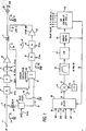
- an RF power amplifier spectral measurement and distortion correction scheme in accordance with the present invention is diagrammatically illustrated as comprising an RF input port 11, to which an RF signal RF in to be amplified is coupled.
- RF input port 11 is coupled over an input signal path 13 to a main RF power amplifier (or basic power module (BPM) 20, whose non-linear spectral distortion (IMD) introducing behavior is to be compensated.
- the input signal path 13 to RF amplifier 20 includes digitally controlled gain and phase adjustment circuits 14 and 15, respectively, and a digitally controlled predistortion unit 16.
- the digitally controlled predistortion unit 16 may contain a work function-based vector modulator, that is coupled to receive a set of weighting coefficients w 0 , w 1 , w 2 , ..., w N , supplied by a performance monitoring and parameter-updating digital signal processor (DSP)-based controller 50.
- DSP digital signal processor
- the DSP controller 50 executes spectral distortion measurement and error minimization algorithms (to be described) for adjusting the pre-distortion properties of predistortion unit 16, and also controls the digitally controlled gain and phase adjustment circuits 14 and 15 of the input signal path, digitally controlled gain and phase adjustment circuits 44 and 45 of a feed forward loop 43 to an error amplifier 40, and an adjustable delay unit 22 that is coupled in a feed forward path 23 to a carrier cancellation combiner 60, as will be described.
- the control lines 51 from controller 50 are denoted by subscripts associated with the respective components being controlled.
- the output of the RF power amplifier 20 is coupled through a downstream delay unit 17 and circulator 18 to an RF output port RF out .
- An RF output directional coupler 19 is coupled to the output path of the amplifier by means of a feed forward reinjection directional coupler 47.
- RF output directional coupler 19 serves as a test signal port that is employed to extract a signal 'OUT', representative of the composite amplified RF signal, including intermodulation (spectral regrowth) distortion products (IMDs) introduced by the RF amplifier, and reductions therein due to the feed forward injection.
- IMDs intermodulation (spectral regrowth) distortion products
- This extracted RF output signal (OUT) is coupled from the directional coupler 19 to a first input 31 of a DSP-controlled switch 30.
- the RF input port 11 is coupled through a directional coupler 21 to a second input 32 of controlled switch 30.
- the output 35 of the switch 30 is coupled to a first input 71 of a mixer 70, a second input 72 of which is coupled to receive an IF frequency provided by a local oscillator 75.
- the mixer 70 is operative to down-convert the output of the switch 30 to baseband.
- This baseband signal is then filtered in a bandpass filter 76, digitized by a high speed analog-to-digital converter (ADC) 77, and then stored in a buffer memory 79 for analysis by the DSP controller 50, as will be described.
- ADC analog-to-digital converter
- the steering operation of switch 30 and read/write control of memory 79 are controlled by a control link 52 from the DSP 50 controller.
- the feed forward path 23 to the carrier cancellation combiner 60 (which may be configured as a Wilkinson combiner) includes a fixed delay line 24 coupled in series with the variable delay unit 22 from the RF input path 13 to a first input 61 of the carrier cancellation combiner 60.
- the second input port 62 of the carrier cancellation combiner 60 is coupled via a directional coupler 25 to the output of the RF amplifier 20.
- the delay is employed to substantially equalize the propagation delay of the feed forward path with the RF signal path through the RF amplifier to a second input port 62 of the RF carrier cancellation combiner 60 and ensure phase alignment of the signals applied to the combiner.
- the carrier cancellation combiner 60 cancels RF carrier components at its output, so as to produce a signal 'Eamp' representative of the IMD portion of the output of the RF amplifier 20.
- the signal Eamp is coupled to respective digitally controlled gain and phase adjustment circuits 44 and 45 to the error amplifier 40, whose output is reinjected into the output path of RF amplifier 20 by the directional coupler 47 installed upstream of directional coupler 19, as described above.
- the signal Eamp is extracted via a further test port directional coupler 65, installed with the feed forward loop 43 at the output of the carrier cancellation combiner 60, and coupled to a third input 33 of the controlled switch 30.
- An additional directional test port coupler 46 is coupled to the path from the directional coupler 25 at the output of the main RF amplifier 20, so as to provide a further signal 'BPM' representative of the amplified output of amplifier 20 to fourth input 34 of controlled switch 30.
- the DSP-based controller 50 uses various spectral distortion measurement operations, and error minimization algorithms (e.g., power or least mean squared minimization) for controlling variable gain and phase shift components in both the main RF amplifier and error amplifier signal paths, for the purpose of optimally canceling IMD components at the RF output port RF out . It also generates work function-based predistortion control signals derived from respectively different work functions of the instantaneous amplitude of the RF input signal to predistort phase and amplitude components of the RF input signal to the main RF amplifier.
- error minimization algorithms e.g., power or least mean squared minimization
- the DSP controller 50 executes what are effectively (Fast Fourier Transform (FFT)-based) spectral power measurements in portions or bins of the frequency spectrum of each of the monitored reference port signal 'SRC', and test port signals 'OUT', 'Eamp', and 'BPM', downconverted to baseband, bandpass filtered, sampled and then stored as a picture or 'snapshot' of the spectral composition of the entire band.
- FFT Fast Fourier Transform
- Averaged FFT's of reference data samples (associated with the SRC port) and respective sets of test data samples (associated with the OUT, Eamp and BPM ports) are performed to obtain the spectral information for each sampled signal set of a respective spectral snapshot.
- the control (SRC) data is processed to establish a baseline, with which the test data is compared to produce adjustment signals for the various control parameters, and thereby minimize IMDs introduced by the main RF amplifier. With the control parameters initially corrected, the performance of the main RF amplifier is thereafter continuously monitored and the adjustable parameters as necessary to compensate for any drift in the amplifier's characteristics.
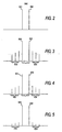
- the DSP controller FFT-processes the SRC data to identify any carriers present in the RF input signal, such as those shown at 201 and 202 in the spectral diagram Figure 2 , and the noise floor.
- FFT DSP controller
- FFT processing of the carrier cancellation test data (Eamp) will typically produce a spectral distribution as shown in the spectral diagram of Figure 3 , which includes (reduced amplitude) residual carrier components 301 and 302 (respectively associated with the carriers 201 and 202 of Figure 2 ), as well as spurious (IMD) components shown in spectral regions or bins 303 and 304 outside the spectral region containing the carriers, the energy content of which should not contribute to carrier cancellation.
- IMD spurious
- maximizing the expression (1) has the effect of reducing the average energy in the identified residual carrier components at the output of carrier cancellation combiner 60 to as close to zero as possible (optimal carrier cancellation), without influencing the maximization operation to energy in spurious components in frequency bins other those containing the carriers.
- this provides a direct measure of carrier cancellation (with both IMDs and carriers being measured simultaneously), the system effectively 'knows' whether or not it is functioning properly - which is not achievable with conventional correlator-based or power-detector energy minimization approaches.
- the present invention obviates the need for additional circuitry to 'interrupt' the control loop under this condition, and eliminates zero-input drift.
- the use of the adjustable delay element 22 allows the invention to detect and optimally tune the delay for any signal misalignment, thereby maximizing carrier cancellation.
- Pre-Distortion Test Data: BPM
- the DSP controller 50 FFT-processes the SRC data to identify any carriers present in the RF input signal, as shown in the spectral diagram Figure 2 , and the noise floor.
- FFT processing of the pre-distortion test data (BPM) will typically produce a spectral distribution as shown in the spectral diagram of Figure 4 , having amplified carrier components 401 and 402 (respectively associated with the carriers 201 and 202 of Figure 2 ) , as well as IMD components shown in regions 403 and 404, that lie outside the spectral region of the carriers.
- EAMP may be employed as the test port in place of the BPM port, since each contains the same IMD information.
- the present invention enables IMD's to be minimized in the presence of carrier, it avoids the problems of carrier energy removal-based approaches, which require some amount of carrier energy removal in order to detect changes in the pre-distortion circuitry, and therefore suffer performance monitoring degradation as more carrier energy is leaked.
- the DSP controller 50 FFT-processes the SRC data to identify any carriers present in the RF input signal ( Figure 2 ) and the noise floor.
- FFT processing of the feed-forward data (OUT) will typically produce a spectral distribution as shown in the spectral diagram of Figure 5 , including amplified carrier components 501 and 502 (respectively associated with the carriers 201 and 202 of Figure 2 ), as well as (reduced amplitude) IMD components shown in regions 503 and 504, that lie outside the spectral region of the carriers.
- the spectral reduction mechanism of the-invention is particularly advantageous with respect to pilot tone based systems that measure amplitude and phase differences of output-delay line and feed-forward path.
- the invention inherently accounts for changes in the amplifier that cause 'targets' of the control loop to drift (and mandate periodic re-calibration of pilot tone systems), and is therefore effectively self-calibrating.
- the invention is wide bandwidth, whereas pilot tone approaches operate only a portion of the band, or operate out-of-band and simply assume that proper cancellation will be performed in the actual band of interest.
- pilot tone based receiver and pilot tone based energy reduction schemes are unable to directly measure IMD performance or detect spurs, and therefore may leave a spur that is 'out-of-spec' to prevent the amplifier's true performance from being seen.
- the present invention is able to minimize IMD's to within a given specification and can directly measure IMD performance.
- the FFT subtraction operations may be replaced by applying the test data to the signal carrier used by the control port.
- the summation operation of each of equations (2) and (3) would then ignore signals already identified at the control port.
Landscapes
- Engineering & Computer Science (AREA)
- Power Engineering (AREA)
- Physics & Mathematics (AREA)
- Nonlinear Science (AREA)
- Amplifiers (AREA)
Abstract
Description
- The present invention relates in general to radio frequency (RF) communication systems, and is particularly directed to an RF power amplifier linearization mechanism, that employs a spectral distortion measurement and differential combining scheme, which is operative to optimize the operation of a carrier cancellation combiner, and pre-distortion and feed-forward loops of the RF power amplifier, so that intermodulation distortion produced at the output of the RF amplifier may be minimized.
- The specifications and regulations of the Federal Communications Commission (FCC) mandate that communication service providers comply with very strict bandwidth constraints, including the requirement that the amount of energy spillover outside a licensed channel or band of interest, be sharply attenuated (e.g., on the order of 50 dB) . Although such limitations may be readily overcome for traditional forms of modulation, such as FM, they are difficult to achieve using more contemporary, digitally based modulation formats, such as M-ary modulation.
- Attenuating sidebands sufficiently to meet industry or regulatory-based standards using such modulation techniques requires very linear signal processing systems and components. Although relatively linear components can be obtained at a reasonable cost for relatively low bandwidth (baseband) telephone networks, linearizing components such as RF power amplifiers can be prohibitively expensive.
- A fundamental difficulty in linearizing an RF power amplifier is the fact that it is an inherently non-linear device, and generates unwanted intermodulation distortion products (IMDs). IMDs manifest themselves as spurious signals in_the amplified RF output signal, separate and distinct from the RF input signal. A further manifestation of IMD is spectral regrowth or spreading of a compact spectrum into spectral regions that were not occupied by the RF input signal. This distortion causes the phase-amplitude of the amplified output signal to depart from the phase-amplitude of the input signal, and may be considered as an incidental (and undesired) amplifier-sourced modulation of the RF input signal.
- A straightforward way to implement a linear RF power amplifier is to build it as a large, high power device, but operate the amplifier at only a low power level (namely, at a small percentage of its rated output power), where the RF amplifier's transfer function is relatively linear. An obvious drawback to this approach is the overkill penalty -a costly and large sized RF device. Other prior art techniques which overcome this penalty include feedback correction techniques, feedforward correction, and pre-distortion correction. Feedforward and predistortion correction, however, are not limited in this regard.
- Feedback correction techniques include polar envelope correction (such as described in
U.S. Patent No. 5,742,201 ), and Cartesian feedback, where the distortion component at the output of the RF amplifier is used to directly modulate the input signal to the amplifier in real time. Feedback techniques possess the advantage of self-convergence, as do negative feedback techniques in other fields of design. However, systems which employ negative feedback remain stable over a limited bandwidth, which prevents their application in wide-bandwidth environments, such as multi-carrier or W-CDMA. - In the feedforward approach, error (distortion) present in the RF amplifier's output signal is extracted, amplified to the proper level, and then reinjected with equal amplitude but opposite phase into the output path of the amplifier, so that (ideally) the RF amplifier's distortion is effectively canceled.
- With predistortion correction, a signal is modulated onto the RF input signal path upstream of the RF amplifier. The ideal predistortion signal has a characteristic that is the inverse or complement of the distortion expected at the output of the high power RF amplifier, so that when subjected to the distorting transfer function of the RF amplifier, it effectively cancels the distortion behavior.
- Either predistortion or feedforward may be made adaptive by extracting an error signal component in the output of the RF amplifier and then adjusting the control signal(s), in accordance with the extracted error behavior of the RF amplifier, so as to effectively continuously minimize distortion in the amplifier's output.
- One conventional mechanism for extracting the error signal component is to inject a pilot (tone) signal into the signal flow path through the amplifier and measure the amplifier's response. A fundamental drawback to the use of a pilot tone is the need for dedicated pilot generation circuitry and the difficulty of placing the pilot tone within the signal bandwidth of the amplifier. In addition, pilot tone injection causes the generation of an unwanted spur; also, a piloted system is open-loop in the sense that the controller operates on the pilot and not the IMDs. Hence, the system only assumes that IMDs are being properly cancelled.
- Other approaches include the use of a high intercept receiver to detect low level distortion in the presence of high power carriers, which adds substantial complexity and cost, or the use of a wideband correlator. The latter mechanism suffers from the fact that it relies on measurement of wideband energy, rather than on the spectral distortion components.
US 5 877 653 teaches a combined predistortion/feedforward RF amplifier with a tunable RSSI detector for adjusting the predistortion feed forward parameters. - According to one aspect, the present invention consists in an RF power amplifier arrangement comprising:
- an RF input port to which an RF input signal is applied;
- an RF output port from which an amplified RF output signal is derived;
- an RF signal processing path coupled between said RF input and output ports, and including an RF power amplifier and an RF distortion correction unit that is controllably operative to adjust one or more parameters of said RF signal processing path so as to compensate for distortion introduced by said RF power amplifier;
- a carrier cancellation combiner having inputs coupled to said RF input port and to an output of said RF amplifier and having an output coupled over a feed forward path through an error amplifier of a reinjection path to said RF output port;
- a reference signal port coupled to said RF input port;
- a first test signal port coupled to said RF output port;
- a second test signal port coupled to said output of said RF amplifier;
- a third test signal port coupled to said output of said carrier cancellation combiner; and
- a Fast Fourier Transform (FFT) signal processor is coupled to derive a set of data representative of the signal composition of the entire band of the signal infrastructure of said amplifier as provided by all of said signals monitored at said reference signal port and said first, second and third test signal ports, and to process said set of data to derive control signals that control modification of said RF input signal by said RF signal processing path and modification of said output of said carrier cancellation combiner by said feed forward path through said error amplifier, in a manner that minimizes distortion introduced by said RF amplifier into said amplified RF output signal.
- According to another aspect, the present invention consists in a method of measuring and compensating for distortion in an RF power amplifier coupled in an RF signal processing path between an RF input port to which an RF input signal is coupled and an RF output port from which an amplified RF output signal is derived, said method being characterized by the steps of:
- (a) providing a Fast Fourier Transform (FFT) distortion correction unit that is controllably operative to adjust one or more parameters of said RF signal processing path to compensate for distortion introduced by said RF power amplifier;
- (b) coupling said RF input port and an output of said RF amplifier to a carrier cancellation combiner having an output coupled over a feed forward path through an error amplifier of a reinjection path to said RF output port;
- (c) coupling a reference signal port coupled to said RF input port;
- (d) coupling a first test signal port coupled to said RF output port;
- (e) coupling a second test signal port coupled to said output of said RF amplifier;
- (f) coupling a third test signal port coupled to said output of said carrier cancellation combiner;
- (g) monitoring signals at said reference signal port and said first, second and third test signal ports;
- (h) deriving a set of data representative of the signal composition of the entire band of the signal infrastructure of said amplifier as provided by all of said signals monitored in step (g) and processing said data to produce control signals (51D22, 51G14, 51P15, 51G16, 51P16, 51G44, 51P45) for controlling modification of said RF input signal by said RF signal processing path and modification of said output of said carrier cancellation combiner by said feed forward path through said error amplifier, that minimizes distortion introduced by said RF amplifier into said amplified RF output signal; and
- (i) controlling modification of said RF input signal by said RF signal processing path and modification of said output of said carrier cancellation combiner by said feed forward path through said error amplifier in accordance with said control signals produced in step (h) so as to minimize distortion introduced by said RF amplifier into said amplified RF output signal.
- In accordance with the present invention, the operation of a carrier cancellation combiner, and pre-distortion and feed-forward loops of an RF power amplifier are controlled to minimize IMD components at the output of the RF amplifier, by a spectral distortion measurement scheme that performs (Fast Fourier Transform (FFT) - based) spectral power measurements at a 'reference' signal port (associated with the RF input signal), and a plurality of 'test' signal ports (associated with various parameter adjustment locations of the amplifier). Signals extracted from the control and test ports are downconverted to baseband, bandpass filtered, sampled and then stored as a spectral 'snapshot' of the entire band of the signal infrastructure of the amplifier.
- Averaged FFT's of the data extracted from the reference port and data from the test ports by a digital signal processor based controller provide spectral information for each sampled signal set. The control data FFT is processed to establish a baseline, with which the test data FFTs are compared to generate adjustment signals for various control parameters, through which IMDs introduced by the amplifier are minimized. The performance of the RF amplifier is continuously monitored and the control parameters modified as necessary to compensate for drift in the amplifier's characteristics.
- In accordance with a preferred, but non-limiting embodiment, the invention includes digitally controlled gain and phase adjustment circuits and a digitally controlled predistortion unit incorporated in the RF input signal path to a main RF amplifier. The predistortion unit may contain a work function-based vector modulator that is coupled to receive weighting coefficients from the controller. Since it contains any intermodulation (spectral regrowth) distortion products (IMDs) introduced by the RF amplifier, the output of the amplifier is monitored as one of the test inputs to the controller.
- The output of the main RF amplifier is further coupled to a carrier cancellation combiner, a second input of which is coupled to a feed forward path from the RF input signal port. The feed forward path from the RF input signal port includes a fixed delay and a variable delay unit, that serve to substantially equalize the propagation delay of the signal path through the main RF amplifier, and thereby provide proper phase alignment of the signals applied to the carrier cancellation combiner. The output of the carrier cancellation combiner is coupled to gain and phase adjustment circuits of a feed forward error amplifier, the output of which is reinjected into the output path of the RF amplifier, for feed-forward IMD cancellation.
- The DSP-based controller performs various spectral distortion measurement operations, and error minimization algorithms such as, but not limited to power or least mean squared minimization, to control variable gain and phase shift components in both the main RF amplifier and error amplifier signal paths, for the purpose of optimally canceling IMD components at the RF output port. It also generates work function-based predistortion control signals derived from respectively different work functions of the instantaneous amplitude of the RF input signal, so as to predistort phase and amplitude components of the RF input signal to the main RF amplifier.
- The DSP controller is operative to process the spectral data samples derived from the control and test ports, and then adjusts the parameters of the control components as necessary to compensate for main RF amplifier distortion. In order to maximize carrier cancellation, the controller (FFT)-processes the control data to identify any carriers present in the RF input signal, and the noise floor. FFT-processing the data allows spectral energy in one or more frequency bins, other than the portion of the spectrum in which the carrier components are located, to be selectively discarded, to avoid erroneously influencing the carrier cancellation loop.
- Optimal (maximum) cancellation of carrier components is accomplished by adjusting the gain and phase adjustment circuits in the RF input signal path and the adjustable delay unit, so as to maximize the expression:

where N is the total number of carriers, Ci is the average power of carrier Ci of N, and Ri is the average power of residual carrier Ri of N. - Maximizing this expression has the effect of reducing the average energy in the identified residual carrier components at the output of carrier cancellation combiner to as close to zero as possible (optimal carrier cancellation), without subjecting the maximization operation to the influence of frequency spurs in bins other those containing the carrier(s).
- To optimally control the pre-distortion components at the input to the main RF amplifier, the FFT of the control data is subtracted from the FFT of the monitored output of the main RF amplifier to obtain the IMD components; then the gain and phase adjustment circuits of the predistortion unit are adjusted to minimize the following expression:

where Di is the distortion component i of N detected spectral components resulting from the subtraction operation. - For optimal feed-forward compensation the FFT of the control data is subtracted from the FFT of the of RF output signal monitored downstream of the feed forward reinjection port. The gain and phase adjustment circuits for the feed forward error amplifier are then adjusted to minimize the following expression:

where Di is the distortion component i of N detected spectral components resulting from the subtraction operation. -
-
Figure 1 diagrammatically illustrates an RF power amplifier spectral measurement and distortion correction scheme in accordance with an embodiment of the invention; and -
Figures 2-5 are respective spectral diagrams associated with the operation of the RF power amplifier arrangement ofFigure 1 . - Before describing in detail the new and improved RF power amplifier spectral measurement and distortion correction mechanism in accordance with the present invention, it should be observed that the invention resides primarily in a prescribed arrangement of conventional RF circuits, associated digital signal processing components and attendant supervisory control circuitry, that controls the operation of such circuits and components. As a result, the configuration of such circuit components, and the manner in which they interface with other communication system equipment have, for the most part, been illustrated in the drawings by a readily understandable block diagram, which shows only those details that are pertinent to the present invention, so as not to obscure the disclosure with details which will be readily apparent to those skilled in the art having the benefit of the description herein. Thus, the block diagram illustration is primarily intended to show the components in a convenient functional grouping, whereby the invention may be more readily understood.
- Referring now to
Figure 1 , a non-limiting embodiment of an RF power amplifier spectral measurement and distortion correction scheme in accordance with the present invention is diagrammatically illustrated as comprising anRF input port 11, to which an RF signal RFin to be amplified is coupled.RF input port 11 is coupled over aninput signal path 13 to a main RF power amplifier (or basic power module (BPM) 20, whose non-linear spectral distortion (IMD) introducing behavior is to be compensated. Theinput signal path 13 toRF amplifier 20 includes digitally controlled gain andphase adjustment circuits 14 and 15, respectively, and a digitally controlled predistortion unit 16. - As a preferred, but not limiting example, the digitally controlled predistortion unit 16 may contain a work function-based vector modulator, that is coupled to receive a set of weighting coefficients w0, w1, w2, ..., wN, supplied by a performance monitoring and parameter-updating digital signal processor (DSP)-based
controller 50. TheDSP controller 50 executes spectral distortion measurement and error minimization algorithms (to be described) for adjusting the pre-distortion properties of predistortion unit 16, and also controls the digitally controlled gain andphase adjustment circuits 14 and 15 of the input signal path, digitally controlled gain andphase adjustment circuits forward loop 43 to anerror amplifier 40, and anadjustable delay unit 22 that is coupled in a feedforward path 23 to acarrier cancellation combiner 60, as will be described. (The control lines 51 fromcontroller 50 are denoted by subscripts associated with the respective components being controlled.) - The output of the
RF power amplifier 20 is coupled through a downstream delay unit 17 andcirculator 18 to an RF output port RFout. An RF outputdirectional coupler 19 is coupled to the output path of the amplifier by means of a feed forward reinjectiondirectional coupler 47. RF outputdirectional coupler 19 serves as a test signal port that is employed to extract a signal 'OUT', representative of the composite amplified RF signal, including intermodulation (spectral regrowth) distortion products (IMDs) introduced by the RF amplifier, and reductions therein due to the feed forward injection. - This extracted RF output signal (OUT) is coupled from the
directional coupler 19 to afirst input 31 of a DSP-controlledswitch 30. In order to enable the DSP controlled 50 to monitor the RF input signal RFin as a reference or control signal 'SRC', theRF input port 11 is coupled through adirectional coupler 21 to asecond input 32 of controlledswitch 30. - The
output 35 of theswitch 30 is coupled to afirst input 71 of amixer 70, asecond input 72 of which is coupled to receive an IF frequency provided by a local oscillator 75. Themixer 70 is operative to down-convert the output of theswitch 30 to baseband. This baseband signal is then filtered in abandpass filter 76, digitized by a high speed analog-to-digital converter (ADC) 77, and then stored in abuffer memory 79 for analysis by theDSP controller 50, as will be described. The steering operation ofswitch 30 and read/write control ofmemory 79 are controlled by acontrol link 52 from theDSP 50 controller. - The feed
forward path 23 to the carrier cancellation combiner 60 (which may be configured as a Wilkinson combiner) includes a fixeddelay line 24 coupled in series with thevariable delay unit 22 from theRF input path 13 to afirst input 61 of thecarrier cancellation combiner 60. Thesecond input port 62 of thecarrier cancellation combiner 60 is coupled via adirectional coupler 25 to the output of theRF amplifier 20. The delay is employed to substantially equalize the propagation delay of the feed forward path with the RF signal path through the RF amplifier to asecond input port 62 of the RFcarrier cancellation combiner 60 and ensure phase alignment of the signals applied to the combiner. - By subtracting the split RF output signal extracted by the
directional coupler 25 at the output of theRF amplifier 20 from the split RF reference or input signal RFin of the feed-forward path 23, thecarrier cancellation combiner 60 cancels RF carrier components at its output, so as to produce a signal 'Eamp' representative of the IMD portion of the output of theRF amplifier 20. The signal Eamp is coupled to respective digitally controlled gain andphase adjustment circuits error amplifier 40, whose output is reinjected into the output path ofRF amplifier 20 by thedirectional coupler 47 installed upstream ofdirectional coupler 19, as described above. - The signal Eamp is extracted via a further test port
directional coupler 65, installed with the feed forwardloop 43 at the output of thecarrier cancellation combiner 60, and coupled to athird input 33 of the controlledswitch 30. An additional directionaltest port coupler 46 is coupled to the path from thedirectional coupler 25 at the output of themain RF amplifier 20, so as to provide a further signal 'BPM' representative of the amplified output ofamplifier 20 tofourth input 34 of controlledswitch 30. - As described briefly above, the DSP-based
controller 50 uses various spectral distortion measurement operations, and error minimization algorithms (e.g., power or least mean squared minimization) for controlling variable gain and phase shift components in both the main RF amplifier and error amplifier signal paths, for the purpose of optimally canceling IMD components at the RF output port RFout. It also generates work function-based predistortion control signals derived from respectively different work functions of the instantaneous amplitude of the RF input signal to predistort phase and amplitude components of the RF input signal to the main RF amplifier. - Pursuant to the present invention, and as will be described below with reference to
Figures 2-5 , theDSP controller 50 executes what are effectively (Fast Fourier Transform (FFT)-based) spectral power measurements in portions or bins of the frequency spectrum of each of the monitored reference port signal 'SRC', and test port signals 'OUT', 'Eamp', and 'BPM', downconverted to baseband, bandpass filtered, sampled and then stored as a picture or 'snapshot' of the spectral composition of the entire band. Averaged FFT's of reference data samples (associated with the SRC port) and respective sets of test data samples (associated with the OUT, Eamp and BPM ports) are performed to obtain the spectral information for each sampled signal set of a respective spectral snapshot. The control (SRC) data is processed to establish a baseline, with which the test data is compared to produce adjustment signals for the various control parameters, and thereby minimize IMDs introduced by the main RF amplifier. With the control parameters initially corrected, the performance of the main RF amplifier is thereafter continuously monitored and the adjustable parameters as necessary to compensate for any drift in the amplifier's characteristics. - In order to maximize carrier cancellation by the RF
carrier cancellation combiner 60, the DSP controller (FFT)-processes the SRC data to identify any carriers present in the RF input signal, such as those shown at 201 and 202 in the spectral diagramFigure 2 , and the noise floor. By limiting the data to only that portion of the spectrum in which carrier components have been identified, other spectral energy outside the carrier frequency region of interest may be discarded, so as to not (erroneously) influence the carrier cancellation operation. - FFT processing of the carrier cancellation test data (Eamp) will typically produce a spectral distribution as shown in the spectral diagram of
Figure 3 , which includes (reduced amplitude)residual carrier components 301 and 302 (respectively associated with thecarriers Figure 2 ), as well as spurious (IMD) components shown in spectral regions orbins phase adjustment circuits 14 and 15 andadjustable delay unit 22, so as to maximize the expression (1):
where N is the total number of carriers,
Ci is the average power of carrier Ci of N, and
Ri is the average power of residual carrier Ri of N.
As can be seen from a comparison of the spectral diagrams ofFigures 2 and 3 , maximizing the expression (1) has the effect of reducing the average energy in the identified residual carrier components at the output ofcarrier cancellation combiner 60 to as close to zero as possible (optimal carrier cancellation), without influencing the maximization operation to energy in spurious components in frequency bins other those containing the carriers. As this provides a direct measure of carrier cancellation (with both IMDs and carriers being measured simultaneously), the system effectively 'knows' whether or not it is functioning properly - which is not achievable with conventional correlator-based or power-detector energy minimization approaches. - Moreover, such conventional power detector energy minimization and correlator based schemes are subject to input drive power and cannot resolve whether power is present or not. The present invention obviates the need for additional circuitry to 'interrupt' the control loop under this condition, and eliminates zero-input drift. In addition, the use of the
adjustable delay element 22 allows the invention to detect and optimally tune the delay for any signal misalignment, thereby maximizing carrier cancellation. - As an alternate method, carrier cancellation may be carried out in accordance with the minimization routine:

where N is the total number of carriers, and Ri equals the residual carrier bins identified in the reference port. All other bins are discarded. Pre-Distortion (Test Data: BPM) - As in the case of carrier cancellation, described above, the DSP controller 50 (FFT)-processes the SRC data to identify any carriers present in the RF input signal, as shown in the spectral diagram
Figure 2 , and the noise floor. FFT processing of the pre-distortion test data (BPM) will typically produce a spectral distribution as shown in the spectral diagram ofFigure 4 , having amplified carrier components 401 and 402 (respectively associated with thecarriers Figure 2 ) , as well as IMD components shown inregions - Optimal pre-distortion is accomplished by first subtracting the FFTSRC of the control data (SRC) from the FFTBPM of the test data (BPM), to obtain the IMD components (in
regions Figure 4 ), and then adjusting the gain andphase adjustment circuits 14 and 15 and predistortion unit 16, so as to minimize the following expression (2) :
where Di is the distortion component i of N detected spectral components resulting from FFTBPM - FFTSRC. - As an alternate pre-distortion method, EAMP may be employed as the test port in place of the BPM port, since each contains the same IMD information.
- Because the present invention enables IMD's to be minimized in the presence of carrier, it avoids the problems of carrier energy removal-based approaches, which require some amount of carrier energy removal in order to detect changes in the pre-distortion circuitry, and therefore suffer performance monitoring degradation as more carrier energy is leaked.
- As in the carrier cancellation and predistortion operations described above, the DSP controller 50 (FFT)-processes the SRC data to identify any carriers present in the RF input signal (
Figure 2 ) and the noise floor. FFT processing of the feed-forward data (OUT) will typically produce a spectral distribution as shown in the spectral diagram ofFigure 5 , including amplifiedcarrier components 501 and 502 (respectively associated with thecarriers Figure 2 ), as well as (reduced amplitude) IMD components shown inregions - Optimal feed-forward compensation is accomplished by first subtracting the FFTSRC of the control data (SRC) from the FFTOUT of the test data (OUT), to obtain the IMD components (in
regions Figure 5 ), and then adjusting the gain andphase adjustment circuits 
where Di is the distortion component i of N detected spectral components resulting from FFTOUT - FFTSRC. - The spectral reduction mechanism of the-invention is particularly advantageous with respect to pilot tone based systems that measure amplitude and phase differences of output-delay line and feed-forward path. The invention inherently accounts for changes in the amplifier that cause 'targets' of the control loop to drift (and mandate periodic re-calibration of pilot tone systems), and is therefore effectively self-calibrating. In addition, the invention is wide bandwidth, whereas pilot tone approaches operate only a portion of the band, or operate out-of-band and simply assume that proper cancellation will be performed in the actual band of interest.
- Also, pilot tone based receiver and pilot tone based energy reduction schemes are unable to directly measure IMD performance or detect spurs, and therefore may leave a spur that is 'out-of-spec' to prevent the amplifier's true performance from being seen. The present invention, on the other hand, is able to minimize IMD's to within a given specification and can directly measure IMD performance.
- In a modification of the architecture of
Figure 1 , for both pre-distortion and feed-forward correction, the FFT subtraction operations may be replaced by applying the test data to the signal carrier used by the control port. The summation operation of each of equations (2) and (3) would then ignore signals already identified at the control port. - While I have shown and described several embodiments in accordance with the present invention, it is to be understood that the same is not limited thereto but is susceptible to numerous changes and modifications as known to a person skilled in the art. I therefore do not wish to be limited to the details shown and described herein, but intend to cover all such changes and modifications as are obvious to one of ordinary skill in the art, the scope of the invention being defined by the claims only.
Claims (14)
- An RF power amplifier arrangement comprising:an RF input port (11) to which an RF input signal (RFin) is applied;an RF output port (18) from which an amplified RF output signal is derived;an RF signal processing path coupled between said RF input (11) and output (18) ports, and including an RF power amplifier (20) and an RF distortion correction unit (50) that is controllably operative to adjust one or more parameters (51) of said RF signal processing path so as to compensate for distortion introduced by said RF power amplifier (20);a carrier cancellation combiner (60) having inputs coupled to said RF input port (11) and to an output of said RF amplifier (20) and having an output (63) coupled over a feed forward path through an error amplifier (40) of a reinjection path (47) to said RF output port (18);a reference signal port (21) coupled to said RF input port (11);a first test signal port (19) coupled to said RF output port (18);a second test signal port (46) coupled to said output of said RF amplifier (20);a third test signal port (65) coupled to said output (63) of said carrier cancellation combiner (60); andcharacterized in that:a Fast Fourier Transform (FFT) signal processor (50) is coupled to derive a set of data representative of the signal composition of the entire band of the signal infrastructure of said amplifier as provided by all of said signals monitored (31,32,33,34) at said reference signal port (21) and said first (19), second (46) and third (65) test signal ports, and to process said set of data to derive control signals (51) that control modification of said RF input signal (RFin) by said RF signal processing path and modification of said output (63) of said carrier cancellation combiner (60) by said feed forward path (43) through said error amplifier(40), in a manner that minimizes distortion introduced by said RF amplifier (20) into said amplified RF output signal (RFout).
- An RF power amplifier arrangement according to claim 1, wherein said signal FFT processor (50) is operative to analyze frequency content of said set of data to derive control signals (51) that control modification of said RF input signal (RFin) by said RF signal processing path and modification of said output (63) of said carrier cancellation combiner (60) by said feed forward path (43) through said error amplifier (40), in accordance with prescribed relationships among selected portions of the analyzed frequency content of said set of data.
- An RF power amplifier arrangement according to claim 2, wherein said FFT signal processor (50) is operative to control (51G16, 51P16) modification of said RF input signal (RFin) by said predistortion unit (16) of said RF signal processing path in accordance with differences between selected spectral components of the frequency content of that portion of said set of data associated with said reference signal port (21) and said second test signal port (46).
- An RF power amplifier arrangement according to claim 2, wherein said FFT signal processor (50) is operative to control modification at said RF input signal (RFin) by said RF signal processing path, in accordance with differences between selected spectral components of said set of data associated with the frequency content of said reference signal port (21) and said third test signal port (65).
- An RF power amplifier arrangement according to claim 4, further including an adjustable delay (22) coupled between said RF input port (11) and an input (61) to said carrier cancellation combiner (60), and wherein said FFT signal processor (50) is operative to adjust said delay (22) in accordance with said differences between selected spectral components of said set of data associated with the frequency content of said reference signal port (21) and said third test signal port (65), so as to maximize carrier cancellation by said carrier cancellation combiner (60).
- An RF power amplifier arrangement according to claim 2, wherein said FFT signal processor (50) is operative to control modification of said RF input signal (RFin) by said feed forward path (43) through said error amplifier (40), in accordance with differences between selected spectral components of said set of data associated with the frequency content of said reference signal port (21) and said first test signal port (19).
- An RF power amplifier arrangement according to claim 1, wherein said FFT signal processor (50) is operative to derive said set of data in accordance with averaged Fourier transforms at each of said signals (31,32,33,34) monitored at said reference signal port (21) and said first (19), second (46) and third (65) test signal ports, and to control modification of said RF input signal (RFin) by said RF signal processing path and modification of said output (63) of said carrier cancellation combiner (60) by said feed forward path (43) through said error amplifier(40), in accordance with prescribed relationships among said averaged Fourier transforms.
- A method of measuring and compensating for distortion in an RF power amplifier (20) coupled in an RF signal processing path between an RF input port (11) to which an RF input signal (RFin) is coupled and an RF output port (18) from which an amplified RF output signal (RFout) is derived, said method being characterized by the steps of:(a) providing a Fast Fourier Transform (FFT) distortion correction unit (50) that is controllably operative to adjust one or more parameters (51) of said RF signal processing path to compensate for distortion introduced by said RF power amplifier (20);(b) coupling said RF input port (11) and an output of said RF amplifier (20) to a carrier cancellation combiner (60) having an output (63) coupled over a feed forward path (43) through an error amplifier (40) of a reinjection path (47) to said RF output port (18);(c) coupling a reference signal port (21) coupled to said RF input port (11);(d) coupling a first test signal port (19) coupled to said RF output port (18);(e) coupling a second test signal port (46) coupled to said output of said RF amplifier (20);(f) coupling a third test signal port (65) coupled to said output (63) of said carrier cancellation combiner (60);(g) monitoring signals (31,32,33,34) at said reference signal port (21) and said first (19), second (46) and third (65) test signal ports;(h) deriving a set of data representative of the signal composition (77) of the entire band of the signal infrastructure of said amplifier as provided by all of said signals monitored in step (g) and processing said data (79,50) to produce control signals (51D22, 51G14, 51 P15, 51G16, 51P16, 51G44, 51P45) for controlling modification of said RF input signal (RFin) by said RF signal processing path and modification of said output (63) of said carrier cancellation combiner (60) by said feed forward path (43) through said error amplifier (40), that minimizes distortion introduced by said RF amplifier (20) into said amplified RF output signal (RFout); and(i) controlling modification of said RF input signal (RFin) by said RF signal processing path and modification of said output (63) of said carrier cancellation combiner (60) by said feed forward path (43) through said error amplifier (40) in accordance with said control signals produced in step (h) so as to minimize distortion introduced by said RF amplifier (20) into said amplified RF output signal (RFout).
- A method according to claim 8, wherein step (h) comprises analyzing frequency content of said set of data, and generating said control signals (51) in accordance with prescribed relationships among selected portions of the analyzed frequency content of said set of data associated with each of said signals (31,32,33,34) monitored at said reference signal port (21) and at said first (19), second (46) and third test (65) signal ports,
- A method according to claim 9, wherein step (h) comprises generating control signals (51) for modifying said RF input signal (RFin) by said predistortion unit (16) of said RF signal processing path in accordance with differences between selected spectral components of that portion of said set of data associated with the frequency content of said reference signal port (21) and said second test signal port (46).
- A method according to claim 9, wherein step (h) comprises generating control signals (51) for modifying said RF input signal (RFin) by said RF signal processing path, in accordance with differences between selected spectral components of the frequency content of that portion of said set of data associated with said reference signal port (21) and said third test signal port (65).
- A method according to claim 11, wherein step (h) further comprises generating control signals (51) for adjusting said delay (22) in accordance with said differences between selected spectral components of that portion of said set of data associated with the frequency content of said reference signal port (21) and said third test signal port (65), so as to maximize carrier cancellation by said carrier cancellation combiner (60).
- A method according to claim 9, wherein step (h) comprises generating controls (51) for modifying said RF input signal (RFin) by said feed forward path (43) through said error amplifier (40), in accordance with differences between selected spectral components of that portion of said set of data associated with the frequency content of said reference signal port (21) and said first test signal port (19).
- A method according to claim 8, wherein step (h) further comprises deriving said set of data in accordance with averaged Fourier transforms of each of said signals (31,32,33,34) monitored at said reference signal port (21) and said first (19), second (46) and third (65) test signal ports, and generating control signals (51) for controlling modification of said RF input signal (RFin) by said RF signal processing path and modification of said output of said carrier cancellation combiner (60) by said feed forward path (43) through said error amplifier (40), in accordance with prescribed relationships among said averaged Fourier transforms.
Applications Claiming Priority (3)
| Application Number | Priority Date | Filing Date | Title |
|---|---|---|---|
| US511877 | 1995-08-04 | ||
| US09/511,877 US6275106B1 (en) | 2000-02-25 | 2000-02-25 | Spectral distortion monitor for controlling pre-distortion and feed-forward linearization of rf power amplifier |
| PCT/US2001/004737 WO2001063748A1 (en) | 2000-02-25 | 2001-02-14 | Spectral distortion monitor for controlling pre-distortion and feed-forward linearization of rf power amplifier |
Publications (3)
| Publication Number | Publication Date |
|---|---|
| EP1262017A1 EP1262017A1 (en) | 2002-12-04 |
| EP1262017A4 EP1262017A4 (en) | 2005-12-28 |
| EP1262017B1 true EP1262017B1 (en) | 2009-08-12 |
Family
ID=24036819
Family Applications (1)
| Application Number | Title | Priority Date | Filing Date |
|---|---|---|---|
| EP01912738A Expired - Lifetime EP1262017B1 (en) | 2000-02-25 | 2001-02-14 | Spectral distortion monitor for controlling pre-distortion and feed-forward linearization of rf power amplifier |
Country Status (8)
| Country | Link |
|---|---|
| US (1) | US6275106B1 (en) |
| EP (1) | EP1262017B1 (en) |
| JP (1) | JP4913304B2 (en) |
| KR (1) | KR20030010583A (en) |
| AT (1) | ATE439700T1 (en) |
| AU (1) | AU2001241485A1 (en) |
| DE (1) | DE60139547D1 (en) |
| WO (1) | WO2001063748A1 (en) |
Families Citing this family (37)
| Publication number | Priority date | Publication date | Assignee | Title |
|---|---|---|---|---|
| US6359508B1 (en) * | 2000-08-17 | 2002-03-19 | Spectrian Corporation | Distortion detection apparatus for controlling predistortion, carrier cancellation and feed-forward cancellation in linear RF power amplifiers |
| US6674324B1 (en) * | 2000-08-24 | 2004-01-06 | Lucent Technologies Inc. | System and method for producing an amplified signal using plurality of amplitudes across spectrum |
| US6934341B2 (en) * | 2000-08-29 | 2005-08-23 | Telefonaktiebolaget Lm Ericsson (Publ) | Method and apparatus for plurality signal generation |
| US7012968B2 (en) * | 2000-11-30 | 2006-03-14 | Lg Electronics, Inc. | Apparatus for detecting and adjusting transmission power of CDMA system |
| TW525344B (en) * | 2000-12-22 | 2003-03-21 | Paradigm Wireless Comm Llc | Feed-forward amplifier loop control utilizing IF signal processing |
| GB2376583B (en) * | 2001-06-15 | 2005-01-05 | Wireless Systems Int Ltd | Time alignment of signals |
| US6856215B2 (en) * | 2001-08-24 | 2005-02-15 | Powerwave Technologies, Inc. | System and method for adjusting group delay |
| KR100438844B1 (en) * | 2001-11-08 | 2004-07-05 | 주식회사 씨원테크놀로지 | A spectrum analyzer and a gui installed in a power amplifier for imd monitoring and controlling |
| KR100420394B1 (en) * | 2002-01-29 | 2004-02-26 | 주식회사 씨원테크놀로지 | A linear power amplification method for a pre-distortion type linear rf power amplifier using a characteristics of non-linearity of rf amplifier |
| US6794933B2 (en) | 2002-02-14 | 2004-09-21 | Powerwave Technologies, Inc. | Fast forward RF power amplifier with high efficiency main amplifier and highly linear error amplifier |
| US20030179043A1 (en) * | 2002-03-19 | 2003-09-25 | John Matz | Method and apparatus for providing carrier cancellation in a feed forward amplifier circuit |
| JP3502087B2 (en) * | 2002-05-14 | 2004-03-02 | 松下電器産業株式会社 | Hybrid distortion compensation method and hybrid distortion compensation device |
| EP1511179B1 (en) * | 2002-05-31 | 2013-07-03 | Fujitsu Limited | Adaptive controller |
| EP1863184B1 (en) | 2002-05-31 | 2013-07-03 | Fujitsu Ltd. | Adaptive control apparatus |
| US7038540B2 (en) * | 2003-02-14 | 2006-05-02 | Powerwave Technologies, Inc. | Enhanced efficiency feed forward power amplifier utilizing reduced cancellation bandwidth and small error amplifier |
| US7301397B2 (en) * | 2002-12-18 | 2007-11-27 | Powerwave Technologies, Inc. | Enhanced efficiency feed forward power amplifier with delay mismatched error cancellation loop |
| US6985706B2 (en) * | 2003-01-23 | 2006-01-10 | Powerwave Technologies, Inc. | Feed forward amplifier system employing self-generating alignment lists and adaptive controller |
| US7295819B2 (en) | 2003-03-11 | 2007-11-13 | Andrew Corporation | Signal sample acquisition techniques |
| US6919764B2 (en) * | 2003-03-11 | 2005-07-19 | Andrew Corporation | Amplifier control system with statistical enhancement of resolution of digital control signals |
| US7123890B2 (en) | 2003-03-11 | 2006-10-17 | Andrew Corporation | Signal sample acquisition techniques |
| US7110739B2 (en) * | 2003-04-10 | 2006-09-19 | Powerwave Technologies, Inc. | Multi-transmitter communication system employing anti-phase pilot signals |
| US7123086B2 (en) * | 2003-05-07 | 2006-10-17 | Powerwave Technologies, Inc. | Feed forward amplifier employing positive feedback pilot generation |
| US7126421B2 (en) * | 2003-09-23 | 2006-10-24 | Powerwave Technologies, Inc. | Method for aligning feed forward loops |
| US20050200408A1 (en) * | 2004-03-15 | 2005-09-15 | Benjamin James A. | Method and apparatus for feed forward linearization of wideband RF amplifiers |
| US7193462B2 (en) * | 2005-03-22 | 2007-03-20 | Powerwave Technologies, Inc. | RF power amplifier system employing an analog predistortion module using zero crossings |
| GB0724917D0 (en) * | 2007-12-20 | 2008-01-30 | Nokia Corp | A transmitter |
| US7768353B2 (en) | 2008-06-13 | 2010-08-03 | Samsung Electro-Mechanics Company, Ltd. | Systems and methods for switching mode power amplifier control |
| US8417197B2 (en) * | 2008-07-02 | 2013-04-09 | Innovaradio Sa | Pre-distortion method and device to enhance the power utility of power amplifiers in wireless digital communication applications |
| DE102008052172B4 (en) * | 2008-10-17 | 2014-01-23 | Fraunhofer-Gesellschaft zur Förderung der angewandten Forschung e.V. | Device for generating a correction signal |
| US20100130145A1 (en) * | 2008-11-24 | 2010-05-27 | Sei-Joo Jang | Amplification system for interference suppression in wireless communications |
| US8706062B1 (en) * | 2008-12-19 | 2014-04-22 | Scintera Networks, Inc. | Self-adaptive power amplification |
| US8542062B2 (en) | 2009-11-16 | 2013-09-24 | Innovaradio Sa | Adaptive digital pre-distortion method and device to enhance the power utility of power amplifiers in wireless digital communication applications |
| CN101807886B (en) * | 2010-03-26 | 2012-08-08 | 深圳市云海通讯股份有限公司 | Radio frequency power amplifying device and analog predistortion correction method thereof |
| US8703868B2 (en) | 2011-11-28 | 2014-04-22 | Celanese International Corporation | Integrated process for producing polyvinyl alcohol or a copolymer thereof and ethanol |
| US9705463B2 (en) * | 2013-11-26 | 2017-07-11 | Qorvo Us, Inc. | High efficiency radio frequency power amplifier circuitry with reduced distortion |
| US10826440B2 (en) * | 2018-12-28 | 2020-11-03 | Motorola Solutions, Inc. | Extended operational bandwidth amplifiers with fractional instantaneous bandwidth feed forward correction |
| CN110190822A (en) * | 2019-06-27 | 2019-08-30 | 三维通信股份有限公司 | A kind of power amplifier protection device and power amplification protecting method using predistortion |
Family Cites Families (15)
| Publication number | Priority date | Publication date | Assignee | Title |
|---|---|---|---|---|
| US4885551A (en) | 1988-10-31 | 1989-12-05 | American Telephone And Telegraph Company At&T Bell Laboratories | Feed forward linear amplifier |
| US5077532A (en) | 1990-12-17 | 1991-12-31 | Motorola, Inc. | Feed forward distortion minimization circuit |
| US5386198A (en) * | 1993-01-28 | 1995-01-31 | Telefonaktiebolaget L M Ericsson | Linear amplifier control |
| US5491454A (en) | 1994-10-31 | 1996-02-13 | Motorola, Inc. | Method and apparatus for reducing distortion in an output signal of an amplifier |
| US5570063A (en) * | 1995-05-18 | 1996-10-29 | Spectrian, Inc. | RF power amplifier with signal predistortion for improved linearity |
| RU2142670C1 (en) | 1995-11-16 | 1999-12-10 | Самсунг Электроникс Ко., Лтд. | Device for linear power amplification |
| KR100217416B1 (en) * | 1995-11-16 | 1999-09-01 | 윤종용 | Linear amplifier and method thereof |
| US5760646A (en) * | 1996-03-29 | 1998-06-02 | Spectrian | Feed-forward correction loop with adaptive predistortion injection for linearization of RF power amplifier |
| JPH10145161A (en) * | 1996-11-13 | 1998-05-29 | Nec Corp | Pre-distortion automatic adjustment circuit |
| JP3710253B2 (en) * | 1997-05-26 | 2005-10-26 | 富士通株式会社 | Distortion compensation system |
| JPH1117464A (en) * | 1997-06-26 | 1999-01-22 | Hitachi Denshi Ltd | Phase shifter |
| JPH11103218A (en) * | 1997-09-26 | 1999-04-13 | Japan Radio Co Ltd | Feedforward type amplifier |
| JP3352929B2 (en) * | 1997-12-12 | 2002-12-03 | 三菱電機株式会社 | Feed forward amplifier |
| KR100259849B1 (en) * | 1997-12-26 | 2000-06-15 | 윤종용 | A method of feed forward linear power amplification using pilot tone hopping |
| US6118339A (en) | 1998-10-19 | 2000-09-12 | Powerwave Technologies, Inc. | Amplification system using baseband mixer |
-
2000
- 2000-02-25 US US09/511,877 patent/US6275106B1/en not_active Expired - Lifetime
-
2001
- 2001-02-14 AU AU2001241485A patent/AU2001241485A1/en not_active Abandoned
- 2001-02-14 AT AT01912738T patent/ATE439700T1/en not_active IP Right Cessation
- 2001-02-14 WO PCT/US2001/004737 patent/WO2001063748A1/en active Application Filing
- 2001-02-14 DE DE60139547T patent/DE60139547D1/en not_active Expired - Lifetime
- 2001-02-14 KR KR1020027010925A patent/KR20030010583A/en not_active Application Discontinuation
- 2001-02-14 EP EP01912738A patent/EP1262017B1/en not_active Expired - Lifetime
- 2001-02-14 JP JP2001562824A patent/JP4913304B2/en not_active Expired - Fee Related
Also Published As
| Publication number | Publication date |
|---|---|
| US6275106B1 (en) | 2001-08-14 |
| JP4913304B2 (en) | 2012-04-11 |
| AU2001241485A1 (en) | 2001-09-03 |
| ATE439700T1 (en) | 2009-08-15 |
| EP1262017A4 (en) | 2005-12-28 |
| EP1262017A1 (en) | 2002-12-04 |
| KR20030010583A (en) | 2003-02-05 |
| DE60139547D1 (en) | 2009-09-24 |
| WO2001063748A1 (en) | 2001-08-30 |
| JP2003524978A (en) | 2003-08-19 |
Similar Documents
| Publication | Publication Date | Title |
|---|---|---|
| EP1262017B1 (en) | Spectral distortion monitor for controlling pre-distortion and feed-forward linearization of rf power amplifier | |
| US6407635B2 (en) | Carrier-blanking mechanism for sweeping detector used to measure and correct RF power amplifier distortion | |
| US6359508B1 (en) | Distortion detection apparatus for controlling predistortion, carrier cancellation and feed-forward cancellation in linear RF power amplifiers | |
| US6104241A (en) | High efficiency feed-forward RF power amplifier with predistoration enchancement | |
| US5760646A (en) | Feed-forward correction loop with adaptive predistortion injection for linearization of RF power amplifier | |
| US5929704A (en) | Control of RF error extraction using auto-calibrating RF correlator | |
| US20040021517A1 (en) | Power minimization, correlation-based closed loop for controlling predistorter and vector modulator feeding RF power amplifier | |
| EP1293039B1 (en) | High linearity multicarrier rf amplifier | |
| US7038540B2 (en) | Enhanced efficiency feed forward power amplifier utilizing reduced cancellation bandwidth and small error amplifier | |
| WO1998004034A9 (en) | Rf amplifier having adaptative predistortion circuit | |
| KR20010033536A (en) | Feed forward amplifier with digital intermodulation control | |
| KR20010089465A (en) | Rf power amplifier linearization using parallel rf power amplifiers having intermod-complementing predistortion paths | |
| US7301397B2 (en) | Enhanced efficiency feed forward power amplifier with delay mismatched error cancellation loop | |
| EP1191684B1 (en) | System and method for producing an amplified signal using a pilot signal with different frequencies across a spectrum | |
| JP2004336428A (en) | Distortion compensation circuit |
Legal Events
| Date | Code | Title | Description |
|---|---|---|---|
| PUAI | Public reference made under article 153(3) epc to a published international application that has entered the european phase |
Free format text: ORIGINAL CODE: 0009012 |
|
| 17P | Request for examination filed |
Effective date: 20020712 |
|
| AK | Designated contracting states |
Kind code of ref document: A1 Designated state(s): AT BE CH CY DE DK ES FI FR GB GR IE IT LI LU MC NL PT SE TR |
|
| AX | Request for extension of the european patent |
Free format text: AL;LT;LV;MK;RO;SI |
|
| A4 | Supplementary search report drawn up and despatched |
Effective date: 20051110 |
|
| RAP1 | Party data changed (applicant data changed or rights of an application transferred) |
Owner name: POWERWAVE TECHNOLOGIES, INC. |
|
| 17Q | First examination report despatched |
Effective date: 20080219 |
|
| GRAP | Despatch of communication of intention to grant a patent |
Free format text: ORIGINAL CODE: EPIDOSNIGR1 |
|
| GRAS | Grant fee paid |
Free format text: ORIGINAL CODE: EPIDOSNIGR3 |
|
| GRAA | (expected) grant |
Free format text: ORIGINAL CODE: 0009210 |
|
| AK | Designated contracting states |
Kind code of ref document: B1 Designated state(s): AT BE CH CY DE DK ES FI FR GB GR IE IT LI LU MC NL PT SE TR |
|
| REG | Reference to a national code |
Ref country code: GB Ref legal event code: FG4D |
|
| REG | Reference to a national code |
Ref country code: CH Ref legal event code: EP |
|
| REG | Reference to a national code |
Ref country code: IE Ref legal event code: FG4D |
|
| REF | Corresponds to: |
Ref document number: 60139547 Country of ref document: DE Date of ref document: 20090924 Kind code of ref document: P |
|
| REG | Reference to a national code |
Ref country code: SE Ref legal event code: TRGR |
|
| PG25 | Lapsed in a contracting state [announced via postgrant information from national office to epo] |
Ref country code: AT Free format text: LAPSE BECAUSE OF FAILURE TO SUBMIT A TRANSLATION OF THE DESCRIPTION OR TO PAY THE FEE WITHIN THE PRESCRIBED TIME-LIMIT Effective date: 20090812 Ref country code: ES Free format text: LAPSE BECAUSE OF FAILURE TO SUBMIT A TRANSLATION OF THE DESCRIPTION OR TO PAY THE FEE WITHIN THE PRESCRIBED TIME-LIMIT Effective date: 20091123 Ref country code: FI Free format text: LAPSE BECAUSE OF FAILURE TO SUBMIT A TRANSLATION OF THE DESCRIPTION OR TO PAY THE FEE WITHIN THE PRESCRIBED TIME-LIMIT Effective date: 20090812 |
|
| NLV1 | Nl: lapsed or annulled due to failure to fulfill the requirements of art. 29p and 29m of the patents act | ||
| PG25 | Lapsed in a contracting state [announced via postgrant information from national office to epo] |
Ref country code: NL Free format text: LAPSE BECAUSE OF FAILURE TO SUBMIT A TRANSLATION OF THE DESCRIPTION OR TO PAY THE FEE WITHIN THE PRESCRIBED TIME-LIMIT Effective date: 20090812 |
|
| PG25 | Lapsed in a contracting state [announced via postgrant information from national office to epo] |
Ref country code: PT Free format text: LAPSE BECAUSE OF FAILURE TO SUBMIT A TRANSLATION OF THE DESCRIPTION OR TO PAY THE FEE WITHIN THE PRESCRIBED TIME-LIMIT Effective date: 20091212 |
|
| PG25 | Lapsed in a contracting state [announced via postgrant information from national office to epo] |
Ref country code: DK Free format text: LAPSE BECAUSE OF FAILURE TO SUBMIT A TRANSLATION OF THE DESCRIPTION OR TO PAY THE FEE WITHIN THE PRESCRIBED TIME-LIMIT Effective date: 20090812 |
|
| PLBE | No opposition filed within time limit |
Free format text: ORIGINAL CODE: 0009261 |
|
| STAA | Information on the status of an ep patent application or granted ep patent |
Free format text: STATUS: NO OPPOSITION FILED WITHIN TIME LIMIT |
|
| PG25 | Lapsed in a contracting state [announced via postgrant information from national office to epo] |
Ref country code: BE Free format text: LAPSE BECAUSE OF FAILURE TO SUBMIT A TRANSLATION OF THE DESCRIPTION OR TO PAY THE FEE WITHIN THE PRESCRIBED TIME-LIMIT Effective date: 20090812 |
|
| 26N | No opposition filed |
Effective date: 20100517 |
|
| REG | Reference to a national code |
Ref country code: CH Ref legal event code: PL |
|
| PG25 | Lapsed in a contracting state [announced via postgrant information from national office to epo] |
Ref country code: MC Free format text: LAPSE BECAUSE OF NON-PAYMENT OF DUE FEES Effective date: 20100301 Ref country code: LI Free format text: LAPSE BECAUSE OF NON-PAYMENT OF DUE FEES Effective date: 20100228 Ref country code: GR Free format text: LAPSE BECAUSE OF FAILURE TO SUBMIT A TRANSLATION OF THE DESCRIPTION OR TO PAY THE FEE WITHIN THE PRESCRIBED TIME-LIMIT Effective date: 20091113 Ref country code: CH Free format text: LAPSE BECAUSE OF NON-PAYMENT OF DUE FEES Effective date: 20100228 |
|
| PG25 | Lapsed in a contracting state [announced via postgrant information from national office to epo] |
Ref country code: IE Free format text: LAPSE BECAUSE OF NON-PAYMENT OF DUE FEES Effective date: 20100214 |
|
| PG25 | Lapsed in a contracting state [announced via postgrant information from national office to epo] |
Ref country code: IT Free format text: LAPSE BECAUSE OF FAILURE TO SUBMIT A TRANSLATION OF THE DESCRIPTION OR TO PAY THE FEE WITHIN THE PRESCRIBED TIME-LIMIT Effective date: 20090812 |
|
| PG25 | Lapsed in a contracting state [announced via postgrant information from national office to epo] |
Ref country code: CY Free format text: LAPSE BECAUSE OF FAILURE TO SUBMIT A TRANSLATION OF THE DESCRIPTION OR TO PAY THE FEE WITHIN THE PRESCRIBED TIME-LIMIT Effective date: 20090812 |
|
| PG25 | Lapsed in a contracting state [announced via postgrant information from national office to epo] |
Ref country code: LU Free format text: LAPSE BECAUSE OF NON-PAYMENT OF DUE FEES Effective date: 20100214 |
|
| PG25 | Lapsed in a contracting state [announced via postgrant information from national office to epo] |
Ref country code: TR Free format text: LAPSE BECAUSE OF FAILURE TO SUBMIT A TRANSLATION OF THE DESCRIPTION OR TO PAY THE FEE WITHIN THE PRESCRIBED TIME-LIMIT Effective date: 20090812 |
|
| REG | Reference to a national code |
Ref country code: FR Ref legal event code: PLFP Year of fee payment: 15 |
|
| REG | Reference to a national code |
Ref country code: DE Ref legal event code: R082 Ref document number: 60139547 Country of ref document: DE Representative=s name: RIEBLING, PETER, DIPL.-ING. DR.-ING., DE |
|
| REG | Reference to a national code |
Ref country code: FR Ref legal event code: TP Owner name: INTEL CORPORATION, US Effective date: 20150323 |
|
| REG | Reference to a national code |
Ref country code: GB Ref legal event code: 732E Free format text: REGISTERED BETWEEN 20150501 AND 20150506 |
|
| REG | Reference to a national code |
Ref country code: DE Ref legal event code: R081 Ref document number: 60139547 Country of ref document: DE Owner name: INTEL CORPORATION, SANTA CLARA, US Free format text: FORMER OWNER: POWERWAVE TECHNOLOGIES, INC., SANTA ANA, CALIF., US Effective date: 20150420 Ref country code: DE Ref legal event code: R082 Ref document number: 60139547 Country of ref document: DE Representative=s name: RIEBLING, PETER, DIPL.-ING. DR.-ING., DE Effective date: 20150420 |
|
| REG | Reference to a national code |
Ref country code: GB Ref legal event code: 732E Free format text: REGISTERED BETWEEN 20150507 AND 20150513 |
|
| REG | Reference to a national code |
Ref country code: FR Ref legal event code: PLFP Year of fee payment: 16 |
|
| REG | Reference to a national code |
Ref country code: FR Ref legal event code: PLFP Year of fee payment: 17 |
|
| PGFP | Annual fee paid to national office [announced via postgrant information from national office to epo] |
Ref country code: SE Payment date: 20170213 Year of fee payment: 17 Ref country code: DE Payment date: 20170207 Year of fee payment: 17 Ref country code: FR Payment date: 20170126 Year of fee payment: 17 |
|
| PGFP | Annual fee paid to national office [announced via postgrant information from national office to epo] |
Ref country code: GB Payment date: 20170208 Year of fee payment: 17 |
|
| REG | Reference to a national code |
Ref country code: DE Ref legal event code: R119 Ref document number: 60139547 Country of ref document: DE |
|
| REG | Reference to a national code |
Ref country code: SE Ref legal event code: EUG |
|
| GBPC | Gb: european patent ceased through non-payment of renewal fee |
Effective date: 20180214 |
|
| PG25 | Lapsed in a contracting state [announced via postgrant information from national office to epo] |
Ref country code: SE Free format text: LAPSE BECAUSE OF NON-PAYMENT OF DUE FEES Effective date: 20180215 |
|
| REG | Reference to a national code |
Ref country code: FR Ref legal event code: ST Effective date: 20181031 |
|
| PG25 | Lapsed in a contracting state [announced via postgrant information from national office to epo] |
Ref country code: DE Free format text: LAPSE BECAUSE OF NON-PAYMENT OF DUE FEES Effective date: 20180901 |
|
| PG25 | Lapsed in a contracting state [announced via postgrant information from national office to epo] |
Ref country code: GB Free format text: LAPSE BECAUSE OF NON-PAYMENT OF DUE FEES Effective date: 20180214 Ref country code: FR Free format text: LAPSE BECAUSE OF NON-PAYMENT OF DUE FEES Effective date: 20180228 |