EP1248200A1 - Locking circuit for preventing unauthorized access to a memory of a processor - Google Patents
Locking circuit for preventing unauthorized access to a memory of a processor Download PDFInfo
- Publication number
- EP1248200A1 EP1248200A1 EP01108711A EP01108711A EP1248200A1 EP 1248200 A1 EP1248200 A1 EP 1248200A1 EP 01108711 A EP01108711 A EP 01108711A EP 01108711 A EP01108711 A EP 01108711A EP 1248200 A1 EP1248200 A1 EP 1248200A1
- Authority
- EP
- European Patent Office
- Prior art keywords
- memory
- access
- signal
- area
- read
- Prior art date
- Legal status (The legal status is an assumption and is not a legal conclusion. Google has not performed a legal analysis and makes no representation as to the accuracy of the status listed.)
- Withdrawn
Links
- 238000013475 authorization Methods 0.000 claims description 23
- 230000000903 blocking effect Effects 0.000 claims description 15
- 238000012360 testing method Methods 0.000 claims description 14
- 230000006870 function Effects 0.000 claims description 9
- 230000001960 triggered effect Effects 0.000 claims description 5
- 238000001514 detection method Methods 0.000 claims description 3
- 230000003213 activating effect Effects 0.000 claims 1
- 238000012217 deletion Methods 0.000 claims 1
- 230000037430 deletion Effects 0.000 claims 1
- 238000009415 formwork Methods 0.000 claims 1
- 238000010586 diagram Methods 0.000 description 12
- 238000000034 method Methods 0.000 description 4
- 230000009471 action Effects 0.000 description 3
- 230000008569 process Effects 0.000 description 3
- 230000001788 irregular Effects 0.000 description 2
- 230000009993 protective function Effects 0.000 description 2
- 102000052567 Anaphase-Promoting Complex-Cyclosome Apc1 Subunit Human genes 0.000 description 1
- 102100023419 Cystic fibrosis transmembrane conductance regulator Human genes 0.000 description 1
- 101001029059 Homo sapiens ATP-binding cassette sub-family C member 10 Proteins 0.000 description 1
- 101000890325 Homo sapiens Anaphase-promoting complex subunit 1 Proteins 0.000 description 1
- 101000907783 Homo sapiens Cystic fibrosis transmembrane conductance regulator Proteins 0.000 description 1
- VYPSYNLAJGMNEJ-UHFFFAOYSA-N Silicium dioxide Chemical compound O=[Si]=O VYPSYNLAJGMNEJ-UHFFFAOYSA-N 0.000 description 1
- 230000004913 activation Effects 0.000 description 1
- 230000006978 adaptation Effects 0.000 description 1
- TZCXTZWJZNENPQ-UHFFFAOYSA-L barium sulfate Chemical compound [Ba+2].[O-]S([O-])(=O)=O TZCXTZWJZNENPQ-UHFFFAOYSA-L 0.000 description 1
- 230000006399 behavior Effects 0.000 description 1
- 230000008901 benefit Effects 0.000 description 1
- 230000002457 bidirectional effect Effects 0.000 description 1
- 230000008859 change Effects 0.000 description 1
- 238000010367 cloning Methods 0.000 description 1
- 230000000694 effects Effects 0.000 description 1
- 238000012423 maintenance Methods 0.000 description 1
- 230000007246 mechanism Effects 0.000 description 1
- 230000003446 memory effect Effects 0.000 description 1
- 238000012545 processing Methods 0.000 description 1
- 230000003578 releasing effect Effects 0.000 description 1
- 230000010076 replication Effects 0.000 description 1
- 230000008672 reprogramming Effects 0.000 description 1
- 230000002441 reversible effect Effects 0.000 description 1
- 230000002123 temporal effect Effects 0.000 description 1
Images


Classifications
-
- G—PHYSICS
- G06—COMPUTING; CALCULATING OR COUNTING
- G06F—ELECTRIC DIGITAL DATA PROCESSING
- G06F12/00—Accessing, addressing or allocating within memory systems or architectures
- G06F12/14—Protection against unauthorised use of memory or access to memory
- G06F12/1416—Protection against unauthorised use of memory or access to memory by checking the object accessibility, e.g. type of access defined by the memory independently of subject rights
- G06F12/1425—Protection against unauthorised use of memory or access to memory by checking the object accessibility, e.g. type of access defined by the memory independently of subject rights the protection being physical, e.g. cell, word, block
- G06F12/1433—Protection against unauthorised use of memory or access to memory by checking the object accessibility, e.g. type of access defined by the memory independently of subject rights the protection being physical, e.g. cell, word, block for a module or a part of a module
Landscapes
- Engineering & Computer Science (AREA)
- Theoretical Computer Science (AREA)
- Computer Security & Cryptography (AREA)
- Physics & Mathematics (AREA)
- General Engineering & Computer Science (AREA)
- General Physics & Mathematics (AREA)
- Storage Device Security (AREA)
Abstract
Description
Die Erfindung betrifft eine Verriegelungsschaltung als Teil eines Schaltwerks, z. B. einer Prozessoreinheit - meist kurz als Prozessor oder CPU bezeichnet - mit zugehöriger Speichereinrichtung in einem Mikrokontroller. Prozessoren, Controller oder CPUs finden wegen ihrer vielseitigen Verwendbarkeit zunehmend Eingang in die verschiedensten Bereiche und übernehmen dort Aufgaben, die bisher mittels spezieller Einrichtungen auf mechanische, elektronische oder elektromechanische Weise gelöst wurden. Die aktuellen Lösungsverfahren verwenden dabei in der Regel die in monolithisch integrierter Schaltungstechnik vorliegenden Mikrokontroller (=µC). Die Anpassung an die jeweilige Aufgabe erfolgt über ein in der Speichereinrichtung abgelegtes Programm. Entsprechend dem jeweils ablaufenden Programm holt sich der Prozessor aus der Speichereinrichtung die erforderlichen Daten, beispielsweise Soll-, Grenz-, Vergleichswerte, Koeffizienten, Schlüsselinformationen usw., die er für die ablaufende Steueraufgabe benötigt. Ob die Speichereinrichtung ganz oder teilweise im Mikrokontroller mitintegriert ist oder eine separate Baueinheit bildet, hängt von dem Mikrokontrollertyp und dem erforderlichen Speicherbedarf ab.The invention relates to a locking circuit as part of a switching mechanism, for. B. one Processor unit - usually referred to briefly as a processor or CPU - with an associated one Storage device in a microcontroller. Processors, controllers or CPUs can be found because of Their versatility is increasingly entering various areas and take on tasks that were previously based on mechanical, have been solved electronically or electromechanically. The current solution procedures usually use those available in monolithically integrated circuit technology Microcontroller (= µC). The adaptation to the respective task takes place via a in the Storage device stored program. According to the program that is running the processor retrieves the required data from the storage device, for example target data, Limit values, comparison values, coefficients, key information etc., which it provides for the expiring Tax duty required. Whether the storage device in whole or in part in the microcontroller is integrated or forms a separate unit depends on the type of microcontroller and the required memory requirements.
Zur Optimierung der einzelnen Steueraufgaben und für Testzwecke sind in der Regel Möglichkeiten vorgesehen, über extern zugängliche Datenschnittstellen den bidirektionalen Datenverkehr zwischen dem Prozessor und der Speichereinrichtung zu verfolgen oder in den Datenverkehr gezielt einzugreifen. Ein derartiger Eingriff ist das Auslesen des Inhaltes der Speichereinrichtung. Ein anderer Eingriff ist das Umprogrammieren des Inhaltes der Speichereinrichtung, beispielsweise um bestimmte Programme oder Koeffizienten an neue Gegebenheiten anzupassen oder den Speicherinhalt ganz oder teilweise zu löschen. In vielen Fällen ist jedoch der externe Lese- oder Schreibzugriff nicht erwünscht, so daß ein unberechtigter Zugriff mindestens für einige Bereiche der Speichereinrichtung möglichst verhindert, zumindest sehr erschwert sein soll. Die Erfindung dient dazu, den Inhalt einer mit einem Prozessor gekoppelten Speichereinrichtung davor zu schützen, ausgelesen oder überschrieben zu werden.To optimize the individual tax tasks and for test purposes are usually Possibilities provided, the bidirectional via externally accessible data interfaces Track traffic between the processor and the storage device or in the To intervene in a targeted manner. Such an intervention is the reading out of the content of the Storage means. Another intervention is the reprogramming of the content of the Storage device, for example to certain programs or coefficients to new ones Adjust conditions or delete all or part of the memory content. In many In some cases, however, external read or write access is not desired, so that an unauthorized Access is at least prevented for at least some areas of the storage device, at least is said to be very difficult. The invention serves the content of a processor to protect the coupled memory device from being read or overwritten.
Schutzsysteme mit geheimen Schlüsselwörtern sind in vielen Fällen nicht zweckmäßig. Entweder reserviert man für jedes einzelne Prozessor-Speichersystem ein eigenes Schlüsselwort, dann wird die Verwaltung der Bauelemente mit den vielen Schlüsselwörtern umständlich. Oder man verwendet ein universelles Schlüsselwort für eine große Anzahl von Prozessoren und zugehörigen Speichereinrichtungen, dann ist die Wahrscheinlichkeit aber sehr groß, daß das universelle Schlüsselwort legal oder illegal irgendwie bekannt wird und der Schutz für alle Gruppenmitglieder verloren geht. Bei einem universellen Schlüsselwort lohnt sich in vielen Fällen der Aufwand, mit elektronischen Hilfsmitteln ganz legal an das Schlüsselwort heranzukommen. Als Beispiel wird hier auf das unerlaubte Nachbauen von elektronischen Motor- oder Fahrwerksteuerungen im Kraftfahrzeugbereich hingewiesen, das in diesem Bereich auch als "Klonen" bezeichnet wird. Andere Beispiele für unzulässige Zugänge sind Änderungen bei Betriebsstundenangaben, Wartungsnachweisen oder bei Kraftfahrzeugen vor allen Dingen die Änderung der Kilometerleistung und dergleichen mehr.Protection systems with secret keywords are not practical in many cases. Either If you reserve a separate keyword for each individual processor memory system, then the administration of the components with the many keywords cumbersome. Or one uses a universal keyword for a large number of processors and related ones Storage devices, then the probability is very high that the universal Keyword becomes known legally or illegally in any way and protection for all group members get lost. With a universal keyword it is worth the effort in many cases electronic tools to get the keyword legally. As an example here on the unauthorized replication of electronic engine or chassis controls in the Motor vehicle area pointed out, which is also referred to in this area as "cloning". Other examples of inadmissible access are changes in operating hours, Proof of maintenance or, above all, the change in the case of motor vehicles Mileage and the like.
Aufgabe der Erfindung ist es, einen Schutz gegen einen unzulässigen Zugriff auf die mit einem Prozessor gekoppelte Speichereinrichtung anzugeben, der insbesondere dort wirksam ist, wo der Prozessor und die Speichereinrichtung eine bauliche Einheit bilden oder gemeinsam monolithisch integriert sind als auch dort, wo der Prozessor und die Speichereinrichtung räumlich voneinander getrennt sind.The object of the invention is to provide protection against unauthorized access to the Specify processor-coupled storage device, which is particularly effective where the Processor and the memory device form a structural unit or together monolithic are integrated as well where the processor and the memory device are spatially separated from one another are separated.
Diese Aufgabe wird erfindungsgemäß durch eine mit dem Prozessor und der Speichereinrichtung
gekoppelten Verriegelungsschaltung mit den im Patentanspruch 1 angegebenen Merkmalen gelöst.According to the invention, this object is achieved by means of a processor and a memory device
coupled locking circuit with the features specified in
Die Verriegelungsschaltung weist zum Erkennen eines unzulässigen Speicherzugriffs eine logische Verknüpfungseinrichtung auf, der interne und externe Zustands- und Steuersignale des Prozessors, der Speichereinrichtung und gegebenenfalls anderer Quellen zugeführt sind und die bei einem als unzulässig erkannten Speicherzugriff eine extern zugängliche Datenschnittstelle oder die Leseund/oder Schreibfunktion der Speichereinrichtung oder beides sperrt, indem die erforderlichen Signale nicht erzeugt oder nicht weitergeleitet oder Sperrsignale erzeugt werden. Dabei kann sich der Schutz je nach Vorgabe auf die ganze Speichereinrichtung oder nur auf Teilbereiche davon erstrecken. Zudem kann für jeden Teilbereich ein unterschiedlicher Schutz vorgesehen werden, der entweder nur das Lesen oder nur das Schreiben oder sowohl das Lesen und das Schreiben sperrt. Der Schutz ist dabei so ausgelegt, daß er zunächst die Programmierung der Speichereinrichtung erlaubt, aber nach der dabei stattfindenden Aktivierung nur dann aufhebbar ist, wenn dieses durch den programmierten Schutz erlaubt wird. Zweckmäßigerweise wird die Schutzfunktion für die einzelnen Speicherbereiche dabei in einem geschützten, gegebenenfalls nicht mehr überschreibbaren Bereich der Speichereinrichtung selbst abgelegt. Die Erfindung hat den Vorteil, daß bei einem unzulässigen Zugangsversuch lediglich eine Sperrung stattfindet, die Funktionsfähigkeit bei einem eventuell nachfolgenden Normalbetrieb jedoch voll aufrechterhalten bleibt. Eine Funktionsblockierung, die ähnlich wie bei einer Kreditkarte nach drei Fehlversuchen ausgelöst wird oder gar eine Unbrauchbarmachung des Prozessor-Speichersystems oder von Teilen davon, beispielsweise durch nicht reversible Hardware-Maßnahmen, wie z.B. Leitungsauftrennung auf dem Chip, findet nicht statt. Bei einer zusätzlichen Verwendung von Schlüsselwörtern oder Verschlüsselungsprogrammen, deren wesentliche Bestandteile in Speicherbereichen untergebracht sind, die von extern nicht zugänglich sind, wird die Sicherheit gegen ein unerwünschtes Ausspähen noch erhöht.The locking circuit has a logic for recognizing an impermissible memory access Linking device on, the internal and external status and control signals of the processor, are supplied to the storage device and possibly other sources and which are used as a an externally accessible data interface or the read and / or Locks write function of the memory device or both by the required Signals are not generated or are not forwarded or blocking signals are generated. It can protection, depending on the specification, on the entire storage device or only on partial areas thereof extend. In addition, different protection can be provided for each sub-area either read only or write only, or both read and write blocks. The protection is designed so that it first programming the memory device allowed, but after the activation taking place can only be canceled if this is done by programmed protection is allowed. The protective function for the individual memory areas in a protected, possibly no longer stored overwritable area of the memory device itself. The invention has the advantage that in the event of an inadmissible attempt to access, only a blocking takes place, However, functionality is fully maintained in the event of subsequent normal operation remains. A functional block similar to a credit card after three failed attempts is triggered or the processor memory system or parts are rendered unusable thereof, for example through non-reversible hardware measures, e.g. line disconnection on the chip, does not take place. With additional use of keywords or encryption programs, their essential components in memory areas are accommodated, which are not accessible externally, the security against one unwanted spying increased.
Die Erfindung und vorteilhafte Ausführungsbeispiele werden nun anhand der Figuren der
Zeichnung näher erläutert:
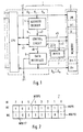
Im Blockschaltbild von Fig. 1 ist ein Ausführungsbeispiel einer Verriegelungsschaltung 1 im
Zusammenhang mit einem Prozessor 2 (Central Processing Unit = CPU) und einer
Speichereinrichtung 2 schematisch dargestellt. Die Verriegelungsschaltung, der Prozessor und die
zugehörige Speichereinrichtung bilden dabei vorzugsweise eine bauliche Einheit, indem sie
beispielsweise gemeinsam monolithisch integriert sind oder eine Hybridschaltung innerhalb eines
gemeinsamen Gehäuses bilden. Bei hohem Speicherbedarf kann es zweckmäßig sein, aus
Kostengründen die Speichereinrichtung nicht zusammen mit der CPU monolithisch zu integrieren,
sondern eine standardisierte Speichereinrichtung innerhalb einer Hybridschaltung oder eines
anderen Schaltungsverbundes zu verwenden. Somit ist die Verriegelungsschaltung 1 mit ihren
Funktionsblöcken 4, 5, 6, 7 bis auf den Funktionsblock 7 in der Regel eine Zusatzschaltung des
Prozessors 2. Die einzelnen Funktionsblöcke sind dabei ein Adressendekoder 4, eine logische
Verknüpfungseinrichtung 5, eine extern zugängliche Datenschnittstelle 6 und ein
Speicherschutzregister 7 (MPCR = Memory Protection Control Register), in dem die einzelnen
Zugangsberechtigungen festgehalten sind.1 is an embodiment of an
Der Programmablauf im Prozessor 2 teilt sich in Befehls- und Datenzyklen auf. Während eines
Befehlszyklus holt sich die CPU 2 den nächsten auszuführenden Befehl aus einer Programmfolge,
die in der CPU oder der Speichereinrichtung 3 gespeichert ist. Auf den Befehlszyklus folgt ein
oder mehrere Datenzyklen, in denen die CPU Daten holt oder Daten liefert. Vorzugsweise werden
dabei Daten aus der Speichereinrichtung 3 gelesen und dorthin zurückgeschrieben, wobei die Leseund
Schreiborte unterschiedlichen Bereichen Bi der Speichereinrichtung 3 zugeordnet sein
können. Das Lesen und Schreiben kann natürlich je nach dem vorausgehenden Befehl auch an
anderen, von der CPU adressierbaren Stellen erfolgen. Für die zu lösende Aufgabe ist jedoch
angenommen, daß die zu schützenden Daten nur die Daten der Speichereinrichtung 3 sind. Dabei
kann die Speichereinrichtung 3 in einzelne Bereiche B0, B1, ..Bi, ..Bn oder Segmente aufgeteilt
sein, die bezüglich einem unzulässigen Speicherzugriff von außen unterschiedlich zu behandeln
sind. So kann es erste Bereiche geben, die weder Lesen noch Schreiben zulassen, wobei der
Begriff Schreiben sich auf das Überschreiben mit neuen Daten oder auf das Löschen von
vorhandenen Daten bezieht. In zweiten Bereichen ist zwar das Lesen von Daten zugelassen, nicht
aber das Schreiben. In dritten Bereichen ist das Schreiben von Daten, nicht aber das Lesen
zugelassen. Und in vierten Bereichen gibt es keinerlei Beschränkung, also Lesen und Schreiben ist
in diesen Speicherbereichen ohne Beschränkung zugelassen. Welche Schutzfunktion den einzelnen
Speicherbereichen zukommt, ist im Speicherschutzregister 7, das im folgenden auch vereinfacht
als MPCR bezeichnet wird, festgehalten. Dieses Speicherschutzregister 7 befindet sich als
separates Register z.B. im Mikrokontroller oder vorzugsweise in der Speichereinrichtung 3. Die
letztere Realisierung ist besonders zweckmäßig, weil dann dieses Register MPCR 7 in einem
gegen Lesen und Schreiben geschützten Bereich untergebracht sein kann, wodurch die
Schutzfunktion für die gesamte Speichereinrichtung 3 nach der erstmaligen Programmierung ohne
besondere Vorkehrungen nicht mehr aufhebbar ist.The program flow in
Die Definition der einzelnen Speicherbereiche erfolgt im Adressendekoder 4, der aus den
zugeführten Adressen A0 ... Ai ... An je nach dem adressierten Speicherbereich Bi ein
Bereichssignal s2 (vergl. z.B. das Bereichssignal CEmemory i in Fig. 3) bildet, wobei die Größe der
Speicherbereiche über die Angaben der Bereichsgrenzen im Adressendekoder 4 vorgegeben ist. The definition of the individual memory areas takes place in the
Das Erkennen ob ein zulässiger oder unzulässiger Speicherzugriff vorliegt, erfolgt in der logischen
Verknüpfungseinrichtung 5, die interne und externe Signale s2, s3, s4 bzw. s1 logisch miteinander
verknüpft und aus dem Verknüpfungsergebnis einen zulässigen oder unzulässigen Zugriff erkennt.
Die grundsätzliche Zugangsregelung für den adressierten Speicherbereich Bi wird aus dem
Register 7 abgefragt.The detection of whether there is a permissible or impermissible memory access takes place in the
Bei einem zulässigen Speicherzugriff wird die Speichereinrichtung 3 vom Prozessor 2 mittels der
abgegebenen Steuersignale s3 bzw. s5 an der jeweiligen Adresse Ai gelesen oder geschrieben,
wobei die zu lesenden oder zu schreibenden Daten D0 ... Dn gegebenenfalls an der extern
zugänglichen Datenschnittstelle 6 als Daten d1 mitgelesen bzw. von dort aus in die
Speichereinrichtung 3 geschrieben werden können. Standardisierte Beispiele für derartige
Datenschnittstellen 6 sind unter der Bezeichnung "Test-Bus" oder "JTAG" (= Joint Test Action
Group) bekannt. Ihre Aktivierung erfolgt über ein entsprechendes externes Signal s1, das bei
Prozessoren und Mikrokontrollern meist sinngemäß mit "TEST" bzw. "JTAG" bezeichnet wird.
Die Verknüpfungseinrichtung 5 zwischen der CPU 2 und der Speichereinrichtung 3 ist in diesem
Fall gleichsam transparent und tritt nicht in Erscheinung, obwohl sie interne und externe Signale
s2, s3, s4 bzw. s1 miteinander verknüpft.In the event of a permissible memory access, the
Bei einem unzulässigen Speicherzugriff verhindert die Verknüpfungseinrichtung 5 die zum Lesen
oder Schreiben der Speichereinrichtung 3 erforderlichen Signale s5 oder sperrt zumindest die
extern zugängliche Datenschnittstelle 6 über ein Sperrsignal s6. Die Information über die
Zugangsregelung des jeweiligen Speicherbereiches frägt die Verknüpfungseinrichtung 5 mittels
des als Adresse dienenden Bereichssignals s2 vom Register 7 ab, das dann die jeweilige
Zugangsregelung über das Signal s4 zurückmeldet.In the event of an impermissible memory access, the linking
Eine grundsätzliche Bedingung für die Zugangssicherung ist, daß ein Zugriff auf die Speichereinrichtung
3 durch den Prozessor 2 im normalen Betrieb nicht behindert werden darf. Im
regulären Betriebsfall durchläuft die CPU 2 einen vollständigen Befehls-Datenzyklus, bei dem der
nächste Befehl und damit Programmschritt in die CPU geladen wird, der dann den oder die
zugehörigen Steuerbefehle, z.B. Lesen und/oder Schreiben, auf die zu schützende Speichereinrichtung
3 oder andere Datenquellen oder -senken auslöst. Das Erkennen dieses regulären Betriebszyklus
erfolgt beispielsweise durch die Verknüpfung eines Zustandssignals s3 mit einem
Bereichssignal s2. Als Zustandssignal s3 dient beispielsweise ein "Op-Code-Fetch"-Signal "OPC",
das mit dem Bereichssignal CEmemory i logisch verknüpft wird. Das "Op-Code-Fetch"-Signal
erzeugt die CPU immer dann, wenn ein Befehlszugriff erfolgt. Alle daraufhin folgenden
Datenzugriffe auf den gleichen Bereich Bi der Speichereinrichtung 3 bis zum nächsten "Op-Code-Fetch"-Signal
sollen ohne Beachtung der vorgesehenen Zugangsregelung zugelassen werden. Dies
gilt nicht, wenn für diesen Bereich eine Sperrinformation vorgesehen ist und über die
Datenschnittstelle 6 mittels eines "TEST"- oder "JTAG"-Signals ein Mitlesen oder Überschreiben
versucht wird.A basic condition for access security is that access to the
Ein irregulärer Speicherzugriff kann sich auch dadurch auszeichnen, daß er bestimmte
Widersprüche zwischen den Signalen s2, s3, s4 enthält. Dies wird ebenfalls überprüft. Zum Lesen
bzw. Schreiben erzeugt die CPU die bereits genannten Signale "RE" (=Read-Enable) bzw. "WE"
(=Write-Enable) und der Adressendekoder 4 mittels der von der CPU gebildeten Adresse Ai das
Speicher- Freigabesignal "CE" (=Chip-Enable) und/oder das Bereichssignal CEmemory i, die zur
Aktivierung der Speichereinrichtung 3 bei vielen segmentierten Speichertypen erforderlich sind.
Mittels einer Tabellendarstellung in Fig. 10 werden verschiedene Konstellationen zwischen den
Signalen und deren Auswirkung auf die Zugangsprüfung später deutlicher dargestellt.An irregular memory access can also be characterized in that it contains certain contradictions between the signals s2, s3, s4. This is also checked. For reading and writing, the CPU generates the already mentioned signals "RE" (= Read-Enable) or "WE" (= Write-Enable) and the
In Fig. 2 ist schematisch ein Beispiel für das Speicherschutzregister 7 (=MPCR) mit
angenommenem Inhalt dargestellt. Das MPCR-Register 7 in Fig. 3 enthält 16 Speicherplätze, die
jeweils im "0"- oder "1"-Zustand sind und insgesamt einem Datenwort mit 16 Bitstellen D0 bis
D15 entsprechen. Unter der Annahme, daß die Speichereinrichtung 3 in acht unterschiedliche
Speicherbereiche B0 bis B7 aufgeteilt ist, lassen sich somit aus dem 16-Bit-Datenwort zwei
getrennte 8-Bit-Bereiche bilden. Ein Bereich definiert die jeweilige Lese-Zugangsberechtigungen
und der andere die jeweiligen Schreib-Zugangsberechtigungen. Mit den ersten 8 Bit wird für jeden
der 8 Speicherbereiche B0 bis B7 eine positive oder negative Lese-Zugangsberechtigung MRP0
bis MRP7 und mit den zweiten 8 Bit eine positive oder negative Schreib-Zugangsberechtigung
MWP0 bis MWP7 festgelegt. Wenn als Datenumfang im Speicherschutzregister 7 weniger als 16
Bit zur Verfügung stehen, dann werden die 16 Zugangsberechtigungen in zwei getrennten
Registern gespeichert.2 schematically shows an example for the memory protection register 7 (= MPCR)
assumed content. The
Der für den jeweiligen Speicherbereich Bi gespeicherte Zustand "1" sperrt den Zugang und der
Zustand "0" gibt ihn frei. Die Wahl, welcher Zustand im MPCR-Register 7 den freien Zugang oder
die Sperrung definiert, ist an sich beliebig. Es muß jedoch sichergestellt sein, daß im unprogrammierten
Zustand alle Bits des MPCR-Registers 7 einen Freigabezustand aufweisen, ansonsten wäre
eine nachfolgende Programmierung des MPCR-Registers und der Speichereinrichtung 3 nicht
mehr möglich. Wenn durch die Technologie ein bestimmter Zustand für das unprogrammierte
Register 7 vorgegeben ist, dann wird dieser Zustand gegebenenfalls durch einen nachfolgenden
Inverter oder durch das Auslesen des invertierten Registerinhaltes korrigiert.The state "1" stored for the respective memory area Bi blocks access and
State "0" enables it. The choice of which state in the
In Fig. 3 ist schematisch ein Adressendekoder 4 dargestellt. Auf der einen Seite befinden sich die
Eingänge für die parallel zugeführten Adressenbits AD0 bis ADn und auf der anderen Seite die
Dekodierausgänge, die je nach dem dekodierten Speicherbereich B0 bis Bn jeweils ein
Bereichssignal CEmemory 0 bis CEmemory n abgeben. Ein globales Speicher-Freigabesignal CE
(=Chip-Enable), das den gesamten Speicherbereich B betrifft, wird an einem separaten Ausgang
abgegeben, wenn eine Adresse innerhalb des gesamten Adressenumfanges erkannt wird. Als
Zahlenbeispiel sind im Hexadezimalformat mögliche Bereiche B0, B1, B2, Bn angegeben. Für die
Eindeutigkeit der logischen Verknüpfung muß sichergestellt sein, daß jeweils nur ein einziges
Bereichssignal CEmemory i im Zustand "1" ist.An
Fig. 4 zeigt ein ähnliches Blockschaltbild wie Fig. 1. Als Speichereinrichtung 3 wird ein
segmentierter Speichertyp verwendet, dessen einzelnen Bereiche Bi gezielt mit einem Bereichs-Lesesignal
REmemory i oder einem Bereichs-Schreibsignal WEmemory i angesteuert werden müssen.
Zusätzlich ist nur ein globales Speicher-Freigabesignal CE erforderlich, das parallel an allen
Bereichen B0 bis Bn anliegt. Das Bereichssignal CEmemory i aus dem Adressendekoder 4 ist der
Verknüpfungseinrichtung 5.1 zugeführt, die dieses Signal mit den aus der CPU 2 stammenden
Signalen RE oder WE kombiniert und als zugehöriges Lese-Bereichssignal REmemory i oder
Schreib-Bereichssignal bzw. WEmemory i abgibt. Nur wenn diese Signale mit dem entsprechenden
Speicherbereich Bi übereinstimmen, kann dieser Bereich gelesen oder geschrieben werden. Dies
wird sichergestellt, indem nur ein einziger Bereich Bi mit dem Lese- oder Schreib-Bereichssignal
angesteuert wird. Die anderen Bereiche werden nicht angesteuert. Das Lese- oder Schreib-Bereichssignal
wird selbstverständlich nur abgegeben, wenn die Zugangsberechtigungsprüfung in
der Verknüpfungseinrichtung 5.1 mittels der Signale RE, WE, OPC, CEmemory i, MRPQi bzw.
MWPQi und der nicht dargestellten Signale TEST und JTAG einen zulässigen Zugang feststellt.
Bei einem unzulässigen Zugang, werden die Signale REmemory i oder WEmemory i von der
Verknüpfungseinrichtung 5.1 unterdrückt. Das globale Signal CE kann durch eine geeignete
Torschaltung gegebenenfalls zusätzlich unterdrückt werden.FIG. 4 shows a block diagram similar to FIG. 1. A segmented memory type is used as the
Das Blockschaltbild von Fig. 5 enthält wie Fig. 4 eine segmentierte Speichereinrichtung 3. Die
Bereichsauswahl erfolgt jedoch im Unterschied zu Fig. 4 nicht durch ein Bereichs-Lesesignal oder
ein Bereichs-Schreibsignal, sondern allein durch das Bereichssignal CEmemory i aus der logischen
Verknüpfungseinrichtung 5. Das Lese- oder Schreibsignal RE bzw. WE der CPU 2 ist dabei
einheitlich für die ganze Speichereinrichtung 3. Wie auch in Fig. 4 findet in der
Verknüpfungseinrichtung 5.2 eine Zugangsprüfung über die vorhandenen Signale statt. Bei einem
als unzulässig erkannten Zugriff wird das für den Zugriff in der Speichereinrichtung 3
erforderliche Bereichssignal CEmemory i gesperrt. Das globale Lese- oder Schreibsignal RE bzw.
WE kann durch eine geeignete Torschaltung gegebenenfalls zusätzlich unterdrückt werden. In Fig.
5 ist dies nicht der Fall, die Signale RE, WE sind daher unter Umgehung der
Verknüpfungseinrichtung 5.2 direkt der Speichereinrichtung 3 zugeführt.Like FIG. 4, the block diagram of FIG. 5 contains a
In Fig. 6 ist die logische Verknüpfungseinrichtung 5.1 von Fig. 4 für den Lesefall deutlicher
dargestellt. Damit die Speichereinrichtung 3 entsprechend dem Lesesignal RE von der CPU 2
gelesen werden kann, muß bei einem zulässigen Speicherzugriff die Verknüpfungseinrichtung ein
Bereichs-Lesesignal REmemory i der Speichereinrichtung zuführen. Vom Speicherschutzregister 7
ist lediglich eine einzige Speicherzelle 10 mit dem Symbol eines D-Flipflops dargestellt. Soll der
Inhalt MRPi der Speicherzelle 10 geändert werden, wird über die am D-Eingang angeschlossene
Datenleitung ein neues Datenbit Di in die Speicherzelle 10 geschrieben. Als Schreibtakt dient ein
Register-Schreibsignal WEMPCR aus der CPU 2. Ist das Speicherschutzregister 7 Teil eines Flash-Speichers,
dann ist zu berücksichtigen, daß der unprogrammierte Speicherzustand dem Logikpegel
"1" entspricht. Damit dieser Zustand in der nachgeschalteten Verknüpfungseinrichtung 5.1 nicht
als Sperrinformation interpretiert wird, wird der Inhalt MRPi der Speicherzelle 10 invertiert
ausgelesen. Im dargestellten D-Flipflop 10 entspricht dies einem Signalabgriff am invertierenden
Ausgang. Eine gespeicherte "1" wird somit zu "0" und umgekehrt.FIG. 6 shows the logical combination device 5.1 of FIG. 4 more clearly for the reading case. So that the
Die Prüfung ob ein Befehlszugriff oder eine Datenzugriff auf die Speichereinrichtung 3 vorliegt,
erfolgt über ein D-Flipflop 11. Es wird mit dem OP-Code-Fetch-Signal OPC am C-Eingang
getaktet und übernimmt damit das am D-Eingang vorhandene Speicher-Freigabesignal CE, sofern
dieses vorhanden ist. Das am Q-Ausgang abgegriffene Ausgangssignal dieses Flipflops 11 ist ein
Hilfssignal CEQ, das so lange den Zustand "1" aufweist, bis ein neuer Befehlszugriff OPC ohne
das Speicher-Freigabesignal CE signalisiert wird. Der "1"-Zustand des Hilfssignals CEQ
signalisiert somit, daß der letzte Befehlszugriff auf die Speichereinrichtung 3 erfolgte. Im Zustand
"0" bewirkt das Hilfssignal CEQ letztendlich eine Sperrung des erforderlichen Bereichs-Lesesignals
RE memory i. Über einen Reset-Eingang R kann das Flipflop 11 ebenfalls mittels eines
intern oder extern erzeugten Set-Resetsignals S/R in den Zustand "0" versetzt werden. Dies ist
beim Einschalten der Versorgungsspannung sinnvoll, weil in diesem instabilen Betriebszustand
kein Speicherzugriff erfolgen soll. Vorzugsweise wird für das D-Flipflop 11 ein Flipflop mit einem
"transparent-latch"-Verhalten verwendet, damit beim Startvorgang, solange also noch kein
Taktsignal OPC für den C-Eingang generiert wurde, der Q-Ausgang bereits das am D-Eingang
anliegende Speicher-Freigabesignal CE sieht und den nachfolgenden UND-Gattern 13, 14 als
aktuelle Information weiterleiten kann.A D flip-
Die Prüfung, ob das Speicherschutzregister 7 eine Sperr- oder eine Freigabeinformation als Inhalt
MRPi enthält, erfolgt durch ein D-Flipflop 12, dessen D-Eingang mit dem Datenausgang der
Speicherzelle 10 verbunden ist. Die jeweils gültige Information MRPi wird mit einem Register-Schreibsignal
REMPCR übernommen. Am Q-Ausgang wird es als Signal MRPQi zur weiteren
Verknüpfung abgegeben. Das Signal ist auf den Inhalt einer einzigen Speicherzelle 10 bezogen
und gilt nur für einen einzigen Speicherbereich Bi. Der Zustand "1" bzw. "0" dieses Signals
MRPQi entspricht einer Sperrwirkung bzw. einer Freigabewirkung. Die Sperrwirkung "1" wird
auch über das Set-Resetsignal S/R an einem Seteingang S des Flipflops 12 unabhängig von
anderen Signalen erzwungen, beispielsweise bei dem erwähnten Netzstart.The check as to whether the
Die wesentliche Prüfung, ob ein zulässiger oder unzulässiger Speicherzugriff vorliegt, erfolgt in
zwei UND-Gattern 13, 14 mit Mehrfacheingängen. Einige dieser, mit kleinen Kreisen markierten
Eingänge invertieren die zugeführten Signale vor der UND-Verknüpfung. Das erste UND-Gatter
13 ist im wesentlichen für diejenigen Fälle zuständig, in denen der Inhalt MRPi der zugeordneten
Speicherzelle 10 einer Freigabeinformation entspricht. Es muß dann nur noch überprüft werden, ob
der adressierte Speicherbereich CE memory i auch der adressierten Speicherzelle 10 zugeordnet ist
und ob auch tatsächlich ein Lesebefehl RE aus der CPU 2 vorliegt. Wenn alle drei Signale MRPQi,
CEQ und RE den richtigen Zustand "0", "1", "1" haben, dann wird für den zugehörigen Bereich Bi
mittels eines dem UND-Gatter 13 nachgeschalteten ODER-Gatters 15 das Bereichs-Lesesignal RE
memory i abgegeben.The essential check as to whether there is an allowable or inadmissible memory access is carried out in two AND
Das zweite UND-Gatter 14 ist im wesentlichen für diejenigen Fälle zuständig, in denen der Inhalt
MRPi der MPCR-Zelle 10 einer Sperrinformation entspricht, hier im Flash-Beispiel also eine "0"
aufweist Wie oben wird auch überprüft, ob der adressierte Speicherbereich CEi auch der
adressierten Speicherzelle 10 zugeordnet ist und ob ein von der CPU 2 generierter Lesebefehl RE
vorliegt. Sind alle Bedingungen erfüllt, bedeutet dies, daß ein zulässiger Datenzugriff von der CPU
2 innerhalb eines vollständigen Befehls-und-Datenzyklus auf den gleichen Speicherbereich Bi
vorliegt. Dies gilt indessen nur dann, wenn nicht über die externen Signale JTAG oder TEST ein
Mitlesen der Daten versucht wird. Daher wird das Nichtvorhandensein dieser Signale ebenfalls in
die UND-Verknüpfung durch das Gatter 14 einbezogen. Hierzu werden die negierenden Eingänge
verwendet. Mittels der UND-Verknüpfung gibt das zweite UND-Gatter 14 über das
nachgeschaltete ODER-Gatter 15 nur dann ein Bereichs-Lesesignal RE memory i ab, wenn die
Signale MRPQi, CEQ, RE, JTAG, TEST und CEi die logischen Pegel "1", "1", "1", "0", "0" und
"1" aufweisen. In Fig. 6 sind zur verständlichen Darstellung der logischen Verknüpfungen die
einzelnen Funktionsblöcke wie Flipflopstufen, UND- oder ODER-Gatter dargestellt. Diese können
selbstverständlich ganz oder teilweise durch eine entsprechende andere Hard- oder Software
ersetzt sein, wobei auch die Verknüpfung eine andere sein kann, sofern das Ergebnis identisch ist.The second AND
Die obige Funktionsbeschreibung der Verknüpfungseinrichtung 5.1 von Fig. 6 betrifft den Lesefall. Für den Schreibfall gilt indessen die gleiche Schaltung, nur sind einige Signale durch die entsprechenden Schreibsignale zu ersetzen. In der Darstellung stehen diese Signale MWPI, MWPQi, WE und WE memory i in Klammern bei den zu ersetzenden Signalen.The above functional description of the link device 5.1 of FIG. 6 relates to the reading case. However, the same circuit applies to the write case, only some signals have to be replaced by the corresponding write signals. These signals MWPI, MWPQi, WE and WE memory i are shown in parentheses in the representation of the signals to be replaced.
In Fig. 7 ist als Beispiel ein Teil der Verknüpfungseinrichtung 5.2 von Fig. 5 als Blockschaltbild
mit den einzelnen Logikeinheiten dargestellt. Die Schaltung zeigt die Logikeinheiten und Signale,
die einem einzigen Speicherbereich Bi zugeordnet sind. Für jeden Speicherbereich ist eine gleiche
Anordnung erforderlich. Die Schaltung liefert ein Bereichssignal CEmemory i, wenn der Zugriff auf
die nicht dargestellte Speichereinrichtung 3 zulässig ist. Die Verknüpfungseinrichtung 5.2 ist dabei
der beschriebenen Verknüpfungseinrichtung 5.1 von Fig. 6 sehr ähnlich und enthält zwei MPCR-Speicherzellen
20 bzw. 21 für die Lese-Zugangsinformation MRPi bzw. die Schreib-Zuganginformation
MWRPi. Das Hilfssignal CEQ wird wieder durch ein "transparentes" D-Flipflop
22 gebildet. Die Abfrage der Lese-Zugangsinformation aus der Zelle 20 erfolgt durch ein
D-Flipflop 23 und der Schreib-Zugangsinformation aus der Zelle 21 durch ein D-Flipflop 24, die
als Ausgangsignale ein MRPQ-Lese- bzw. MWPQ-Schreibsignal liefern.FIG. 7 shows, as an example, part of the logic device 5.2 from FIG. 5 as a block diagram with the individual logic units. The circuit shows the logic units and signals which are assigned to a single memory area Bi. The same arrangement is required for each memory area. The circuit supplies an area signal CE memory i when access to the
Die Ermittlung der Lese-Zugangsberechtigung erfolgt im wesentlichen mittels der beiden UND-Gatter
25, 26 und die Ermittlung der Schreib-Zugangsberechtigung mittels der beiden UND-Gatter
27, 28. Alle UND-Gatter eines Bereiches Bi sind ausgangsseitig mittels eines ODER-Gatters 29
zusammengeführt, das ein Bereichssignal CEmemory i abgibt, wenn wenigstens eines der vier UND-Gatter
den Logikzustand "1" aufweist. Die Unterscheidung des Lese- oder Schreibbetriebs kann
über das Lese- und Schreibsignal RE, WE erfolgen. Beide Signale können jedoch wie in Fig. 7
auch als ein einziges Lese-Schreibsignal R/W zusammengefaßt werden, wobei der logische Pegel
"0" Lesen und der logische Pegel "1" Schreiben bedeutet. Die UND-Gatter 25, 26, 27, 28 haben
jeweils mindestens drei Eingänge, wobei invertierende Eingänge in Fig. 7 mit einem kleinen Kreis
gekennzeichnet sind. Die Zuordnung der einzelnen Signale zu den einzelnen UND-Gattern ergibt
sich ohne weiteres aus der Zeichnung. Selbstverständlich sind die logischen Verknüpfungen der
digitalen Signale der Verknüpfungseinrichtung 5.2 ganz oder teilweise auch über eine
entsprechende Hard- oder Software realisierbar. Sofern das Ergebnis gleich bleibt, kann auch die
Logik eine andere sein.The read access authorization is essentially determined by means of the two AND
In Fig. 8 sind im Zeitdiagramm der zeitliche Verlauf einiger Signale der Verknüpfungseinrichtung beim Lesen dargestellt. Die dabei zugrunde gelegte Verknüpfungseinrichtung entspricht etwa der Verknüpfungseinrichtung 5.1 von Fig. 6 mit freigegebenem Speicherzugriff. Die erste Zeile zeigt ein kombiniertes Lese-Schreibsignal R/W, das in dem einen Logikzustand Lesen und in dem anderen Schreiben bedeutet. In den hell dargestellten Bereichen ist der Zustand des R/W-Signals gültig oder definiert (=valid), in den schraffierten Bereichen kann er beliebig sein. Die zugehörigen Takte T1, T2, T3 und T4 entsprechen den äquidistanten Bereichen des R/W-Signals. Das eigentliche Taktsignal ist nicht dargestellt. Statt der dargestellten Signale können selbstverständlich auch die invertierten oder inversen Signale verwendet werden, sofern die Logik entsprechend angepaßt wird.8 shows the time course of some signals of the linking device in the time diagram shown while reading. The linking device used here corresponds approximately to that Linking device 5.1 of FIG. 6 with released memory access. The first line shows a combined read / write signal R / W, which in the one logic state read and in the other writing means. The state of the R / W signal is in the bright areas valid or defined (= valid), it can be any in the hatched areas. The associated clocks T1, T2, T3 and T4 correspond to the equidistant areas of the R / W signal. The actual clock signal is not shown. Instead of the signals shown can of course, the inverted or inverse signals can also be used, provided the logic is adjusted accordingly.
Im ersten Takt T1 findet ein Befehlszugriff von der CPU 2 auf die Speichereinrichtung 3 statt.
Dem entspricht das OP-Code-Fetch-Signal OPC in Zeile 2 und das Speicher-Bereichssignal
CEmemory i in Zeile 3.In the first cycle T1, command access from the
Dem Befehlszugriff folgt im zweiten Takt T2 ein Lesezugriff auf den gleichen Speicherbereich Bi.
Dies wird durch das Speicher-Bereichssignal CEmemory i im Takt 2 signalisiert. Ein OPC-Signal
wird nicht erzeugt, da es sich um einen Datenzugriff handelt. Andererseits gehört der Datenzugriff
zu einem vollständigen Befehls-Datenzyklus auf den gleichen Speicherbereich Bi. Dies zeigt das
Signal CEQ in der vierten Zeile an, das im ersten Takt T1 in den "1"-Zustand gesetzt wird erst
wieder im dritten Takt T3 durch das neue OPC-Signal zurückgesetzt wird.The command access is followed in the second cycle T2 by a read access to the same memory area Bi. This is signaled by the memory area signal CE memory i in
Im dritten Takt T3 beginnt ein neuer Befehls-Datenzyklus, der erstreckt sich jedoch nicht auf den vorherigen Speicherbereich Bi, sondern auf einen anderen Speicherbereich oder eine andere Datenquelle oder Datensenke. A new command data cycle begins in the third cycle T3, but does not extend to that previous memory area Bi, but to another memory area or another Data source or sink.
Im Takt 4 wird angenommen daß in dem aktuellen Befehls-Datenzyklus irgendwie ein Zugriff auf
den Speicherbereich Bi ausgelöst wird. Dem entspricht das Bereichssignal CEmemory i zum
Zeitpunkt T4, ohne daß gleichzeitig das CEQ-Signal gesetzt ist. Ein derartiger Zugriff kann
beispielsweise über einen nicht dargestellten TJAG-Befehl ausgelöst werden.In
Die ersten vier Zeilen haben noch nichts mit einer positiven oder negativen Zugangsberechtigung zu tun, sondern mit diesen Signalen R/W, OPC, CEmemory i und CEQ wird der aktuelle Zustand des ganzen Systems beschrieben.The first four lines have nothing to do with a positive or negative access authorization, but with these signals R / W, OPC, CE memory i and CEQ the current status of the entire system is described.
In der fünften Zeile ist das Lese-Zugangsberechtigungssignal MRPQi für den Bereich Bi angegeben. Es hat während des gesamten Zeitablaufs den logischen Pegel "0" und bedeutet daher einen freien Lesezugang auf den Speicherbereich Bi.In the fifth line is the read access authorization signal MRPQi for the area Bi specified. It has the logic level "0" during the entire time period and therefore means free read access to the memory area Bi.
Die sechste Zeile zeigt den zeitlichen Verlauf des globalen Lesesignals RE, das immer dann von
der CPU 2 aktiviert wird, wenn sie Befehle oder Daten aus der Speichereinrichtung 3 abfrägt, also
während des ersten, zweiten und vierten Taktes. Der Befehlsabruf im dritten Takt T3 löst keinen
Lesebefehl RE aus, weil der mit dem zweiten OP-Code-Fetch-Signal gestartete Befehls-Datenzyklus
nicht auf die Speichereinrichtung 3 zugreift.The sixth line shows the temporal course of the global read signal RE, which is always from
the
Die sechste Zeile zeigt schließlich das resultierende Lese-Bereichssignal REmemory i, das bis auf eine kleine Zeitverzögerung infolge der Signallaufzeit durch die logischen Schaltstufen identisch mit dem Lesesignal RE ist, weil eine Sperrwirkung für diesen Speicherbereich Bi für das Lesen nicht vorgesehen ist. Damit die gegenseitige Abhängigkeit der Signale im Zeitdiagramm erkennbar wird, enthält Fig. 8 und Fig. 9 im Bereich einiger Signalwechsel Pfeile, um die auslösenden und resultierenden Signalwechsel und Signalzustände zu kennzeichnen.The sixth line finally shows the resulting read area signal RE memory i , which is identical to the read signal RE except for a small time delay due to the signal delay by the logic switching stages, because a blocking effect for this memory area Bi is not provided for reading. So that the interdependency of the signals can be seen in the time diagram, FIGS. 8 and 9 contain arrows in the area of some signal changes in order to identify the triggering and resulting signal changes and signal states.
Das Zeitdiagramm von Fig. 9 ist ähnlich zum Zeitdiagramm von Fig. 8. Der Hauptunterschied
besteht darin, daß die Lese-Zugangsberechtigung MRPQi in Zeile 5 den logischen Zustand "1"
aufweist und damit den Speicherbereich Bi für unerlaubte Lesezugriffe sperrt.The timing diagram of FIG. 9 is similar to the timing diagram of FIG. 8. The main difference
consists in the read access authorization MRPQi in
Damit ein Vergleich stattfinden kann, sind in den vier Takten T1, T2, T3 und T4 des Zeitdiagramms von Fig. 9 die selben Vorgänge beschrieben wie in Fig. 8. Die vier ersten Zeilen mit den Signalen R/W, OPC, CEmemory i und CEQ sind daher in Fig. 8 und Fig. 9 identisch. Erst mit dem MRPQi-Signal der fünften Zeile wird das Zeitdiagramm unterschiedlich.In order for a comparison to take place, the same processes as in FIG. 8 are described in the four clocks T1, T2, T3 and T4 in the time diagram of FIG. 9. The first four lines with the signals R / W, OPC, CE memory i and CEQ are therefore identical in FIGS. 8 and 9. Only with the MRPQi signal of the fifth line does the timing diagram differ.
Der erste und zweite Takt T1, T2 umfaßt einen regulären Befehls-Datenzyklus auf den gleichen
Speicherbereich Bi. Der von der CPU 2 ausgelöste Lesevorgang im ersten und zweiten Takt T1,
T2 soll aber trotz der Sperrinformation unbehindert ablaufen. Die resultierenden Lese-Bereichssignale
REmemory i im ersten und zweiten Takt werden somit wie in Fig. 8 gebildet Anders
sieht es bei dem Speicherzugriffsversuch im vierten Takt T4 aus. Daß es sich nicht um einen
regulären Zugriff handelt ergibt sich aus dem "0"-Pegel des Hilfssignals CEQ. Dieses Signal in
Verbindung mit dem Sperrsignal MRPQi sperrt das Bereichs-Lesesignal REmemory i, so daß ein
Lesen im Bereich Bi trotz richtigem Bereichssignal CEmemory i nicht möglich ist.The first and second clock T1, T2 comprise a regular command data cycle on the same memory area Bi. The reading process triggered by the
Fig. 10 zeigt in Tabellenform die Funktionsweise der Verknüpfungseinrichtung 5.1 von Fig. 6. Die einzelnen Zeilen zeigen den jeweiligen Logikzustand mit "0"- und "1" der angegebenen Signale. Die einzelnen Spalten enthalten dabei nacheinander folgende Signale: Die bereichsbezogene Lese-Zugangsberechtigung MRPi, das JTAG-Signal, das TEST-Signal, das Speicher-Bereichssignal CEmemory i, das globale Lesesignal RE und schließlich das Bereichs-Lesessignal REmemory i. Die letzte Spalte zeigt die aus den vorausgehenden Signalen resultierende Aktion: "Lesen" oder keine Leseaktion.10 shows in table form the mode of operation of the link device 5.1 from FIG. 6. The individual lines show the respective logic state with “0” and “1” of the signals indicated. The individual columns contain the following signals in succession: the area-related read access authorization MRPi, the JTAG signal, the TEST signal, the memory area signal CE memory i , the global read signal RE and finally the area read signal RE memory i. The last column shows the action resulting from the previous signals: "Read" or no read action.
In den ersten drei Zeilen hat die Lese-Zugangsberechtigung MRPQi den Zustand "0" und dies
bedeutet, daß der zugehörige Speicherbereich Bi für das Lesen nicht gesperrt sein soll, sondern
einen freien Zugriff ermöglicht. Der Zustand der Signale CEQ, JTAG und TEST ist für diese
Zugangsberechtigung beliebig. Die Verknüpfungseinrichtung überprüft jedoch, ob ein
Widerspruch zwischen dem Bereichssignal CEmemory i und dem globalen Lesesignal RE vorliegt. So
wird in Zeile 1 nicht gelesen, weil das Signal RE inaktiv ist. In Zeile 2 wird nicht gelesen, weil das
Bereichssignal CEmemory i inaktiv ist. Erst in der 3. Zeile ist das Bereichssignal und das globale
Lesesignal gesetzt, so daß das Bereichs-Lesesignal REmemory i mit dem Zustand "1" abgegeben wird,
und somit die Speichereinrichtung 3 an der adressierten Stelle gelesen wird. Die logischen
Verknüpfungen der Zeilen 1, 2 und 3 finden gemäß Fig. 6 in dem UND-Gatter 13 statt.In the first three lines, the read access authorization MRPQ i has the state "0" and this means that the associated memory area B i should not be blocked for reading, but rather allows free access. The status of the signals CEQ, JTAG and TEST is arbitrary for this access authorization. However, the linking device checks whether there is a contradiction between the area signal CE memory i and the global read signal RE. So
In den Zeilen 4 bis 9 ist der Leseschutz aktiv und entsprechend befindet sich das Signal MRBQi im
"1"- Zustand. Die logische Verknüpfung der Signale in diesen Zeilen muß so ausgebildet sein, daß
jeder Leseversuch auf den zugehörigen Speicherbereich Bi unterbunden wird, es sei denn, es
handelt sich um den oben beschriebenen regulären Zugriff, bei dem jedoch diese Signale JTAG
und TEST inaktiv, also im Zustand "0" sein müssen - letzteres zeigt Zeile 9. Daß es sich bei Zeile
4 nicht um einen regulären Zugriff handelt, geht beispielsweise schon daraus hervor, daß das
globale Schreibsignal RE inaktiv ist. In Zeile 5 handelt es sich ebenfalls nicht um einen regulären
Zugriff, weil das Bereichssignal CE memory i für diesen Bereich Bi nicht gesetzt ist, weil die vom
Prozessor ausgegebene Adresse nicht auf diesen Speicherbereich Bi verweist. In Zeile 6 wird der
Zugriff verweigert, weil ein Widerspruch zwischen dem Hilfssignal CEQ und dem Bereichssignal
CE memory i vorliegt. Auf irgendeine Weise ist zwar ein richtiges Bereichssignal vorhanden, der
Prozessor hat jedoch eine Adresse ausgegeben, die überhaupt nicht mit der Speichereinrichtung 3
verknüpft ist. Ein unzutreffendes Hilfssignal CEQ mit dem Zustand "0" liegt auch in Zeile 4 und 5
vor und kann daher auch dort in die Erkennung des irregulären Betriebszustandes einbezogen
werden.In
In den Zeilen 7 bis 9 hat das Hilfssignal CEQ den Zustand "1" und läßt somit keinen Widerspruch
zum Gesamtspeicherbereich B erkennen. In Zeile 7 wird indessen der Lesezugriff verweigert, weil
das Lesesignal RE inaktiv ist. In Zeile 8 wird der Lesezugriff verweigert, weil das Bereichssignal
CEmemory i inaktiv ist.In
Zeile 9 erlaubt wie bereits erwähnt das Lesen, obwohl der Speicherbereich Bi gesperrt ist, weil ein
regulärer Speicherzugriff vom Prozessor 2 vorliegt. Sowie jedoch in diesem Zustand das
unerlaubte Mitlesen über die Signale JTAG oder TEST versucht wird, wird das Lesen
unterbunden. Diese beiden Signale müssen sich daher im inaktiven Zustand befinden, der hier
durch "0" gekennzeichnet ist. Dies geht auch aus den Zeilen 10 und 11 hervor, die bei einem
gesperrten Speicherbereich das Lesen unterbinden, wenn eines oder beide dieser Signale aktiv
sind. Der logische Zustand der übrigen Signale ist dabei beliebig. Die in der Tabelle dargestellte
Speicheraktion in der letzten Spalte entspricht dem Zustand des Bereichs-Lesesignals REmemory i.
Die logischen Verknüpfungen der Zeilen 4 bis 11 lassen sich durch eine UND-Verknüpfung
realisieren. Dies entspricht dem UND-Gatter 14 von Fig. 6. As already mentioned,
- 11
- Verriegelungsschaltunglocking circuit
- 22
- Prozessor(einheit) (CPU=Central Processor Unit)Processor (unit) (CPU = Central Processor Unit)
- 33
- Speichereinrichtungmemory device
- 44
- Adressendekoderaddress decoder
- 55
- (logische) Verknüpfungseinrichtung(Logical) linking device
- 66
- extern zugängliche Datenschnittstelleexternally accessible data interface
- 77
- Speicherschutzregister (MPCR= Memory Protection Control Register)Memory protection register (MPCR)
- 1010
- (MPCR)-Speicherzelle(MPCR) memory
- 1111
- D-FlipflopD flip-flop
- 1212
- D-FlipflopD flip-flop
- 1313
- erstes UND-Gatterfirst AND gate
- 1414
- zweites UND-Gattersecond AND gate
- 1515
- ODER-GatterOR gate
- 2222
- D-Flipflop (transparent latch)D flip-flop (transparent latch)
- 2929
- ODER-GatterOR gate
- 20, 2120, 21
- (MCPR)-Speicherzelle(MCPR) memory
- 23, 2423, 24
- D-FlipflopD flip-flop
- 25, 26, 27, 2825, 26, 27, 28
- UND-GatterAND gate
- 5.1 5.25.1 5.2
- weitere Verknüpfungseinrichtungenfurther linking devices
- AD0, AD1, ADnAD0, AD1, ADn
- Eingang für AdressenbusAddress bus input
- Ai, A0, A1, AnAi, A0, A1, An
- Adressenaddresses
- Bi, B0, B1, B2Bi, B0, B1, B2
- Speicherbereichstorage area
- CC
- Takteingang / C-EingangClock input / C input
- CECE
- (globales) Speicher-Freigabesignal (=Chip Enable)(global) memory enable signal (= chip enable)
- CE memory iCE memory i
- SpeicherbereichssignalStorage area signal
- CEQCEQ
- Hilfssignalauxiliary signal
- D iRTo you
- Datenstelle (für Lese-Zugangsberechtigung)Data center (for read access authorization)
- D iWD iW
- Datenstelle (für Schreib-Zugangsberechtigung)Data center (for write access authorization)
- D(i, 0, 1, n)D (i, 0, 1, n)
- DatenData
- d1d1
- Schnittstellen-AusgangssignalInterface output signal
- JTAGJTAG
- Zugangssignal zu Schnittstelle JTAGAccess signal to the JTAG interface
- MRP(i, 0, 1,2)MRP (i, 0, 1.2)
- Lese-ZugangsberechtigungRead access authorization
- MWP(i, 0, 1, 2)MWP (i, 0, 1, 2)
- Schreib-Zugangsberechtigung Write access authorization
- OPCOPC
- Befehlszyklus-Zustandssignal (=Op-Code-Fetch)Command cycle status signal (= op code fetch)
- RR
- Reseteingangreset input
- R/WR / W
- kombiniertes Lese-Schreibsignalcombined read / write signal
- RERE
- Lesesignal (=Read Enable)Read signal (= Read Enable)
- RE memory iRE memory i
- Bereichs-LesesignalArea read signal
- RE MPCRRE MPCR
- Register-LesesignalRegister read signal
- SS
- Seteingangset input
- S/RS / R
- Set-ResetsignalSet-reset signal
- s1s1
- externe Signaleexternal signals
- s2, s3, s4s2, s3, s4
- interne Signaleinternal signals
- TT
- Zeittime
- T1, T2, T3, T4T1, T2, T3, T4
- 1. 2. 3. 4. Takt1st 2nd 3rd 4th bar
- TESTTEST
- Zugangssignal zu Schnittstelle TESTAccess signal to the TEST interface
- WEWE
- Schreibsignal (=Write Enable)Write signal (= Write Enable)
- WE memory iWE memory i
- Bereichs-SchreibsignalArea write signal
- WE MPCRWE MPCR
- Register-SchreibsignalRegister write signal
Claims (11)
Priority Applications (3)
| Application Number | Priority Date | Filing Date | Title |
|---|---|---|---|
| EP01108711A EP1248200A1 (en) | 2001-04-06 | 2001-04-06 | Locking circuit for preventing unauthorized access to a memory of a processor |
| JP2002105364A JP2002358237A (en) | 2001-04-06 | 2002-04-08 | Protection circuit for preventing access without privilege to memory device of processor |
| US10/117,975 US7054121B2 (en) | 2001-04-06 | 2002-04-08 | Protection circuit for preventing unauthorized access to the memory device of a processor |
Applications Claiming Priority (1)
| Application Number | Priority Date | Filing Date | Title |
|---|---|---|---|
| EP01108711A EP1248200A1 (en) | 2001-04-06 | 2001-04-06 | Locking circuit for preventing unauthorized access to a memory of a processor |
Publications (1)
| Publication Number | Publication Date |
|---|---|
| EP1248200A1 true EP1248200A1 (en) | 2002-10-09 |
Family
ID=8177073
Family Applications (1)
| Application Number | Title | Priority Date | Filing Date |
|---|---|---|---|
| EP01108711A Withdrawn EP1248200A1 (en) | 2001-04-06 | 2001-04-06 | Locking circuit for preventing unauthorized access to a memory of a processor |
Country Status (3)
| Country | Link |
|---|---|
| US (1) | US7054121B2 (en) |
| EP (1) | EP1248200A1 (en) |
| JP (1) | JP2002358237A (en) |
Families Citing this family (11)
| Publication number | Priority date | Publication date | Assignee | Title |
|---|---|---|---|---|
| US7185249B2 (en) * | 2002-04-30 | 2007-02-27 | Freescale Semiconductor, Inc. | Method and apparatus for secure scan testing |
| US7320642B2 (en) * | 2002-09-06 | 2008-01-22 | Wms Gaming Inc. | Security of gaming software |
| DE10347259B4 (en) * | 2003-10-08 | 2013-10-31 | Entropic Communications, Inc. | Method for synchronizing a circuit arrangement upon receipt of a modulated signal |
| US7386774B1 (en) * | 2004-02-26 | 2008-06-10 | Integrated Device Technology, Inc. | Memory unit with controller managing memory access through JTAG and CPU interfaces |
| GB2442023B (en) * | 2006-09-13 | 2011-03-02 | Advanced Risc Mach Ltd | Memory access security management |
| JP5081761B2 (en) * | 2008-08-05 | 2012-11-28 | 富士通株式会社 | Archive device, unauthorized access detection method, and unauthorized access detection program |
| CN103064798B (en) * | 2011-10-19 | 2016-02-03 | 国基电子(上海)有限公司 | Electronic equipment |
| TWI443518B (en) | 2011-10-19 | 2014-07-01 | Hon Hai Prec Ind Co Ltd | Electric device |
| US10540524B2 (en) | 2014-12-31 | 2020-01-21 | Mcafee, Llc | Memory access protection using processor transactional memory support |
| WO2018230280A1 (en) * | 2017-06-14 | 2018-12-20 | 住友電気工業株式会社 | External communication system for vehicle, communication control method, and communication control program |
| US20240086556A1 (en) | 2022-09-12 | 2024-03-14 | Idaho Scientific Llc | Computing data and instructions at immutable points |
Citations (5)
| Publication number | Priority date | Publication date | Assignee | Title |
|---|---|---|---|---|
| US4523271A (en) * | 1982-06-22 | 1985-06-11 | Levien Raphael L | Software protection method and apparatus |
| US4796235A (en) * | 1987-07-22 | 1989-01-03 | Motorola, Inc. | Write protect mechanism for non-volatile memory |
| US5557743A (en) * | 1994-04-05 | 1996-09-17 | Motorola, Inc. | Protection circuit for a microprocessor |
| US5657444A (en) * | 1995-08-03 | 1997-08-12 | National Semiconductor Corporation | Microprocessor with secure programmable read only memory circuit |
| US5974500A (en) * | 1997-11-14 | 1999-10-26 | Atmel Corporation | Memory device having programmable access protection and method of operating the same |
Family Cites Families (2)
| Publication number | Priority date | Publication date | Assignee | Title |
|---|---|---|---|---|
| US6397301B1 (en) * | 1999-12-29 | 2002-05-28 | Intel Corporation | Preventing access to secure area of a cache |
| US6665782B2 (en) * | 2001-08-16 | 2003-12-16 | International Business Machines Corporation | Method and apparatus for preventing unauthorized access of memory devices |
-
2001
- 2001-04-06 EP EP01108711A patent/EP1248200A1/en not_active Withdrawn
-
2002
- 2002-04-08 US US10/117,975 patent/US7054121B2/en not_active Expired - Lifetime
- 2002-04-08 JP JP2002105364A patent/JP2002358237A/en active Pending
Patent Citations (5)
| Publication number | Priority date | Publication date | Assignee | Title |
|---|---|---|---|---|
| US4523271A (en) * | 1982-06-22 | 1985-06-11 | Levien Raphael L | Software protection method and apparatus |
| US4796235A (en) * | 1987-07-22 | 1989-01-03 | Motorola, Inc. | Write protect mechanism for non-volatile memory |
| US5557743A (en) * | 1994-04-05 | 1996-09-17 | Motorola, Inc. | Protection circuit for a microprocessor |
| US5657444A (en) * | 1995-08-03 | 1997-08-12 | National Semiconductor Corporation | Microprocessor with secure programmable read only memory circuit |
| US5974500A (en) * | 1997-11-14 | 1999-10-26 | Atmel Corporation | Memory device having programmable access protection and method of operating the same |
Also Published As
| Publication number | Publication date |
|---|---|
| US7054121B2 (en) | 2006-05-30 |
| JP2002358237A (en) | 2002-12-13 |
| US20020166034A1 (en) | 2002-11-07 |
Similar Documents
| Publication | Publication Date | Title |
|---|---|---|
| EP1276033B1 (en) | Memory device with data protection in a processor | |
| DE2954731C2 (en) | Monolithic microprocessor | |
| DE3048365C2 (en) | ||
| EP0128362B1 (en) | Circuit arrangement comprising a memory and an access control unit | |
| EP1089219B1 (en) | Method for protecting a data memory | |
| EP0766211A2 (en) | Multifunctional IC-card | |
| DE2749850B2 (en) | Hybrid semiconductor memory with associative page addressing, page exchange and control on the chip | |
| EP0224639B1 (en) | Method to control the memory access of an ic card and implementing device | |
| EP1248200A1 (en) | Locking circuit for preventing unauthorized access to a memory of a processor | |
| DE19963208B4 (en) | A method of tampering with a programmable memory device of a digital controller | |
| EP1262856B1 (en) | Program controlled unit | |
| DE102005022019A1 (en) | Secure processing of data | |
| EP0935214B1 (en) | Smart card with integrated circuit | |
| DE19954407A1 (en) | Method for directly calling a function by means of a software module by a processor with a memory management unit (MMU) | |
| DE1499742A1 (en) | Controllable memory access device for memory devices of data processing systems with multi-program processing | |
| DE19623145B4 (en) | Method for operating a control device with a memory device programmable via a programming device | |
| DE19901829A1 (en) | Circuit arrangement for electronic data processing | |
| EP1563358B1 (en) | Method for the secure checking of a memory region of a microcontroller in a control device and control device with a protected mikrocontroller | |
| DE4227784A1 (en) | COMPUTER SYSTEM AND METHOD FOR REMOVING A PAGE ERROR | |
| DE102021131424A1 (en) | METHODS AND SYSTEMS FOR SESSION-BASED AND SECURE ACCESS CONTROL TO A DATA STORAGE SYSTEM | |
| DE19612439C2 (en) | Semiconductor memory device | |
| EP0214390A1 (en) | Release method and device for a controlled-access user memory | |
| DE1524183C (en) | ||
| DE10303452B4 (en) | Method for controlling the interruption and / or recording of execution data of a program in a microcontroller and microcontroller with an arrangement for carrying out the method | |
| DE4340027A1 (en) | Write protection for EEPROM in electronic control system |
Legal Events
| Date | Code | Title | Description |
|---|---|---|---|
| PUAI | Public reference made under article 153(3) epc to a published international application that has entered the european phase |
Free format text: ORIGINAL CODE: 0009012 |
|
| AK | Designated contracting states |
Kind code of ref document: A1 Designated state(s): AT BE CH CY DE DK ES FI FR GB GR IE IT LI LU MC NL PT SE TR |
|
| AX | Request for extension of the european patent |
Free format text: AL;LT;LV;MK;RO;SI |
|
| 17P | Request for examination filed |
Effective date: 20030409 |
|
| AKX | Designation fees paid |
Designated state(s): DE FR GB IT NL |
|
| 17Q | First examination report despatched |
Effective date: 20060913 |
|
| 17Q | First examination report despatched |
Effective date: 20060913 |
|
| STAA | Information on the status of an ep patent application or granted ep patent |
Free format text: STATUS: THE APPLICATION IS DEEMED TO BE WITHDRAWN |
|
| 18D | Application deemed to be withdrawn |
Effective date: 20071023 |