EP1220077A2 - Data processing apparatus and memory card using the same - Google Patents
Data processing apparatus and memory card using the same Download PDFInfo
- Publication number
- EP1220077A2 EP1220077A2 EP01130510A EP01130510A EP1220077A2 EP 1220077 A2 EP1220077 A2 EP 1220077A2 EP 01130510 A EP01130510 A EP 01130510A EP 01130510 A EP01130510 A EP 01130510A EP 1220077 A2 EP1220077 A2 EP 1220077A2
- Authority
- EP
- European Patent Office
- Prior art keywords
- data
- control signal
- read
- write
- circuit
- Prior art date
- Legal status (The legal status is an assumption and is not a legal conclusion. Google has not performed a legal analysis and makes no representation as to the accuracy of the status listed.)
- Granted
Links
- 230000005540 biological transmission Effects 0.000 description 9
- 230000000875 corresponding effect Effects 0.000 description 9
- 238000010586 diagram Methods 0.000 description 9
- 230000002093 peripheral effect Effects 0.000 description 5
- 230000000694 effects Effects 0.000 description 2
- 238000000034 method Methods 0.000 description 2
- 230000002596 correlated effect Effects 0.000 description 1
- 230000006870 function Effects 0.000 description 1
- 230000004044 response Effects 0.000 description 1
Images


Classifications
-
- G—PHYSICS
- G06—COMPUTING; CALCULATING OR COUNTING
- G06F—ELECTRIC DIGITAL DATA PROCESSING
- G06F12/00—Accessing, addressing or allocating within memory systems or architectures
- G06F12/14—Protection against unauthorised use of memory or access to memory
-
- G—PHYSICS
- G06—COMPUTING; CALCULATING OR COUNTING
- G06F—ELECTRIC DIGITAL DATA PROCESSING
- G06F13/00—Interconnection of, or transfer of information or other signals between, memories, input/output devices or central processing units
- G06F13/38—Information transfer, e.g. on bus
- G06F13/42—Bus transfer protocol, e.g. handshake; Synchronisation
- G06F13/4204—Bus transfer protocol, e.g. handshake; Synchronisation on a parallel bus
- G06F13/4234—Bus transfer protocol, e.g. handshake; Synchronisation on a parallel bus being a memory bus
- G06F13/4239—Bus transfer protocol, e.g. handshake; Synchronisation on a parallel bus being a memory bus with asynchronous protocol
Definitions
- a memory card which comprises: an operation processing unit having at least a read cycle period when the operation processing unit reads data from a device, and a write cycle period when the operation processing unit writes data in the device; a memory which performs data transmission/reception between the operation processing unit and the memory; a data bus connected to the operation processing unit and the memory; an input/output circuit connected to the data bus, the input/output circuit outputs external data onto the data bus and outputs data on the data bus to an external apparatus; and a dummy circuit connected to the data bus, the dummy circuit operates and consumes power in a time interval between the read cycle period and the write cycle period, between the write cycle period and the read cycle period, between two read cycle periods, or between two write cycle periods.
- An address to address a memory is transferred to the address bus 13 so that data stored in the memory 12 is read out by the CPU 11 accessing the memory 12 or so that data from the CPU 11 is written in the memory 12.
- Data to be transmitted/received between the CPU 11 and the memory 12 is transferred to the data bus 14.
- the data bus 14 has a large load capacity, and therefore a bus driving circuit is provided on each of the respective interfaces of the CPU 11 and the memory 12 in order to drive the large load capacity.
- the CPU 11 accesses the memory 12 and the read control signal is lowered to "0" level.
- data is read out from an address in the memory 12 corresponding to an address that is to be outputted from the CPU 11 and transferred on the address bus 13.
- the data read out from the memory 12 is outputted onto the data bus 14.
- the data outputted onto the data bus 14 is fetched by the CPU 11 at predetermined timing.
- a data processing apparatus provided with a random number data generating circuit is disclosed in Jpn. Pat. Appln. KOKAI Publication No. 8-249239. Random number data generated by the random number data generating circuit is transferred on a data bus and then fetched by a CPU, and the CPU performs operation processing using the random number data. In the data processing apparatus described in the publication, the random number data is, however, handled as part of normal data and thus transferred to the CPU through the data bus within the read cycle period. In other words, the data processing apparatus described in the publication is different from the data processing apparatus of the above-described embodiment in which pseudo-data is generated and outputted onto the data bus after the read cycle period or the write cycle period.
- the dummy circuit 23 operates and consumes power between two operation cycle periods forming any of combinations of the read cycle period and the write cycle period when original data is transmitted/received between the CPU 11 and the memory 12 through the data bus 14, and therefore, power consumption for transfer of two sets of original data including secret data to be transferred between the CPU 11 and the memory 12 is different from power consumption for operation of the dummy circuit 23 during the transfer.
- the above-mentioned memory 12 includes, for example, a ROM 12A, a RAM 12B and an EEPROM 12C as shown in FIG. 7.
Abstract
Description
- The invention relates to a data processing apparatus including a CPU and a memory between which data transfer takes place through a data bus, particularly to a memory card, and more particularly to a data processing apparatus adapted to prevent the contents of data to be transferred on the data bus from being externally known.
- In general, a data processing apparatus such as a memory card internally including a CPU (a central processing unit) makes a slight difference in power consumption by the CPU for the processing of commands according to the type of command and data to be handled by each command. Therefore, the observation of the difference in power consumption as a change in a power current supplied to the data processing apparatus, for example, facilitates the analysis of operation of the CPU.
- When the CPU manages and processes secret data in a memory, the secret data may be prone to leak out if the time required for the CPU to process the secret data is determined.
- As mentioned above, a conventional data processing apparatus has the risk of the secret data being prone to leak out due to the difference in power consumption.
- The present invention is designed to overcome the foregoing problems. It is an object of the invention to provide a data processing apparatus capable of preventing secret data from leaking out.
- According to a first aspect of the present invention, there is provided a data processing apparatus which comprises: an operation processing unit having at least a read cycle period when the operation processing unit reads data from a device, and a write cycle period when the operation processing unit writes data in the device; a memory which performs data transmission/reception between the operation processing unit and the memory; a data bus connected to the operation processing unit and the memory; and a pseudo-data generating circuit connected to the data bus, the pseudo-data generating circuit generates pseudo-data and outputs the pseudo-data to the data bus in a time interval between the read cycle period and the write cycle period, between the write cycle period and the read cycle period, between two read cycle periods, or between two write cycle periods.
- According to a second aspect of the present invention, there is provided a data processing apparatus which comprises: an operation processing unit having at least a read cycle period when the operation processing unit reads data from a device, and a write cycle period when the operation processing unit writes data in the device; a memory which performs data transmission/reception between the operation processing unit and the memory; a data bus connected to the operation processing unit and the memory; and a dummy circuit connected to the data bus, the dummy circuit operates and consumes power in a time interval between the read cycle period and the write cycle period, between the write cycle period and the read cycle period, between two read cycle periods, or between two write cycle periods.
- According to a third aspect of the present invention, there is provided a memory card which comprises: an operation processing unit having at least a read cycle period when the operation processing unit reads data from a device, and a write cycle period when the operation processing unit writes data in the device; a memory which performs data transmission/reception between the operation processing unit and the memory; a data bus connected to the operation processing unit and the memory; an input/output circuit connected to the data bus, the input/output circuit outputs external data onto the data bus and outputs data on the data bus to an external apparatus; and a pseudo-data generating circuit connected to the data bus, the pseudo-data generating circuit generates pseudo-data and outputs the pseudo-data to the data bus in a time interval between the read cycle period and the write cycle period, between the write cycle period and the read cycle period, between two read cycle periods, or between two write cycle periods.
- According to a fourth aspect of the present invention, there is provided a memory card which comprises: an operation processing unit having at least a read cycle period when the operation processing unit reads data from a device, and a write cycle period when the operation processing unit writes data in the device; a memory which performs data transmission/reception between the operation processing unit and the memory; a data bus connected to the operation processing unit and the memory; an input/output circuit connected to the data bus, the input/output circuit outputs external data onto the data bus and outputs data on the data bus to an external apparatus; and a dummy circuit connected to the data bus, the dummy circuit operates and consumes power in a time interval between the read cycle period and the write cycle period, between the write cycle period and the read cycle period, between two read cycle periods, or between two write cycle periods.
- This summary of the invention does not necessarily describe all necessary features so that the invention may also be a sub-combination of these described features.
- The invention can be more fully under stood from the following detailed description when taken in conjunction with the accompanying drawings, in which:
- FIG. 1 is a block diagram showing the whole configuration of a data processing apparatus according to a first embodiment of the invention;
- FIG. 2 is a timing chart showing an example of operation of the data processing apparatus shown in FIG. 1;
- FIG. 3 is a timing chart showing an example of operation of the data processing apparatus shown in FIG. 1, which is different from the example shown in FIG. 2;
- FIG. 4 is a circuit diagram showing an example of a specific configuration of a control signal generating circuit shown in FIG. 1;
- FIG. 5 is a signal waveform chart showing a signal waveform of a principal part of the control signal generating circuit shown in FIG. 4;
- FIG. 6 is a block diagram showing the whole configuration of a data processing apparatus according to a second embodiment of the invention;
- FIG. 7 is a block diagram of a memory card to which the data processing apparatus of the first embodiment is applied; and
- FIG. 8 is a block diagram of a memory card to which the data processing apparatus of the second embodiment is applied.
-
- Embodiments of the invention will be described in detail below with reference to the drawings.
- FIG. 1 is a block diagram showing the whole configuration of a data processing apparatus according to a first embodiment of the invention. In a
data processing apparatus 10, a CPU (a central processing unit) 11, amemory 12, an address bus 13, adata bus 14, aread signal line 15, awrite signal line 16, abus folder 17, a controlsignal generating circuit 18 and a pseudo-data generatingcircuit 19 are provided. - The
CPU 11 performs operation processing based on various types of commands. Data is previously stored in thememory 12, and the data previously stored in thememory 12 is read out and supplied to theCPU 11 in a read cycle period when theCPU 11 performs operation processing. In a write cycle period, data corresponding to the result of operation processing performed by theCPU 11 is supplied to and written in thememory 12. - The
CPU 11 and thememory 12 are connected to each other through the address bus 13, thedata bus 14, theread signal line 15 and thewrite signal line 16. - An address to address a memory is transferred to the address bus 13 so that data stored in the
memory 12 is read out by theCPU 11 accessing thememory 12 or so that data from theCPU 11 is written in thememory 12. - Data to be transmitted/received between the
CPU 11 and thememory 12 is transferred to thedata bus 14. Generally, thedata bus 14 has a large load capacity, and therefore a bus driving circuit is provided on each of the respective interfaces of theCPU 11 and thememory 12 in order to drive the large load capacity. - A read control signal is transferred to the
read signal line 15 in the read cycle period when data stored in thememory 12 is read out by theCPU 11 accessing thememory 12. A write control signal is transferred to thewrite signal line 16 in the write cycle period when data from theCPU 11 is written in thememory 12 by theCPU 11 accessing thememory 12. - Generally, the
bus folder 17 is connected to thedata bus 14. Thebus folder 17 has a function of temporarily holding data to be transferred on thedata bus 14. - The read control signal and the write control signal to be transmitted to the
read signal line 15 and thewrite signal line 16, respectively, are supplied to the controlsignal generating circuit 18, and the controlsignal generating circuit 18 detects a change in the read control signal and the write control signal and then generates a control signal. The control signal generated by the controlsignal generating circuit 18 is supplied to thepseudo-data generating circuit 19. Thepseudo-data generating circuit 19 comprises a random number data generating circuit, for example. The pseudo-datagenerating circuit 19 generates pseudo-data including any random number data in accordance with the above-mentioned control signal and outputs the pseudo-data onto thedata bus 14. Since thedata bus 14 having the large load capacity is driven by the output from thepseudo-data generating circuit 19, the same bus driving circuit as the bus driving circuits of theCPU 11 and thememory 12 is provided on an interface of thepseudo-data generating circuit 19. - The above-described
data processing apparatus 10 also includes apower supply terminal 20 and aground terminal 21 to which a power supply voltage Vcc and a ground voltage GND are to be supplied, respectively, and a plurality of signal input/output terminals 22 to transmit/receive input and output signals to/from an external apparatus. - Next, the operation of the data processing apparatus having the above-described configuration will be described with reference to a timing chart shown in FIG. 2. The timing chart shown in FIG. 2 shows an example of the case where data from the
CPU 11 is written in thememory 12 after data stored in thememory 12 is read out by theCPU 11 accessing thememory 12. In FIG. 2, an initial value of each signal is at "1" level, and each signal is "significant" at "0" level. - First, in the read cycle period, the
CPU 11 accesses thememory 12 and the read control signal is lowered to "0" level. In response to this, data is read out from an address in thememory 12 corresponding to an address that is to be outputted from theCPU 11 and transferred on the address bus 13. After that, the data read out from thememory 12 is outputted onto thedata bus 14. The data outputted onto thedata bus 14 is fetched by theCPU 11 at predetermined timing. - Then, the data read out from the
memory 12 is temporarily held by thebus folder 17. The output operation of data from thememory 12 stops after a lapse of predetermined period. In other words, the bus driving circuit provided in thememory 12 stops the output operation of data, and thus the output enters a high impedance state. - The read control signal is lowered to "0" level, then the data on the
data bus 14 is fetched by theCPU 11, then the read cycle period ends, and thereafter the controlsignal generating circuit 18 generates a control signal. The control signal is supplied to thepseudo-data generating circuit 19, which then starts operating and generates random number data. The random number data is outputted onto thedata bus 14 as pseudo-data. - After that, the data on the
data bus 14 is temporarily held by thebus folder 17 as in the case of the read operation. The output operation of pseudo-data from the pseudo-data generatingcircuit 19 stops after a lapse of predetermined period. That is, the bus driving circuit provided in thepseudo-data generating circuit 19 stops the output operation of data, and thus the output enters a high impedance state. - Next, in the write cycle period, the write control signal is lowered to "0" level in order to write data in the
memory 12. In this case, theCPU 11 outputs the data to be written in thememory 12 onto the address bus 13 to address thememory 12 in which the data is to be written. - After that, the write data outputted from the
CPU 11 is written in an addressed location in thememory 12 at predetermined timing. - Then, the write data outputted from the
CPU 11 is temporarily held by thebus folder 17. The output operation of data from theCPU 11 stops after a lapse of predetermined period. In other words, the bus driving circuit provided in theCPU 11 stops the output operation of data, and thus the output enters a high impedance state. - The write control signal is lowered to "0" level, then the data is written in the
memory 12, then the write cycle period ends, and thereafter the controlsignal generating circuit 18 generates a control signal as in the case of the previous read operation. The control signal is supplied to thepseudo-data generating circuit 19, which then starts operating and generates random number data. Then, pseudo-data corresponding to the random number data is outputted onto thedata bus 14. - After that, the data on the
data bus 14 is temporarily held by thebus folder 17 as in the case of the read operation. The output operation of pseudo-data from thepseudo-data generating circuit 19 stops after a lapse of predetermined period. That is, the bus driving circuit provided in thepseudo-data generating circuit 19 stops the output operation of data, and thus the output enters a high impedance state. - As described above, the data processing apparatus shown in FIG. 1 operates in the following manner: that is, during the read cycle period or the write cycle period when original data is transferred between the
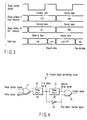
CPU 11 and thememory 12 through thedata bus 14, thepseudo-data generating circuit 19 generates pseudo-data and outputs the pseudo-data onto thedata bus 14. - FIG. 3 shows a timing chart showing the operation of the data processing apparatus shown in FIG. 1 in the case where general data and secret data are successively read out from the
memory 12. - A read pattern A is that general data of 00h is read out before reading out secret data of 00h, for example (h denotes hexadecimal data). A read pattern B is that secret data of FFh is read out after reading out general data of 00h.
- In the case of the read pattern A, the general data and the secret data are the same as each other, and therefore, power consumption by the bus driving circuit provided in the
memory 12 changes little at the time of the reading of the secret data. On the other hand, in the case of the read pattern B, all bit data of the general data are different from those of the secret data, and therefore, power consumption by the bus driving circuit provided in thememory 12 changes greatly at the time of the reading of the secret data. In this case, a current change of the power supply voltage is externally observed to examine the correlation between the current change of the power supply voltage at the time of transmission of the general data and the current change of the power supply voltage at the time of transmission of the secret data, and thus the secret data transmitted on thedata bus 14 is likely to undergo analysis. Secret data other than the secret data of FFh is read out in the same manner. - In the first embodiment, as shown in FIG. 3, pseudo-data is outputted onto the
data bus 14 between the reading of the general data and the reading of the secret data (incidentally, the pseudo-data is indicated by xxh, and xx represents any logical level). Since the pseudo-data is randomly generated, the secret data cannot be known from the correlation even if the correlation between the current change of the power supply voltage at the time of transmission of the pseudo-data and the current change of the power supply voltage at the time of transmission of the secret data is examined. Accordingly, the data processing apparatus of the first embodiment can prevent leakage of secret data. - A data processing apparatus provided with a random number data generating circuit is disclosed in Jpn. Pat. Appln. KOKAI Publication No. 8-249239. Random number data generated by the random number data generating circuit is transferred on a data bus and then fetched by a CPU, and the CPU performs operation processing using the random number data. In the data processing apparatus described in the publication, the random number data is, however, handled as part of normal data and thus transferred to the CPU through the data bus within the read cycle period. In other words, the data processing apparatus described in the publication is different from the data processing apparatus of the above-described embodiment in which pseudo-data is generated and outputted onto the data bus after the read cycle period or the write cycle period. When the random number data is transferred through the data bus within the read cycle period, the random number data is regarded as original data. Consequently, the random number data is correlated with data prior to and subsequent to the random number data, so that the data is analyzed in accordance with the correlation.
- In the above-described embodiment, the description is given with regard to the case where the
pseudo-data generating circuit 19 generates pseudo-data and outputs the pseudo-data onto thedata bus 14 after the read cycle period and the write cycle period when original data is transferred between theCPU 11 and thememory 12 through thedata bus 14, or after the read cycle period and the read cycle period. However, thepseudo-data generating circuit 19 may generate pseudo-data and output the pseudo-data onto thedata bus 14 between two operation cycle periods forming any of combinations of the read cycle period and the write cycle period when original data is transferred between theCPU 11 and thememory 12 through thedata bus 14, namely, between the read cycle period and the write cycle period, between the write cycle period and the read cycle period, between two read cycle periods, or between two write cycle periods. - For example, the description of the operation with reference to FIG. 2 is given using as an example the case where data from the
CPU 11 is written in thememory 12 after data stored in thememory 12 is read out by theCPU 11 accessing thememory 12. However, this can be easily inferred also in the case where a plurality of read operations take place in succession as shown in FIG. 3 or the case where a plurality of write operations take place in succession, and therefore the description of these operations is omitted. - FIG. 4 shows an example of a specific circuit configuration of the control
signal generating circuit 18 shown in FIG. 1. This circuit includes: an ORcircuit 31 to which the read control signal and the write control signal are inputted; adelay circuit 32 which causes theOR circuit 31 to delay outputting the signal for a predetermined period and outputs a first delay signal; adelay circuit 33 which causes the first delay signal to further delay for a predetermined period and outputs a second delay signal; aninverter circuit 34 which inverts the first delay signal and outputs a first delay inverted signal; and anOR circuit 35 to which the second delay signal and the first delay inverted signal are inputted. - FIG. 5 is a timing chart showing a signal waveform of a principal part of the control
signal generating circuit 18 shown in FIG. 4. In FIG. 5, td1 and td2 denote the signal delay times of thedelay circuits - In the read cycle period or the write cycle period, the read control signal or the write control signal drops to "0" level, then the control signal returns to the "1"-level initial value, and thereafter the control signal becomes active after a lapse of the delay time td1 of the
delay circuit 32. After that, the control signal becomes inactive after a lapse of the delay time td2 of thedelay circuit 33. - Of course, the circuit configuration of the control
signal generating circuit 18 is not limited to the circuit configuration shown in FIG. 4. In short, any circuit configuration may be adopted as long as it can detect a change in the read control signal and the write control signal and generate a control signal. - FIG. 6 is a block diagram showing the whole configuration of a data processing apparatus according to a second embodiment of the invention.
- The data processing apparatus of the second embodiment is different from the data processing apparatus of the above-described first embodiment shown in FIG. 1 in that the
pseudo-data generating circuit 19 is replaced by adummy circuit 23. Therefore, the parts corresponding to the parts shown in FIG. 1 are indicated by the same reference numerals, the description of the corresponding parts is omitted, and the description is given below with regard to only the points of difference between the data processing apparatuses shown in FIGS. 1 and 6. - The
dummy circuit 23 is controlled so as to operate in accordance with a control signal generated by the controlsignal generating circuit 18. When operating, thedummy circuit 23 consumes power to count clock signals. Thedummy circuit 23 may include a counter circuit, a shift register or the like, for example. - According to the second embodiment, the
dummy circuit 23 operates and consumes power between two operation cycle periods forming any of combinations of the read cycle period and the write cycle period when original data is transmitted/received between theCPU 11 and thememory 12 through thedata bus 14, and therefore, power consumption for transfer of two sets of original data including secret data to be transferred between theCPU 11 and thememory 12 is different from power consumption for operation of thedummy circuit 23 during the transfer. - Therefore, the secret data cannot be known from the correlation even if the correlation between a current change of the power supply voltage at the time of operation of the
dummy circuit 23 and a current change of the power supply voltage at the time of transmission of the secret data is examined. Accordingly, the data processing apparatus of the second embodiment can also prevent leakage of secret data. - FIG. 7 is a block diagram showing the whole configuration of a memory card to which the data processing apparatus shown in FIG. 1 is applied. The parts corresponding to the parts shown in FIG. 1 are indicated by the same reference numerals, and the description of the corresponding parts is omitted.
- A
memory card 30 is internally provided with aperipheral logic circuit 31 and ananalog circuit 32, in addition to theCPU 11, thememory 12, thebus folder 17, the controlsignal generating circuit 18 and thepseudo-data generating circuit 19. In FIG. 7, the address bus 13, theread signal line 15 and thewrite signal line 16 are shown as one address/read-write signal bus 33 having a predetermined number of bits. - The
peripheral logic circuit 31 receives a reset signal RESET and a clock signal CLK inputted from an apparatus provided external to thememory card 30, supplies the signals to each circuit in thememory card 30, and performs data transfer between the external apparatus and theinternal data bus 14 through an external I/O. - The above-mentioned
memory 12 includes, for example, aROM 12A, aRAM 12B and anEEPROM 12C as shown in FIG. 7. - The
analog circuit 32 generates various types of voltages required for theEEPROM 12C in thememory 12 to operate by an external power supply voltage Vcc, and supplies the voltages to theEEPROM 12C. The above-mentioned secret data is previously stored in theEEPROM 12C, for example. - In the memory card having the above-described configuration, general data is read out from the
ROM 12A, theRAM 12B or theEEPROM 12C, and thereafter, when the secret data previously stored in theEEPROM 12C is read out, pseudo-data is outputted onto thedata bus 14 between the read cycle period of the general data and the read cycle period of the secret data. Therefore, the memory card can achieve the effect of preventing leakage of secret data as in the case of the above-described first embodiment. - FIG. 8 is a block diagram showing the whole configuration of a memory card to which the data processing apparatus shown in FIG. 6 is applied. The parts corresponding to the parts shown in FIG. 6 are indicated by the same reference numerals, and the description of the corresponding parts is omitted.
- The
memory card 30 is internally provided with theperipheral logic circuit 31 and theanalog circuit 32, in addition to theCPU 11, thememory 12, thebus folder 17, the controlsignal generating circuit 18 and thedummy circuit 23. Also in this case, in FIG. 8, the address bus 13, theread signal line 15 and thewrite signal line 16 are shown as one address/read-write signal bus 33 having a predetermined number of bits. - In the same manner as the
peripheral logic circuit 31 shown in FIG. 7, theperipheral logic circuit 31 receives the reset signal RESET and the clock signal CLK inputted from the apparatus provided external to thememory card 30, supplies the signals to each circuit in thememory card 30, and performs data transmitted/received between the external apparatus and theinternal data bus 14 through the external I/O. - The above-mentioned
memory 12 includes, for example, theROM 12A, theRAM 12B and theEEPROM 12C in the same manner as thememory 12 shown in FIG. 7. - The
analog circuit 32 generates various types of voltages required for theEEPROM 12C to operate by the external power supply voltage Vcc in the same manner as theanalog circuit 32 shown in FIG. 7. - In the memory card having the above-described configuration, general data is read out from the
ROM 12A, theRAM 12B or theEEPROM 12C, and thereafter, when the secret data previously stored in theEEPROM 12C is read out, thedummy circuit 23 operates and consumes power between the read cycle period of the general data and the read cycle period of the secret data. Therefore, the memory card can achieve the effect of preventing leakage of secret data as in the case of the above-described second embodiment.
Claims (14)
- A data processing apparatus characterized by comprising:an operation processing unit (11) having at least a read cycle period when said operation processing unit (11) reads data from a device, and a write cycle period when said operation processing unit (11) writes data in the device;a memory (12) which performs data transfer between said operation processing unit (11) and said memory (12);a data bus (14) connected to said operation processing unit (11) and said memory (12); anda pseudo-data generating circuit (19) connected to said data bus (14), said circuit (19) generates pseudo-data and outputs the pseudo-data to said data bus (14) in a time interval between the read cycle period and the write cycle period, between the write cycle period and the read cycle period, between two read cycle periods, or between two write cycle periods.
- The data processing apparatus according to claim 1, characterized in that said data processing apparatus further comprising a read signal line (15) and a write signal line (16) connected to said operation processing unit (11) and said memory (12), and a control signal generating circuit (18) connected to said read signal line (15) and said write signal line (16), said circuit (18) detects a change in a read control signal and a write control signal transmitted to said read signal line (15) and said write signal line (16), respectively, and then generates a control signal, and
said pseudo-data generating circuit (19) receives the control signal generated by said control signal generating circuit (18) and generates the pseudo-data in accordance with the control signal. - The data processing apparatus according to claim 1, characterized in that said pseudo-data generating circuit (19) generates random number data as the pseudo-data.
- A data processing apparatus characterized by comprising:an operation processing unit (11) having at least a read cycle period when said operation processing unit (11) reads data from a device, and a write cycle period when said operation processing unit (11) writes data in the device;a memory (12) which performs data transfer between said operation processing unit (11) and said memory (12);a data bus (14) connected to said operation processing unit (11) and said memory (12); anda dummy circuit (23) connected to said data bus (14), said circuit (23) operates and consumes power in a time interval between the read cycle period and the write cycle period, between the write cycle period and the read cycle period, between two read cycle periods, or between two write cycle periods.
- The data processing apparatus according to claim 4, characterized in that said data processing apparatus further comprising a read signal line (15) and a write signal line (16) connected to said operation processing unit (11) and said memory (12), and a control signal generating circuit (18) connected to said read signal line (15) and said write signal line (16), said circuit (18) detects a change in a read control signal and a write control signal transmitted to said read signal line (15) and said write signal line (16), respectively, and then generates a control signal, and
said dummy circuit (23) receives the control signal generated by said control signal generating circuit (18) and is controlled so as to operate in accordance with the control signal. - The data processing apparatus according to claim 4, characterized in that said dummy circuit (23) is a counter circuit.
- The data processing apparatus according to claim 4, characterized in that said dummy circuit (23) is a shift register circuit.
- A memory card characterized by comprising:an operation processing unit (11) having at least a read cycle period when said operation processing unit (11) reads data from a device, and a write cycle period when said operation processing unit (11) writes data in the device;a memory (12) which performs data transfer between said operation processing unit (11) and said memory (12);a data bus (14) connected to said operation processing unit (11) and said memory (12);an input/output circuit (31) connected to said data bus (14), said circuit (31) outputs external data onto said data bus (14) and outputs data on said data bus (14) to an external apparatus; anda pseudo-data generating circuit (19) connected to said data bus (14), said circuit (19) generates pseudo-data and outputs the pseudo-data to said data bus (14) in a time interval between the read cycle period and the write cycle period, between the write cycle period and the read cycle period, between two read cycle periods, or between two write cycle periods.
- The memory card according to claim 8, characterized in that said memory card further comprising a read signal line (15) and a write signal line (16) connected to said operation processing unit (11) and said memory (12), and a control signal generating circuit (18) connected to said read signal line (15) and said write signal line (16), said circuit (18) detects a change in a read control signal and a write control signal transmitted to said read signal line (15) and said write signal line (16), respectively, and then generates a control signal, and
said pseudo-data generating circuit (19) receives the control signal generated by said control signal generating circuit (18) and generates the pseudo-data in accordance with the control signal. - The memory card according to claim 8, characterized in that said pseudo-data generating circuit (19) generates random number data as the pseudo-data.
- A memory card characterized by comprising:an operation processing unit (11) having at least a read cycle period when said operation processing unit (11) reads data from a device, and a write cycle period when said operation processing unit (11) writes data in the device;a memory (12) which performs data transfer between said operation processing unit (11) and said memory (12);a data bus (14) connected to said operation processing unit (11) and said memory (12);an input/output circuit (31) connected to said data bus (14), said circuit (31) outputs external data onto said data bus (14) and outputs data on said data bus (14) to an external apparatus; anda dummy circuit (23) connected to said data bus (14), said circuit (23) operates and consumes power in a time interval between the read cycle period and the write cycle period, between the write cycle period and the read cycle period, between two read cycle periods, or between two write cycle periods.
- The memory card according to claim 11, characterized in that said memory card further comprising a read signal line (15) and a write signal line (16) connected to said operation processing unit (11) and said memory (12), and a control signal generating circuit (18) connected to said read signal line (15) and said write signal line (16), said circuit (18) detects a change in a read control signal and a write control signal transmitted to said read signal line (15) and said write signal line (16), respectively, and then generates a control signal, and
said dummy circuit (23) receives the control signal generated by said control signal generating circuit (18) and is controlled so as to operate in accordance with the control signal. - The memory card according to claim 11, characterized in that said dummy circuit (23) is a counter circuit.
- The memory card according to claim 11, characterized in that said dummy circuit (23) is a shift register circuit.
Applications Claiming Priority (2)
| Application Number | Priority Date | Filing Date | Title |
|---|---|---|---|
| JP2000400828A JP3977592B2 (en) | 2000-12-28 | 2000-12-28 | Data processing device |
| JP2000400828 | 2000-12-28 |
Publications (3)
| Publication Number | Publication Date |
|---|---|
| EP1220077A2 true EP1220077A2 (en) | 2002-07-03 |
| EP1220077A3 EP1220077A3 (en) | 2003-07-02 |
| EP1220077B1 EP1220077B1 (en) | 2007-05-09 |
Family
ID=18865346
Family Applications (1)
| Application Number | Title | Priority Date | Filing Date |
|---|---|---|---|
| EP01130510A Expired - Lifetime EP1220077B1 (en) | 2000-12-28 | 2001-12-21 | Data processing apparatus and memory card using the same |
Country Status (7)
| Country | Link |
|---|---|
| US (1) | US7533275B2 (en) |
| EP (1) | EP1220077B1 (en) |
| JP (1) | JP3977592B2 (en) |
| KR (1) | KR100486808B1 (en) |
| CN (1) | CN1230734C (en) |
| DE (1) | DE60128323T2 (en) |
| TW (1) | TW573274B (en) |
Cited By (1)
| Publication number | Priority date | Publication date | Assignee | Title |
|---|---|---|---|---|
| EP1553500A1 (en) * | 2004-01-07 | 2005-07-13 | Deutsche Thomson-Brandt Gmbh | Method and apparatus for indication of valid data |
Families Citing this family (11)
| Publication number | Priority date | Publication date | Assignee | Title |
|---|---|---|---|---|
| US7949883B2 (en) * | 2004-06-08 | 2011-05-24 | Hrl Laboratories, Llc | Cryptographic CPU architecture with random instruction masking to thwart differential power analysis |
| JP4594665B2 (en) * | 2004-07-09 | 2010-12-08 | 三菱電機株式会社 | Tamper resistant circuit evaluation apparatus, tamper resistant circuit evaluation method, signal generation circuit, signal generation method, tamper resistance evaluation apparatus, and tamper resistance evaluation method |
| TWI263431B (en) * | 2004-09-22 | 2006-10-01 | Inst Information Industry | Data encryption system and method |
| KR101311963B1 (en) | 2007-08-06 | 2013-09-26 | 삼성전자주식회사 | Semiconductor memory device capable of writing and reading safely from power attack and method thereof |
| JP5359603B2 (en) * | 2009-06-25 | 2013-12-04 | セイコーエプソン株式会社 | Integrated circuit system, data writing method, and data reading method |
| JP5926655B2 (en) * | 2012-08-30 | 2016-05-25 | ルネサスエレクトロニクス株式会社 | Central processing unit and arithmetic unit |
| JP7177506B2 (en) * | 2020-03-09 | 2022-11-24 | 京楽産業.株式会社 | game machine |
| JP7177503B2 (en) * | 2020-03-09 | 2022-11-24 | 京楽産業.株式会社 | game machine |
| JP7177507B2 (en) * | 2020-03-09 | 2022-11-24 | 京楽産業.株式会社 | game machine |
| JP7177505B2 (en) * | 2020-03-09 | 2022-11-24 | 京楽産業.株式会社 | game machine |
| JP7177504B2 (en) * | 2020-03-09 | 2022-11-24 | 京楽産業.株式会社 | game machine |
Citations (6)
| Publication number | Priority date | Publication date | Assignee | Title |
|---|---|---|---|---|
| GB2119978A (en) * | 1982-05-06 | 1983-11-23 | Philips Nv | Device for protection against the unauthorized reading of program words stored in a memory |
| US4932053A (en) * | 1988-11-10 | 1990-06-05 | Sgs-Thomson Microelectronics, S.A. | Safety device against the unauthorized detection of protected data |
| FR2776410A1 (en) * | 1998-03-20 | 1999-09-24 | Gemplus Card Int | Device to protect microprocessor card against fraudulent analysis of operations performed by measuring current consumed |
| WO2000026746A2 (en) * | 1998-11-03 | 2000-05-11 | Koninklijke Philips Electronics N.V. | Data carrier with obscured power consumption |
| FR2787900A1 (en) * | 1998-12-28 | 2000-06-30 | Bull Cp8 | INTELLIGENT INTEGRATED CIRCUIT |
| FR2793904A1 (en) * | 1999-05-21 | 2000-11-24 | St Microelectronics Sa | Control of the current taken by an electronic circuit used in reading the security code from a device such as a bankers card of portable telephone to mask the period during which the code is read, but to reduce the masking period |
Family Cites Families (10)
| Publication number | Priority date | Publication date | Assignee | Title |
|---|---|---|---|---|
| JPH02242327A (en) * | 1989-03-15 | 1990-09-26 | Oki Electric Ind Co Ltd | Random number generator |
| FR2728369B1 (en) | 1994-12-19 | 1997-01-31 | Sgs Thomson Microelectronics | METHOD AND DEVICE FOR INCREASING THE SECURITY OF AN INTEGRATED CIRCUIT |
| JPH0926917A (en) | 1995-07-11 | 1997-01-28 | Ekushingu:Kk | Memory device |
| DE19642560A1 (en) | 1996-10-15 | 1998-04-16 | Siemens Ag | Electronic data processing circuit |
| DE69938045T2 (en) * | 1998-06-03 | 2009-01-15 | Cryptography Research Inc., San Francisco | Use of unpredictable information to minimize the leak of chip cards and other cryptosystems |
| JP2000165375A (en) * | 1998-11-30 | 2000-06-16 | Hitachi Ltd | Information processor and ic card |
| JP2000285094A (en) | 1999-03-31 | 2000-10-13 | Kawasaki Steel Corp | Microcomputer having built-in eeprom |
| US6419159B1 (en) * | 1999-06-14 | 2002-07-16 | Microsoft Corporation | Integrated circuit device with power analysis protection circuitry |
| FR2796738B1 (en) * | 1999-07-22 | 2001-09-14 | Schlumberger Systems & Service | SECURE MICRO-CONTROLLER AGAINST CURRENT ATTACKS |
| FR2808360B1 (en) * | 2000-04-28 | 2002-06-28 | Gemplus Card Int | COUNTER MEASUREMENT METHOD IN A MICROCIRCUIT IMPLEMENTING THE METHOD AND CHIP CARD COMPRISING SAID MICROCIRCUIT |
-
2000
- 2000-12-28 JP JP2000400828A patent/JP3977592B2/en not_active Expired - Fee Related
-
2001
- 2001-12-21 EP EP01130510A patent/EP1220077B1/en not_active Expired - Lifetime
- 2001-12-21 TW TW90131799A patent/TW573274B/en not_active IP Right Cessation
- 2001-12-21 DE DE60128323T patent/DE60128323T2/en not_active Expired - Lifetime
- 2001-12-27 KR KR10-2001-0085955A patent/KR100486808B1/en not_active IP Right Cessation
- 2001-12-27 US US10/026,813 patent/US7533275B2/en not_active Expired - Fee Related
- 2001-12-28 CN CNB011440899A patent/CN1230734C/en not_active Expired - Fee Related
Patent Citations (6)
| Publication number | Priority date | Publication date | Assignee | Title |
|---|---|---|---|---|
| GB2119978A (en) * | 1982-05-06 | 1983-11-23 | Philips Nv | Device for protection against the unauthorized reading of program words stored in a memory |
| US4932053A (en) * | 1988-11-10 | 1990-06-05 | Sgs-Thomson Microelectronics, S.A. | Safety device against the unauthorized detection of protected data |
| FR2776410A1 (en) * | 1998-03-20 | 1999-09-24 | Gemplus Card Int | Device to protect microprocessor card against fraudulent analysis of operations performed by measuring current consumed |
| WO2000026746A2 (en) * | 1998-11-03 | 2000-05-11 | Koninklijke Philips Electronics N.V. | Data carrier with obscured power consumption |
| FR2787900A1 (en) * | 1998-12-28 | 2000-06-30 | Bull Cp8 | INTELLIGENT INTEGRATED CIRCUIT |
| FR2793904A1 (en) * | 1999-05-21 | 2000-11-24 | St Microelectronics Sa | Control of the current taken by an electronic circuit used in reading the security code from a device such as a bankers card of portable telephone to mask the period during which the code is read, but to reduce the masking period |
Non-Patent Citations (1)
| Title |
|---|
| "SECTION 1: INTRODUCTION" DATA BOOK SOFT MICROCONTROLLER, XX, XX, 6 October 1993 (1993-10-06), pages 1-3,7-8,73-229,290-292, XP002053731 * |
Cited By (1)
| Publication number | Priority date | Publication date | Assignee | Title |
|---|---|---|---|---|
| EP1553500A1 (en) * | 2004-01-07 | 2005-07-13 | Deutsche Thomson-Brandt Gmbh | Method and apparatus for indication of valid data |
Also Published As
| Publication number | Publication date |
|---|---|
| DE60128323T2 (en) | 2008-01-10 |
| US20020084333A1 (en) | 2002-07-04 |
| DE60128323D1 (en) | 2007-06-21 |
| JP2002202916A (en) | 2002-07-19 |
| EP1220077B1 (en) | 2007-05-09 |
| CN1230734C (en) | 2005-12-07 |
| JP3977592B2 (en) | 2007-09-19 |
| US7533275B2 (en) | 2009-05-12 |
| TW573274B (en) | 2004-01-21 |
| EP1220077A3 (en) | 2003-07-02 |
| KR100486808B1 (en) | 2005-05-03 |
| CN1362662A (en) | 2002-08-07 |
| KR20020055422A (en) | 2002-07-08 |
Similar Documents
| Publication | Publication Date | Title |
|---|---|---|
| KR100365386B1 (en) | Semiconductor memory system, its operation method and maximum delay time measurement method | |
| EP0464433A2 (en) | Microcontroller device having remotely programmable EPROM & method of programming | |
| US6421291B1 (en) | Semiconductor memory device having high data input/output frequency and capable of efficiently testing circuit associated with data input/output | |
| US20080189555A1 (en) | Smart cards including separate clocks for key processing and non-volatile memory interface communications and methods of operating the same | |
| EP1220077A2 (en) | Data processing apparatus and memory card using the same | |
| US20070038795A1 (en) | Asynchronous bus interface and processing method thereof | |
| CN110892483B (en) | Method for testing memory device using limited number of test pins and memory device using the same | |
| US5884074A (en) | Microcomputer utilizing flash memory for data storage | |
| US6158036A (en) | Merged memory and logic (MML) integrated circuits including built-in test circuits and methods | |
| US6543019B2 (en) | Method for built-in self test of an electronic circuit | |
| US6892269B2 (en) | Nonvolatile memory device with double serial/parallel communication interface | |
| US5734841A (en) | Circuit for plug/play in peripheral component interconnect bus | |
| US7782682B2 (en) | Semiconductor device with circuitry for efficient information exchange | |
| WO2008024336A2 (en) | Write data mask method and system | |
| KR100327637B1 (en) | Burst Mode Semiconductor Memory Device | |
| US6611929B1 (en) | Test circuit for memory | |
| US6876564B2 (en) | Integrated circuit device and method for applying different types of signals to internal circuit via one pin | |
| US6226211B1 (en) | Merged memory-logic semiconductor device having a built-in self test circuit | |
| JP2001243797A (en) | Semiconductor device and test method | |
| US5818794A (en) | Internally controlled signal system for controlling the operation of a device | |
| US6088271A (en) | Method and apparatus for transferring signal to circuit without waveform distortion | |
| JP2877505B2 (en) | LSI mounting board and data processing device | |
| US6038617A (en) | Auto configuration of a serial ROM by sensing an output of the serial ROM after transmission of a read instruction and an x-bit address to it's input | |
| US20080147919A1 (en) | Semiconductor memory device | |
| US5943492A (en) | Apparatus and method for generating external interface signals in a microprocessor |
Legal Events
| Date | Code | Title | Description |
|---|---|---|---|
| PUAI | Public reference made under article 153(3) epc to a published international application that has entered the european phase |
Free format text: ORIGINAL CODE: 0009012 |
|
| 17P | Request for examination filed |
Effective date: 20011221 |
|
| AK | Designated contracting states |
Kind code of ref document: A2 Designated state(s): AT BE CH CY DE DK ES FI FR GB GR IE IT LI LU MC NL PT SE TR |
|
| AX | Request for extension of the european patent |
Free format text: AL;LT;LV;MK;RO;SI |
|
| RIC1 | Information provided on ipc code assigned before grant |
Ipc: 7G 07F 7/10 B Ipc: 7G 06F 1/00 A |
|
| PUAL | Search report despatched |
Free format text: ORIGINAL CODE: 0009013 |
|
| AK | Designated contracting states |
Designated state(s): AT BE CH CY DE DK ES FI FR GB GR IE IT LI LU MC NL PT SE TR |
|
| AX | Request for extension of the european patent |
Extension state: AL LT LV MK RO SI |
|
| AKX | Designation fees paid |
Designated state(s): DE FR GB |
|
| 17Q | First examination report despatched |
Effective date: 20040304 |
|
| GRAP | Despatch of communication of intention to grant a patent |
Free format text: ORIGINAL CODE: EPIDOSNIGR1 |
|
| RIC1 | Information provided on ipc code assigned before grant |
Ipc: G06F 21/00 20060101AFI20060616BHEP Ipc: G07F 7/10 20060101ALI20060616BHEP |
|
| GRAS | Grant fee paid |
Free format text: ORIGINAL CODE: EPIDOSNIGR3 |
|
| GRAA | (expected) grant |
Free format text: ORIGINAL CODE: 0009210 |
|
| AK | Designated contracting states |
Kind code of ref document: B1 Designated state(s): DE FR GB |
|
| REG | Reference to a national code |
Ref country code: GB Ref legal event code: FG4D |
|
| REF | Corresponds to: |
Ref document number: 60128323 Country of ref document: DE Date of ref document: 20070621 Kind code of ref document: P |
|
| ET | Fr: translation filed | ||
| PLBE | No opposition filed within time limit |
Free format text: ORIGINAL CODE: 0009261 |
|
| STAA | Information on the status of an ep patent application or granted ep patent |
Free format text: STATUS: NO OPPOSITION FILED WITHIN TIME LIMIT |
|
| 26N | No opposition filed |
Effective date: 20080212 |
|
| REG | Reference to a national code |
Ref country code: FR Ref legal event code: PLFP Year of fee payment: 15 |
|
| PGFP | Annual fee paid to national office [announced via postgrant information from national office to epo] |
Ref country code: GB Payment date: 20151216 Year of fee payment: 15 Ref country code: DE Payment date: 20151215 Year of fee payment: 15 |
|
| PGFP | Annual fee paid to national office [announced via postgrant information from national office to epo] |
Ref country code: FR Payment date: 20151110 Year of fee payment: 15 |
|
| REG | Reference to a national code |
Ref country code: DE Ref legal event code: R119 Ref document number: 60128323 Country of ref document: DE |
|
| GBPC | Gb: european patent ceased through non-payment of renewal fee |
Effective date: 20161221 |
|
| REG | Reference to a national code |
Ref country code: FR Ref legal event code: ST Effective date: 20170831 |
|
| PG25 | Lapsed in a contracting state [announced via postgrant information from national office to epo] |
Ref country code: FR Free format text: LAPSE BECAUSE OF NON-PAYMENT OF DUE FEES Effective date: 20170102 |
|
| PG25 | Lapsed in a contracting state [announced via postgrant information from national office to epo] |
Ref country code: DE Free format text: LAPSE BECAUSE OF NON-PAYMENT OF DUE FEES Effective date: 20170701 Ref country code: GB Free format text: LAPSE BECAUSE OF NON-PAYMENT OF DUE FEES Effective date: 20161221 |