EP1218806B1 - Method and apparatus for monitoring controller performance using statistical process control - Google Patents
Method and apparatus for monitoring controller performance using statistical process control Download PDFInfo
- Publication number
- EP1218806B1 EP1218806B1 EP00928556A EP00928556A EP1218806B1 EP 1218806 B1 EP1218806 B1 EP 1218806B1 EP 00928556 A EP00928556 A EP 00928556A EP 00928556 A EP00928556 A EP 00928556A EP 1218806 B1 EP1218806 B1 EP 1218806B1
- Authority
- EP
- European Patent Office
- Prior art keywords
- controller
- manufacturing
- processing
- analysis
- control
- Prior art date
- Legal status (The legal status is an assumption and is not a legal conclusion. Google has not performed a legal analysis and makes no representation as to the accuracy of the status listed.)
- Expired - Lifetime
Links
- 238000000034 method Methods 0.000 title claims description 105
- 238000003070 Statistical process control Methods 0.000 title claims description 32
- 238000012544 monitoring process Methods 0.000 title claims description 18
- 238000004519 manufacturing process Methods 0.000 claims description 144
- 239000004065 semiconductor Substances 0.000 claims description 74
- 230000008569 process Effects 0.000 claims description 68
- 238000012545 processing Methods 0.000 claims description 61
- 238000004458 analytical method Methods 0.000 claims description 48
- 238000012986 modification Methods 0.000 claims description 18
- 230000004048 modification Effects 0.000 claims description 18
- 238000004364 calculation method Methods 0.000 claims description 12
- 238000001514 detection method Methods 0.000 claims description 11
- 238000004886 process control Methods 0.000 claims description 9
- 230000004044 response Effects 0.000 claims description 2
- 235000012431 wafers Nutrition 0.000 description 44
- 238000013515 script Methods 0.000 description 6
- 238000004590 computer program Methods 0.000 description 4
- 238000011161 development Methods 0.000 description 4
- 230000018109 developmental process Effects 0.000 description 4
- 238000000206 photolithography Methods 0.000 description 4
- 238000012552 review Methods 0.000 description 4
- 230000032683 aging Effects 0.000 description 3
- 230000008901 benefit Effects 0.000 description 3
- 230000008859 change Effects 0.000 description 3
- 238000011217 control strategy Methods 0.000 description 3
- 238000012360 testing method Methods 0.000 description 3
- 238000002872 Statistical quality control Methods 0.000 description 2
- 230000009471 action Effects 0.000 description 2
- 230000015556 catabolic process Effects 0.000 description 2
- 230000001276 controlling effect Effects 0.000 description 2
- 230000007547 defect Effects 0.000 description 2
- 238000006731 degradation reaction Methods 0.000 description 2
- 238000013461 design Methods 0.000 description 2
- 230000000694 effects Effects 0.000 description 2
- 238000005516 engineering process Methods 0.000 description 2
- 239000000463 material Substances 0.000 description 2
- 238000005498 polishing Methods 0.000 description 2
- 238000003908 quality control method Methods 0.000 description 2
- 238000013519 translation Methods 0.000 description 2
- 238000006243 chemical reaction Methods 0.000 description 1
- 238000004891 communication Methods 0.000 description 1
- 238000010276 construction Methods 0.000 description 1
- 230000002596 correlated effect Effects 0.000 description 1
- 230000000875 corresponding effect Effects 0.000 description 1
- 239000013078 crystal Substances 0.000 description 1
- 238000013500 data storage Methods 0.000 description 1
- 238000010586 diagram Methods 0.000 description 1
- 238000005530 etching Methods 0.000 description 1
- 238000004880 explosion Methods 0.000 description 1
- 238000013100 final test Methods 0.000 description 1
- 238000005259 measurement Methods 0.000 description 1
- 238000004806 packaging method and process Methods 0.000 description 1
- 238000007517 polishing process Methods 0.000 description 1
- 238000007619 statistical method Methods 0.000 description 1
Images


Classifications
-
- H—ELECTRICITY
- H01—ELECTRIC ELEMENTS
- H01L—SEMICONDUCTOR DEVICES NOT COVERED BY CLASS H10
- H01L22/00—Testing or measuring during manufacture or treatment; Reliability measurements, i.e. testing of parts without further processing to modify the parts as such; Structural arrangements therefor
-
- G—PHYSICS
- G05—CONTROLLING; REGULATING
- G05B—CONTROL OR REGULATING SYSTEMS IN GENERAL; FUNCTIONAL ELEMENTS OF SUCH SYSTEMS; MONITORING OR TESTING ARRANGEMENTS FOR SUCH SYSTEMS OR ELEMENTS
- G05B19/00—Programme-control systems
- G05B19/02—Programme-control systems electric
- G05B19/418—Total factory control, i.e. centrally controlling a plurality of machines, e.g. direct or distributed numerical control [DNC], flexible manufacturing systems [FMS], integrated manufacturing systems [IMS] or computer integrated manufacturing [CIM]
- G05B19/41885—Total factory control, i.e. centrally controlling a plurality of machines, e.g. direct or distributed numerical control [DNC], flexible manufacturing systems [FMS], integrated manufacturing systems [IMS] or computer integrated manufacturing [CIM] characterised by modeling, simulation of the manufacturing system
-
- G—PHYSICS
- G05—CONTROLLING; REGULATING
- G05B—CONTROL OR REGULATING SYSTEMS IN GENERAL; FUNCTIONAL ELEMENTS OF SUCH SYSTEMS; MONITORING OR TESTING ARRANGEMENTS FOR SUCH SYSTEMS OR ELEMENTS
- G05B19/00—Programme-control systems
- G05B19/02—Programme-control systems electric
- G05B19/418—Total factory control, i.e. centrally controlling a plurality of machines, e.g. direct or distributed numerical control [DNC], flexible manufacturing systems [FMS], integrated manufacturing systems [IMS] or computer integrated manufacturing [CIM]
- G05B19/41875—Total factory control, i.e. centrally controlling a plurality of machines, e.g. direct or distributed numerical control [DNC], flexible manufacturing systems [FMS], integrated manufacturing systems [IMS] or computer integrated manufacturing [CIM] characterised by quality surveillance of production
-
- G—PHYSICS
- G05—CONTROLLING; REGULATING
- G05B—CONTROL OR REGULATING SYSTEMS IN GENERAL; FUNCTIONAL ELEMENTS OF SUCH SYSTEMS; MONITORING OR TESTING ARRANGEMENTS FOR SUCH SYSTEMS OR ELEMENTS
- G05B2219/00—Program-control systems
- G05B2219/30—Nc systems
- G05B2219/32—Operator till task planning
- G05B2219/32017—Adapt real process as function of changing simulation model, changing for better results
-
- G—PHYSICS
- G05—CONTROLLING; REGULATING
- G05B—CONTROL OR REGULATING SYSTEMS IN GENERAL; FUNCTIONAL ELEMENTS OF SUCH SYSTEMS; MONITORING OR TESTING ARRANGEMENTS FOR SUCH SYSTEMS OR ELEMENTS
- G05B2219/00—Program-control systems
- G05B2219/30—Nc systems
- G05B2219/32—Operator till task planning
- G05B2219/32191—Real time statistical process monitoring
-
- G—PHYSICS
- G05—CONTROLLING; REGULATING
- G05B—CONTROL OR REGULATING SYSTEMS IN GENERAL; FUNCTIONAL ELEMENTS OF SUCH SYSTEMS; MONITORING OR TESTING ARRANGEMENTS FOR SUCH SYSTEMS OR ELEMENTS
- G05B2219/00—Program-control systems
- G05B2219/30—Nc systems
- G05B2219/32—Operator till task planning
- G05B2219/32201—Build statistical model of past normal proces, compare with actual process
-
- G—PHYSICS
- G05—CONTROLLING; REGULATING
- G05B—CONTROL OR REGULATING SYSTEMS IN GENERAL; FUNCTIONAL ELEMENTS OF SUCH SYSTEMS; MONITORING OR TESTING ARRANGEMENTS FOR SUCH SYSTEMS OR ELEMENTS
- G05B2219/00—Program-control systems
- G05B2219/30—Nc systems
- G05B2219/42—Servomotor, servo controller kind till VSS
- G05B2219/42001—Statistical process control spc
-
- Y—GENERAL TAGGING OF NEW TECHNOLOGICAL DEVELOPMENTS; GENERAL TAGGING OF CROSS-SECTIONAL TECHNOLOGIES SPANNING OVER SEVERAL SECTIONS OF THE IPC; TECHNICAL SUBJECTS COVERED BY FORMER USPC CROSS-REFERENCE ART COLLECTIONS [XRACs] AND DIGESTS
- Y02—TECHNOLOGIES OR APPLICATIONS FOR MITIGATION OR ADAPTATION AGAINST CLIMATE CHANGE
- Y02P—CLIMATE CHANGE MITIGATION TECHNOLOGIES IN THE PRODUCTION OR PROCESSING OF GOODS
- Y02P90/00—Enabling technologies with a potential contribution to greenhouse gas [GHG] emissions mitigation
- Y02P90/02—Total factory control, e.g. smart factories, flexible manufacturing systems [FMS] or integrated manufacturing systems [IMS]
Definitions
- This invention relates generally to semiconductor products manufacturing, and, more particularly, to a method and apparatus for monitoring controller performance using statistical process control.
- US-A-5 661 669 discloses a system for run-to-run control of semiconductor wafer processing.
- the system is a model-based system that generates process parameters based on desired quality characteristics supplied by the user.
- the system may use a feedback loop to modify the model and to control equipment settings on a real-time, run-by-run basis.
- the system may adjust the model if the measured quality characteristics of the process, determined by a sensor, vary from the expected quality characteristics by more than a predetermined statistical amount.
- US-A-5 546 312 discloses a system and method for controlling one or multiple metrics of non-uniformity using a model form independent multi-variable controller.
- the method utilises process models relating product quality parameters to process control variables.
- the method measures a plurality of product quality parameters on a plurality of products and exercises statistical quality control tests.
- the process models are tuned by estimating a changed state of the processing, and from that, estimating new values for the process control variables.
- US-A-5 452 218 discloses a system and method for determining quality levels for fabrication and assembly designs using process capabilities stored in a database.
- a worksheet is used to model the manufactured product using process capability data retrieved from the database.
- the system displays the defects and totals them according to a predetermined criteria to produce a measure of quality.
- US-A-5 408 405 discloses a multi-variable statistical process controller for discrete manufacturing.
- the method utilises process models relating product quality parameters to process control variables.
- the method measures a plurality of product quality parameters on a first and a second plurality of products and exercises statistical quality control tests on the plurality of product quality parameters of the first plurality of products. If the tests on the first plurality of products are unsuccessful, the method tunes the process models to create tuned process models using the plurality of product quality parameters from the second plurality of products, the tuning estimating a changed state of the processing.
- the manufacture of semiconductor devices requires a number of discrete process steps to create a packaged semiconductor device from raw semiconductor material.
- the various processes from the initial growth of the semiconductor material, the slicing of the semiconductor crystal into individual wafers, the fabrication stages (etching, doping, ion implanting, or the like), to the packaging and final testing of the completed device, are so different from one another and specialized that the processes may be performed in different manufacturing locations that contain different control schemes.
- Overlay is one of several important steps in the photolithography area of semiconductor manufacturing. Overlay control involves measuring the misalignment between two successive patterned layers on the surface of a semiconductor device. Generally, minimization of misalignment errors is important to ensure that the multiple layers of the semiconductor devices are connected and functional. As technology facilitates smaller critical dimensions for semiconductor devices, the need to reduce misalignment errors increases dramatically.
- photolithography engineers currently analyze the overlay errors a few times a month. The results from the analysis of the overlay errors are used to make updates to exposure tool settings manually.
- a manufacturing model is employed to control the manufacturing processes. Some of the problems associated with the current methods include the fact that the exposure tool settings are only updated a few times a month. Furthermore, currently the exposure tool updates are performed manually. Many times, errors in semiconductor manufacturing are not organized and reported to quality control personel. Often, the manufacturing models themselves incur bias errors that could compromise manufacturing quality.
- a set of processing steps is performed on a lot of wafers on a semiconductor manufacturing tool called an exposure tool or a stepper.
- the manufacturing tool communicates with a manufacturing framework or a network of processing modules.
- the manufacturing tool is generally connected to an equipment interface.
- the equipment interface is connected to a machine interface to which the stepper is connected, thereby facilitating communications between the stepper and the manufacturing framework.
- the machine interface can generally be part of an advanced process control (APC) system.
- the APC system initiates a control script based upon a manufacturing model, which can be a software program that automatically retrieves the data needed to execute a manufacturing process.
- semiconductor devices are staged through multiple manufacturing tools for multiple processes, generating data relating to the quality of the processed semiconductor devices.
- errors in semiconductor manufacturing are not organized and reported to quality control personel, which can result in reduced efficiency in manufacturing processes. Errors in the manufacturing model that is used to perform the manufacturing process, such as bias errors, often compromises the quality of manufactured products.
- the present invention is directed to overcoming, or at least reducing the effects of, one or more of the problems set forth above.
- a method for monitoring controller performance using statistical process control analysis.
- a manufacturing model is defined.
- a processing run of semiconductor devices is performed as defined by the manufacturing model and implemented by a process controller.
- a fault detection analysis is performed on the process controller.
- At least one control input signal generated by the process controller is updated.
- an apparatus for monitoring controller performance using statistical process control analysis.
- the apparatus of the present invention comprises: a processing tool coupled with the processing controller, a metrology tool interfaced with the processing tool; a control modification data calculation unit interfaced with the metrology and connected to the processing controller in a feedback manner; a predictor function interfaced with the processing controller; an statistical process control analysis unit interfaced with the predictor function and the processing tool; and a results versus prediction analysis unit interfaced with the statistical process control analysis unit and connected to the processing controller in a feedback manner.
- the present invention provides a method of acquiring production data and performing fault analysis on a process controller, such as a run-to-run controller, in response to the acquired production data.
- semiconductor products 105 such as semiconductor wafers are processed on processing tools 110, 112 using a plurality of control input signals on a line 120.
- the control input signals on the line 120 are sent to the processing tools 110, 112 from a computer system 130 via machine interfaces 115, 117.
- the first and second machine interfaces 115, 117 are located outside the processing tools 110, 112. In an alternative embodiment, the first and second machine interfaces 115, 117 are located within the processing tools 110, 112.
- the computer system 130 sends control input signals on a line 120 to the first and second machine interfaces 115, 117.
- the computer system 130 employs a manufacturing model 140 to generate the control input signals on the line 120.
- the manufacturing model 140 defines a process script and input control that implement a particular manufacturing process.
- the control input signals on a line 120 that are intended for processing tool A 110 are received and processed by the first machine interface 115.
- the control input signals on a line 120 that are intended for processing tool B 112 are received and processed by the second machine interface 117. Examples of the processing tools 110, 112 used in semiconductor manufacturing processes are steppers.
- the control inputs, on the line 120, that are used to operate the processing tools 110, 112 include an x-translation signal, a y-translation signal, an x-expansion wafer scale signal, a y-expansion wafer scale signal, a reticle magnification signal, and a reticle rotation signal.
- errors associated with the reticle magnification signal and the reticle rotation signal relate to one particular exposure process on the surface of the wafer being processed in the exposure tool.
- One of the primary features taught by the present invention is a method of detecting and organizing fault data for semiconductor manufacturing processes.
- the semiconductor product 105 or wafer that is being processed is examined in a review station.
- a review station is a KLA review station.
- One set of data derived from the operation of the review station is a quantitative measure of the amount of misregistration that was caused by the previous exposure process.
- the amount of misregistration relates to the misalignment in the process that occurred between two layers of a semiconductor wafer.
- the amount of misregistration that occurred can be attributed to the control inputs for a particular exposure process.
- the control inputs generally affect the accuracy of the process steps performed by the processing tools 110, 112 on the semiconductor wafer. Modifications of the control inputs can be utilized to improve the performance of the process steps employed in the manufacturing tool. Many times, the errors that are found in the processed semiconductor products 105 can be correlated to a particular fault analysis and corrective actions can be taken to reduce the errors.
- the manufacturing model 140 that is used by a process controller. such as an Advanced Process Control (APC) system, is defined, as described in block 210 of Figure 2.
- APC Advanced Process Control
- a manufacturing run of semiconductor devices such as semiconductor wafers
- a set of production data is collected, including measuring a plurality of wafer parameters, as described in block 230 of Figure 2.
- the wafer parameters include misalignment and misregistration errors during photolithography processes.
- the wafer parameters also include measuring post-polish thickness errors during a polishing process.
- the production data is used to update the manufacturing model 140, which is used by the process controller to modify control input signals for a subsequent manufacturing run of semiconductor wafers, as described in block 240 of Figure 2.
- the run-to-run controller then implements the next manufacturing run of semiconductor wafers and the feedback process is repeated as illustrated in Figure 2.
- an ideal manufacturing model 140 would result in random production errors that are distributed evenly over a Guassian-type error curve.
- non-random errors could occur.
- An error bias can develop within the manufacturing model resulting in consistent errors during semiconductor manufacturing.
- process steps there are over 300 process steps that are defined by a manufacturing model 140 and are implemented on a semiconductor wafer.
- a change in any one of the process steps can affect other related process steps such that the manufacturing model 140 that defines the process steps can become inaccurate.
- a chain reaction in the production of semiconductor wafers caused by a change in a particular process step can cause the manufacturing model 140 to no longer describe the process steps well, causing errors in production.
- a bias is created in the manufacturing model 140 such that now there is a consistent defect in the processed semiconductor wafers.
- a bias in the manufacturing model 140 can cause a 10 micro-meter misalignment error in every semiconductor wafer that is processed under the control of the manufacturing model 140.
- noise in the manufacturing system that is implementing the manufacturing model 140 that causes non-random errors that are outside a normal Guassian error curve.
- the aging of a manufacturing model 140 may cause degradation of output products that are manufactured within a manufacturing model 140 structure.
- a manufacturing model 140 can change its prior behavior.
- One example of aging of a manufacturing model 140 is degradation of lamps in an exposure tool.
- Implementation of the methods taught by the present invention can reduce the effects of aging of manufacturing models 140.
- the present invention teaches a method of implementing a statistical process control analysis method for reducing the bias and noise in manufacturing systems.
- SPC statistical process control
- SPC analysis is a method of monitoring, controlling, and, ideally, improving a process through statistical analysis.
- SPC analysis is comprised of four main steps. The main steps of SPC analysis include measuring the process, reducing variances in the process to make the process more consistent, monitoring the process, and improving the process to produce its best value.
- real-time SPC which can be used for run-to-run control applications in one embodiment, data is collected from the most recently finished manufacturing run of semiconductor wafers before the next manufacturing run of semiconductor wafers is processed. Steps are taken to ensure that the quality of the processed semiconductor wafers are as consistent as possible from one manufacturing run to another.
- SPC analysis rules dictate that causes of errors discovered during one manufacturing run of semiconductor wafers must be corrected before the next manufacturing run of semiconductor wafers is performed.
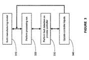
- a manufacturing model 140 that is used by a process controller such as an Advanced Process Control (APC) system, is defined, as described in block 310 of Figure 3.
- a manufacturing run of semiconductor devices such as semiconductor wafers
- a fault detection analysis is performed on the process controller, as described in block 330 of Figure 3.
- the fault detection analysis is performed on a process controller that is a run-to-run controller.
- FIG 4 after a manufacturing run of semiconductor wafers is completed, the corresponding production data is acquired, as described in block 410 of Figure 4.
- the production data that is acquired includes misalignment errors, misregistration errors, critical dimension errors, polishing thickness errors, and the like.
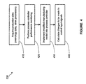
- a process controller performance monitoring step is performed, as described in block 420 of Figure 4. A more detailed depiction of the step of performing process controller performance monitoring described in block 420 of Figure 4, is illustrated in Figure 5.
- a manufacturing model 140 that is used by a process controller is defined, as described in block 510 of Figure 5.
- semiconductor wafers are processed using the manufacturing model, as described in block 520 of Figure 5.
- manufacturing parameters such as production data, are measured, as described in block 530 of Figure 5.
- the manufacturing parameters that are measured include misalignment errors, misregistration errors, critical dimension errors, and polishing thickness error.
- manufacturing parameters are measured using metrology tools.
- modification data is calculated for modifying parameters defined by the manufacturing model 140, as described in block 540 of Figure 5.
- SPC analysis which is described above, is performed after processing of semiconductor wafers, as described in block 550 of Figure 5.
- a prediction is made regarding the expected process behavior for a particular manufacturing model 140.
- the results from analysis of the semiconductor wafers is compared with the predicted process behavior, as described in block 560 of Figure 5.
- a judgment is made regarding how different the actual results from a processing step are from a set of predicted results for that processing step.
- standard SPC calculation methods that are known to those skilled in the art, and having the benefit of the present disclosure, are employed for SPC analysis for the present invention.
- the difference between the predicted process results and the actual process results is used to determine whether the manufacturing model 140 should be modified for the next manufacturing run of semiconductor wafers, thereby performing fault detection upon a run-to-run controller.
- the manufacturing model 140 is then modified to be used for subsequent manufacturing processes, as described in block 570 of Figure 5.
- the modification of the manufacturing model 140 described in block 570 completes the step of performing process control performance monitoring that is described in block 420 of Figure 4.
- the modified manufacturing model 140 is implemented into the process controller that controls subsequent processing of semiconductor devices, as described in block 430 of Figure 4.
- Modification factors needed to make modification to the control input signals on the line 120 are calculated, as described in block 440 of Figure 4.
- the completion of the calculations described in block 440 of Figure 4 completes the step of performing fault detection analysis on the process controller that is described in block 330 of Figure 3.
- the control input signal on the line 120 are modified to be used for a subsequent manufacturing run of semiconductor wafers, as described in block 340 of Figure 3.
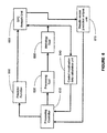
- An inner feedback loop is created between a processing controller 610, a processing tool 620, a metrology tool 630, and a control modification data calculation unit 640.
- the processing controller 610 is interfaced with the processing tool 620.
- the processing controller 610 calculates and sends control input signals that control the function of the processing tool 620.
- the processing tool 620 is interfaced with the metrology tool 630, which performs measurement of manufacturing parameters on semiconductor wafers that are processed by the processing tool 620.
- the metrology tool 630 is interfaced with the control modification data calculation unit 640.
- the control modification data calculation unit 640 uses data provided by the metrology tool 630 to perform calculations for the modification of control input signals that are generated by the processing controller 610.
- the control modification data calculation unit 640 is a computer program that is interfaced with the processing controller 610. Data from the control modification data calculation unit 640 is utilized by the processing controller 610 to modify control input signals that are sent to the processing tool 620 for a subsequent processing of semiconductor wafers.
- an outer feedback is created between the processing controller 610, the processing tool 620. the predictor function 650, the SPC analysis unit 660, and the results versus prediction analysis unit 670.
- the predictor function 650 is interfaced with the processing controller 610 and predicts an expected result of a manufacturing run of semiconductor wafers, based on the control input signals generated by the processing controller 610.
- the predictor function 650 is a computer program and is located within a manufacturing model 140. Data from the processed semiconductor wafers is used by the SPC analysis unit 660 to perform SPC analysis.
- the SPC analysis unit 660 is a computer program that is interfaced with the manufacturing model 140.
- the results versus prediction analysis unit 670 calculates the differences between the predicted results of a manufacturing run of semiconductor wafers and the actual results of a manufacturing run of semiconductor wafers.
- the results versus prediction analysis unit 670 is a computer program.
- the data calculated by the results versus prediction analysis unit 670 is used by the processing controller 610 to modify control input signals for a subsequent manufacturing run of semiconductor wafers that is performed by the processing tool 620.
- the principles taught by the present invention can be implemented into other types of manufacturing frameworks.
- the principles taught by the present invention can be implemented in an Advanced Process Control (APC) Framework.
- APC Advanced Process Control
- the APC is a preferred platform from which to implement the overlay control strategy taught by the present invention.
- the APC can be a factory-wide software system, therefore, the control strategies taught by the present invention can be applied to virtually any of the semiconductor manufacturing tools on the factory floor.
- the APC framework also allows for remote access and monitoring of the process performance. Furthermore, by utilizing the APC framework, data storage can be more convenient, more flexible, and less expensive than local drives.
- the APC platform allows for more sophisticated types of control because it provides a significant amount of flexibility in writing the necessary software code.
- Deployment of the control strategy taught by the present invention onto the APC framework could require a number of software components.
- a computer script is written for each of the semiconductor manufacturing tools involved in the control system.
- a semiconductor manufacturing tool in the control system When a semiconductor manufacturing tool in the control system is started in the semiconductor manufacturing fab, it generally calls upon a script to initiate the action that is required by the process controller, such as the overlay controller.
- the control methods are generally defined and performed in these scripts. The development of these scripts can comprise a significant portion of the development of a control system.
Landscapes
- Engineering & Computer Science (AREA)
- Manufacturing & Machinery (AREA)
- Automation & Control Theory (AREA)
- Quality & Reliability (AREA)
- Physics & Mathematics (AREA)
- General Physics & Mathematics (AREA)
- General Engineering & Computer Science (AREA)
- Computer Hardware Design (AREA)
- Microelectronics & Electronic Packaging (AREA)
- Power Engineering (AREA)
- General Factory Administration (AREA)
- Testing Or Measuring Of Semiconductors Or The Like (AREA)
- Feedback Control In General (AREA)
Description
Claims (10)
- A method for monitoring controller performance using statistical process control analysis, comprising:defining a manufacturing model (140);performing a processing run of semiconductor devices as defined by said manufacturing model (140) and implemented by a process controller (610);performing a fault detection analysis on said process controller (610); andupdating at least one control input signal generated by said process controller (610), said updating of said control input signal being modified based upon a multi-tier feedback structure, said multi-tier feedback structure comprising an inner feedback loop for detecting process errors and an outer feedback loop for performing said statistical process control analysis; andmodifying said manufacturing model (140) based on said updating of said control input signal.
- A method as claimed in claim 1, wherein performing a fault detection analysis on said process controller (610) further comprises:acquiring production data;performing process controller (610) performance monitoring using said production data;modifying said manufacturing model (140) in response to said process controller (610) performance monitoring; andimplementing said modified manufacturing model (140) in said process controller (610);
- A method as claimed in claim 2, wherein acquiring production data further comprises acquiring metrology data using a metrology tool (630).
- A method as claimed in claim 2 or claim 3, wherein performing process controller (610) performance monitoring using said production data further comprises:measuring manufacturing parameters;calculating modification data based upon said manufacturing parameters;performing statistical process control analysis;performing results versus prediction analysis based upon said statistical process control analysis; andmodifying said manufacturing model (140) based upon said calculated modification data and said results versus prediction analysis.
- A method as claimed in claim 4, wherein performing results versus prediction analysis further comprises comparing a predicted manufacturing process behavior to a result of a measured manufacturing process.
- An apparatus for monitoring controller performance using statistical process control analysis, the apparatus providing for a multi-tier feedback structure, said multi-tier feedback structure comprising an inner feedback loop for detecting process errors and an outer feedback loop for performing said statistical process control analysis, said apparatus comprising:a processing controller (610);a processing tool (620) coupled with said processing controller (610) ;a metrology tool (630) interfaced with said processing tool (620);a control modification data calculation unit (640) interfaced with said metrology and connected to said processing controller (610) in a feedback manner,a predictor function (650) interfaced with said processing controller (610) ;a statistical process control analysis unit (660) interfaced with said predictor function (650) and said processing tool (620); anda results versus prediction analysis unit (670) interfaced with said statistical process control analysis unit (660) and connected to said processing controller (610) in a feedback manner.
- An apparatus as claimed in claim 6, wherein said processing controller (610) is a run-to-run controller.
- An apparatus as claimed in claim 6, wherein said processing controller (610) is an automatic process control (APC) system.
- An apparatus as claimed in claim 6, 7 or 8, wherein said control modification data calculation unit (640) is a computer software program integrated into said processing controller (610).
- An apparatus for monitoring controller performance using statistical process control analysis, comprising:means for defining a manufacturing model (140);means for performing a processing run of semiconductor devices as defined by said manufacturing model (140) and implemented by a process controller (610);means for performing a fault detection analysis on said process controller (610) ;means for updating at least one control input signal generated by said process controller (610), said updating of said control input signal being modified based upon a multi-tier feedback structure, said multi-tier feedback structure comprising an inner feedback loop for detecting process errors and an outer feedback loop for performing said statistical process control analysis; andmeans for modifying said manufacturing model (140) based on said updating of said control input signal.
Applications Claiming Priority (3)
| Application Number | Priority Date | Filing Date | Title |
|---|---|---|---|
| US412679 | 1982-08-30 | ||
| US09/412,679 US6560503B1 (en) | 1999-10-05 | 1999-10-05 | Method and apparatus for monitoring controller performance using statistical process control |
| PCT/US2000/011522 WO2001025865A1 (en) | 1999-10-05 | 2000-04-28 | Method and apparatus for monitoring controller performance using statistical process control |
Publications (2)
| Publication Number | Publication Date |
|---|---|
| EP1218806A1 EP1218806A1 (en) | 2002-07-03 |
| EP1218806B1 true EP1218806B1 (en) | 2004-08-04 |
Family
ID=23633988
Family Applications (1)
| Application Number | Title | Priority Date | Filing Date |
|---|---|---|---|
| EP00928556A Expired - Lifetime EP1218806B1 (en) | 1999-10-05 | 2000-04-28 | Method and apparatus for monitoring controller performance using statistical process control |
Country Status (6)
| Country | Link |
|---|---|
| US (1) | US6560503B1 (en) |
| EP (1) | EP1218806B1 (en) |
| JP (1) | JP2003511750A (en) |
| KR (1) | KR100708009B1 (en) |
| DE (1) | DE60012762T2 (en) |
| WO (1) | WO2001025865A1 (en) |
Cited By (1)
| Publication number | Priority date | Publication date | Assignee | Title |
|---|---|---|---|---|
| WO2023039092A1 (en) * | 2021-09-10 | 2023-03-16 | Applied Materials, Inc. | Using elemental maps information from x-ray energy-dispersive spectroscopy line scan analysis to create process models |
Families Citing this family (35)
| Publication number | Priority date | Publication date | Assignee | Title |
|---|---|---|---|---|
| US20020049565A1 (en) * | 1998-03-19 | 2002-04-25 | Kirila Gene E. | Process and device to continuously monitor and control a manufacturing process |
| US6556884B1 (en) * | 2000-06-16 | 2003-04-29 | Advanced Micro Devices, Inc. | Method and apparatus for interfacing a statistical process control system with a manufacturing process control framework |
| US6725402B1 (en) | 2000-07-31 | 2004-04-20 | Advanced Micro Devices, Inc. | Method and apparatus for fault detection of a processing tool and control thereof using an advanced process control (APC) framework |
| US7123978B2 (en) * | 2000-12-27 | 2006-10-17 | Insyst Ltd. | Method for dynamically targeting a batch process |
| US7160739B2 (en) | 2001-06-19 | 2007-01-09 | Applied Materials, Inc. | Feedback control of a chemical mechanical polishing device providing manipulation of removal rate profiles |
| TW518645B (en) * | 2001-09-24 | 2003-01-21 | Powerchip Semiconductor Corp | Method and system of automatic wafer manufacture quality control |
| US8180587B2 (en) * | 2002-03-08 | 2012-05-15 | Globalfoundries Inc. | System for brokering fault detection data |
| US6772035B2 (en) * | 2002-05-17 | 2004-08-03 | Micron Technology, Inc. | Synthesizing semiconductor process flow models |
| US6925347B1 (en) * | 2002-08-19 | 2005-08-02 | Advanced Micro Devices, Inc. | Process control based on an estimated process result |
| DE10252605A1 (en) * | 2002-11-12 | 2004-06-24 | Infineon Technologies Ag | Method, device, computer-readable memory and computer program element for computer-aided monitoring and regulation of a manufacturing process |
| AU2003290932A1 (en) | 2002-11-15 | 2004-06-15 | Applied Materials, Inc. | Method, system and medium for controlling manufacture process having multivariate input parameters |
| US6941177B2 (en) * | 2002-12-17 | 2005-09-06 | Xerox Corporation | System and method for implementing real-time applications based on stochastic compute time algorithms |
| US7581140B1 (en) * | 2002-12-18 | 2009-08-25 | Advanced Micro Devices, Inc. | Initiating test runs based on fault detection results |
| US6912433B1 (en) * | 2002-12-18 | 2005-06-28 | Advanced Mirco Devices, Inc. | Determining a next tool state based on fault detection information |
| US7213478B2 (en) * | 2003-02-18 | 2007-05-08 | Tokyo Electron Limited | Method for automatic configuration of processing system |
| US8050900B2 (en) * | 2003-09-30 | 2011-11-01 | Tokyo Electron Limited | System and method for using first-principles simulation to provide virtual sensors that facilitate a semiconductor manufacturing process |
| US8036869B2 (en) * | 2003-09-30 | 2011-10-11 | Tokyo Electron Limited | System and method for using first-principles simulation to control a semiconductor manufacturing process via a simulation result or a derived empirical model |
| US8073667B2 (en) * | 2003-09-30 | 2011-12-06 | Tokyo Electron Limited | System and method for using first-principles simulation to control a semiconductor manufacturing process |
| US8032348B2 (en) * | 2003-09-30 | 2011-10-04 | Tokyo Electron Limited | System and method for using first-principles simulation to facilitate a semiconductor manufacturing process |
| US7010382B2 (en) * | 2004-02-26 | 2006-03-07 | Taiwan Semiconductor Manufacturing Co., Ltd. | Method and system for improving process control for semiconductor manufacturing operations |
| US6980873B2 (en) | 2004-04-23 | 2005-12-27 | Taiwan Semiconductor Manufacturing Company, Ltd. | System and method for real-time fault detection, classification, and correction in a semiconductor manufacturing environment |
| US7437404B2 (en) * | 2004-05-20 | 2008-10-14 | Taiwan Semiconductor Manufacturing Company, Ltd. | System and method for improving equipment communication in semiconductor manufacturing equipment |
| US8615314B1 (en) * | 2004-09-02 | 2013-12-24 | Advanced Micro Devices, Inc. | Process control using analysis of an upstream process |
| US7457729B2 (en) * | 2005-01-11 | 2008-11-25 | Verigy (Singapore) Pte. Ltd. | Model based testing for electronic devices |
| US8675176B2 (en) * | 2005-02-25 | 2014-03-18 | Asml Netherlands B.V. | Parameter control in a lithographic apparatus using polarization |
| US7117059B1 (en) * | 2005-04-18 | 2006-10-03 | Promos Technologies Inc. | Run-to-run control system and operating method of the same |
| KR100699856B1 (en) * | 2005-07-29 | 2007-03-27 | 삼성전자주식회사 | Control system for manufacturing of semiconductor device and method of controling using the same |
| US7720553B2 (en) * | 2006-08-31 | 2010-05-18 | Dell Products L.P. | Service metric portfolio management |
| US7974728B2 (en) | 2007-05-04 | 2011-07-05 | Taiwan Semiconductor Manufacturing Company, Ltd. | System for extraction of key process parameters from fault detection classification to enable wafer prediction |
| US7873585B2 (en) * | 2007-08-31 | 2011-01-18 | Kla-Tencor Technologies Corporation | Apparatus and methods for predicting a semiconductor parameter across an area of a wafer |
| US9760073B2 (en) * | 2010-05-21 | 2017-09-12 | Honeywell International Inc. | Technique and tool for efficient testing of controllers in development |
| TWI647630B (en) * | 2017-05-08 | 2019-01-11 | 萬泰科技股份有限公司 | Producing efficiency monitoring system |
| CN112074941A (en) | 2018-05-24 | 2020-12-11 | 应用材料公司 | Virtual sensor for spatially resolved wafer temperature control |
| KR102589004B1 (en) * | 2018-06-18 | 2023-10-16 | 삼성전자주식회사 | Semiconductor fualt analysis device and method for analyzing fault thereof |
| EP4012421A1 (en) * | 2020-12-11 | 2022-06-15 | Nxp B.V. | System and method for monitoring feedback circuits |
Family Cites Families (13)
| Publication number | Priority date | Publication date | Assignee | Title |
|---|---|---|---|---|
| JP2655904B2 (en) * | 1989-02-06 | 1997-09-24 | 三菱重工業株式会社 | Adaptive control device |
| JPH06244261A (en) * | 1990-12-31 | 1994-09-02 | Texas Instr Inc <Ti> | Sensor for controlling semiconductor device manufacturing process |
| US5257206A (en) * | 1991-04-08 | 1993-10-26 | Praxair Technology, Inc. | Statistical process control for air separation process |
| US5546312A (en) | 1993-09-20 | 1996-08-13 | Texas Instruments Incorporated | Use of spatial models for simultaneous control of various non-uniformity metrics |
| US5408405A (en) | 1993-09-20 | 1995-04-18 | Texas Instruments Incorporated | Multi-variable statistical process controller for discrete manufacturing |
| US5526293A (en) | 1993-12-17 | 1996-06-11 | Texas Instruments Inc. | System and method for controlling semiconductor wafer processing |
| US5452218A (en) | 1994-02-03 | 1995-09-19 | Texas Instruments | System and method for determining quality analysis on fabrication and/or assembly design using shop capability data |
| US5698455A (en) * | 1995-02-09 | 1997-12-16 | Micron Technologies, Inc. | Method for predicting process characteristics of polyurethane pads |
| US5659467A (en) * | 1996-06-26 | 1997-08-19 | Texas Instruments Incorporated | Multiple model supervisor control system and method of operation |
| KR19980026111A (en) * | 1996-10-07 | 1998-07-15 | 김광호 | Statistical Process Control Methods for Semiconductor Manufacturing |
| US5987398A (en) | 1998-04-30 | 1999-11-16 | Sony Corporation | Method and apparatus for statistical process control of machines and processes having non-constant mean of a response variable |
| US6230069B1 (en) | 1998-06-26 | 2001-05-08 | Advanced Micro Devices, Inc. | System and method for controlling the manufacture of discrete parts in semiconductor fabrication using model predictive control |
| US6298470B1 (en) * | 1999-04-15 | 2001-10-02 | Micron Technology, Inc. | Method for efficient manufacturing of integrated circuits |
-
1999
- 1999-10-05 US US09/412,679 patent/US6560503B1/en not_active Expired - Fee Related
-
2000
- 2000-04-28 DE DE60012762T patent/DE60012762T2/en not_active Expired - Lifetime
- 2000-04-28 WO PCT/US2000/011522 patent/WO2001025865A1/en active IP Right Grant
- 2000-04-28 KR KR1020027004424A patent/KR100708009B1/en not_active IP Right Cessation
- 2000-04-28 JP JP2001528761A patent/JP2003511750A/en active Pending
- 2000-04-28 EP EP00928556A patent/EP1218806B1/en not_active Expired - Lifetime
Cited By (1)
| Publication number | Priority date | Publication date | Assignee | Title |
|---|---|---|---|---|
| WO2023039092A1 (en) * | 2021-09-10 | 2023-03-16 | Applied Materials, Inc. | Using elemental maps information from x-ray energy-dispersive spectroscopy line scan analysis to create process models |
Also Published As
| Publication number | Publication date |
|---|---|
| US6560503B1 (en) | 2003-05-06 |
| KR20020047215A (en) | 2002-06-21 |
| DE60012762T2 (en) | 2005-08-11 |
| KR100708009B1 (en) | 2007-04-16 |
| WO2001025865A1 (en) | 2001-04-12 |
| EP1218806A1 (en) | 2002-07-03 |
| DE60012762D1 (en) | 2004-09-09 |
| JP2003511750A (en) | 2003-03-25 |
Similar Documents
| Publication | Publication Date | Title |
|---|---|---|
| EP1218806B1 (en) | Method and apparatus for monitoring controller performance using statistical process control | |
| US6556884B1 (en) | Method and apparatus for interfacing a statistical process control system with a manufacturing process control framework | |
| US6442496B1 (en) | Method and apparatus for dynamic sampling of a production line | |
| US6465263B1 (en) | Method and apparatus for implementing corrected species by monitoring specific state parameters | |
| US6304999B1 (en) | Method and apparatus for embedded process control framework in tool systems | |
| US6622061B1 (en) | Method and apparatus for run-to-run controlling of overlay registration | |
| US8676538B2 (en) | Adjusting weighting of a parameter relating to fault detection based on a detected fault | |
| US6248602B1 (en) | Method and apparatus for automated rework within run-to-run control semiconductor manufacturing | |
| US6449524B1 (en) | Method and apparatus for using equipment state data for run-to-run control of manufacturing tools | |
| US6773931B2 (en) | Dynamic targeting for a process control system | |
| US6484064B1 (en) | Method and apparatus for running metrology standard wafer routes for cross-fab metrology calibration | |
| US6427093B1 (en) | Method and apparatus for optimal wafer-by-wafer processing | |
| US6405144B1 (en) | Method and apparatus for programmed latency for improving wafer-to-wafer uniformity | |
| US6647309B1 (en) | Method and apparatus for automated generation of test semiconductor wafers | |
| US6532428B1 (en) | Method and apparatus for automatic calibration of critical dimension metrology tool | |
| US6560506B2 (en) | Method and apparatus for control for semiconductor processing for reducing effects of environmental effects | |
| US6947803B1 (en) | Dispatch and/or disposition of material based upon an expected parameter result | |
| US6834213B1 (en) | Process control based upon a metrology delay | |
| US6571371B1 (en) | Method and apparatus for using latency time as a run-to-run control parameter | |
| US6871114B1 (en) | Updating process controller based upon fault detection analysis | |
| US6834211B1 (en) | Adjusting a trace data rate based upon a tool state | |
| US6788988B1 (en) | Method and apparatus using integrated metrology data for pre-process and post-process control | |
| US6912436B1 (en) | Prioritizing an application of correction in a multi-input control system | |
| US6549822B1 (en) | Method and apparatus for control of multi-cup semiconductor manufacturing tracks | |
| US7120514B1 (en) | Method and apparatus for performing field-to-field compensation |
Legal Events
| Date | Code | Title | Description |
|---|---|---|---|
| PUAI | Public reference made under article 153(3) epc to a published international application that has entered the european phase |
Free format text: ORIGINAL CODE: 0009012 |
|
| 17P | Request for examination filed |
Effective date: 20020327 |
|
| AK | Designated contracting states |
Kind code of ref document: A1 Designated state(s): AT BE CH CY DE DK ES FI FR GB GR IE IT LI LU MC NL PT SE |
|
| AX | Request for extension of the european patent |
Free format text: AL;LT;LV;MK;RO;SI |
|
| GRAP | Despatch of communication of intention to grant a patent |
Free format text: ORIGINAL CODE: EPIDOSNIGR1 |
|
| GRAS | Grant fee paid |
Free format text: ORIGINAL CODE: EPIDOSNIGR3 |
|
| GRAA | (expected) grant |
Free format text: ORIGINAL CODE: 0009210 |
|
| AK | Designated contracting states |
Kind code of ref document: B1 Designated state(s): DE GB |
|
| REG | Reference to a national code |
Ref country code: GB Ref legal event code: FG4D |
|
| REG | Reference to a national code |
Ref country code: IE Ref legal event code: FG4D |
|
| REF | Corresponds to: |
Ref document number: 60012762 Country of ref document: DE Date of ref document: 20040909 Kind code of ref document: P |
|
| LTIE | Lt: invalidation of european patent or patent extension |
Effective date: 20040804 |
|
| PLBE | No opposition filed within time limit |
Free format text: ORIGINAL CODE: 0009261 |
|
| STAA | Information on the status of an ep patent application or granted ep patent |
Free format text: STATUS: NO OPPOSITION FILED WITHIN TIME LIMIT |
|
| 26N | No opposition filed |
Effective date: 20050506 |
|
| REG | Reference to a national code |
Ref country code: GB Ref legal event code: 732E Free format text: REGISTERED BETWEEN 20091210 AND 20091216 |
|
| PGFP | Annual fee paid to national office [announced via postgrant information from national office to epo] |
Ref country code: GB Payment date: 20100312 Year of fee payment: 11 |
|
| PGFP | Annual fee paid to national office [announced via postgrant information from national office to epo] |
Ref country code: DE Payment date: 20110429 Year of fee payment: 12 |
|
| GBPC | Gb: european patent ceased through non-payment of renewal fee |
Effective date: 20110428 |
|
| PG25 | Lapsed in a contracting state [announced via postgrant information from national office to epo] |
Ref country code: GB Free format text: LAPSE BECAUSE OF NON-PAYMENT OF DUE FEES Effective date: 20110428 |
|
| REG | Reference to a national code |
Ref country code: DE Ref legal event code: R119 Ref document number: 60012762 Country of ref document: DE Effective date: 20121101 |
|
| PG25 | Lapsed in a contracting state [announced via postgrant information from national office to epo] |
Ref country code: DE Free format text: LAPSE BECAUSE OF NON-PAYMENT OF DUE FEES Effective date: 20121101 |