EP1172733B1 - Method and apparatus for transmitting control information across a serialized bus interface - Google Patents
Method and apparatus for transmitting control information across a serialized bus interface Download PDFInfo
- Publication number
- EP1172733B1 EP1172733B1 EP01000297.0A EP01000297A EP1172733B1 EP 1172733 B1 EP1172733 B1 EP 1172733B1 EP 01000297 A EP01000297 A EP 01000297A EP 1172733 B1 EP1172733 B1 EP 1172733B1
- Authority
- EP
- European Patent Office
- Prior art keywords
- interface device
- coupled
- bus
- reset
- control
- Prior art date
- Legal status (The legal status is an assumption and is not a legal conclusion. Google has not performed a legal analysis and makes no representation as to the accuracy of the status listed.)
- Expired - Lifetime
Links
Images

Classifications
-
- G—PHYSICS
- G06—COMPUTING; CALCULATING OR COUNTING
- G06F—ELECTRIC DIGITAL DATA PROCESSING
- G06F13/00—Interconnection of, or transfer of information or other signals between, memories, input/output devices or central processing units
- G06F13/38—Information transfer, e.g. on bus
- G06F13/40—Bus structure
- G06F13/4004—Coupling between buses
- G06F13/4027—Coupling between buses using bus bridges
- G06F13/4045—Coupling between buses using bus bridges where the bus bridge performs an extender function
Definitions
- This invention relates generally to computer systems and components and specifically to a method and apparatus for transmitting control information across a serialized bus interface.
- PCI Peripheral Component Interface
- ISA Industry Standard Architecture
- EISA Extended Industry Standard Architecture
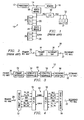
- FIG. 1 illustrates a block diagram of a conventional computer system 10.
- Processor 12 may be an x86 compatible microprocessor such as the Pentium (II or III) available from Intel Corporation or the equivalent processor (e.g., K6 or K7) available from Advanced Micro Devices.
- processor e.g., K6 or K7
- the processor 12 is coupled to a processor bus 14, which is typically proprietary (e.g., not standardized) to the processor 12.
- the bus 14 is coupled to a memory system 16.
- the memory system 16 includes dynamic random access memory (DRAM) as well as associated control circuitry.
- DRAM dynamic random access memory
- Processor bus 14 is also coupled to a PCI bus 20 through a bridge circuit 18, often referred to as a north bridge.
- a bridge circuit 18 often referred to as a north bridge.
- the memory control circuitry from memory system 16 and the bridge circuitry are combined in a single chip.
- the north bridge 18 would be coupled between processor 12 and memory 16.
- PCI bus 20 includes a number of slots 22 that can be used to couple various devices to the bus.
- the slots could be used to coupled devices such as hard disk drives, modems, network interface cards, optical drives (e.g., CD ROM or DVD), or other devices.
- PCI bus 20 is coupled to a legacy bus, typically an ISA or EISA bus 26, through a second bridge circuit 24, often referred to as a south bridge.
- the (E)ISA bus 26 includes slots 28 typically used for input/output devices such as the keyboard, mouse, display and other devices such as the non-volatile memory.
- the PCI bus 20 is a standardized bus and therefore can include only a limited number of slots 22. If more slots are needed, a second PCI bus 32 can be coupled to the first PCI bus 20 through a PCI-to-PCI bridge circuit (P2P) 30.
- P2P PCI-to-PCI bridge circuit
- the PCI bus 20 coupled to the north bridge is referred to as the primary PCI bus and the second PCI bus 32 is referred to as the secondary PCI bus.
- the secondary PCI bus 32 includes slots 34 that can be utilized in the same manner as slots 22. In fact, from the perspective of an operating system being executed on processor 12 primary PCI bus 20 and secondary PCI bus 32 appear to be a single PCI bus.
- European Patent Application No. 0923035 describes an encoder in which detection of a block code boundary and the re-establishment of synchronization between a scrambler and a descrambler can be performed.
- An acknowledgment that a bus reset is output from a transmitting side using a signal that is not randomized to the receiving side and the initiation of the network and the initiation of the serial port can be performed at the same time using a bus reset signal.
- the present invention provides a method of communicating from a processor to a peripheral device, a bus interface device and a computer system incorporating the bus interface device as set out in the appended claims.
- the preferred embodiment present invention provides a scheme that can be used to transmit control signal from one parallel bus to a second parallel bus over a serial link. While not limited to a single type of system, the preferred embodiment of the present invention was developed initially in the context of a PCI-to-PCI bridge that includes a serial link. This type of configuration provides advantages in a number of situations such as when the secondary PCI bus is separated from the primary PCI bus.
- a serial PCI-to-PCI bridge is different from a conventional PCI-to-PCI bridge in the respect that it has a serial link between the two PCI interfaces.
- Each PCI interface is typically a separate entity or a separate chip. Both the interface chips can communicate between them in two modes of operation through the serial link.
- One problem addressed by the preferred embodiment involves resetting the secondary PCI interface device and another is initializing both the parts to the same mode so that they can start communicating data between them.
- the present invention will be described in the context of a specific example, namely a PCI-to-PCI bridge.
- a unique computer system can be derived.
- This system can be useful in a number of specific applications such as with a portable computer/docking station, small form factor PC expansion and in telecommunications environments. Other applications and embodiments can also be utilized.
- a PCI-to-PCI bridge 30 is a link between a primary PCI bus 20 and a secondary PCI bus 32.
- a conventional PCI-to-PCI bridge 30, illustrated in Figure 2 is formed from a single chip, i.e., a single piece of silicon. As shown in the figure, this device can be logically divided between a primary side 36 and a secondary side 38. The primary side 36 is the interface to the primary PCI bus 20 and the secondary side 38 of the P2P 30 is the interface to the secondary PCI bus 32.
- the PCI-to-PCI bridge 30 follows the PCI bridge protocol to transfer data between the two buses 20 and 32.
- the primary side 36 can set the secondary side 38 to different states or modes of operation depending on the need of the system. When it is needed to set the secondary side 38 to the initial state, the primary side 36 can issue a signal called RESET to the secondary side 38 thereby causing the secondary side 38 to enter the initial state.
- RESET signal on the PCI bridge's secondary side 38 can be asserted under certain conditions.
- the bridge 30 When the primary PCI bus 20 wants to bring the bridge 30 to its initial state and issues a RESET signal to primary side 36 of the bridge 30, the bridge 30 must assert RESET on the secondary side 38 as well. This action will initialize the entire bus 20/32 to the initial state. In another instance, the bridge 30 asserts RESET on the secondary side 38 whenever software sets the SECONDARY BUS RESET bit in the bridge's bridge control register.
- the bridge 30 may also need to initialize the secondary side 38 and assert RESET under certain other conditions. For example, when the system 10 is powered on, it may want to bring all the components in the system to an initial state and issue a RESET to all the components as a global reset. This global reset needs to be communicated to the secondary side 38. In another situation during the operation of the bridge 30, it may be desirable to bring the secondary side 32 to the initial state before transitioning to a next phase of operation. The bridge 32 may also need to reset the secondary bus 32 if there is a change in the mode of power states.
- the reset signal For conventional bridges it is easy to convey the reset signal from the primary side 36 to the secondary side 38 because both the sides remain in the same chip. So, a signal can be generated from the primary side 36 for the above conditions and the information can be transferred to the secondary easily.
- the transfer might be as simple as routing a line of metal across the chip and gating that line appropriately.
- the preferred embodiment of the present invention deals with a split PCI-to-PCI bridge.
- the primary side and the secondary side of the PCI-to-PCI bridge are formed in separate devices, e.g., separate pieces of silicon that are coupled together, in this case by a serial link.
- a metal line over the substrate to provide control signals from the primary side to the secondary side.
- the preferred embodiment of the present invention provides a PCI interface device (52 or 58 in Figure 3 ) that can serve as a half PCI bridge.
- This device can be used either as a primary or a secondary part of a bridge.
- As a primary interface device it is coupled to the primary PCI bus 20 and as a secondary interface device it is coupled to the secondary PCI bus 32.
- FIG. 3 illustrates a PCI-to-PCI bridge 50 of the present invention.
- the PCI-to-PCI bridge 50 is formed from four chips.
- the primary interface device 52 is coupled to the secondary interface 58 through a serial link 60.
- the serial link 60 is accessed by transceiver, e.g., serializer/deserializer, devices 54 and 56.
- transceiver e.g., serializer/deserializer, devices 54 and 56.
- the present invention contemplates an embodiment where the primary interface 52 and the transceiver 54 are combined into a single device and the secondary interface 58 and the transceiver 56 are combined into another single device.
- the system is fully symmetric so that either PCI bus could be the primary bus.
- the interface devices 52 and 58 and the transceivers 54 and 56 may include substantially identical circuitry.
- serial link 60 is a single-channel, bi-directional, point-to-point interface.
- serial link 60 comprises a differential pair of wires for communication from transceiver 54 to transceiver 56 and a second differential pair of wires for communication from transceiver 56 to transceiver 54.
- Single-ended wires could alternatively be used. Data signals and control signals share the same line.
- the system's coding scheme is used to differentiate data from control. This type of configuration is convenient since it can utilize a standard category 5 cable, such as the cables used in regular Ethernet applications.
- the invention could be implemented with a single differential pair or single-ended wire in a half duplex system.
- interface devices 52 and 58 are coupled together by a pair of serializer/deserializer devices 54/56 used for ultra high speed bi-directional point-to-point data transmissions.
- the serializer/deserializer devices 54 and 56 are TLK2500 transceivers available from Texas Instruments Incorporated.
- the TLK2500 has a fixed number of pins and a predetermined modes of operation.
- the reset information from primary interface device 52 to secondary interface device 58 needs to be communicated through both the transceivers 54 and 56. Unfortunately, there is no direct way to communicate the reset signal to the secondary from the primary side.
- the data transfer between a primary 52 and a secondary 58 interface device can occur in more than one mode.
- data transfer can occur in either CRC (cyclic redundancy code) mode or non-CRC mode.
- CRC cyclic redundancy code
- non-CRC non-CRC mode
- both the interface devices 52 and 58 should be in the same data transfer mode for proper recognition of data packets.
- the secondary interface device 58 should also change to the same mode for proper data communication.
- the secondary side 58 should be set to initial state after each change in CRC mode before proper transaction of data can be made.
- the present invention provides a technique to communicate a RESET signal in a proper fashion not only to set the secondary interface device 58 to an initial state but also to set the mode of transaction between two interface devices 52 and 58.
- RESET goes active, a pattern of signals is sent from the primary device 52 to the secondary device 58 using the control lines of transceivers 54 and 56. In this manner, the system takes advantage of control codes provided by the line coding system.
- transceivers 54 and 56 might utilize a 8B/10B encoding and decoding scheme.
- IEEE Standard 802.3, ⁇ 36.2.4 provides details of the 8B/10B code.
- This encoding/decoding scheme can be implemented on-chip with the TLK2500.
- the encoding scheme has predetermined control codes that are distinguishable from data codes.
- the serial link 60 can be driven with these codes to communicate the RESET from the primary interface device 52 to the secondary interface device 58.
- the reset and mode information can be communicated independent of user data.
- Different side-band signals can also be communicated from primary side 52 to secondary side 58 with this procedure. Different patterns can be inserted to communicate different signals and different headers can be used to make different groups of signals. So, any bit in a secondary side register or a primary side register can be set or read from the other side and the signals could be communicated to the proper input, output or the internal circuitry.
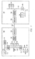
- FIG. 4 illustrates a specific example that utilizes aspects of the present invention.
- This embodiment includes circuitry within the interface devices 52 and 58 that can be used to communicate control information between these two devices. This circuitry helps to keep the interface devices in the same CRC mode of operation and communicate the RESET signal from primary interface device 52 to secondary interface device 58 through both the transceivers 54 and 56 as shown in Figure 4 .
- the implementation of Figure 4 is based on the TLK2500.
- the TLK2500 performs data parallel-to-serial, serial-to-parallel, and clock extraction functions for a physical layer interface device.
- the parallel data is internally encoded using an 8B/10B encoding format.
- the resulting work can then be transmitted differentially at a high speed reference clock rate.
- the device also includes a receiver section that performs serial-to-parallel conversion on the input data synchronizing the received data to an extracted reference clock. It then decides the data using 8B/10B decoding format to derive the original parallel data.
- the interface 52 or 58 to the TLK2500 is 16 bits wide and operates at 125 MHz. This interface has a raw throughput of 250 million bytes per second.
- the transmit data rate from interface 52 or 58 to TLK2500 is the same as the receive data rate from the TLK2500 to interface 52 or 58.
- the interface 52 or 58 to the PCI bus operates at 33 MHz and is 32 bits wide. That PCI interface has a raw throughput of 133 million bytes per second.
- the excess throughput on the TLK2500 interface is used up in packet overhead, CRC codes, protocol delays, etc. Based upon simulations, the combined link can sustain about 120 million bytes per second for an extended period.
- the PCI bus specification also permits higher speeds, up to 66 MHz and wider widths, up to 64 bits wide. That would require about four times the throughput on the TLK2500 link.
- the present invention contemplates an embodiment that supports this kind of high speed bus by a combination of faster clock rates on the high speed serial data and/or running several high speed serial channels in parallel.
- the Reset/CRC protocols operate at a at the high speed clock rates rather that at the PCI clock rates.
- the advantage is that they operate faster, allowing faster error recovery and/or faster mode changes than a pure PCI-based implementation.
- the TLK2500 includes an 8B/10B encoder that converts 8 bit wide data to a 10 bit wide encoded data character to improve its transmission characteristics. Since the TLK2500 is a 16 bit wide interface the data is split into two 8-bit wide bytes for encoding. Each byte is fed into a separate encoder.
- the data transfer through the TLK2500 depends on four control pins. These pins are called TX_EN (transmit enable), TX_ER (transmits error coding), RX_DV (receive data valid) and RX_ER (receive error).
- the device also has 32 data pins, TXD[0:15] (transmit data) and RXD[0:15] (receive data).
- TXD pins are used to receive the transmitted data in the other interface device with the control pins RX_DV and RX_ER.
- TX_EN and TX_ER pins are replicated in the receive side in RX_DV and RX_ER pins.
- the control pins TX_EN and TX_ER can have four states, which are indicated in Table 1.
- Table 1 TX_EN/RX_DV TX_ER/RX_ER 8B/10B Codes State 0 0 ⁇ K28.5, D5.6> ⁇ K28.5, D16.2> Idle 0 1 ⁇ K23.7> Carrier Extend 1 0 ⁇ Dxx.y> Normal Data 1 1 ⁇ K30.7> Error
- the four states are Idle, Carrier Extend, Normal data and Error.
- TX_EN and TX_ER are put into Normal Data mode, TX_EN is high and TX_ER is low.
- the data in TXD pins are accepted in one transceiver 54 (56) and the data is produced in the RXD pins of the other transceiver 56 (54) with the RX_DV and RX_ER showing Normal Data mode. So, there is data transmission between the interface devices 52 and 58 through the two transceivers 54 and 56 in Normal Data mode.
- the transceiver 54 does not accept data from TXD pins but sends its own special data and produces the data in the RXD pins of the other transceiver 56 (54) with the same state of TX_EN and TX_ER in RX_DV and RX_ER.
- TX_EN is deasserted and TX_ER is asserted
- the encoder will generate a carrier extend consisting of two K23.7 codes. If TX_EN and TX_ER are both asserted then the encoder will generate a special event.
- This special event comprises one or more code-groups that are not part of the valid data or delimiter set somewhere in the frame being transmitted. In the preferred embodiment, this special event is a K30.7 code, which is the last of the control codes defined in the 8b10b specification. This code does not provide a comma pattern, so it does not define the byte boundary in the data stream.
- IDLE comprises a K28.5 code and either a D5.6 or D16.2 character. Since data is latched into the TLK2500 16 bits at a time, this in turn is converted into two 10-bit codes that are transmitted sequentially. This means IDLE will comprise two 10 bit codes, being 20 bits wide that is transmitted during a single cycle. IDLE will replace data during initial synchronization or resynchronization, until synchronization is achieved.
- the primary device 52 When a reset from the primary interface device 52 needs to be communicated to the secondary side 58, the primary device 52 communicates this reset to a communication control circuitry block with the interface device 52.
- the control block takes control of the serial link 60 and sends a unique pattern of Extends and Idles through TX_EN and TX_ER, depending on the CRC mode of the primary side.
- FIG. 5 shows a complete reset procedure.
- UUT0 represents the signals from primary interface device 52 and UUT1 represents signals from secondary interface device 58.
- UUT stands for Unit Under Test.
- the reset procedure starts if UUT0:SERIAL_RST is set high.
- UUT0:PCI_RST_L is an external reset signal to the primary device 52 which signals set when it is low. This signal causes UUT0:SERIAL_RST to go high.
- UUT0:TX_EN When there is a reset, UUT0:TX_EN signal will go low and UUT0:TX_ER signal will toggle to send Extends and Idles.
- An Idle is signaled if both the TX_ER and TX_EN is low and an Extend is signaled when TX_ER is high and TX_EN is low.
- the pattern sent from primary device 52 is replicated in UUT1:RX_DV and UUT1:RXER_PASS of the secondary device 58.
- RXER_PASS is an input pin of the interface device 52 (58) that is connected to the RX_ER pin of the transceiver 54 (56).
- the UUT1:XMT_EN transmit enable
- the UUT1:XMT_EN transmit enable
- RCVD_SEC_DPATH_RST goes low
- XMT_EN disables normal operation and starts the RESET procedure.
- UUT1:RXER_PASS goes low after the final Extend, several clock cycles later, a confirmation pattern is produced in UUT1:TX_EN and UUT1:TX_ER which is passed to UUT0:RX_DV and UUT0:RXER_PASS as a confirmation of RESET.
- the reset procedure completes; XMT_EN in both primary and second devices goes high. If the primary device 52 does not get back the confirmation within certain time due to the error in the link (or any other reason), the control block in the primary device 52 tries to send reset again. In this manner, the system is more robust.
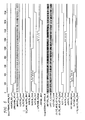
- the reset pattern comprises three parts, namely a header, mode information and a tail.
- the header comprises three Extends, three Idles and three Extends again.
- the mode information part comprises three sets of three Extends and Idles for the CRC Mode or three sets of three Idles and Extends for Non-CRC mode (see Table 2).
- the tail part consists of sixty-eight Extends. The tail part can be made to have a variable extend, so that it will transmit extends as long as there is a reset in the primary.
- One advantage of the preferred embodiment implementation is that all the Extends and Idles in the reset pattern are more than one clock cycle wide. This feature helps to avoid an erroneous reset in the secondary side due to any misleading spikes in the link.
- the confirmation pattern is same as the reset pattern except that the mode information bits are reversed and its tail is only three Extends wide. It is preferable that the mode information be inverted for the confirmation so that any electro-magnetic crosstalk that might occur between the two lines in link 60 will not be confused for a confirmation. With this technique, echo on the line will not be misinterpreted as a confirmation.
- the reset procedure can been done without the reset confirmation.
- This embodiment is not preferred, however, since it might mislead to a secondary reset due to a breakdown in the serial link.
- the bits in the confirmation packets can be kept in the same pattern as the reset pattern but this approach might not catch the signals that have been induced in the high speed domain (e.g., crosstalk).
- Figure 6 shows a timing diagram for the non-CRC mode.
- PCI_RST_L is high, but an internal reset, a pulse in SERIAL_RST, occurs in the primary interface device 52, which causes the reset procedure.
- the CRC mode signal CRC_EN in the primary side goes to low indicating that communication is to occur in the Non-CRC mode.
- the reset procedure makes a similar change in the secondary interface device 58 by changing the signal SEC_CRC_EN from high to low. A different pattern is communicated during this reset to show the Non-CRC mode of operation.
- the mode information part of the packet includes Idles followed by Extends to indicate Non-CRC mode.
- Table 2 summarizes the reset pattern for both the CRC and non-CRC modes.
- Table 2 Redundancy Mode To/From Header Mode Information Tail CRC Mode Primary/Secondary EIE EIEIEI EEE ... EE
- CRC confirm Secondary/Primary EIE IEIEIE EEE Non-CRC Mode Primary/Secondary EIE IEIEIE EEE ... EE
- Non-CRC confirm Secondary/Primary EIE EIEI EEE
- Figure 7 illustrates a block diagram of a portable (e.g., notebook or handheld) computer 102 and an associated docking station 104.
- the portable computer 102 can be coupled to the docking station 104 using a category 5 cable 60. This simple plug-in connection is convenient and reliable.
- the computer system 102 includes microprocessor 112 which is coupled to memory system 116 and north bridge 118.
- Primary PCI bus 120 includes a number of slots for connection of components such as hard disk drives, modems, CD ROM drives, DVD drives and network interface cards, as examples.
- South bridge 124 is provided for access to a different bus, e.g., (E)ISA bus, 126, which may have other components coupled to it.
- E EISA bus
- primary PCI bus 120 also includes a primary interface device 152, as described above.
- the primary interface device 152 is coupled to transceiver 154, which serializes the parallel data from PCI bus 120 and transmits it across serial link 160.
- the serial data is received at transceiver 156 and returned to parallel data to be transferred to secondary interface device 158.
- Data and control signals can further be transmitted in the opposite direction, that is from secondary side 158 to primary side 152.
- Figure 7 further illustrates a third PCI bus 172 that is coupled to secondary bus 132 through a PCI-to-PCI bridge 170.
- the PCI-to-PCI bridge 170 can be a conventional single chip device as illustrated in Figure 7 or a serialized device such as illustrated in Figure 3 or Figure 4 . In the latter case, the docking station 104 could be further coupled to a remote expansion box via a cable, as one example.
- the reset signal and mode information are communicated from one PCI bus to the other using control space of the coding scheme.
- This provides advantages over alternate schemes.
- the reset signal could have been included in the PCI data packets instead of a completely separate circuit block handling the reset procedure.
- This approach will tend to complicate the mode set procedure.
- this approach can be used in other designs for the similar kind of reset procedures through a serial link. Since the system can communicate the reset signal independent of other blocks of the design, it helps in modular design.
- FIG. 7 The block diagram of Figure 7 can also be utilized in other systems. For example, small-form-factor computers do not have room for much expansion. A cable interfaced to the exterior of the computer can be coupled to an expansion box that includes additional cards. Similarly, other computers that require remote expansion can utilize the benefits of the present invention.
Landscapes
- Engineering & Computer Science (AREA)
- General Engineering & Computer Science (AREA)
- Theoretical Computer Science (AREA)
- Computer Hardware Design (AREA)
- Physics & Mathematics (AREA)
- General Physics & Mathematics (AREA)
- Information Transfer Systems (AREA)
- Bus Control (AREA)
- Small-Scale Networks (AREA)
Description
- This invention relates generally to computer systems and components and specifically to a method and apparatus for transmitting control information across a serialized bus interface.
- Computer system architectures are typically designed with standardized busses that can include slots. Various devices can be coupled to the system via these slots. Examples of standardized busses include the Peripheral Component Interface (PCI) bus, the Industry Standard Architecture (ISA) bus and the Extended Industry Standard Architecture (EISA) bus.
-
Figure 1 illustrates a block diagram of a conventional computer system 10.Processor 12 may be an x86 compatible microprocessor such as the Pentium (II or III) available from Intel Corporation or the equivalent processor (e.g., K6 or K7) available from Advanced Micro Devices. - The
processor 12 is coupled to aprocessor bus 14, which is typically proprietary (e.g., not standardized) to theprocessor 12. Thebus 14 is coupled to amemory system 16. Thememory system 16 includes dynamic random access memory (DRAM) as well as associated control circuitry. -
Processor bus 14 is also coupled to aPCI bus 20 through abridge circuit 18, often referred to as a north bridge. In some instances, the memory control circuitry frommemory system 16 and the bridge circuitry are combined in a single chip. In this case, not illustrated, thenorth bridge 18 would be coupled betweenprocessor 12 andmemory 16. -
PCI bus 20 includes a number ofslots 22 that can be used to couple various devices to the bus. For example, the slots could be used to coupled devices such as hard disk drives, modems, network interface cards, optical drives (e.g., CD ROM or DVD), or other devices. -
PCI bus 20 is coupled to a legacy bus, typically an ISA or EISAbus 26, through asecond bridge circuit 24, often referred to as a south bridge. The (E)ISAbus 26 includesslots 28 typically used for input/output devices such as the keyboard, mouse, display and other devices such as the non-volatile memory. - The
PCI bus 20 is a standardized bus and therefore can include only a limited number ofslots 22. If more slots are needed, asecond PCI bus 32 can be coupled to thefirst PCI bus 20 through a PCI-to-PCI bridge circuit (P2P) 30. In this configuration, thePCI bus 20 coupled to the north bridge is referred to as the primary PCI bus and thesecond PCI bus 32 is referred to as the secondary PCI bus. Thesecondary PCI bus 32 includesslots 34 that can be utilized in the same manner asslots 22. In fact, from the perspective of an operating system being executed onprocessor 12primary PCI bus 20 andsecondary PCI bus 32 appear to be a single PCI bus. - European Patent Application No.
0923035 describes an encoder in which detection of a block code boundary and the re-establishment of synchronization between a scrambler and a descrambler can be performed. An acknowledgment that a bus reset is output from a transmitting side using a signal that is not randomized to the receiving side and the initiation of the network and the initiation of the serial port can be performed at the same time using a bus reset signal. - The present invention provides a method of communicating from a processor to a peripheral device, a bus interface device and a computer system incorporating the bus interface device as set out in the appended claims.
- The preferred embodiment present invention provides a scheme that can be used to transmit control signal from one parallel bus to a second parallel bus over a serial link. While not limited to a single type of system, the preferred embodiment of the present invention was developed initially in the context of a PCI-to-PCI bridge that includes a serial link. This type of configuration provides advantages in a number of situations such as when the secondary PCI bus is separated from the primary PCI bus.
- A serial PCI-to-PCI bridge is different from a conventional PCI-to-PCI bridge in the respect that it has a serial link between the two PCI interfaces. Each PCI interface is typically a separate entity or a separate chip. Both the interface chips can communicate between them in two modes of operation through the serial link. One problem addressed by the preferred embodiment involves resetting the secondary PCI interface device and another is initializing both the parts to the same mode so that they can start communicating data between them.
- The present invention will now be further described by way of example, with reference to the preferred and exemplary embodiments illustrated in the figures of the accompanying drawings in which:
-
Figure 1 is a block diagram of a conventional computer system; -
Figure 2 is a block diagram of a conventional PCI-to-PCI bridge; -
Figure 3 is a block diagram of a PCI-to-PCI bridge; -
Figure 4 is a block diagram of a more specific PCI-to-PCI bridge; -
Figures 5 and6 are timing diagrams illustrating the operation; and -
Figure 7 is a block diagram of a computer system. - The making and use of the various embodiments are discussed below in detail. However, it should be appreciated that the present invention provides many applicable inventive concepts which can be embodied in a wide variety of specific contexts. The specific embodiments discussed are merely illustrative of specific ways to make and use the invention, and do not limit the scope of the invention.
- The present invention will be described in the context of a specific example, namely a PCI-to-PCI bridge. When utilized in this manner, a unique computer system can be derived. This system can be useful in a number of specific applications such as with a portable computer/docking station, small form factor PC expansion and in telecommunications environments. Other applications and embodiments can also be utilized.
- Referring back to prior art
Figure 1 , a PCI-to-PCI bridge 30 is a link between aprimary PCI bus 20 and asecondary PCI bus 32. A conventional PCI-to-PCI bridge 30, illustrated inFigure 2 , is formed from a single chip, i.e., a single piece of silicon. As shown in the figure, this device can be logically divided between aprimary side 36 and asecondary side 38. Theprimary side 36 is the interface to theprimary PCI bus 20 and thesecondary side 38 of theP2P 30 is the interface to thesecondary PCI bus 32. - The PCI-to-
PCI bridge 30 follows the PCI bridge protocol to transfer data between the twobuses primary side 36 can set thesecondary side 38 to different states or modes of operation depending on the need of the system. When it is needed to set thesecondary side 38 to the initial state, theprimary side 36 can issue a signal called RESET to thesecondary side 38 thereby causing thesecondary side 38 to enter the initial state. The RESET signal on the PCI bridge'ssecondary side 38 can be asserted under certain conditions. - When the
primary PCI bus 20 wants to bring thebridge 30 to its initial state and issues a RESET signal toprimary side 36 of thebridge 30, thebridge 30 must assert RESET on thesecondary side 38 as well. This action will initialize theentire bus 20/32 to the initial state. In another instance, thebridge 30 asserts RESET on thesecondary side 38 whenever software sets the SECONDARY BUS RESET bit in the bridge's bridge control register. - The
bridge 30 may also need to initialize thesecondary side 38 and assert RESET under certain other conditions. For example, when the system 10 is powered on, it may want to bring all the components in the system to an initial state and issue a RESET to all the components as a global reset. This global reset needs to be communicated to thesecondary side 38. In another situation during the operation of thebridge 30, it may be desirable to bring thesecondary side 32 to the initial state before transitioning to a next phase of operation. Thebridge 32 may also need to reset thesecondary bus 32 if there is a change in the mode of power states. - For conventional bridges it is easy to convey the reset signal from the
primary side 36 to thesecondary side 38 because both the sides remain in the same chip. So, a signal can be generated from theprimary side 36 for the above conditions and the information can be transferred to the secondary easily. For example, the transfer might be as simple as routing a line of metal across the chip and gating that line appropriately. - The preferred embodiment of the present invention, however, deals with a split PCI-to-PCI bridge. In this case, the primary side and the secondary side of the PCI-to-PCI bridge are formed in separate devices, e.g., separate pieces of silicon that are coupled together, in this case by a serial link. As a result, it is not possible to simply route a metal line over the substrate to provide control signals from the primary side to the secondary side.
- The preferred embodiment of the present invention provides a PCI interface device (52 or 58 in
Figure 3 ) that can serve as a half PCI bridge. This device can be used either as a primary or a secondary part of a bridge. As a primary interface device, it is coupled to theprimary PCI bus 20 and as a secondary interface device it is coupled to thesecondary PCI bus 32. -
Figure 3 illustrates a PCI-to-PCI bridge 50 of the present invention. In this example, the PCI-to-PCI bridge 50 is formed from four chips. Theprimary interface device 52 is coupled to thesecondary interface 58 through aserial link 60. Theserial link 60 is accessed by transceiver, e.g., serializer/deserializer,devices primary interface 52 and thetransceiver 54 are combined into a single device and thesecondary interface 58 and thetransceiver 56 are combined into another single device. - Preferably, the system is fully symmetric so that either PCI bus could be the primary bus. With this preference in mind, the
interface devices transceivers - In the preferred embodiment,
serial link 60 is a single-channel, bi-directional, point-to-point interface. Preferably,serial link 60 comprises a differential pair of wires for communication fromtransceiver 54 totransceiver 56 and a second differential pair of wires for communication fromtransceiver 56 totransceiver 54. Single-ended wires could alternatively be used. Data signals and control signals share the same line. In operation, the system's coding scheme is used to differentiate data from control. This type of configuration is convenient since it can utilize a standard category 5 cable, such as the cables used in regular Ethernet applications. In an alternate embodiment, the invention could be implemented with a single differential pair or single-ended wire in a half duplex system. - In the preferred embodiment system,
interface devices deserializer devices 54/56 used for ultra high speed bi-directional point-to-point data transmissions. In the preferred embodiment, the serializer/deserializer devices primary interface device 52 tosecondary interface device 58 needs to be communicated through both thetransceivers - In some systems the data transfer between a primary 52 and a secondary 58 interface device can occur in more than one mode. For example, in the preferred embodiment, data transfer can occur in either CRC (cyclic redundancy code) mode or non-CRC mode. In the CRC mode data is transferred more reliably than non-CRC mode but the redundancy bits lower the bandwidth available for data transfer. Due to these two modes of operation, both the
interface devices primary interface device 52, thesecondary interface device 58 should also change to the same mode for proper data communication. Again, thesecondary side 58 should be set to initial state after each change in CRC mode before proper transaction of data can be made. - In one aspect, the present invention provides a technique to communicate a RESET signal in a proper fashion not only to set the
secondary interface device 58 to an initial state but also to set the mode of transaction between twointerface devices primary device 52 to thesecondary device 58 using the control lines oftransceivers - As an example,
transceivers - This encoding/decoding scheme can be implemented on-chip with the TLK2500. The encoding scheme has predetermined control codes that are distinguishable from data codes. The
serial link 60 can be driven with these codes to communicate the RESET from theprimary interface device 52 to thesecondary interface device 58. By accessing control codes in the 8B/10B control space, the reset and mode information can be communicated independent of user data. - Different side-band signals can also be communicated from
primary side 52 tosecondary side 58 with this procedure. Different patterns can be inserted to communicate different signals and different headers can be used to make different groups of signals. So, any bit in a secondary side register or a primary side register can be set or read from the other side and the signals could be communicated to the proper input, output or the internal circuitry. -
Figure 4 illustrates a specific example that utilizes aspects of the present invention. This embodiment includes circuitry within theinterface devices primary interface device 52 tosecondary interface device 58 through both thetransceivers Figure 4 . - The implementation of
Figure 4 is based on the TLK2500. The TLK2500 performs data parallel-to-serial, serial-to-parallel, and clock extraction functions for a physical layer interface device. The parallel data is internally encoded using an 8B/10B encoding format. The resulting work can then be transmitted differentially at a high speed reference clock rate. The device also includes a receiver section that performs serial-to-parallel conversion on the input data synchronizing the received data to an extracted reference clock. It then decides the data using 8B/10B decoding format to derive the original parallel data. - In the preferred embodiment, the
interface interface interface - The PCI bus specification also permits higher speeds, up to 66 MHz and wider widths, up to 64 bits wide. That would require about four times the throughput on the TLK2500 link. The present invention contemplates an embodiment that supports this kind of high speed bus by a combination of faster clock rates on the high speed serial data and/or running several high speed serial channels in parallel.
- Advantageously, the Reset/CRC protocols operate at a at the high speed clock rates rather that at the PCI clock rates. The advantage is that they operate faster, allowing faster error recovery and/or faster mode changes than a pure PCI-based implementation.
- The TLK2500 includes an 8B/10B encoder that converts 8 bit wide data to a 10 bit wide encoded data character to improve its transmission characteristics. Since the TLK2500 is a 16 bit wide interface the data is split into two 8-bit wide bytes for encoding. Each byte is fed into a separate encoder.
- The data transfer through the TLK2500 depends on four control pins. These pins are called TX_EN (transmit enable), TX_ER (transmits error coding), RX_DV (receive data valid) and RX_ER (receive error). The device also has 32 data pins, TXD[0:15] (transmit data) and RXD[0:15] (receive data). During data transmission from either interface device, data is presented to TXD pins and TX_EN and TX_ER are used as control pins. RXD pins are used to receive the transmitted data in the other interface device with the control pins RX_DV and RX_ER. The state of TX_EN and TX_ER pins are replicated in the receive side in RX_DV and RX_ER pins. The control pins TX_EN and TX_ER can have four states, which are indicated in Table 1.
Table 1 TX_EN/RX_DV TX_ER/RX_ER 8B/ 10B Codes State 0 0 <K28.5, D5.6> <K28.5, D16.2> Idle 0 1 <K23.7> Carrier Extend 1 0 <Dxx.y> Normal Data 1 1 <K30.7> Error - As shown in Table 1, the four states are Idle, Carrier Extend, Normal data and Error. When TX_EN and TX_ER are put into Normal Data mode, TX_EN is high and TX_ER is low. The data in TXD pins are accepted in one transceiver 54 (56) and the data is produced in the RXD pins of the other transceiver 56 (54) with the RX_DV and RX_ER showing Normal Data mode. So, there is data transmission between the
interface devices transceivers - For the other three modes of TX_ER and TX_EN, the transceiver 54 (56) does not accept data from TXD pins but sends its own special data and produces the data in the RXD pins of the other transceiver 56 (54) with the same state of TX_EN and TX_ER in RX_DV and RX_ER. When TX_EN is deasserted and TX_ER is asserted, then the encoder will generate a carrier extend consisting of two K23.7 codes. If TX_EN and TX_ER are both asserted then the encoder will generate a special event. This special event comprises one or more code-groups that are not part of the valid data or delimiter set somewhere in the frame being transmitted. In the preferred embodiment, this special event is a K30.7 code, which is the last of the control codes defined in the 8b10b specification. This code does not provide a comma pattern, so it does not define the byte boundary in the data stream.
- The encoder sends the IDLE character set when no payload data is available to be sent and TX_EN/TX_ER are deasserted. IDLE comprises a K28.5 code and either a D5.6 or D16.2 character. Since data is latched into the TLK2500 16 bits at a time, this in turn is converted into two 10-bit codes that are transmitted sequentially. This means IDLE will comprise two 10 bit codes, being 20 bits wide that is transmitted during a single cycle. IDLE will replace data during initial synchronization or resynchronization, until synchronization is achieved.
- When a reset from the
primary interface device 52 needs to be communicated to thesecondary side 58, theprimary device 52 communicates this reset to a communication control circuitry block with theinterface device 52. The control block takes control of theserial link 60 and sends a unique pattern of Extends and Idles through TX_EN and TX_ER, depending on the CRC mode of the primary side. -
Figure 5 shows a complete reset procedure. Here UUT0 represents the signals fromprimary interface device 52 and UUT1 represents signals fromsecondary interface device 58. (UUT stands for Unit Under Test.) The reset procedure starts if UUT0:SERIAL_RST is set high. UUT0:PCI_RST_L is an external reset signal to theprimary device 52 which signals set when it is low. This signal causes UUT0:SERIAL_RST to go high. - When there is a reset, UUT0:TX_EN signal will go low and UUT0:TX_ER signal will toggle to send Extends and Idles. An Idle is signaled if both the TX_ER and TX_EN is low and an Extend is signaled when TX_ER is high and TX_EN is low. The pattern sent from
primary device 52 is replicated in UUT1:RX_DV and UUT1:RXER_PASS of thesecondary device 58. RXER_PASS is an input pin of the interface device 52 (58) that is connected to the RX_ER pin of the transceiver 54 (56). - After the
secondary device 58 receives the reset pattern, the UUT1:XMT_EN (transmit enable) signal insecondary device 58 goes low and RCVD_SEC_DPATH_RST goes low, causing a reset insecondary interface device 58. XMT_EN disables normal operation and starts the RESET procedure. When UUT1:RXER_PASS goes low after the final Extend, several clock cycles later, a confirmation pattern is produced in UUT1:TX_EN and UUT1:TX_ER which is passed to UUT0:RX_DV and UUT0:RXER_PASS as a confirmation of RESET. - After the confirmation is received in
primary device 52, the reset procedure completes; XMT_EN in both primary and second devices goes high. If theprimary device 52 does not get back the confirmation within certain time due to the error in the link (or any other reason), the control block in theprimary device 52 tries to send reset again. In this manner, the system is more robust. - In this example, the reset pattern comprises three parts, namely a header, mode information and a tail. The header comprises three Extends, three Idles and three Extends again. The mode information part comprises three sets of three Extends and Idles for the CRC Mode or three sets of three Idles and Extends for Non-CRC mode (see Table 2). The tail part consists of sixty-eight Extends. The tail part can be made to have a variable extend, so that it will transmit extends as long as there is a reset in the primary.
- One advantage of the preferred embodiment implementation is that all the Extends and Idles in the reset pattern are more than one clock cycle wide. This feature helps to avoid an erroneous reset in the secondary side due to any misleading spikes in the link.
- The confirmation pattern is same as the reset pattern except that the mode information bits are reversed and its tail is only three Extends wide. It is preferable that the mode information be inverted for the confirmation so that any electro-magnetic crosstalk that might occur between the two lines in
link 60 will not be confused for a confirmation. With this technique, echo on the line will not be misinterpreted as a confirmation. - In an alternate embodiment, the reset procedure can been done without the reset confirmation. This embodiment is not preferred, however, since it might mislead to a secondary reset due to a breakdown in the serial link. Further, the bits in the confirmation packets can be kept in the same pattern as the reset pattern but this approach might not catch the signals that have been induced in the high speed domain (e.g., crosstalk).
-
Figure 6 shows a timing diagram for the non-CRC mode. In this case, there is no external reset, PCI_RST_L is high, but an internal reset, a pulse in SERIAL_RST, occurs in theprimary interface device 52, which causes the reset procedure. In this case, the CRC mode signal CRC_EN in the primary side goes to low indicating that communication is to occur in the Non-CRC mode. The reset procedure makes a similar change in thesecondary interface device 58 by changing the signal SEC_CRC_EN from high to low. A different pattern is communicated during this reset to show the Non-CRC mode of operation. As shown inFigure 6 , the mode information part of the packet includes Idles followed by Extends to indicate Non-CRC mode. Table 2 summarizes the reset pattern for both the CRC and non-CRC modes.Table 2 Redundancy Mode To/From Header Mode Information Tail CRC Mode Primary/Secondary EIE EIEIEI EEE ... EE CRC confirm Secondary/Primary EIE IEIEIE EEE Non-CRC Mode Primary/Secondary EIE IEIEIE EEE ... EE Non-CRC confirm Secondary/Primary EIE EIEIEI EEE - Aspects of the present invention can be utilized in a number of systems. For example,
Figure 7 illustrates a block diagram of a portable (e.g., notebook or handheld)computer 102 and an associateddocking station 104. Using the present invention, theportable computer 102 can be coupled to thedocking station 104 using a category 5cable 60. This simple plug-in connection is convenient and reliable. - The
computer system 102 includesmicroprocessor 112 which is coupled tomemory system 116 andnorth bridge 118.Primary PCI bus 120 includes a number of slots for connection of components such as hard disk drives, modems, CD ROM drives, DVD drives and network interface cards, as examples.South bridge 124 is provided for access to a different bus, e.g., (E)ISA bus, 126, which may have other components coupled to it. Other details and examples described with respect toFigure 1 also apply here. - As shown in
Figure 7 ,primary PCI bus 120 also includes aprimary interface device 152, as described above. Theprimary interface device 152 is coupled totransceiver 154, which serializes the parallel data fromPCI bus 120 and transmits it acrossserial link 160. The serial data is received attransceiver 156 and returned to parallel data to be transferred tosecondary interface device 158. Data and control signals can further be transmitted in the opposite direction, that is fromsecondary side 158 toprimary side 152. -
Figure 7 further illustrates athird PCI bus 172 that is coupled tosecondary bus 132 through a PCI-to-PCI bridge 170. The PCI-to-PCI bridge 170 can be a conventional single chip device as illustrated inFigure 7 or a serialized device such as illustrated inFigure 3 or Figure 4 . In the latter case, thedocking station 104 could be further coupled to a remote expansion box via a cable, as one example. - As discussed above, the reset signal and mode information are communicated from one PCI bus to the other using control space of the coding scheme. This provides advantages over alternate schemes. For example, the reset signal could have been included in the PCI data packets instead of a completely separate circuit block handling the reset procedure. This approach, however, will tend to complicate the mode set procedure. Further, as a separate block this approach can be used in other designs for the similar kind of reset procedures through a serial link. Since the system can communicate the reset signal independent of other blocks of the design, it helps in modular design.
- The block diagram of
Figure 7 can also be utilized in other systems. For example, small-form-factor computers do not have room for much expansion. A cable interfaced to the exterior of the computer can be coupled to an expansion box that includes additional cards. Similarly, other computers that require remote expansion can utilize the benefits of the present invention. - While this invention has been described with reference to illustrative embodiments, this description is not intended to be construed in a limiting sense. Various modifications and combinations of the illustrative embodiments, as well as other embodiments of the invention, will be apparent to persons skilled in the art upon reference to the description.
Claims (23)
- A method of communicating from a processor (112) to a peripheral device (104), the method comprising:communicating from the processor (112) an indication that the system is being reset, the indication being communicated along at least one line of a parallel bus (20, 120);receiving the indication at a first interface device (52, 152); and characterized bycommunicating the indication from the first interface device (52) and along a serial link (60, 160) using a specified sequence of control codes of an encoding/decoding scheme of the interface device (52, 152) wherein a first specified sequence of control codes indicates a reset into a first mode (CRC) and a second specified sequence of control codes indicates a reset into a second mode (non-CRC), wherein the parallel bus (20, 120) operates at a first clock rate and wherein the indication that the system is being reset is communicated from the first interface device (52, 152) to the second interface device (58, 158) at a second clock rate that is faster than the first clock rate;receiving the indication at the second interface device (58, 158), the second interface device (58, 158) being coupled to the first interface device (52, 152) through the serial link (60, 160).
- The method of claim 1, wherein the parallel bus comprises a Peripheral Component Interface (PCI) bus (20, 120).
- The method of claims 1 or 2, wherein the first interface device (52, 152) comprises a PCI-to-PCI half bridge circuit (52, 152) coupled to a serializer/deserializer circuit (54, 154).
- The method of claim 3, wherein the half-bridge circuit (52, 152) and the serializer/deserializer circuit (54, 154) comprise separate integrated circuits.
- The method of claims 3 or 4, wherein the serializer/deserializer circuit (54) includes an 8B/10B encoder such that the encoding/decoding scheme of the first interface device (52, 152) comprises an 8B/10B encoding scheme.
- The method of any of claims 2 to 5, the first and second sequence of control codes comprises a sequence of Idle and Extend control codes.
- The method of claim 6, wherein all control codes are more than one clock cycle wide.
- The method of any preceding claim, further comprising communicating a confirmation from the second interface device (58, 158) to the first interface device(52, 152) that the indication from the first interface device (52, 152) has been received.
- The method of claim 8, wherein the confirmation comprises a sequence of control codes of the encoding/decoding scheme, at least a portion of the confirmation sequence being an inverted copy of a sequence of control codes communicate the indication from the first interface device (52).
- An interface device (52, 58, 152, 158) comprising:a parallel input configured to be coupled to a bus (20, 120, 32, 132);a parallel data output (TXD[0:15]);at least two control output nodes (TX_EN, TX_ER, RX_DV; RX_ER);data control circuitry coupled to the at least two control output nodes ((TX_EN, TX_ER, RX_DV; RX_ER), the data control circuitry configured to utilize a coding scheme for generating one of a set of control codes to be provided to the at least two control output nodes (TX_EN, TX_ER, RX_DV; RX_ER); and characterized byreset control circuitry coupled to the at least two control output nodes, the reset control circuitry arranged for generating a first specified sequence of control codes on the at least two control outputs to indicate a reset into a first mode (CRC) and a second specified sequence of control codes on the at least two control outputs to indicate a reset into a second mode (non-CRC) wherein the bus (20, 120) operates at a first clock rate and wherein the indication that the system is being reset is communicated from the first interface device (52, 152) at a second clock rate that is faster than the first clock rate.
- The device of claim 10, wherein the coding scheme comprises a 8B/10B encoding scheme.
- The device of any claims 10 or 11, wherein the parallel input is configured to be coupled to a Peripheral Component Interface (PCI) bus (20, 120, 32, 132).
- A computer system comprising:memory means (116) coupled to a processor (112) through a processor bus (114);a first bridge circuit (118) coupled between the processor bus (114) and a first expansion bus (20, 120);a plurality of peripheral devices (128) coupled to the first expansion bus (20, 120); andfirst (52, 152) and second (58, 158) interface devices as claimed in any of claims 9 to 12, the first interface device (52, 152) being coupled to the first expansion bus (20, 120) and to a first transceiver device (54, 154) and the second interface device (58, 158) being coupled between a second transceiver device (56, 156) and a second expansion bus (32, 132) and wherein the second transceiver device (56, 156) is coupled to the first transceiver device (52, 152) by a serial link (60, 160) and wherein at least one peripheral device (134) is coupled to the second expansion bus (32, 132);the first transceiver (54, 154) having data inputs coupled to the data output node and at least two control input nodes coupled to the at least two control output nodes of the first interface device (52, 152), wherein the first and second specified sequences of control codes on the at least two control outputs generated by the first interface device (52, 152) communicate reset information from the first interface device (52, 152) to the second interface device (58, 158), the information relating to a state of the second expansion bus (32, 132).
- The system of claim 13, wherein the first (20, 120) and second (32, 132) expansion busses both comprise PCI busses.
- The system of claim 13 or claim 14, wherein the first (54, 154) and second (56, 156) transceivers both utilize an 8B/10B encoding/decoding scheme to communicate data across the serial link (60, 160).
- The system of any of claims 12 to 15, the first and second sequence of control codes comprises a sequence of Idle and Extend control codes.
- The system of claim 16, wherein all control codes are more than one clock cycle wide.
- The system of any of claims 13 to 17, wherein the first (52, 152) and second (58, 158) interface devices comprise substantially identical circuitry.
- The system of claim 13 to 18, wherein the first (54, 154) and second (56, 156) transceiver devices comprise substantially identical circuitry.
- The system of any of claims 13 to 19, wherein the second interface device (58, 158) includes confirmation circuitry for generating a confirmation sequence of control codes, the confirmation sequence to be communicated to the first interface device (52, 152) through the serial link (60, 160).
- The system of claim 20, wherein a portion of the confirmation sequence comprises an inverted version of the specified sequence.
- The system of any of claims 13 to 21, wherein the processor (112) is housed in a first housing and the additional peripheral device is housed in second housing.
- The system of claim 22, wherein the first housing comprises a portable computer housing (102) and wherein the second housing comprises a docking station housing (104).
Applications Claiming Priority (2)
| Application Number | Priority Date | Filing Date | Title |
|---|---|---|---|
| US616105 | 2000-07-14 | ||
| US09/616,105 US6687779B1 (en) | 2000-07-14 | 2000-07-14 | Method and apparatus for transmitting control information across a serialized bus interface |
Publications (2)
| Publication Number | Publication Date |
|---|---|
| EP1172733A1 EP1172733A1 (en) | 2002-01-16 |
| EP1172733B1 true EP1172733B1 (en) | 2013-10-30 |
Family
ID=24468050
Family Applications (1)
| Application Number | Title | Priority Date | Filing Date |
|---|---|---|---|
| EP01000297.0A Expired - Lifetime EP1172733B1 (en) | 2000-07-14 | 2001-07-16 | Method and apparatus for transmitting control information across a serialized bus interface |
Country Status (3)
| Country | Link |
|---|---|
| US (1) | US6687779B1 (en) |
| EP (1) | EP1172733B1 (en) |
| JP (1) | JP2002108805A (en) |
Families Citing this family (17)
| Publication number | Priority date | Publication date | Assignee | Title |
|---|---|---|---|---|
| US20030065869A1 (en) * | 2001-10-01 | 2003-04-03 | Francois Balay | PCI/LVDS half bridge |
| US6990549B2 (en) * | 2001-11-09 | 2006-01-24 | Texas Instruments Incorporated | Low pin count (LPC) I/O bridge |
| US6968464B2 (en) * | 2002-01-10 | 2005-11-22 | National Instruments Corporation | System and method for reconfiguring a system coupled to a host computer through a split bridge |
| US6996650B2 (en) * | 2002-05-16 | 2006-02-07 | International Business Machines Corporation | Method and apparatus for implementing multiple configurable sub-busses of a point-to-point bus |
| US7346094B2 (en) * | 2002-12-13 | 2008-03-18 | International Business Machines Corporation | System and method for transmitting data and additional information simultaneously within a wire based communication system |
| WO2005091144A2 (en) * | 2004-02-23 | 2005-09-29 | Stmicroelectronics S.A. | Monitoring of a program execution by the processor of an electronic circuit |
| US20050230821A1 (en) * | 2004-04-15 | 2005-10-20 | Kheng Lee T | Semiconductor packages, and methods of forming semiconductor packages |
| JP4171456B2 (en) * | 2004-12-03 | 2008-10-22 | 三洋電機株式会社 | AV equipment |
| KR100657411B1 (en) | 2005-09-09 | 2006-12-14 | 한국과학기술원 | Narrow bus encoding/decoding devices maintaining transition counts |
| US7769939B2 (en) * | 2006-06-26 | 2010-08-03 | Thomson Licensing | Apparatus and method for interfacing electronic devices |
| US20080183937A1 (en) * | 2007-01-31 | 2008-07-31 | Brian James Cagno | Method and Apparatus to Reduce EMI Emissions Over Wide Port SAS Buses |
| JP5310175B2 (en) * | 2009-03-25 | 2013-10-09 | 富士通株式会社 | Switch system and control method of switch system |
| JP5588949B2 (en) * | 2011-09-30 | 2014-09-10 | 富士フイルム株式会社 | Endoscope system and endoscope external control device |
| US20130208809A1 (en) * | 2012-02-14 | 2013-08-15 | Microsoft Corporation | Multi-layer rate control |
| EP3195791A1 (en) * | 2015-07-24 | 2017-07-26 | Olympus Corporation | Image data transmission system |
| US9946536B2 (en) * | 2015-12-03 | 2018-04-17 | International Business Machines Corporation | Automatic refactoring of javascript code for multi-thread execution |
| US11115623B2 (en) * | 2018-05-07 | 2021-09-07 | Maxim Integrated Products, Inc. | Systems and methods for asymmetric image splitter with line mark memory |
Family Cites Families (20)
| Publication number | Priority date | Publication date | Assignee | Title |
|---|---|---|---|---|
| US4486739A (en) | 1982-06-30 | 1984-12-04 | International Business Machines Corporation | Byte oriented DC balanced (0,4) 8B/10B partitioned block transmission code |
| JP2694807B2 (en) | 1993-12-16 | 1997-12-24 | 日本電気株式会社 | Data transmission method |
| US5764924A (en) | 1995-08-24 | 1998-06-09 | Ncr Corporation | Method and apparatus for extending a local PCI bus to a remote I/O backplane |
| US5751975A (en) | 1995-12-28 | 1998-05-12 | Intel Corporation | Method and apparatus for interfacing a device compliant to a first bus protocol to an external bus having a second bus protocol and for providing virtual functions through a multi-function intelligent bridge |
| US5987539A (en) | 1996-06-05 | 1999-11-16 | Compaq Computer Corporation | Method and apparatus for flushing a bridge device read buffer |
| US5968144A (en) | 1996-06-27 | 1999-10-19 | Vlsi Technology, Inc. | System for supporting DMA I/O device using PCI bus and PCI-PCI bridge comprising programmable DMA controller for request arbitration and storing data transfer information |
| EP0844567A1 (en) | 1996-11-21 | 1998-05-27 | Hewlett-Packard Company | Long haul PCI-to-PCI bridge |
| KR100198448B1 (en) | 1996-12-20 | 1999-06-15 | 이계철 | Nb2p encoder and nb2p decoder |
| US5875313A (en) | 1997-04-08 | 1999-02-23 | National Instruments Corporation | PCI bus to IEEE 1394 bus translator employing write pipe-lining and sequential write combining |
| US5937175A (en) | 1997-04-08 | 1999-08-10 | National Instruments Corporation | PCI bus to IEEE 1394 bus translator employing pipe-lined read prefetching |
| US6459700B1 (en) * | 1997-06-23 | 2002-10-01 | Compaq Computer Corporation | Multiple segment network device configured for a stacked arrangement |
| US5968172A (en) | 1997-11-12 | 1999-10-19 | Sony Corporation Of Japan | Hardware and software triggered programmable reset circuitry for serial communication device |
| JP3166692B2 (en) | 1997-12-09 | 2001-05-14 | 日本電気株式会社 | Encoding circuit |
| US6070214A (en) | 1998-08-06 | 2000-05-30 | Mobility Electronics, Inc. | Serially linked bus bridge for expanding access over a first bus to a second bus |
| US6516352B1 (en) * | 1998-08-17 | 2003-02-04 | Intel Corporation | Network interface system and method for dynamically switching between different physical layer devices |
| US6920520B2 (en) * | 1998-10-08 | 2005-07-19 | Broadcom Corporation | Methods and circuits for stacking bus architecture |
| US6161157A (en) * | 1998-10-27 | 2000-12-12 | Intel Corporation | Docking system |
| US6418494B1 (en) * | 1998-10-30 | 2002-07-09 | Cybex Computer Products Corporation | Split computer architecture to separate user and processor while retaining original user interface |
| JP3289707B2 (en) * | 1999-06-23 | 2002-06-10 | 日本電気株式会社 | Transmission / reception circuit, transmission / reception method, and recording medium |
| US6380873B1 (en) * | 2000-06-30 | 2002-04-30 | Quantum Corporation | Method for reducing radio frequency emissions on high-speed serial buses |
-
2000
- 2000-07-14 US US09/616,105 patent/US6687779B1/en not_active Expired - Lifetime
-
2001
- 2001-07-16 EP EP01000297.0A patent/EP1172733B1/en not_active Expired - Lifetime
- 2001-07-16 JP JP2001215775A patent/JP2002108805A/en not_active Abandoned
Also Published As
| Publication number | Publication date |
|---|---|
| US6687779B1 (en) | 2004-02-03 |
| JP2002108805A (en) | 2002-04-12 |
| EP1172733A1 (en) | 2002-01-16 |
Similar Documents
| Publication | Publication Date | Title |
|---|---|---|
| EP1172733B1 (en) | Method and apparatus for transmitting control information across a serialized bus interface | |
| US9961006B1 (en) | Network switch for transmitting data according to an auto-negotiated data rate | |
| US7633965B2 (en) | Data transfer control device and electronic instrument | |
| US8886840B2 (en) | System and method for implementing a single chip having a multiple sub-layer PHY | |
| KR100545429B1 (en) | Protocol independent transmission using a 10 gigabit attachment unit interface | |
| US8195864B2 (en) | Methods and apparatus for bridged data transmission and protocol translation in a high serialized data system | |
| US7899111B2 (en) | Link interface technique including data indicator symbols | |
| US7672326B1 (en) | Serial media independent interface with double data rate | |
| US8031609B2 (en) | Apparatus and method for communicating arbitrarily encoded data over a 1-gigabit ethernet | |
| JPH10164107A (en) | Data communication method, electronic equipment and physical layer integrated circuit | |
| JP2004520778A (en) | Parallel data communication with skew-tolerant data groups | |
| US7493423B2 (en) | Data transfer control device and electronic instrument | |
| KR20000005871A (en) | Parallel backplane physical layer interface with scalable data bandwidth | |
| EP1176753B1 (en) | Method and system for sychronizing serial data | |
| CN114442514B (en) | USB3.0/3.1 control system based on FPGA | |
| US8149862B1 (en) | Multi-protocol communication circuit | |
| US20050169300A1 (en) | Apparatus and related method for serially implementing data transmission | |
| US7346099B2 (en) | Network fabric physical layer | |
| US20050068987A1 (en) | Highly configurable radar module link | |
| KR100493009B1 (en) | High Speed Serial Bus Interface System Using Multiple Signal Lines |
Legal Events
| Date | Code | Title | Description |
|---|---|---|---|
| PUAI | Public reference made under article 153(3) epc to a published international application that has entered the european phase |
Free format text: ORIGINAL CODE: 0009012 |
|
| AK | Designated contracting states |
Kind code of ref document: A1 Designated state(s): DE FR GB Kind code of ref document: A1 Designated state(s): AT BE CH CY DE DK ES FI FR GB GR IE IT LI LU MC NL PT SE TR |
|
| AX | Request for extension of the european patent |
Free format text: AL;LT;LV;MK;RO;SI |
|
| 17P | Request for examination filed |
Effective date: 20020716 |
|
| AKX | Designation fees paid |
Free format text: AT BE CH CY DE DK ES FI FR GB GR IE IT LI LU MC NL PT SE TR |
|
| RBV | Designated contracting states (corrected) |
Designated state(s): DE FR GB |
|
| 17Q | First examination report despatched |
Effective date: 20090422 |
|
| GRAP | Despatch of communication of intention to grant a patent |
Free format text: ORIGINAL CODE: EPIDOSNIGR1 |
|
| INTG | Intention to grant announced |
Effective date: 20130626 |
|
| GRAS | Grant fee paid |
Free format text: ORIGINAL CODE: EPIDOSNIGR3 |
|
| GRAA | (expected) grant |
Free format text: ORIGINAL CODE: 0009210 |
|
| AK | Designated contracting states |
Kind code of ref document: B1 Designated state(s): DE FR GB |
|
| REG | Reference to a national code |
Ref country code: GB Ref legal event code: FG4D |
|
| REG | Reference to a national code |
Ref country code: DE Ref legal event code: R096 Ref document number: 60148413 Country of ref document: DE Effective date: 20131219 |
|
| REG | Reference to a national code |
Ref country code: DE Ref legal event code: R097 Ref document number: 60148413 Country of ref document: DE |
|
| PLBE | No opposition filed within time limit |
Free format text: ORIGINAL CODE: 0009261 |
|
| STAA | Information on the status of an ep patent application or granted ep patent |
Free format text: STATUS: NO OPPOSITION FILED WITHIN TIME LIMIT |
|
| 26N | No opposition filed |
Effective date: 20140731 |
|
| REG | Reference to a national code |
Ref country code: DE Ref legal event code: R097 Ref document number: 60148413 Country of ref document: DE Effective date: 20140731 |
|
| REG | Reference to a national code |
Ref country code: FR Ref legal event code: PLFP Year of fee payment: 16 |
|
| PGFP | Annual fee paid to national office [announced via postgrant information from national office to epo] |
Ref country code: GB Payment date: 20160624 Year of fee payment: 16 |
|
| PGFP | Annual fee paid to national office [announced via postgrant information from national office to epo] |
Ref country code: FR Payment date: 20160621 Year of fee payment: 16 |
|
| PGFP | Annual fee paid to national office [announced via postgrant information from national office to epo] |
Ref country code: DE Payment date: 20160801 Year of fee payment: 16 |
|
| REG | Reference to a national code |
Ref country code: DE Ref legal event code: R119 Ref document number: 60148413 Country of ref document: DE |
|
| GBPC | Gb: european patent ceased through non-payment of renewal fee |
Effective date: 20170716 |
|
| REG | Reference to a national code |
Ref country code: FR Ref legal event code: ST Effective date: 20180330 |
|
| PG25 | Lapsed in a contracting state [announced via postgrant information from national office to epo] |
Ref country code: DE Free format text: LAPSE BECAUSE OF NON-PAYMENT OF DUE FEES Effective date: 20180201 Ref country code: GB Free format text: LAPSE BECAUSE OF NON-PAYMENT OF DUE FEES Effective date: 20170716 |
|
| PG25 | Lapsed in a contracting state [announced via postgrant information from national office to epo] |
Ref country code: FR Free format text: LAPSE BECAUSE OF NON-PAYMENT OF DUE FEES Effective date: 20170731 |