EP1126595A1 - Power amplifier - Google Patents
Power amplifier Download PDFInfo
- Publication number
- EP1126595A1 EP1126595A1 EP00103152A EP00103152A EP1126595A1 EP 1126595 A1 EP1126595 A1 EP 1126595A1 EP 00103152 A EP00103152 A EP 00103152A EP 00103152 A EP00103152 A EP 00103152A EP 1126595 A1 EP1126595 A1 EP 1126595A1
- Authority
- EP
- European Patent Office
- Prior art keywords
- signal
- amplifier
- distortion
- circuit
- hybrid power
- Prior art date
- Legal status (The legal status is an assumption and is not a legal conclusion. Google has not performed a legal analysis and makes no representation as to the accuracy of the status listed.)
- Withdrawn
Links
Images


Classifications
-
- H—ELECTRICITY
- H03—ELECTRONIC CIRCUITRY
- H03F—AMPLIFIERS
- H03F1/00—Details of amplifiers with only discharge tubes, only semiconductor devices or only unspecified devices as amplifying elements
- H03F1/32—Modifications of amplifiers to reduce non-linear distortion
- H03F1/3223—Modifications of amplifiers to reduce non-linear distortion using feed-forward
- H03F1/3229—Modifications of amplifiers to reduce non-linear distortion using feed-forward using a loop for error extraction and another loop for error subtraction
-
- H—ELECTRICITY
- H03—ELECTRONIC CIRCUITRY
- H03F—AMPLIFIERS
- H03F3/00—Amplifiers with only discharge tubes or only semiconductor devices as amplifying elements
- H03F3/60—Amplifiers in which coupling networks have distributed constants, e.g. with waveguide resonators
- H03F3/602—Combinations of several amplifiers
-
- H—ELECTRICITY
- H03—ELECTRONIC CIRCUITRY
- H03F—AMPLIFIERS
- H03F2200/00—Indexing scheme relating to amplifiers
- H03F2200/372—Noise reduction and elimination in amplifier
Definitions
- the present invention relates to a power amplifier, and a microwave power amplifier with a non-linear distortion compensation function in particular.
- non-linear distortion compensation circuit of a power amplifier is described in the Japanese Patent Application No.HEI 6-37551.
- Suppressing non-linear distortion of the microwave power amplifier requires extraction of a distortion component signal in the first place. Then, the phase of the extracted distortion component signal is inverted. The inverted signal is superimposed over the original signal to cancel out the distortion component.
- the present invention uses a balanced amplifier comprising a hybrid power divider and hybrid power combiner for power amplification.
- the present invention actively uses one port (terminal) of the hybrid power combiner, which would normally be terminated, as a distortion detection port (terminal).
- output ports other than the output ports for normal signals in the balanced amplifier circuit would conventionally be terminated with terminal resistors connected.
- these ports have the feature that a distortion component generated in the amplifier is outputted to these ports without being suppressed so much as a normal signal.
- the distortion signal outputted from one port of the hybrid power combiner be subjected to adjustment of attenuation of the signal level, phase shift or amplitude. This will enhance the distortion elimination effects.
- Mounting the power amplifier of the present invention in a mobile communication apparatus can secure a clear communication quality with less distortion.
- FIG.3A and FIG.3B Before giving specific explanations of the embodiments, the configuration of a balanced amplifier and typical operation method (conventional operation method) are explained using FIG.3A and FIG.3B.
- FIG.3A is a diagram showing a basic configuration of the balanced amplifier and FIG.3B is an equivalent circuit diagram of the balanced amplifier.
- the balanced amplifier divides a signal (IN) inputted to input terminal 20a into two parts by power divider 22 and amplifies the two divided signals by two amplifier circuits 23 and 24 and then combines the two amplified signals by power combiner 25 and obtains an amplified output signal (OUT) from output terminal 27b.
- the input signal is divided into two parts and the power of the signal is reduced to 1/2, and thus the load on each amplifier circuit (23, 24) is alleviated compared to the case of amplification using one amplifier.
- transistors are less likely to become saturated, and thus it is easier to secure the linearity. Furthermore, since the amount of load on one amplifier circuit is reduced, this configuration has a merit of obtaining desired performance even using a low-priced circuit.
- the balanced amplifier has a configuration as shown in FIG.3A.
- Both power divider 22 and power combiner 25 have a hybrid configuration with 2 inputs and 2 outputs.
- a hybrid configuration refers to a configuration with 4 terminals (ports) used for the purpose of dividing an input signal into 2 signals or combining 2 signals into one signal.
- the input signal (IN) is inputted to one input port 20a of hybrid power divider 22.
- 50 ⁇ terminal resistor R1 is connected to other input terminal 21a of power divider 22 to adjust impedance.
- the signal (IN) inputted to input port 20a is divided into two parts.
- the divided signals are outputted from output ports 20b and 21b via two routes "A" and "B", respectively.
- phase of the signal outputted from output port 20b via route “A” is the same as that of the input signal (IN), while the phase of the signal outputted from output port 21b via route “B” is shifted by 90Q from the phase of the input signal (IN).
- the signals outputted from output ports 20b and 21b of power divider 22 are amplified by amplifier circuits 23 and 24, respectively.
- the outputs of the amplifiers are then inputted to input ports 26a and 27a of hybrid power combiner 25.
- Hybrid power combiner 25 combines the two signals inputted and outputs an amplified signal (normal signal OUT) from output port 27b.
- 50 ⁇ terminal resistor R2 is connected to other output port 26b. Thus, no normal signal is outputted from this output port 26b.
- a signal inputted to input port 27a is divided into two output ports 26b and 27b via route “D” and route "F".
- the phase of the signal outputted via route “C” and route “D” is shifted by 90o from the phase of the input signal.
- the phase of the signal outputted via route “E” and route “F” is the same phase as that of the input signal.
- the signal appearing at this port is a signal combining the signal coming via route "A” of power divider 22, amplifier circuit 23 and route “E” of power combiner 25 and the signal coming via route “B” of power divider 22, amplifier circuit 24 and route “D” of power combiner 25.
- the signal coming via route “E” of power combiner 25 is a signal with the same phase as that of the input signal (IN).
- the signal appearing at this port is a signal combining the signal coming via route "B” of power divider 22, amplifier circuit 24 and route “F” of power combiner 25 and the signal coming via route "A” of power divider 22, amplifier 23 and route “C” of power combiner 25.
- the signal coming via route “B” of power divider 22, amplifier circuit 24 and route “F” of power combiner 25 is a signal with the phase shifted by 90Q with respect to the input signal (IN).
- the signal coming via route “A” of power divider 22, amplifier 23 and route “C” of power combiner 25 is likewise a signal with the phase shifted by 90o with respect to the input signal (IN).
- FIG.1 is a circuit diagram showing a configuration of a microwave power amplifier with a distortion compensation function of the present invention.
- the power amplifier of the present invention amplifies a microwave signal using a balanced amplifier with 2 inputs and 2 outputs.
- the balanced amplifier used has an operating mode different from that of the general one shown in FIG.3A.
- the balanced amplifier shown in FIG.1 uses output port 26b that would originally be terminated as a port to detect distortion generated in amplifier circuits 23 and 24. As illustrated in the figure, adjustment circuit 28 is connected to output port 26b.
- Adjustment circuit 28 comprises level adjustment circuit 29, phase adjustment circuit 30 and amplifier circuit 31.
- the output of adjustment circuit 28 is fed back to the normal signal obtained from output port 27b via directional coupler 32. This eliminates distortion superimposed over the normal signal.
- the present embodiment is characterized by the use of output port 26b (FIG.3A) of power combiner 25 that would conventionally be terminated as a distortion detection port of amplifier circuits 23 and 24.
- Non-linear distortion questioned here is generated in amplifier circuits 23 and 24. In other words, no distortion exists on the signal route up to amplifier circuits 23 and 24.
- Signal distortion (noise) generated in amplifier circuit 23 reaches output port 26b via input port 26a of power combiner 25 and route "E" without any phase shift.
- distortion (noise) generated in amplifier circuit 24 reaches output port 26b via input port 27a of power combiner 25 and route "D" with a phase shift of 90o and is combined with the signal coming via route "E".
- the phase difference between these two signals is 90o.
- the phase difference between the signals to be combined is only 90o, the noise signal is suppressed not so much as the normal signal (main signal) . Therefore, only the distortion component signal (distortion signal) is outputted from output port 26b.
- output port 26b of power combiner 25 that would conventionally be terminated has a function as the port for detecting distortion signals of amplifiers 23 and 24.
- the present embodiment uses this new finding to simplify the configuration of the distortion detection circuit performing distortion detection without providing any special configuration and save time and trouble of prior adjustment for distortion detection.
- the balanced amplifier shown in the first stage in FIG.1 is the same as that explained in FIG.3A.
- the same components as those in FIG.3A are assigned the same reference symbols.
- Adjustment circuit 28 comprising variable attenuator 29, phase shifter 30 and amplifier circuit 31 is connected to output port 26b of power combiner 25 that composes the balanced amplifier.
- Phase shifter 30 inverts the phase of a distortion signal.
- This adjustment circuit 28 is provided to adjust the level and phase of a distortion signal outputted from output port 26b of power combiner 25, that is, the port for distortion detection.
- the distortion signal whose amplitude and phase have been adjusted by adjustment circuit 28 is added via directional coupler 32 to a normal signal outputted from output port 27b of power combiner 25.
- the distortion signal to be added is a signal with a phase shifted by 180o from that of the normal signal (signal with an opposite phase).
- Frequency spectrum 1 ⁇ shown in FIG.2A is the spectrum of the signal at input terminal 20a in FIG.1.
- Frequency spectrum 2 ⁇ shown in FIG.2B is the spectrum of the signal at output terminal 27b in FIG.1.
- Frequency spectrum 3 ⁇ shown in FIG.2C is the spectrum of the signal at the output end of adjustment circuit 28 in FIG.1.
- Frequency spectrum 4 ⁇ shown in FIG.2D is the spectrum of the signal at the output end of output terminal 33 in FIG.1.
- distortion components N1 and N2 are generated due to the non-linearity of amplifier circuits 23 and 24 as shown in FIG.2B.
- These distortion components N1 and N2 act as mixers as the characteristics of amplifier circuits 23 and 24 deteriorate and are tertiary distortion (harmonic distortion) generated by mixing of normal signals S1 and S2.
- distortion components N1 and N2 outputted from output port 26b of power combiner 25 are subjected to processing such as attenuation, phase shift or amplification as required and their levels, etc. are adjusted (FIG.2C).
- N1 and N2 are added to the output signal (FIG.2B) of port 27b of power combiner 25 via directional coupler 32. This results in normal signals S1 and S2 free of distortion as shown in FIG.2D.
- the present embodiment uses output terminal 26b of the balanced amplifier that conventionally would not be used as a distortion signal terminal, thus eliminating the need for a special circuit to extract distortion. Therefore, the present embodiment simplifies the configuration, and therefore is also suitable for a small-sized communication apparatus such as cellular telephone.
- FIG.6 shows a comparable circuit example (circuit described in the Japanese Patent Application No.HEI 6-37551) that does not use the present invention.
- microwave power amplifier 6 actually consists of a plurality of balanced amplifiers made up of a hybrid power divider and hybrid power combiner.
- this microwave power amplifier 6 has an input/output characteristic that becomes saturated in a high input area and is likely to generate non-linear distortion.
- characteristic a shown by the dotted line represents an ideal characteristic.
- the circuit in FIG.6 is provided with directional couplers 1, 7 and 8, a distortion extraction section made up of first adjustment circuit 2 that adjusts the signal level and phase and second adjustment circuit 9 that adjusts the level and phase, etc. of the extracted distortion signal.
- the output of second adjustment circuit 9 is fed back to the output signal of power amplifier 6 via directional coupler 13, thereby eliminating non-linear distortion of power amplifier 6.
- the circuit of the present invention shown in FIG.1 does not require a special circuit to detect distortion signals such as the conventional circuit in FIG.6. That is, the circuit of the present invention does not require directional couplers 1, 7 and 8 and adjustment circuit 2. Therefore, the present invention has a simple configuration and is also suitable for miniaturization of a communication apparatus such as cellular telephone.
- the present invention also effectively and reliably detects noise using the intrinsic characteristic of a balanced amplifier that noise generated in an amplifier circuit is suppressed by the balanced amplifier not so effectively as a normal signal. Therefore, the present invention does not require prior adjustment of the characteristic by adjustment circuit 2 as in the case of the conventional circuit in FIG.6, thus simplifying adjustment of the circuit.
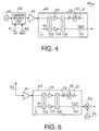
- FIG.4 is a block diagram showing a configuration of a transmission circuit of Embodiment 2 of the present invention.
- This transmission circuit comprises local oscillator 40, quadrature modulation circuit 43, pre-amplifier 44, balanced amplifier 45 explained in Embodiment 1 and antenna 46.
- Two signals that is, I signal and Q signal
- quadrature modulation circuit 43 via two signal input terminals 41 and 42.
- Balanced amplifier 45 can extract distortion signals without using any special distortion detection circuit. Balanced amplifier 45 is therefore suitable for miniaturization and low-cost implementation of a transmitter. Moreover, balanced amplifier 45 in FIG.4 has a feed-forward type configuration. That is, distortion of amplifier circuits 23 and 24 is fed back to circuits placed after amplifier circuits 23 and 24 to cancel out distortion. Thus, the amplified signal of the balanced amplifier is directly output to antenna 46, which is advantageous to achieving high efficiency and low distortion.
- FIG.5 is a circuit diagram showing a configuration of a reception circuit according to Embodiment 3 of the present invention.
- This reception circuit comprises antenna 50, low-noise amplifier 51, compensation circuit 52 using the balanced amplifier explained in Embodiment 1, down-converter 54 and local oscillator 53.
- the reception amplifier directly connected to antenna 50 is required to have low noise and low power consumption to amplify a high power signal received.
- the balanced amplifier of the present invention has a distortion compensation function, which improves an S/N ratio of an amplified signal. Furthermore, the present invention cancels out distortion using the characteristic of the balanced amplifier, which simplifies the configuration and is therefore suitable for miniaturization and low-cost implementation of a communication apparatus.
- balanced amplifier 52 is placed before down-converter 54, which allows the part with large reception power to amplify a normal reception signal. This has a merit of suppressing noise and easily improving the S/N ratio.
- the present invention uses one of ports of the power combiner as the one for detecting distortion generated in the amplifier circuit. This makes it possible to implement a small and high-performance balanced amplifier with a distortion compensation function.
- the present invention also requires no prior circuit adjustment for distortion detection.
Abstract
The present invention is a microwave power amplifier
using a balanced amplifier(22,23,24,25). The present
invention uses one output port(26b) of a hybrid power
combiner(25) as a port to detect distortion of the
amplifier circuit. To eliminate noise superimposed over
a normal signal, the detected distortion is fed back to
the normal amplified signal via an adjustment
circuit(28) and directional coupler(32).
Description
- The present invention relates to a power amplifier, and a microwave power amplifier with a non-linear distortion compensation function in particular.
- In line with development of increasingly smaller and lighter cellular telephones in recent years, an IC supply voltage has been reduced and increasingly lower power consumption is required. As an IC supply voltage decreases, transistors composing a power amplifier become saturated more easily. Thus, the amount of noise superimposed over an amplified output signal tends to increase.
- However, in order to meet stringent requirements from users, optimal communications using cellular telephones must be secured even in a low power consumption environment.
- In securing the communication quality, it is important to compensate non-linear distortion of a microwave power amplifier. An example of non-linear distortion compensation circuit of a power amplifier is described in the Japanese Patent Application No.HEI 6-37551.
- Suppressing non-linear distortion of the microwave power amplifier requires extraction of a distortion component signal in the first place. Then, the phase of the extracted distortion component signal is inverted. The inverted signal is superimposed over the original signal to cancel out the distortion component.
- However, separating only the distortion component from the output signal of the power amplifier requires a dedicated distortion extraction circuit, which will require more circuit parts. This may increase the cost of the apparatus.
- This also requires prior fine adjustment of added circuit parts. Such adjustment is troublesome.
- It is an objective of the present invention to reduce distortion of a microwave power amplifier while suppressing an increase in the number of parts of the circuit and avoiding trouble of prior adjustment of the circuit.
- The present invention uses a balanced amplifier comprising a hybrid power divider and hybrid power combiner for power amplification. The present invention actively uses one port (terminal) of the hybrid power combiner, which would normally be terminated, as a distortion detection port (terminal).
- That is, output ports other than the output ports for normal signals in the balanced amplifier circuit would conventionally be terminated with terminal resistors connected. However, these ports have the feature that a distortion component generated in the amplifier is outputted to these ports without being suppressed so much as a normal signal.
- Focusing on this finding, it is possible to extract distortion by using one port of the hybrid power combiner that would conventionally be terminated as a distortion detection port without using any special circuit. Adding desired adjustment to the output of this port and feeding this output back to the output of the power amplifier can cancel out the distortion component, thus eliminating the distortion component.
- It is desirable that the distortion signal outputted from one port of the hybrid power combiner be subjected to adjustment of attenuation of the signal level, phase shift or amplitude. This will enhance the distortion elimination effects.
- Mounting the power amplifier of the present invention in a mobile communication apparatus can secure a clear communication quality with less distortion.
- The above and other objects and features of the invention will appear more fully hereinafter from a consideration of the following description taken in connection with the accompanying drawing wherein one example is illustrated by way of example, in which;
- FIG.1 is a circuit diagram showing a configuration of a hybrid balanced power amplifier according to an embodiment of the present invention;
- FIG.2A is a diagram showing a frequency spectrum
of a signal in
signal transmission route 1 ○ of the power amplifier in FIG.1; - FIG.2B is a diagram showing a frequency spectrum
of a signal in
signal transmission route 2 ○ of the power amplifier in FIG.1; - FIG.2C is a diagram showing a frequency spectrum
of a signal in
signal transmission route 3 ○ of the power amplifier in FIG.1; - FIG.2D is a diagram showing a frequency spectrum
of a signal in
signal transmission route 4 ○ of the power amplifier in FIG.1; - FIG.3A is a diagram showing a general configuration of a hybrid balanced power amplifier;
- FIG.3B is a diagram showing an equivalent circuit of a general hybrid balanced amplifier;
- FIG.4 is a circuit diagram showing a configuration of a transmitter according to another embodiment of the present invention;
- FIG.5 is a circuit diagram showing a configuration of a receiver according to the other embodiment of the present invention;
- FIG.6 is a circuit diagram showing a configuration of a comparison example of hybrid balanced power amplifier;
- FIG.7A is a diagram sowing a frequency spectrum of
a signal in
signal transmission route 1 ○ of the hybrid balanced power amplifier in FIG.6; - FIG.7B is a diagram sowing a frequency spectrum of
a signal in
signal transmission route 2 ○ of the hybrid balanced power amplifier in FIG.6; - FIG.7C is a diagram sowing a frequency spectrum of
a signal in
signal transmission route 3 ○ of the hybrid balanced power amplifier in FIG.6; - FIG.7D is a diagram sowing a frequency spectrum of
a signal in
signal transmission route 4 ○ of the hybrid balanced power amplifier in FIG.6; and - FIG.8 is a characteristic diagram to explain non-linear distortion of a power amplifier circuit.
-
- With reference now to the attached drawings, the embodiments of the present invention are explained below.
- Before giving specific explanations of the embodiments, the configuration of a balanced amplifier and typical operation method (conventional operation method) are explained using FIG.3A and FIG.3B.
- FIG.3A is a diagram showing a basic configuration of the balanced amplifier and FIG.3B is an equivalent circuit diagram of the balanced amplifier.
- As shown in FIG.3B, the balanced amplifier divides a signal (IN) inputted to
input terminal 20a into two parts bypower divider 22 and amplifies the two divided signals by twoamplifier circuits output terminal 27b. - According to this configuration, the input signal is divided into two parts and the power of the signal is reduced to 1/2, and thus the load on each amplifier circuit (23, 24) is alleviated compared to the case of amplification using one amplifier.
- That is, transistors are less likely to become saturated, and thus it is easier to secure the linearity. Furthermore, since the amount of load on one amplifier circuit is reduced, this configuration has a merit of obtaining desired performance even using a low-priced circuit.
- More specifically, the balanced amplifier has a configuration as shown in FIG.3A. Both
power divider 22 and power combiner 25 have a hybrid configuration with 2 inputs and 2 outputs. - Here, a hybrid configuration refers to a configuration with 4 terminals (ports) used for the purpose of dividing an input signal into 2 signals or combining 2 signals into one signal.
- In FIG.3A, the input signal (IN) is inputted to one
input port 20a ofhybrid power divider 22. 50Ω terminal resistor R1 is connected toother input terminal 21a ofpower divider 22 to adjust impedance. - The signal (IN) inputted to
input port 20a is divided into two parts. The divided signals are outputted fromoutput ports - At this time, the phase of the signal outputted from
output port 20b via route "A" is the same as that of the input signal (IN), while the phase of the signal outputted fromoutput port 21b via route "B" is shifted by 90Q from the phase of the input signal (IN). - The signals outputted from
output ports power divider 22 are amplified byamplifier circuits input ports - Hybrid power combiner 25 combines the two signals inputted and outputs an amplified signal (normal signal OUT) from
output port 27b. 50Ω terminal resistor R2 is connected toother output port 26b. Thus, no normal signal is outputted from thisoutput port 26b. - That is, with
hybrid power combiner 25, a signal inputted to inputport 26a is divided into twooutput ports - Likewise, a signal inputted to input
port 27a is divided into twooutput ports - At this time, the phase of the signal outputted via route "C" and route "D" is shifted by 90º from the phase of the input signal. On the other hand, the phase of the signal outputted via route "E" and route "F" is the same phase as that of the input signal.
- Here, if attention is given to
output port 26b, the signal appearing at this port is a signal combining the signal coming via route "A" ofpower divider 22,amplifier circuit 23 and route "E" ofpower combiner 25 and the signal coming via route "B" ofpower divider 22,amplifier circuit 24 and route "D" ofpower combiner 25. - The signal coming via route "A" of
power divider 22 and the signal coming viaamplifier circuit 24 and route "D" ofpower combiner 25 are signals with the phase shifted by a total of 180º (= 90º+ 90º) with respect to the input signal (IN). On the other hand, the signal coming via route "E" ofpower combiner 25 is a signal with the same phase as that of the input signal (IN). - That is, since one signal and another signal with an 180Q phase shift with respect to the first one are added up, these two signals are canceled out and suppressed, and therefore no normal signal is outputted from
output port 26b. - On the other hand, if attention is given to
output port 27b ofpower combiner 25, the signal appearing at this port is a signal combining the signal coming via route "B" ofpower divider 22,amplifier circuit 24 and route "F" ofpower combiner 25 and the signal coming via route "A" ofpower divider 22,amplifier 23 and route "C" ofpower combiner 25. - Here, the signal coming via route "B" of
power divider 22,amplifier circuit 24 and route "F" ofpower combiner 25 is a signal with the phase shifted by 90Q with respect to the input signal (IN). On the other hand, the signal coming via route "A" ofpower divider 22,amplifier 23 and route "C" ofpower combiner 25 is likewise a signal with the phase shifted by 90º with respect to the input signal (IN). - That is, two signals with a 90º phase shift with respect to the input signal (IN) (that is, signals with the same phase) are added up. Therefore, an amplified normal signal (OUT) is outputted from
output port 27b. - This is the basic operation of the balanced amplifier.
- FIG.1 is a circuit diagram showing a configuration of a microwave power amplifier with a distortion compensation function of the present invention.
- As illustrated in the figure, the power amplifier of the present invention amplifies a microwave signal using a balanced amplifier with 2 inputs and 2 outputs. However, the balanced amplifier used has an operating mode different from that of the general one shown in FIG.3A.
- That is, the balanced amplifier shown in FIG.1 uses
output port 26b that would originally be terminated as a port to detect distortion generated inamplifier circuits adjustment circuit 28 is connected tooutput port 26b. -
Adjustment circuit 28 compriseslevel adjustment circuit 29,phase adjustment circuit 30 andamplifier circuit 31. The output ofadjustment circuit 28 is fed back to the normal signal obtained fromoutput port 27b viadirectional coupler 32. This eliminates distortion superimposed over the normal signal. - As shown above, the present embodiment is characterized by the use of
output port 26b (FIG.3A) ofpower combiner 25 that would conventionally be terminated as a distortion detection port ofamplifier circuits - This is further explained below:
- Non-linear distortion questioned here is generated in
amplifier circuits amplifier circuits - Consider here how signal distortion generated in
amplifier circuits output port 26b ofpower combiner 25. - Signal distortion (noise) generated in
amplifier circuit 23 reachesoutput port 26b viainput port 26a ofpower combiner 25 and route "E" without any phase shift. - On the other hand, distortion (noise) generated in
amplifier circuit 24 reachesoutput port 26b viainput port 27a ofpower combiner 25 and route "D" with a phase shift of 90º and is combined with the signal coming via route "E". The phase difference between these two signals is 90º. - As shown above, in the case of a normal signal (main signal), since two signals with a phase difference of 180º are combined by means of the function of the balanced circuit, the combined signal is strongly suppressed and not outputted from
output port 26b. - However, in the case of noise generated in
amplifier circuits output port 26b. - This means that in FIG.3A,
output port 26b ofpower combiner 25 that would conventionally be terminated has a function as the port for detecting distortion signals ofamplifiers - The present embodiment uses this new finding to simplify the configuration of the distortion detection circuit performing distortion detection without providing any special configuration and save time and trouble of prior adjustment for distortion detection.
- The configuration and operation of the distortion compensation circuit according to the present embodiment are explained below more specifically with reference to FIG.1.
- The balanced amplifier shown in the first stage in FIG.1 is the same as that explained in FIG.3A. The same components as those in FIG.3A are assigned the same reference symbols.
-
Adjustment circuit 28 comprisingvariable attenuator 29,phase shifter 30 andamplifier circuit 31 is connected tooutput port 26b ofpower combiner 25 that composes the balanced amplifier.Phase shifter 30 inverts the phase of a distortion signal. - This
adjustment circuit 28 is provided to adjust the level and phase of a distortion signal outputted fromoutput port 26b ofpower combiner 25, that is, the port for distortion detection. - The distortion signal whose amplitude and phase have been adjusted by
adjustment circuit 28 is added viadirectional coupler 32 to a normal signal outputted fromoutput port 27b ofpower combiner 25. At this time, the distortion signal to be added is a signal with a phase shifted by 180º from that of the normal signal (signal with an opposite phase). - In this way, the distortion signal superimposed over the normal signal is canceled out and distortion is eliminated.
- The operation above is explained using
frequency spectra 1 ○ to 4 ○ shown in FIG.2A to FIG.2D. -
Frequency spectrum 1 ○ shown in FIG.2A is the spectrum of the signal atinput terminal 20a in FIG.1. -
Frequency spectrum 2 ○ shown in FIG.2B is the spectrum of the signal atoutput terminal 27b in FIG.1. -
Frequency spectrum 3 ○ shown in FIG.2C is the spectrum of the signal at the output end ofadjustment circuit 28 in FIG.1. -
Frequency spectrum 4 ○ shown in FIG.2D is the spectrum of the signal at the output end ofoutput terminal 33 in FIG.1. - Here, suppose a case where two normal signals S1 and S2 with different frequencies are inputted to microwave power amplifier 6.
- When these input signals pass through the balanced amplifier, distortion components N1 and N2 are generated due to the non-linearity of
amplifier circuits amplifier circuits - On the other hand, distortion components N1 and N2 outputted from
output port 26b ofpower combiner 25 are subjected to processing such as attenuation, phase shift or amplification as required and their levels, etc. are adjusted (FIG.2C). - After the phases of these distortion signals N1 and N2 are inverted, N1 and N2 are added to the output signal (FIG.2B) of
port 27b ofpower combiner 25 viadirectional coupler 32. This results in normal signals S1 and S2 free of distortion as shown in FIG.2D. - The present embodiment uses
output terminal 26b of the balanced amplifier that conventionally would not be used as a distortion signal terminal, thus eliminating the need for a special circuit to extract distortion. Therefore, the present embodiment simplifies the configuration, and therefore is also suitable for a small-sized communication apparatus such as cellular telephone. - Since the present embodiment requires no special circuit, it is naturally not necessary to adjust the characteristic of such a circuit beforehand.
- FIG.6 shows a comparable circuit example (circuit described in the Japanese Patent Application No.HEI 6-37551) that does not use the present invention.
- In FIG.6, microwave power amplifier 6 actually consists of a plurality of balanced amplifiers made up of a hybrid power divider and hybrid power combiner.
- As characteristic b shown by the solid line in FIG.8, this microwave power amplifier 6 has an input/output characteristic that becomes saturated in a high input area and is likely to generate non-linear distortion. In FIG.8, characteristic a shown by the dotted line represents an ideal characteristic.
- Therefore, the circuit in FIG.6 is provided with
directional couplers first adjustment circuit 2 that adjusts the signal level and phase andsecond adjustment circuit 9 that adjusts the level and phase, etc. of the extracted distortion signal. - The output of
second adjustment circuit 9 is fed back to the output signal of power amplifier 6 viadirectional coupler 13, thereby eliminating non-linear distortion of power amplifier 6. - Frequency spectra of signals in
different parts 1 ○ to 4 ○ in FIG.6 are shown in FIG.7A to FIG.7D, respectively. - The circuit of the present invention shown in FIG.1 does not require a special circuit to detect distortion signals such as the conventional circuit in FIG.6. That is, the circuit of the present invention does not require
directional couplers adjustment circuit 2. Therefore, the present invention has a simple configuration and is also suitable for miniaturization of a communication apparatus such as cellular telephone. - The present invention also effectively and reliably detects noise using the intrinsic characteristic of a balanced amplifier that noise generated in an amplifier circuit is suppressed by the balanced amplifier not so effectively as a normal signal. Therefore, the present invention does not require prior adjustment of the characteristic by
adjustment circuit 2 as in the case of the conventional circuit in FIG.6, thus simplifying adjustment of the circuit. - FIG.4 is a block diagram showing a configuration of a transmission circuit of
Embodiment 2 of the present invention. - This transmission circuit comprises
local oscillator 40,quadrature modulation circuit 43,pre-amplifier 44,balanced amplifier 45 explained inEmbodiment 1 andantenna 46. Two signals (that is, I signal and Q signal) with a phase difference of 90º are inputted toquadrature modulation circuit 43 via twosignal input terminals -
Balanced amplifier 45 can extract distortion signals without using any special distortion detection circuit.Balanced amplifier 45 is therefore suitable for miniaturization and low-cost implementation of a transmitter. Moreover,balanced amplifier 45 in FIG.4 has a feed-forward type configuration. That is, distortion ofamplifier circuits amplifier circuits antenna 46, which is advantageous to achieving high efficiency and low distortion. - FIG.5 is a circuit diagram showing a configuration of a reception circuit according to
Embodiment 3 of the present invention. - This reception circuit comprises
antenna 50, low-noise amplifier 51,compensation circuit 52 using the balanced amplifier explained inEmbodiment 1, down-converter 54 andlocal oscillator 53. - The reception amplifier directly connected to
antenna 50 is required to have low noise and low power consumption to amplify a high power signal received. However, these are characteristics basically contradictory to each other and it is quite difficult to implement both low noise and low power consumption under severe low cost and miniaturization requirements. - However the balanced amplifier of the present invention has a distortion compensation function, which improves an S/N ratio of an amplified signal. Furthermore, the present invention cancels out distortion using the characteristic of the balanced amplifier, which simplifies the configuration and is therefore suitable for miniaturization and low-cost implementation of a communication apparatus.
- Moreover, as shown in FIG.5,
balanced amplifier 52 is placed before down-converter 54, which allows the part with large reception power to amplify a normal reception signal. This has a merit of suppressing noise and easily improving the S/N ratio. - As explained above, the present invention uses one of ports of the power combiner as the one for detecting distortion generated in the amplifier circuit. This makes it possible to implement a small and high-performance balanced amplifier with a distortion compensation function. The present invention also requires no prior circuit adjustment for distortion detection.
- The present invention is not limited to the above described embodiments, and various variations and modifications may be possible without departing from the scope of the present invention.
- This application is based on the Japanese Patent Application No.HEI10-234581 filed on August 20, 1998, entire content of which is expressly incorporated by reference herein.
Claims (5)
- A power amplifier circuit equipped with a compensation circuit comprising:a hybrid power divider(22);a hybrid power combiner(25);at least one amplifiers provided between said hybrid power divider and hybrid power combiner(23,24);an adjustment circuit(28) that carries out predetermined processing on a distortion signal outputted from an output port(26b) other than the output port(27b) of a normal signal of said hybrid power combiner(25); anda feedback circuit(32) that feeds back the output of said adjustment circuit to the normal signal outputted from the output port(27b) of said normal signal of said hybrid power combiner.
- The power amplifier circuit according to claim 1, wherein said adjustment circuit further comprises a variable attenuator(29), phase shifter(30) and amplifier circuit(31).
- The power amplifier circuit according to claim 1, wherein said hybrid power divider(22) further comprises a first input port(20a) to which an input signal is supplied, second input port(21a) to which a terminal resistor is connected and first and second output ports(20b,21b),said hybrid power combiner(25) further comprises first and second input ports(26a,27a), a first output port(26b) that functions as a distortion detection port and a second output port(27b) that functions as an output port of a normal signal,a first amplifier circuit(23) is connected between said first output port(20b) of said hybrid power divider(22) and said first input port(26a) of said hybrid power combiner(25), anda second amplifier circuit(24) is connected between said second output port(21b) of said hybrid power divider(22) and said second input port(27a) of said hybrid power combiner(25).
- A transmitter comprising the power amplifier circuit according to claim 1.
- A receiver comprising the power amplifier circuit according to claim 1.
Priority Applications (3)
| Application Number | Priority Date | Filing Date | Title |
|---|---|---|---|
| US09/494,541 US6239656B1 (en) | 2000-01-31 | 2000-01-31 | Power amplifier |
| CA002298317A CA2298317C (en) | 2000-01-31 | 2000-02-10 | Microwave power amplifier |
| EP00103152A EP1126595A1 (en) | 2000-01-31 | 2000-02-16 | Power amplifier |
Applications Claiming Priority (3)
| Application Number | Priority Date | Filing Date | Title |
|---|---|---|---|
| US09/494,541 US6239656B1 (en) | 2000-01-31 | 2000-01-31 | Power amplifier |
| CA002298317A CA2298317C (en) | 2000-01-31 | 2000-02-10 | Microwave power amplifier |
| EP00103152A EP1126595A1 (en) | 2000-01-31 | 2000-02-16 | Power amplifier |
Publications (1)
| Publication Number | Publication Date |
|---|---|
| EP1126595A1 true EP1126595A1 (en) | 2001-08-22 |
Family
ID=27171162
Family Applications (1)
| Application Number | Title | Priority Date | Filing Date |
|---|---|---|---|
| EP00103152A Withdrawn EP1126595A1 (en) | 2000-01-31 | 2000-02-16 | Power amplifier |
Country Status (3)
| Country | Link |
|---|---|
| US (1) | US6239656B1 (en) |
| EP (1) | EP1126595A1 (en) |
| CA (1) | CA2298317C (en) |
Families Citing this family (4)
| Publication number | Priority date | Publication date | Assignee | Title |
|---|---|---|---|---|
| KR100406872B1 (en) * | 2001-09-11 | 2003-11-21 | 미션텔레콤 주식회사 | A postdistortion linearizer using diode mixer for improving intermodulation distortion of power amplifier |
| JPWO2004051790A1 (en) * | 2002-11-15 | 2006-04-06 | パナソニック モバイルコミュニケーションズ株式会社 | Active antenna |
| US7339426B2 (en) * | 2004-03-19 | 2008-03-04 | Powerwave Technologies, Inc. | High efficiency linear amplifier employing dynamically controlled back off |
| US7440733B2 (en) * | 2004-04-09 | 2008-10-21 | Powerwave Technologies, Inc. | Constant gain nonlinear envelope tracking high efficiency linear amplifier |
Citations (4)
| Publication number | Priority date | Publication date | Assignee | Title |
|---|---|---|---|---|
| US4564816A (en) * | 1984-05-09 | 1986-01-14 | Rca Corporation | Predistortion circuit |
| US4656434A (en) * | 1986-02-03 | 1987-04-07 | Raytheon Company | RF power amplifier with load mismatch compensation |
| JPH04301905A (en) * | 1991-03-28 | 1992-10-26 | Mitsubishi Electric Corp | Distortion generating circuit |
| EP0936731A1 (en) * | 1998-02-09 | 1999-08-18 | Matsushita Electric Industrial Co., Ltd. | Feed forward amplifier |
Family Cites Families (5)
| Publication number | Priority date | Publication date | Assignee | Title |
|---|---|---|---|---|
| FR2482799A1 (en) * | 1980-05-14 | 1981-11-20 | Lgt Lab Gen Telecomm | DEVICE FOR PRECORRECTION OF NON-LINEARITY PRODUCTS AND TELEVISION SIGNAL TRANSMISSION SYSTEM COMPRISING SUCH A DEVICE |
| US4439740A (en) * | 1982-04-01 | 1984-03-27 | Rockwell International Corporation | Corporate amplifier apparatus with improved degradation |
| US5287069A (en) * | 1990-02-07 | 1994-02-15 | Fujitsu Limited | Constant-amplitude wave combination type amplifier |
| JPH0637551A (en) | 1992-07-17 | 1994-02-10 | Fujitsu Ltd | Distortion compensation circuit |
| US6128479A (en) * | 1998-06-04 | 2000-10-03 | Motorola, Inc. | Radio frequency amplifier structure |
-
2000
- 2000-01-31 US US09/494,541 patent/US6239656B1/en not_active Expired - Fee Related
- 2000-02-10 CA CA002298317A patent/CA2298317C/en not_active Expired - Fee Related
- 2000-02-16 EP EP00103152A patent/EP1126595A1/en not_active Withdrawn
Patent Citations (4)
| Publication number | Priority date | Publication date | Assignee | Title |
|---|---|---|---|---|
| US4564816A (en) * | 1984-05-09 | 1986-01-14 | Rca Corporation | Predistortion circuit |
| US4656434A (en) * | 1986-02-03 | 1987-04-07 | Raytheon Company | RF power amplifier with load mismatch compensation |
| JPH04301905A (en) * | 1991-03-28 | 1992-10-26 | Mitsubishi Electric Corp | Distortion generating circuit |
| EP0936731A1 (en) * | 1998-02-09 | 1999-08-18 | Matsushita Electric Industrial Co., Ltd. | Feed forward amplifier |
Non-Patent Citations (1)
| Title |
|---|
| RODRIGO CORDEIRO TUPYNAMBA ET AL: "MESFET NONLINEARITIES APPLIED TO PREDISTORTION LINEARIZER DESIGN", INTERNATIONAL MICROWAVE SYMPOSIUM DIGEST (MTT-S),US,NEW YORK, IEEE, vol. -, 1992, pages 955 - 958, XP000343462 * |
Also Published As
| Publication number | Publication date |
|---|---|
| CA2298317C (en) | 2002-07-30 |
| US6239656B1 (en) | 2001-05-29 |
| CA2298317A1 (en) | 2001-08-10 |
Similar Documents
| Publication | Publication Date | Title |
|---|---|---|
| US7725082B2 (en) | Radio communication apparatus, radio communication method, antenna apparatus and first duplexer | |
| US20060128322A1 (en) | Transceiver apparatus and module | |
| EP1710920A1 (en) | Receiving modulated radio signals | |
| US7003263B2 (en) | Telecommunications receiver and a transmitter | |
| US20010015673A1 (en) | Feed-forward amplifier and controller of the same | |
| US7555280B2 (en) | Apparatus for frequency direct conversion reception in mobile communication terminal and method thereof | |
| KR20070000257A (en) | Doherty amplifier and transmitter using mixer | |
| KR20060136227A (en) | Doherty Amplifier and Transmitter Using Mixer | |
| US6236848B1 (en) | Receiver integrated circuit for mobile telephone | |
| EP3278459B1 (en) | Receiving a plurality of radio frequency bands | |
| US7747227B2 (en) | Transmission module | |
| US10944438B2 (en) | Communication unit | |
| US6393011B1 (en) | Receiving circuit of mobile communication terminal having feed forward linearizer | |
| JP2005124175A (en) | Amplifier and frequency converter | |
| CA2298317C (en) | Microwave power amplifier | |
| US7209715B2 (en) | Power amplifying method, power amplifier, and communication apparatus | |
| US6850752B2 (en) | Single-to-differential conversion circuit outputting DC-balanced differential signal | |
| US6128478A (en) | Apparatus and method for amplifying a radio frequency signal | |
| US7636562B1 (en) | Radio frequency mixer and method of operation | |
| US6292055B1 (en) | Electronic apparatus comprising a power amplifier | |
| EP1022848B1 (en) | Amplifier and radio communication apparatus using the same | |
| US20050136847A1 (en) | Communication semiconductor integrated circuit device and electrical apparatus | |
| US9071317B2 (en) | Nullification of transmitter noise at receive signal frequency | |
| JP2000068754A (en) | Distortion compensating circuit | |
| KR100380723B1 (en) | Digital satellite receiver with capability of improving receiving sensitivity in low field area |
Legal Events
| Date | Code | Title | Description |
|---|---|---|---|
| PUAI | Public reference made under article 153(3) epc to a published international application that has entered the european phase |
Free format text: ORIGINAL CODE: 0009012 |
|
| AK | Designated contracting states |
Kind code of ref document: A1 Designated state(s): AT BE CH CY DE DK ES FI FR GB GR IE IT LI LU MC NL PT SE |
|
| AX | Request for extension of the european patent |
Free format text: AL;LT;LV;MK;RO;SI |
|
| 17P | Request for examination filed |
Effective date: 20011008 |
|
| AKX | Designation fees paid |
Free format text: DE FR GB NL |
|
| STAA | Information on the status of an ep patent application or granted ep patent |
Free format text: STATUS: THE APPLICATION HAS BEEN WITHDRAWN |
|
| 18W | Application withdrawn |
Effective date: 20050202 |