EP1079259B1 - Manufacturing method of a display module comprising a liquid crystal cell - Google Patents
Manufacturing method of a display module comprising a liquid crystal cell Download PDFInfo
- Publication number
- EP1079259B1 EP1079259B1 EP99116938.4A EP99116938A EP1079259B1 EP 1079259 B1 EP1079259 B1 EP 1079259B1 EP 99116938 A EP99116938 A EP 99116938A EP 1079259 B1 EP1079259 B1 EP 1079259B1
- Authority
- EP
- European Patent Office
- Prior art keywords
- cell
- printed circuit
- module
- display
- pads
- Prior art date
- Legal status (The legal status is an assumption and is not a legal conclusion. Google has not performed a legal analysis and makes no representation as to the accuracy of the status listed.)
- Expired - Lifetime
Links
Images


Classifications
-
- H—ELECTRICITY
- H05—ELECTRIC TECHNIQUES NOT OTHERWISE PROVIDED FOR
- H05K—PRINTED CIRCUITS; CASINGS OR CONSTRUCTIONAL DETAILS OF ELECTRIC APPARATUS; MANUFACTURE OF ASSEMBLAGES OF ELECTRICAL COMPONENTS
- H05K1/00—Printed circuits
- H05K1/18—Printed circuits structurally associated with non-printed electric components
- H05K1/189—Printed circuits structurally associated with non-printed electric components characterised by the use of a flexible or folded printed circuit
-
- G—PHYSICS
- G02—OPTICS
- G02F—OPTICAL DEVICES OR ARRANGEMENTS FOR THE CONTROL OF LIGHT BY MODIFICATION OF THE OPTICAL PROPERTIES OF THE MEDIA OF THE ELEMENTS INVOLVED THEREIN; NON-LINEAR OPTICS; FREQUENCY-CHANGING OF LIGHT; OPTICAL LOGIC ELEMENTS; OPTICAL ANALOGUE/DIGITAL CONVERTERS
- G02F1/00—Devices or arrangements for the control of the intensity, colour, phase, polarisation or direction of light arriving from an independent light source, e.g. switching, gating or modulating; Non-linear optics
- G02F1/01—Devices or arrangements for the control of the intensity, colour, phase, polarisation or direction of light arriving from an independent light source, e.g. switching, gating or modulating; Non-linear optics for the control of the intensity, phase, polarisation or colour
- G02F1/13—Devices or arrangements for the control of the intensity, colour, phase, polarisation or direction of light arriving from an independent light source, e.g. switching, gating or modulating; Non-linear optics for the control of the intensity, phase, polarisation or colour based on liquid crystals, e.g. single liquid crystal display cells
- G02F1/133—Constructional arrangements; Operation of liquid crystal cells; Circuit arrangements
- G02F1/1333—Constructional arrangements; Manufacturing methods
- G02F1/133308—Support structures for LCD panels, e.g. frames or bezels
-
- G—PHYSICS
- G02—OPTICS
- G02F—OPTICAL DEVICES OR ARRANGEMENTS FOR THE CONTROL OF LIGHT BY MODIFICATION OF THE OPTICAL PROPERTIES OF THE MEDIA OF THE ELEMENTS INVOLVED THEREIN; NON-LINEAR OPTICS; FREQUENCY-CHANGING OF LIGHT; OPTICAL LOGIC ELEMENTS; OPTICAL ANALOGUE/DIGITAL CONVERTERS
- G02F1/00—Devices or arrangements for the control of the intensity, colour, phase, polarisation or direction of light arriving from an independent light source, e.g. switching, gating or modulating; Non-linear optics
- G02F1/01—Devices or arrangements for the control of the intensity, colour, phase, polarisation or direction of light arriving from an independent light source, e.g. switching, gating or modulating; Non-linear optics for the control of the intensity, phase, polarisation or colour
- G02F1/13—Devices or arrangements for the control of the intensity, colour, phase, polarisation or direction of light arriving from an independent light source, e.g. switching, gating or modulating; Non-linear optics for the control of the intensity, phase, polarisation or colour based on liquid crystals, e.g. single liquid crystal display cells
- G02F1/133—Constructional arrangements; Operation of liquid crystal cells; Circuit arrangements
- G02F1/1333—Constructional arrangements; Manufacturing methods
- G02F1/1345—Conductors connecting electrodes to cell terminals
- G02F1/13452—Conductors connecting driver circuitry and terminals of panels
-
- G—PHYSICS
- G04—HOROLOGY
- G04G—ELECTRONIC TIME-PIECES
- G04G17/00—Structural details; Housings
- G04G17/02—Component assemblies
-
- G—PHYSICS
- G02—OPTICS
- G02F—OPTICAL DEVICES OR ARRANGEMENTS FOR THE CONTROL OF LIGHT BY MODIFICATION OF THE OPTICAL PROPERTIES OF THE MEDIA OF THE ELEMENTS INVOLVED THEREIN; NON-LINEAR OPTICS; FREQUENCY-CHANGING OF LIGHT; OPTICAL LOGIC ELEMENTS; OPTICAL ANALOGUE/DIGITAL CONVERTERS
- G02F1/00—Devices or arrangements for the control of the intensity, colour, phase, polarisation or direction of light arriving from an independent light source, e.g. switching, gating or modulating; Non-linear optics
- G02F1/01—Devices or arrangements for the control of the intensity, colour, phase, polarisation or direction of light arriving from an independent light source, e.g. switching, gating or modulating; Non-linear optics for the control of the intensity, phase, polarisation or colour
- G02F1/13—Devices or arrangements for the control of the intensity, colour, phase, polarisation or direction of light arriving from an independent light source, e.g. switching, gating or modulating; Non-linear optics for the control of the intensity, phase, polarisation or colour based on liquid crystals, e.g. single liquid crystal display cells
- G02F1/133—Constructional arrangements; Operation of liquid crystal cells; Circuit arrangements
- G02F1/1333—Constructional arrangements; Manufacturing methods
- G02F1/133308—Support structures for LCD panels, e.g. frames or bezels
- G02F1/133322—Mechanical guidance or alignment of LCD panel support components
Definitions
- the invention relates to a method for producing a display module comprising at least one liquid crystal cell connected to a display control printed circuit whose electronic components for the control of the cell and the connection metal tracks. said components and said cell are arranged on one side.
- the invention also relates to a display module that can be obtained according to the method, as well as a watch comprising a display module.
- liquid crystal cell displays are used, for example for calculators or for various information display devices, which are linked to one or more printed circuits with electronic components for the control of the electrodes. of the cell.
- some electronic control components of the cell are placed on the blade of the cell also bearing the conductive pads connected to the electrodes.
- the surface defined by the cell connected to the display control circuit board (s) next to the cell is often too large to be placed in a box of a small device where it is necessary. to have compact display modules.
- the printed circuit boards for said cells are usually rigid and most often their metallic output pads are electrically connected to the respective conductive pads of the liquid crystal cell by connection strips called "zebra" interposed between said pads.
- the contact pressure required for this type of connection induces a certain mechanical tension between the cell, its support and the printed circuit, which can be a disadvantage.
- the location of the printed circuit board, whether it is below or adjacent to the liquid crystal cell to be connected, is generally not very important. Only in modular embodiments where the printed circuit is usually placed below the cell with in this case said connection strips being part of spacer elements.
- the display module includes a frame of the module for enclosing a liquid crystal cell, a spacer element and a rigid printed circuit comprising all the electronic control components of said cell.
- the printed circuit board may be single-sided on which a connection strip forming part of the spacer element is compressed in the frame to connect on one side metal output strips of the printed circuit and on the other side of the connected conductive pads to the electrodes of the liquid crystal cell.
- the display module is mechanically and electrically connected to a flexible printed circuit for, in particular, supplying power to said module.
- the electrical connection between this flexible printed circuit and the module is at the surface of the rigid printed circuit bearing metal tracks output module. There is no use of glue for maintaining the electrical connection, but the end of the flexible circuit is pressed between the spacer and the output metal tracks disposed on the rigid printed circuit.
- said flexible printed circuit comprises two openings which fit on two pillars of the rigid printed circuit to allow particular precise positioning for the electrical connection. It can be seen that the frame serves to mount all the elements of said module, as well as to connect the flexible printed circuit to said module.
- This display device comprises a liquid crystal cell and a printed circuit bearing on a single side at least one integrated control circuit of the cell.
- the face without components of the printed circuit is arranged opposite the back of the cell.
- An end portion of the printed circuit is folded at 180 ° and attached to a silicon gap member.
- the end of the circuit board fixed on the space element carries a series of metal tracks connecting the integrated circuit.
- the metal tracks are connected to corresponding ranges of the liquid crystal cell by a thermo-compression operation with the interposition of a conductive adhesive.
- the display device thus designed does not include any means to properly position the display of the cell during mounting in a box of a device, which is a drawback.
- the present invention aims to obviate the disadvantages of the display modules described above. It proposes to make a compact display module and thin, arranged so that you can easily and accurately mount this module in a box of a device so that the display is in a specific position. Said module can be mounted in particular in a box of a wristwatch.
- a solution for producing said module consists in placing the printed circuit on the side of the back of the cell, in positioning it so that means for assembling the module made on the printed circuit define, with respect to means for locating the display. arranged on the cell, the location of the display of the cell, and to fix the face without components of the printed circuit at the back of the cell according to the characterizing part of claim 1.
- Another solution for producing said module is to place the printed circuit on the back side of the cell, to fix the non-component side of the printed circuit on the back of the cell, and to make assembly means of the module on the printed circuit. positioned relative to display locating means disposed on the cell to define the location of the display of the cell according to the characterizing part of claim 2.
- the thickness of the cell with the single-sided printed circuit, whose face without components is fixed directly to the back of said cell to make it compact, is reduced at least so that it can be mounted, for example, in a digital watch thin. It is clear that this thickness is largely dependent on that of the said cell that is a component obtained on the market and whose thickness is around 1 mm. It is possible in the near future to obtain such cells with a thickness of less than 1 mm.
- Another advantage of the module that is the subject of the invention is that, since the printed circuit has all the electronic components and the metal tracks on a single surface of said printed circuit, the manufacturing costs are minimized by avoiding the creation of holes. metallized through the printed circuit to establish an electrical connection of metal tracks and components that would be arranged on both sides. The assembly of electronic components on the printed circuit is also facilitated. In addition, the arrangement of the metal tracks is made so that said tracks do not cross over the entire printed circuit. It is therefore necessary that the output terminals of the integrated control circuit of the cell are in agreement with the respective terminals to contact the cell so that the metal tracks from the output terminals of the integrated circuit do not cross until the connection. to the cell.
- the spacing that is to say the pitch which is the width plus a track and a space, can be less than 0.5 mm, and even less than 0.3 mm, but it depends on what is currently supplied in the market as liquid crystal cells. With this reduced spacing, it is possible to precisely position the tongue of the printed circuit bearing the metal connection pads to the cell above the respective conductive pads of the cell and to connect said pads electrically with the aid of an anisotropic conductive adhesive which only becomes conductive when compressed and applied with heat.
- the following description relates to the realization of a display module for a digital wristwatch, but the use of such a module is of course not limited to watchmaking; it could also be used in other areas where it is necessary to make said compact module, thin and easy to mount precisely in a box of a device through assembly means on the printed circuit, while ensuring a good positioning of the display.
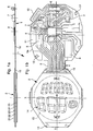
- the display module comprises a flexible printed circuit 1 having a polyimide or polyester substrate 1a of thickness less than or equal to 150 ⁇ m, preferably 75 ⁇ m, and at least one liquid crystal cell 2.
- the flexible printed circuit 1 comprises on one side metal tracks 5 connecting the liquid crystal cell 2 and the electronic components, namely a quartz resonator 6, resistors and capacitors 7 and an integrated control circuit of the display 8 At one end, it comprises a tongue 3 carrying metal pads 4 for connection to the liquid crystal cell 2. These metal strips 4 are regularly spaced or not and placed in parallel next to each other depending on the conductive pads arranged in the same manner with an equivalent spacing under an extension 16 of the first blade 22 of the liquid crystal cell 2.
- a metal terminal 9 is provided for the supply contact from the negative pole of a battery.
- a metal terminal 11 allows the contact of a plate of connection of the plate the bottom of the watch case, this plate being connected to the positive pole of the battery.
- a metal terminal 10 which can be folded and glued against an edge of the cell to serve in contact with a control blade 43 actuated by a push button 42, visible in Figures 4a and 4b , in order to display on the cell the various time and date information, as well as for setting the times and dates. It should be noted that it is not essential to fold this portion of the printed circuit bearing the terminal 10, because the blade 43 could very well slide under the printed circuit and contact the terminal 10 from below.
- the integrated circuit 8 is made so that the metal tracks 5 connecting the outputs of the integrated circuit 8 with the conductive pads to be connected and the discrete components 6 and 7 mounted on the printed circuit 2 do not cross.
- the printed circuit also comprises means for assembling the module positioned in relation to the targets 13 of the cell, whether optically or mechanically by using the assembly means for moving the printed circuit. This positioning of the printed circuit relative to the cell can of course also be operated with other tracking means or other targets placed on said circuit visible for example by transparency. In this case, the targets or the marking means are optically aligned in a perfectly precise manner.
- the final assembly means are two holes 12 arranged on two ears 17 placed at the ends of a diagonal of the printed circuit. Once the module is finished, the two holes 12 make it possible to mount the module precisely laterally on two nubs 41 of the watch case, visible in Figures 4a and 4b in order to have a display of the cell in a perfectly determined and precise position.
- the shape of the holes 12 is not necessarily circular. One can provide a hole of oval shape and the other of circular shape.
- the liquid crystal cell 2 which may be of the nematic type (TN), comprises a polarizing film 21 fixed on the first blade 22.
- the second blade 23 is fixed under the first blade 22.
- the two blades are configured to enclose the liquid crystals together.
- a last polarizer / reflector plate 24 is fixed under the second plate 23 to allow the polarization and reflection of the incoming light from the polarizer film 21 on the display side 14.
- the thickness of such a cell is less than 1.1 mm, each blade being less than or equal to 0.3 mm thick and the polarizing film being less than 0.2 mm thick.
- the shape of the cell is, for example, octagonal so that it can be mounted in a circular wristwatch box with a visible part of the outside having a diameter of around 20 mm, shown in broken lines on the Figures 1 to 3 , under the watch glass, but it is clear that the shape of the cell could also be rectangular to be mounted in a rectangular box.
- the flexible printed circuit 1 is provided, according to common techniques, a coil, not shown in the figures, on which is wound a strip comprising several printed circuits arranged one after the other on said strip, of which only the tracks 5 metal, especially copper, on one side are made. It is important to design everything on one side, because we avoid the need to make metallized holes to create electrical connection passages from one side to another, as a measure of economy and ease of assembly of electronic components .
- one or more printed circuit boards 1 are placed in position in order to be able to mount the electronic components 6, 7 and 8 on each single-face printed circuit board before or after having cut from the strip the series of identical printed circuits.
- the tabs 3 of the printed circuits 1 can be arranged perpendicular to the longitudinal axis of the strip, that is to say with respect to one of the edges of the strip. This assembly can be automated as is customary to the knowledge of a person skilled in this field.
- the metal strips 4 of the tongue 3 of the printed circuit are connected to the corresponding ranges of the liquid crystal cell 2.
- the face of the circuit board 1 without components is first held on a flat surface for this process step.
- An anisotropic conductive adhesive strip is placed either at the ends of the metal pads 4 of the printed circuit, or on the conductive pads of the cell 2 before this connection.
- the extension 16 of the first blade 22 of the cell 2 carrying the conductive pads is brought above the metal pads 4 at the end of the tongue 3 with interposition of the anisotropic adhesive strip, the metal and conductive pads facing each other. .
- Targets 13, numbering four, provided in FIG. as reference means on the blade 22, can also be used for the camera to position said tab, but given the transparency of the edge of the first blade 22 of the cell and the vision of the conductive pads under the glass, the targets 13 do not are not considered necessary at this process step.
- the extension 16 of the blade 22 is pressed against the tongue 3 by heating for bonding, for example at a temperature of around 180 ° C.
- Said anisotropic adhesive consists of a thermosetting resin with incorporated conductive powder. She becomes a conductor only when she is compressed. Since the metal and conductive pads are protruding portions on the printed circuit and the extension with gaps between each range, the adhesive is compressed only between each metal pad 4 connected to the respective conductive pad of the cell. 2. On the other hand, in the empty spaces between the conductive areas and the empty spaces between the metal areas, the glue will remain insulating. The connection of each metal pad with each conductive pad is over a distance of 1 mm to 2 mm.
- the center-to-center spacing of the metal pads on the tongue 3 is equivalent to the spacing of the conductive pads to be connected from the cell 2. Previously with the use of terminal strips, the spacing was about 0.5 mm. With this connection without said strips, it is possible to reduce this spacing below 0.3 mm without creating a short circuit between said ranges.
- the width of a metal strip is of the order of 0.15 mm and the space separating two neighboring ranges is of the order of 0.15 mm. Spaces and beaches are not necessarily equal in size.
- an artificial vision device 50 is used for the positioning of the printed circuit relative to the cell.
- An image of the cell 2 with these targets 13, defining the location of the display 14 ( figure 1b ), is stored before folding the circuit board above the cell.
- the cell 2 on the display side is held on a flat surface in a pose.
- the flexible printed circuit 1 held by a suction tool, is folded so as to be parallel to a position spaced above the back of the cell, the face without components being opposite the back of said cell.
- the area of the printed circuit is slightly larger than that of the cell, so that when positioning X and Y, it covers almost completely said cell.
- the printed circuit comprising two holes 12 as assembly means of the module, is moved along the X and Y axes parallel to the back of the cell so as to position it relative to the stored targets 13 defining the location of the display 14 of the liquid crystal cell 2.
- the assembly means of the module which are the two holes 12 made on two ears 17, or the stored image. of the printed circuit, knowing that according to this image the position of the holes 12 is well defined with respect to the location of the display of the cell.
- a displacement according to Y may be sufficient in this process step if the X positioning has already been made in the step of connecting the tongue 3 under the extension 16 of the first blade 22 of the cell 2.
- the holes 12 of the printed circuit 1 can be made at the end of the manufacturing process of said module instead of being already present initially.
- the non-component side of the flexible printed circuit is bonded under the cell, leaving two ear-shaped parts 17 of the printed circuit accessible after bonding. Then, a tool comes to drill each of the two holes 12 on the ears 17 according to the location of the display 14 with the help of the targets 13 stored by the artificial vision device 50.
- the tongue can be made with a central opening , the metal tracks 5 ending in the metal connection pads 4 to pass around the opening.
- An anisotropic conductive adhesive strip is placed either on the end of the metal strips of the tongue 3 or on the conductive pads of the cell.
- the opening of the tongue is provided so that one can with a tool press and heat the tongue 3 once positioned for its electrical and mechanical connection to the conductive pads of the cell under said extension 16.
- the locating means used for the positioning of the printed circuit 1 with the cell 2 could consist, instead of the targets 13, of the display itself if the cell was supplied with electricity.
- the printed circuit 1 comprises two tongues 3 arranged next to each other each carrying the metal pads 4 of connection to the conductive pads of the corresponding cell.
- a band of glue is placed either on the extensions 16 of each of the cells or on the tongues 3. As soon as the tongues 3 are positioned on the conductive pads of each of the cells, they are pressed and heated for their fixation, as explained more high.
- the printed circuit at the tabs is bent at 180 ° so as to lie parallel to a distance from the back of the second cell, and positioned in X and Y, before being moved according to the Z axis to stick on a double-sided sticky tape 25 placed under the second cell.
- the tongue 3 connecting the first cell describes a greater radius of curvature than the tongue 3 connecting the second cell.
- the fixing of the tongues 3 under the extensions 16 of the first blades 22 of the cells can be performed after having positioned and fixed the face without components of the printed circuits on the back of the second cell.
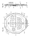
- FIGs 4a and 4b it is represented the mounting of the display module 30 in a watch case 40.
- the two holes 12 made on the printed circuit can maintain and position said module 30 in its own plane easily and precisely in said box 40 on two nipples 41, came from molding with the plastic box.
- the module once placed on the two nipples makes it possible to have a display positioned laterally in the watch case with an accuracy of less than 100 ⁇ m.
- the module 30 is sealed to the box by deforming, by heating, or by ultrasound or other means of deformation, the summit portion of the nipples 41.
- the liquid crystal cell can rest on four supports of the box once the module is placed on the nipples 41. But it can also be expected to fix said module on the bottom of the box without the use of supports of the cell, in order to gain even on the thickness of the watch of the order of 3.9 mm. It should be known that the thickness of the module, of the order of 2.7 mm, is dependent on the thickness of the cell 2 and also that of the quartz resonator 6 and the discrete components 7.
- the figure 5 shows only a part of the flexible printed circuit which is folded and glued against an edge of the cell, said portion carrying a metal terminal 10 for the contact of a flexible conductive control lamella 43 pushed by a pushbutton 42, visible to Figures 4a and 4b .
- a pushbutton 42 By pressing the pushbutton 42, one can select different display modes of the cell, and set the hours and dates of the watch.
- the figure 6 shows a vertical section of the completed assembly of the watch with its display module 30.
- the lens 44 of the watch includes an opaque peripheral ring 45 to hide the edges of the cell and the elements of the bottom of the box 40, so that remains visible that part 15 ( figure 1b ) of the display.
- the box is molded in plastic with a bottom metal plate 46 connected to the positive pole of the battery.
- the invention that has just been described is not limited, of course, to the realization of the display module of a wristwatch, but covers any display module, within the reach of a person skilled in the art, having assembly means, made on the printed circuit fixed to the back of the cell and positioned relative to the location of the display, to facilitate mounting on complementary means made in a device receiving it.
Landscapes
- Physics & Mathematics (AREA)
- Nonlinear Science (AREA)
- General Physics & Mathematics (AREA)
- Mathematical Physics (AREA)
- Chemical & Material Sciences (AREA)
- Crystallography & Structural Chemistry (AREA)
- Optics & Photonics (AREA)
- Engineering & Computer Science (AREA)
- Microelectronics & Electronic Packaging (AREA)
- Electric Clocks (AREA)
- Devices For Indicating Variable Information By Combining Individual Elements (AREA)
Description
L'invention concerne un procédé de réalisation d'un module d'affichage comprenant au moins une cellule à cristaux liquides reliée à un circuit imprimé de commande de l'affichage dont les composants électroniques pour la commande de la cellule et les pistes métalliques de connexion auxdits composants et à ladite cellule sont disposés sur une seule face. L'invention concerne également un module d'affichage pouvant être obtenu selon le procédé, ainsi qu'une montre comprenant un module d'affichage.The invention relates to a method for producing a display module comprising at least one liquid crystal cell connected to a display control printed circuit whose electronic components for the control of the cell and the connection metal tracks. said components and said cell are arranged on one side. The invention also relates to a display module that can be obtained according to the method, as well as a watch comprising a display module.
Dans des domaines variés, on emploie des affichages à cellules à cristaux liquides, par exemple pour des calculatrices ou pour des dispositifs d'affichage d'informations diverses, qui sont liés à un ou plusieurs circuits imprimés avec des composants électroniques pour la commande des électrodes de la cellule. Parfois, quelques composants électroniques de commande de la cellule se trouvent placés sur la lame de la cellule portant également les plages conductrices liées aux électrodes. Habituellement, la surface définie par la cellule reliée avec le ou les circuits imprimés de commande de l'affichage se trouvant à côté de la cellule est souvent trop importante pour pouvoir être placée dans une boîte d'un appareil de petite dimension où il est nécessaire d'avoir des modules d'affichage compacts.In various fields, liquid crystal cell displays are used, for example for calculators or for various information display devices, which are linked to one or more printed circuits with electronic components for the control of the electrodes. of the cell. Sometimes, some electronic control components of the cell are placed on the blade of the cell also bearing the conductive pads connected to the electrodes. Usually, the surface defined by the cell connected to the display control circuit board (s) next to the cell is often too large to be placed in a box of a small device where it is necessary. to have compact display modules.
Les circuits imprimés pour lesdites cellules sont habituellement rigides et le plus souvent leurs plages métalliques de sortie sont connectées électriquement aux plages conductrices respectives de la cellule à cristaux liquides par des barrettes de connexion dénommées "zébra" interposées entre lesdites plages. La pression de contact nécessaire à ce type de connexion induit une certaine tension mécanique entre la cellule, son support et le circuit imprimé, ce qui peut être un désavantage. On n'attache généralement pas une grande importance à l'emplacement du circuit imprimé, qu'il soit au-dessous ou à côté de la cellule à cristaux liquides à connecter. Il n'y a que dans des modes de réalisation modulaire où l'on place habituellement le circuit imprimé en dessous de la cellule avec dans ce cas lesdites barrettes de connexion faisant partie d'éléments d'espacement.The printed circuit boards for said cells are usually rigid and most often their metallic output pads are electrically connected to the respective conductive pads of the liquid crystal cell by connection strips called "zebra" interposed between said pads. The contact pressure required for this type of connection induces a certain mechanical tension between the cell, its support and the printed circuit, which can be a disadvantage. The location of the printed circuit board, whether it is below or adjacent to the liquid crystal cell to be connected, is generally not very important. Only in modular embodiments where the printed circuit is usually placed below the cell with in this case said connection strips being part of spacer elements.
Dans le document
Dans un mode de réalisation, ledit circuit imprimé flexible comporte deux ouvertures venant s'emboîter sur deux piliers du circuit imprimé rigide pour permettre notamment un positionnement précis pour la connexion électrique. On constate que le cadre sert au montage de tous les éléments dudit module, ainsi qu'à la connexion du circuit imprimé flexible audit module.In one embodiment, said flexible printed circuit comprises two openings which fit on two pillars of the rigid printed circuit to allow particular precise positioning for the electrical connection. It can be seen that the frame serves to mount all the elements of said module, as well as to connect the flexible printed circuit to said module.
Etant donné que, dans un mode de réalisation dudit module, toutes les pistes métalliques et tous les composants de commande de la cellule sont disposés sur une seule face du circuit imprimé rigide en direction du dos de la cellule, il subsiste inévitablement un vide entre les composants électroniques et l'arrière de la cellule à cristaux liquides. De même dans le cas où les composants sont placés sur une face opposée du circuit imprimé rigide, il subsiste un vide du fait qu'on utilise une barrette de connexion entre des plages métalliques disposées dans ce cas au dos du circuit imprimé rigide et des plages métalliques respectives de la cellule à cristaux liquides.Since, in one embodiment of said module, all the metal tracks and all the control components of the cell are arranged on a single face of the rigid printed circuit towards the back of the cell, there inevitably remains a gap between them. electronic components and the back of the liquid crystal cell. Similarly, in the case where the components are placed on an opposite face of the rigid printed circuit, there remains a vacuum because a connection strip is used between metal strips arranged in this case on the back of the rigid printed circuit and on the plates. respective metallic parts of the liquid crystal cell.
L'emploi de circuits flexibles comprenant des pistes métalliques, ainsi que des composants électroniques de commande de cellules à cristaux liquides est aussi connu. Le document
On peut citer également le document
On peut citer également le document de brevet
La présente invention vise à obvier aux inconvénients des modules d'affichage décrits ci-devant. Elle propose de réaliser un module d'affichage compact et à faible épaisseur, agencé de façon qu'on puisse monter facilement et précisément ce module dans une boîte d'un appareil afin que l'affichage soit dans une position déterminée. Ledit module peut être monté notamment dans une boîte d'une montre-bracelet.The present invention aims to obviate the disadvantages of the display modules described above. It proposes to make a compact display module and thin, arranged so that you can easily and accurately mount this module in a box of a device so that the display is in a specific position. Said module can be mounted in particular in a box of a wristwatch.
Une solution de réalisation dudit module consiste à placer le circuit imprimé du côté du dos de la cellule, à le positionner pour que des moyens d'assemblage du module réalisés sur le circuit imprimé définissent, par rapport à des moyens de repérage de l'affichage disposés sur la cellule, l'emplacement de l'affichage de la cellule, et à fixer la face sans composants du circuit imprimé au dos de la cellule selon la partie caractérisante de la revendication 1.A solution for producing said module consists in placing the printed circuit on the side of the back of the cell, in positioning it so that means for assembling the module made on the printed circuit define, with respect to means for locating the display. arranged on the cell, the location of the display of the cell, and to fix the face without components of the printed circuit at the back of the cell according to the characterizing part of
Une autre solution de réalisation dudit module consiste à placer le circuit imprimé du côté du dos de la cellule, à fixer la face sans composants du circuit imprimé au dos de la cellule, et à réaliser des moyens d'assemblage du module sur le circuit imprimé, positionnés par rapport à des moyens de repérage de l'affichage disposés sur la cellule, pour qu'ils définissent l'emplacement de l'affichage de la cellule selon la partie caractérisante de la revendication 2.Another solution for producing said module is to place the printed circuit on the back side of the cell, to fix the non-component side of the printed circuit on the back of the cell, and to make assembly means of the module on the printed circuit. positioned relative to display locating means disposed on the cell to define the location of the display of the cell according to the characterizing part of
Un des avantages du module obtenu par le procédé, objet de l'invention, est que l'épaisseur de la cellule avec le circuit imprimé monoface, dont la face sans composants est fixée directement au dos de ladite cellule pour le rendre compact, est réduite au minimum de façon à pouvoir être monté, par exemple, dans une montre digitale de faible épaisseur. Il est bien clair que cette épaisseur est dépendante en grande partie de celle de ladite cellule qui est un composant obtenu sur le marché et dont l'épaisseur avoisine 1 mm. Il est envisageable dans un avenir proche d'obtenir de telles cellules d'une épaisseur inférieure à 1 mm.One of the advantages of the module obtained by the method, object of the invention, is that the thickness of the cell with the single-sided printed circuit, whose face without components is fixed directly to the back of said cell to make it compact, is reduced at least so that it can be mounted, for example, in a digital watch thin. It is clear that this thickness is largely dependent on that of the said cell that is a component obtained on the market and whose thickness is around 1 mm. It is possible in the near future to obtain such cells with a thickness of less than 1 mm.
Un autre avantage du module objet de l'invention est que, du fait que le circuit imprimé a tous les composants électroniques et les pistes métalliques sur une seule surface dudit circuit imprimé, les coûts de fabrication sont réduits au minimum en évitant la création de trous métallisés à travers le circuit imprimé pour établir une liaison électrique des pistes métalliques et des composants qui seraient disposés sur les deux faces. Le montage des composants électroniques sur le circuit imprimé s'en trouve également facilité. De plus, l'arrangement des pistes métalliques est réalisé de façon à ce que lesdites pistes ne se croisent pas sur tout le circuit imprimé. Il faut donc que les bornes de sortie du circuit intégré de commande de la cellule soient en accord avec les bornes respectives à contacter de la cellule pour que les pistes métalliques partant des bornes de sortie du circuit intégré ne se croisent pas jusqu'à la connexion à la cellule.Another advantage of the module that is the subject of the invention is that, since the printed circuit has all the electronic components and the metal tracks on a single surface of said printed circuit, the manufacturing costs are minimized by avoiding the creation of holes. metallized through the printed circuit to establish an electrical connection of metal tracks and components that would be arranged on both sides. The assembly of electronic components on the printed circuit is also facilitated. In addition, the arrangement of the metal tracks is made so that said tracks do not cross over the entire printed circuit. It is therefore necessary that the output terminals of the integrated control circuit of the cell are in agreement with the respective terminals to contact the cell so that the metal tracks from the output terminals of the integrated circuit do not cross until the connection. to the cell.
Etant donné que la connexion électrique du circuit imprimé avec la cellule est réalisée sans éléments intermédiaires, notamment sans barrettes de connexion, on peut prévoir de diminuer l'écartement entre les plages ou bornes métalliques de connexion du circuit imprimé tout comme entre les plages conductrices de la cellule. L'écartement, c'est-à-dire le pas qui est la largeur additionnée d'une piste et d'un espace, pourra donc être inférieur à 0.5 mm, et même inférieur à 0.3 mm, mais cela dépend de ce qui est fourni actuellement sur le marché comme cellules à cristaux liquides. Avec cet écartement réduit, on peut positionner précisément la languette du circuit imprimé portant les plages métalliques de connexion à la cellule au-dessus des plages conductrices respectives de la cellule et de connecter lesdites plages électriquement à l'aide d'une colle conductrice anisotrope qui ne devient conductrice que lorsqu'on la comprime et en appliquant de la chaleur.Since the electrical connection of the printed circuit with the cell is carried out without intermediate elements, in particular without connection strips, it is possible to reduce the spacing between the metal connection pads or terminals of the printed circuit as well as between the conductive pads of the printed circuit. the cell. The spacing, that is to say the pitch which is the width plus a track and a space, can be less than 0.5 mm, and even less than 0.3 mm, but it depends on what is currently supplied in the market as liquid crystal cells. With this reduced spacing, it is possible to precisely position the tongue of the printed circuit bearing the metal connection pads to the cell above the respective conductive pads of the cell and to connect said pads electrically with the aid of an anisotropic conductive adhesive which only becomes conductive when compressed and applied with heat.
Le procédé de réalisation d'un module d'affichage, le module obtenu selon le procédé, ainsi que la montre comprenant un tel module seront expliqués ci-dessous plus en détails par des formes d'exécution non limitatives représentées à l'aide des dessins sur lesquels :
- Les
figures 1a et 1b représentent le module d'affichage vu de côté et de dessus après l'étape de connexion électrique entre la cellule et le circuit imprimé, - les
figures 2a et 2b représentent le module en vue de dessus et de dessous en perspective axonométrique lors de l'étape de placement et de positionnement du circuit imprimé du côté du dos de la cellule, - les
figures 3a et 3b représentent le module d'affichage vu de côté et de dessus dans l'état où le circuit imprimé est fixé dans un état positionné au dos de la cellule, - les
figures 4a et 4b représentent deux perspectives axonométriques du module d'affichage avant et après son montage dans la boîte d'une montre, - la
figure 5 représente une vue en coupe verticale partielle suivant la ligne V-V de lafigure 4b de la montre avec le module muni d'une borne de connexion sur le circuit imprimé pour le contact électrique d'une lamelle de commande, et - la
figure 6 représente une coupe verticale de la montre avec son module d'affichage monté.
- The
Figures 1a and 1b represent the display module viewed from the side and from above after the step of electrical connection between the cell and the printed circuit, - the
Figures 2a and 2b represent the module in top view and from below in axonometric perspective during the placement and positioning step of the printed circuit on the back side of the cell, - the
Figures 3a and 3b represent the display module viewed from the side and from above in the state where the printed circuit is fixed in a state positioned at the back of the cell, - the
Figures 4a and 4b represent two axonometric perspectives of the display module before and after its assembly in the case of a watch, - the
figure 5 represents a partial vertical sectional view along the line VV of thefigure 4b of the watch with the module provided with a connection terminal on the printed circuit for the electrical contact of a control blade, and - the
figure 6 represents a vertical section of the watch with its display module mounted.
La description suivante est relative à la réalisation d'un module d'affichage pour une montre-bracelet digitale, mais l'utilisation d'un tel module ne se limite bien entendu pas à l'horlogerie; il pourrait être utilisé également dans d'autres domaines où il est nécessaire de rendre ledit module compact, à faible épaisseur et facile à monter précisément dans une boîte d'un appareil grâce à des moyens d'assemblage sur le circuit imprimé, tout en garantissant un bon positionnement de l'affichage.The following description relates to the realization of a display module for a digital wristwatch, but the use of such a module is of course not limited to watchmaking; it could also be used in other areas where it is necessary to make said compact module, thin and easy to mount precisely in a box of a device through assembly means on the printed circuit, while ensuring a good positioning of the display.
Comme on peut le remarquer sur les
Le circuit imprimé flexible 1 comportent sur une seule face des pistes métalliques 5 reliant la cellule à cristaux liquides 2 et les composants électroniques, à savoir un résonateur à quartz 6, des résistances et capacités 7 et un circuit intégré de commande de l'affichage 8. A une des extrémités, il comprend une languette 3 portant des plages métalliques 4 de connexion à la cellule à cristaux liquides 2. Ces plages métalliques 4 sont régulièrement espacées ou non et placées en parallèle les unes à côté des autres en fonction des plages conductrices disposées de la même manière avec un espacement équivalent sous un prolongement 16 de la première lame 22 de la cellule à cristaux liquides 2. Une borne métallique 9 est prévue pour le contact d'alimentation provenant du pôle négatif d'une batterie. Une borne métallique 11 permet le contact d'une lamelle de connexion de la platine métallique du fond de la boîte de montre, cette platine étant reliée au pôle positif de la batterie. Il est également prévu une borne métallique 10 qui peut être repliée et collée contre un bord de la cellule pour servir au contact d'une lamelle de commande 43 actionnée par un bouton-poussoir 42, visibles en
Le circuit intégré 8 est réalisé de façon à ce que les pistes métalliques 5 reliant les sorties du circuit intégré 8 avec les plages conductrices à connecter et les composants discrets 6 et 7 montés sur le circuit imprimé 2 ne se croisent pas.The
Du fait que la cellule à cristaux liquides 2 provient d'une plaque qui comprend plusieurs cellules à séparer les unes des autres, cela ne permet pas de situer précisément où se trouve l'emplacement de l'affichage 14, c'est pourquoi des cibles 13, comme moyens de repérage et d'alignement optique, sont prévues pour situer précisément son emplacement. Le circuit imprimé comprend également des moyens d'assemblage du module positionnés en rapport aux cibles 13 de la cellule que ce soit de manière optique ou mécanique en employant les moyens d'assemblage pour le déplacement du circuit imprimé. Ce positionnement du circuit imprimé par rapport à la cellule peut bien entendu être opéré également avec d'autres moyens de repérage ou d'autres cibles placés sur ledit circuit visibles par exemple par transparence. Dans ce cas, les cibles ou les moyens de repérage sont alignés optiquement de manière parfaitement précise.Since the
Les moyens d'assemblage finals sont deux trous 12 disposés sur deux oreilles 17 placées aux extrémités d'une diagonale du circuit imprimé. Une fois le module terminé, les deux trous 12 permettent de monter précisément latéralement ledit module sur deux tétons 41 de la boîte de montre, visibles en
La forme des trous 12 n'est pas forcément circulaire. On peut prévoir un trou de forme ovale et l'autre de forme circulaire.The shape of the
La cellule 2 à cristaux liquides, qui peut être du type nématique (TN), comporte un film polariseur 21 fixé sur la première lame 22. La deuxième lame 23 est fixée sous la première lame 22. Les deux lames sont configurées pour enfermer les cristaux liquides entre elles. Une dernière lame servant de polariseur/réflecteur 24 est fixée sous la deuxième lame 23 pour permettre la polarisation et la réflexion de la lumière entrant depuis le film polariseur 21 côté affichage 14. Les plages conductrices de la cellule, disposées sur un prolongement 16 de la première lame 22, terminent des électrodes transparentes de commande de l'affichage 14 qui sont arrangées en lignes et en colonnes sur la première lame 22 et la seconde lame 23, non visibles sur les figures. L'épaisseur d'une telle cellule est inférieure à 1.1 mm, chaque lame étant d'épaisseur inférieure ou égale à 0.3 mm et le film polariseur étant d'épaisseur inférieure à 0.2 mm.The
La forme de la cellule est par exemple octogonale de façon à pouvoir être montée dans une boîte de montre-bracelet circulaire avec une partie visible de l'extérieur 15 de diamètre avoisinant 20 mm, montrée en traits interrompus sur les
Plusieurs étapes du procédé vont être décrites en référence aux
Le circuit imprimé flexible 1 est fourni, selon des techniques courantes, d'une bobine, non représentée sur les figures, sur laquelle est enroulée une bande comprenant plusieurs circuits imprimés disposés les uns à la suite des autres sur ladite bande, dont uniquement les pistes métalliques 5, notamment en cuivre, sur une seule face sont réalisées. Il est important de tout concevoir sur une seule face, car on évite le besoin de réaliser des trous métallisés pour créer des passages de connexion électrique d'une face à l'autre, par mesure d'économie et de facilité de montage des composants électroniques.The flexible printed
En tirant sur ladite bande, on vient placer un ou plusieurs circuits imprimés 1 en position pour pouvoir monter les composants électroniques 6, 7 et 8 sur chaque circuit imprimé monoface avant ou après avoir découpé de la bande la série de circuits imprimés identiques. De ce fait, les languettes 3 des circuits imprimés 1 peuvent être disposées perpendiculairement à l'axe longitudinal de la bande, c'est-à-dire par rapport à un des bords de la bande. Ce montage peut être automatisé comme il est habituel à la connaissance d'un homme du métier dans ce domaine.By pulling on said strip, one or more printed
Bien que plusieurs circuits imprimés peuvent être tirés en même temps de ladite bande, la description sera faite par simplification uniquement dans le cas où un seul circuit imprimé est tiré de ladite bande avec les composants électroniques montés avant ou après l'avoir découpé de ladite bande sans pour autant se limiter à ce cas particulier.Although several printed circuits can be drawn at the same time from said strip, the description will be made for simplification only in the case where a single printed circuit is drawn from said strip with the components mounted before or after cutting said tape without being limited to this particular case.
Une fois tous les composants électroniques 6 et 7 montés et le circuit intégré 8 de commande de l'affichage monté et encapsulé sur le circuit imprimé 2, on procède à la connexion des plages métalliques 4 de la languette 3 du circuit imprimé aux plages correspondantes de la cellule 2 à cristaux liquides. La face du circuit imprimé 1 sans composants est tout d'abord maintenue sur une surface plane pour cette étape de procédé.Once all the
Une bande de colle conductrice anisotrope est posée soit aux extrémités des plages métalliques 4 du circuit imprimé, soit sur les plages conductrices de la cellule 2 avant cette connexion. Le prolongement 16 de la première lame 22 de la cellule 2 portant les plages conductrices est amené au-dessus des plages métalliques 4 à l'extrémité de la languette 3 avec interposition de la bande de colle anisotrope, les plages métalliques et conductrices se faisant face.An anisotropic conductive adhesive strip is placed either at the ends of the
On peut utiliser par exemple une caméra placée au-dessus de la cellule pour l'alignement et positionnement desdites plages en regard respectivement les unes sur les autres par transparence du prolongement 16 de la lame 22. Des cibles 13 au nombre de quatre, prévues en tant que moyens de repère sur la lame 22, peuvent servir également à la caméra pour positionner ladite languette, mais étant donné la transparence du bord de la première lame 22 de la cellule et la vision des plages conductrices sous le verre, les cibles 13 ne sont pas jugées nécessaires à cette étape de procédé.For example, it is possible to use a camera placed above the cell for the alignment and positioning of said tracks respectively facing each other by transparency of the
Pour les connexions mécanique et électrique de la cellule et du circuit imprimé, on presse le prolongement 16 de la lame 22 contre la languette 3 en chauffant pour le collage, par exemple à une température avoisinant les 180°C. Ladite colle anisotrope est constituée d'une résine thermodurcissable avec de la poudre conductrice incorporée. Elle ne devient conductrice que lorsqu'elle est comprimée. Etant donné que les plages métalliques et conductrices sont des parties saillantes sur le circuit imprimé et sur le prolongement avec des espaces vides entres chaque plage, la colle n'est comprimée qu'entre chaque plage métallique 4 connectée à la plage conductrice respective de la cellule 2. Par contre dans les espaces vides entre les plages conductrices et les espaces vides entre les plages métalliques, la colle restera isolante. La connexion de chaque plage métallique avec chaque plage conductrice se fait sur une distance allant de 1 mm à 2 mm.For the mechanical and electrical connections of the cell and the printed circuit, the
L'espacement centre à centre des plages métalliques se trouvant sur la languette 3 est équivalent à l'espacement des plages conductrices à connecter de la cellule 2. Auparavant avec l'emploi de barrettes de connexion l'espacement était de dimension avoisinant 0.5 mm. Avec cette connexion sans lesdites barrettes, il est possible de réduire cet espacement en-dessous de 0.3 mm sans créer de court-circuit entre lesdites plages. La largeur d'une plage métallique est de l'ordre de 0.15 mm et l'espace séparant deux plages voisines est de l'ordre de 0.15 mm. Les espaces et les plages ne sont pas forcément d'égale grandeur.The center-to-center spacing of the metal pads on the
Le résultat de cette étape du procédé est montré aux
Dans l'étape suivante du procédé, visible aux
Le circuit imprimé, comprenant deux trous 12 comme moyens d'assemblage du module, est déplacé selon les axes X et Y parallèlement au dos de la cellule de façon à le positionner par rapport aux cibles 13 mémorisées définissant l'emplacement de l'affichage 14 de la cellule à cristaux liquides 2. Pour le positionnement du circuit imprimé par rapport aux cibles 13, on utilise comme repère soit les moyens d'assemblage du module, qui sont les deux trous 12 pratiqués sur deux oreilles 17, soit l'image mémorisée du circuit imprimé, sachant que d'après cette image la position des trous 12 est bien définie par rapport à l'emplacement de l'affichage de la cellule.The printed circuit, comprising two
Normalement un déplacement selon Y peut suffire dans cette étape de procédé si le positionnement en X a été déjà opéré dans l'étape de connexion de la languette 3 sous le prolongement 16 de la première lame 22 de la cellule 2.Normally a displacement according to Y may be sufficient in this process step if the X positioning has already been made in the step of connecting the
Une fois le positionnement en X et Y du circuit imprimé par rapport à la cellule terminé, il s'agit de déplacer en Z le circuit imprimé flexible vers le dos de la cellule où une bande de colle double face 25 (
Dans une forme de réalisation quelque peu différente, on peut réaliser les trous 12 du circuit imprimé 1 à la fin du procédé de fabrication dudit module au lieu qu'ils soient déjà présents initialement. Dans ce cas, on colle la face sans composants du circuit imprimé flexible sous la cellule, laissant deux parties en forme d'oreilles 17 du circuit imprimé accessibles après collage. Ensuite de quoi, un outil vient percer chacun des deux trous 12 sur les oreilles 17 en fonction de l'emplacement de l'affichage 14 avec l'aide des cibles 13 mémorisées par le dispositif de vision artificielle 50.In a somewhat different embodiment, the
Il est possible d'utiliser toute forme de moyens d'assemblage différente des trous discutés ci-dessus, par exemple deux tétons fixés ou réalisés sur le circuit imprimé pour le montage du module dans une boîte d'un appareil ayant des moyens complémentaires de réception des tétons du circuit imprimé, mais cela complique la fabrication dudit module.It is possible to use any form of assembly means different from the holes discussed above, for example two pins fixed or made on the printed circuit for mounting the module in a box of an apparatus having complementary receiving means nipples of the printed circuit, but this complicates the manufacture of said module.
Il est encore concevable de placer tout d'abord le circuit imprimé 1 parallèlement au dos de la cellule 2, la face sans composants dudit circuit imprimé étant en regard du dos de la cellule, de positionner en X et Y le circuit imprimé en fonction de l'image de la cellule, puis déplacer le circuit imprimé en Z pour venir le coller au dos de la cellule. Les moyens d'assemblage du module sont réalisés avant ou après la fixation des deux éléments.It is still conceivable to first place the printed
Par la suite, on vient connecter la languette 3 du circuit imprimé sous le prolongement 16 de la première lame 22. Pour réussir une telle opération une fois le circuit imprimé déjà collé au dos de la cellule, la languette peut être réalisée avec une ouverture centrale, les pistes métalliques 5 se terminant par les plages métalliques 4 de connexion devant passer autour de l'ouverture. Une bande de colle conductrice anisotrope est placée soit sur l'extrémité des plages métalliques de la languette 3, soit sur les plages conductrices de la cellule. L'ouverture de la languette est prévue pour qu'on puisse avec un outil presser et chauffer la languette 3 une fois positionnée pour sa connexion électrique et mécanique aux plages conductrices de la cellule sous ledit prolongement 16.Subsequently, it comes to connect the
Les moyens de repérage utilisés pour le positionnement du circuit imprimé 1 avec la cellule 2 pourraient être constitués, au lieu des cibles 13, de l'affichage lui-même si la cellule était alimentée en électricité.The locating means used for the positioning of the printed
Dans le cas où l'on souhaite utiliser deux cellules à cristaux liquides 2 montées l'une sur l'autre, les étapes du procédé sont équivalentes à ce qui vient d'être décrit. Les deux séries de plages conductrices sous les prolongements 16 de chacune des cellules sont décalées selon l'axe X de façon à ne pas se superposer en vue de dessus.In the case where it is desired to use two
Le circuit imprimé 1 comprend deux languettes 3 disposées l'une à côté de l'autre portant chacune les plages métalliques 4 de connexion aux plages conductrices de la cellule correspondante. Une bande de colle est posée soit sur les prolongements 16 de chacune des cellules, soit sur les languettes 3. Dès que les languettes 3 sont positionnées sur les plages conductrices de chacune des cellules, on les presse et chauffe pour leur fixation, comme expliqué plus haut.The printed
Une fois cette étape terminée, le circuit imprimé au niveau des languettes est plié à 180° de façon à se trouver parallèlement à une certaine distance du dos de la deuxième cellule, et positionné en X et Y, avant d'être déplacé selon l'axe Z pour venir se coller sur une bande collante à double face 25 placée sous la deuxième cellule. La languette 3 connectant la première cellule décrit un rayon de courbure plus important que la languette 3 connectant la deuxième cellule.Once this step is completed, the printed circuit at the tabs is bent at 180 ° so as to lie parallel to a distance from the back of the second cell, and positioned in X and Y, before being moved according to the Z axis to stick on a double-sided
Bien entendu lors de la réalisation d'un module à deux cellules, la fixation des languettes 3 sous les prolongements 16 des premières lames 22 des cellules peut être exécutée après avoir positionné et fixé la face sans composants du circuits imprimés au dos de la deuxième cellule.Of course, during the production of a two-cell module, the fixing of the
En
La cellule à cristaux liquides peut reposer sur quatre appuis de la boîte une fois que le module est posé sur les tétons 41. Mais il peut être prévu également de venir fixer ledit module sur le fond de la boîte sans l'utilisation d'appuis de la cellule, afin de gagner encore sur l'épaisseur de la montre de l'ordre de 3.9 mm. Il faut savoir que l'épaisseur du module, de l'ordre de 2.7 mm, est dépendante de l'épaisseur de la cellule 2 et également de celle du résonateur à quartz 6 et des composants discrets 7.The liquid crystal cell can rest on four supports of the box once the module is placed on the
La
La
L'invention qui vient d'être décrite ne se limite bien entendu pas à la réalisation du module d'affichage d'une montre-bracelet, mais couvre tout module d'affichage, à la portée d'un homme du métier, ayant des moyens d'assemblage, réalisés sur le circuit imprimé fixé au dos de la cellule et positionné par rapport à l'emplacement de l'affichage, pour faciliter le montage sur des moyens complémentaires réalisés dans un dispositif le recevant.The invention that has just been described is not limited, of course, to the realization of the display module of a wristwatch, but covers any display module, within the reach of a person skilled in the art, having assembly means, made on the printed circuit fixed to the back of the cell and positioned relative to the location of the display, to facilitate mounting on complementary means made in a device receiving it.
Claims (16)
- Method for manufacturing a display module including at least one liquid crystal cell (2) connected to a display control printed circuit (1), said printed circuit (1) having, arranged on a single face, electronic components (6, 7, 8) for controlling the cell (2) and metal paths (5) for connection to said components and to said cell (2), characterised in that the method includes the steps of:- placing the printed circuit (1) on the back side of the cell (2), the face of the printed circuit (1) with no components facing the back of the cell (2),- positioning the printed circuit (1) with respect to the cell (2), said printed circuit (1) including means (12) for assembling the module for mounting the module in an apparatus case, said assembling means being provided, so that, during positioning of the printed circuit (1) with respect to display marking means (13) arranged on the cell (2), the display of the cell (2) is positioned with respect to the assembling means, and- securing a portion of the face of the printed circuit (1) with no components directly to the back of said cell (2).
- Method for manufacturing a display module including at least one liquid crystal cell (2) connected to a display control printed circuit (1), said printed circuit (1) having, arranged on a single face, electronic components (6, 7, 8) for controlling the cell (2) and metal paths (5) for connection to said components and to said cell (2), characterised in that the method includes the steps of:- placing the printed circuit (1) on the back side of the cell (2), the face of the printed circuit (1) with no components facing the back of said cell (2),- securing a portion of the face of the printed circuit (1) with no components directly to the back of said cell (2), and- making means (12) for assembling the module on the printed circuit (1), for mounting the module in an apparatus case, said assembling means being positioned with respect to marking means (13) arranged on the cell (2), so that the display of the cell (2) is positioned with respect to the assembling means.
- Method according to claims 1 or 2, characterised in that the printed circuit (1) is flexible, in that, in a preliminary step, metal pads (4) of the printed circuit (1) arranged on one end in the form of a tongue (3) of said printed circuit (1) are connected to corresponding conductive pads of the cell (2) arranged on one of the plates (22) of said cell (2), and in that the printed circuit (1) is bent at 180° in the region of the tongue to be placed on the back side of the cell (2).
- Method according to claims 1 and 2, characterised in that the printed circuit (1) is flexible, in that, in a final step, one end in the shape of a tongue (3) is bent at 180° and secured so as to connect metal pads (4) of the printed circuit (1) arranged on the tongue (3) to corresponding conductive pads of the cell (2) arranged on one of the plates (22) of said cell (2).
- Method according to any of claims 3 and 4, characterised in that the module is formed of two liquid crystal cells (2) the first cell of which is secured above the second cell, said printed circuit (1) being secured to the back of the second cell (2), and in that the printed circuit (1) includes two tongues (3) placed one next to the other on the same end, each carrying a series of metal pads (4) for the electric and mechanical connection of the printed circuit (1) to the conductive pads of the respective cells (2), the two series of conductive pads not covering each other when seen from above.
- Method according to any of claims 3 to 5, characterised in that the metal pads (4) of the printed circuit (1) are connected to the respective conductive pads of the liquid crystal cell or cells (2) by applying a strip of anisotropic conductive adhesive material on the conductive pads or on the metal pads (4), by placing the tongue or tongues facing a respective plate extension (16) carrying said conductive pads so as to align each metal pad (4) in superposition with each corresponding conductive pad, and by compressing and heating the tongue or tongues (3) against the face of the respective plate (22) to establish the electric connection between said metal pads (4) and conductive pads, said adhesive material being conductive solely between the metal (4) pads compressed against the respective conductive pads, the adhesive material remaining insulating in the empty spaces between the metal pads (4) and in the empty spaces between the conductive pads.
- Method according to claims 1 and 2, characterised in that the entire surface of the back of the cell (2) is secured onto the face of the printed circuit (1) with no components.
- Method according to any of claims 1, 2 and 7, characterised in that the module assembly means (12) are two holes made in two lugs (17) of the printed circuit (1) extending beyond the surface of the back of the cell (2).
- Method according to claims 1 and 2, characterised in that the printed circuit (1) is secured to the back of the cell (2) using a strip of adhesive material (25).
- Method according to claims 1 and 2, characterised in that one edge of the printed circuit (1) carrying a metal contact terminal (10) is bent at 90° and adhered to the edge of the cell.
- Display module, in particular for a wristwatch, said module including at least one liquid crystal cell (2) connected to a flexible display control printed circuit (1), said printed circuit (1) having, arranged on a single face, electronic components (6, 7, 8) for controlling the cell (2) and metal paths (5) for connection to said components and to said cell (2), one portion of the face of the printed circuit (1) with no components being secured and positioned directly on the back of the cell (2), one end of the printed circuit in the form of a tongue (3) carrying a series of metal pads (4) for connection to said cell (2) being bent at 180° and mechanically and electrically connected to respective conductive pads of the cell (2), characterised in that the printed circuit (1) includes module assembly means (12) for mounting the module in an apparatus case, said assembling means being provided, so that the display of the cell (2), which includes display marking means (13), is positioned with respect to the assembling means, and in that one edge of the flexible printed circuit (1) carrying a metal contact terminal (10) is in a bent state and adhered to the edge of the cell (2).
- Module according to claim 11, characterised in that the metal pads (4) on the tongue (3) and the respective conductive pads of the cell (2) are connected by means of a strip of anisotropic conductive adhesive material which is only conductive between the metal pads (4) compressed against the respective conductive pads, the adhesive material remaining insulating in the empty spaces between the metal pads (4) and in the empty spaces between the conductive pads.
- Module according to claim 11, characterised in that it is formed of two liquid crystal cells (2) the first cell of which is secured above the second cell, the flexible printed circuit (1) being secured to the back of the second cell (2), and in that the printed circuit (1) includes two tongues (3) placed one next to the other on the same end of the printed circuit (1), each carrying a series of metal pads (4) for the electric and mechanical connection to the conductive pads of the respective cells, the two series of conductive pads not covering each other when seen from above.
- Module according to claim 11, characterised in that the printed circuit (1) is adhered over the entire surface of the back of the cell (2) which includes a top polariser (21) and three plates (22, 23, 24) the back plate of which, onto which the printed circuit is adhered, is of the reflector/polariser type.
- Watch including a display module according to one of claims 11 to 14, characterised in that the watch case (40) includes complementary assembly means (41) co-operating with the module assembly means (12) for the lateral positioning of said module so that the display of the liquid crystal display (2) is in a determined position in the watch case (40).
- Watch according to claim 15, characterised in that the complementary display means (41) are two studs rising vertically from the back cover of the case (40) co-operating with the module assembly means (12) which include two holes arranged in two lugs (17) extending beyond the surface of the back of the cell (2).
Priority Applications (1)
| Application Number | Priority Date | Filing Date | Title |
|---|---|---|---|
| EP99116938.4A EP1079259B1 (en) | 1999-08-27 | 1999-08-27 | Manufacturing method of a display module comprising a liquid crystal cell |
Applications Claiming Priority (1)
| Application Number | Priority Date | Filing Date | Title |
|---|---|---|---|
| EP99116938.4A EP1079259B1 (en) | 1999-08-27 | 1999-08-27 | Manufacturing method of a display module comprising a liquid crystal cell |
Publications (2)
| Publication Number | Publication Date |
|---|---|
| EP1079259A1 EP1079259A1 (en) | 2001-02-28 |
| EP1079259B1 true EP1079259B1 (en) | 2013-11-13 |
Family
ID=8238878
Family Applications (1)
| Application Number | Title | Priority Date | Filing Date |
|---|---|---|---|
| EP99116938.4A Expired - Lifetime EP1079259B1 (en) | 1999-08-27 | 1999-08-27 | Manufacturing method of a display module comprising a liquid crystal cell |
Country Status (1)
| Country | Link |
|---|---|
| EP (1) | EP1079259B1 (en) |
Cited By (1)
| Publication number | Priority date | Publication date | Assignee | Title |
|---|---|---|---|---|
| KR20160046980A (en) * | 2014-10-20 | 2016-05-02 | 엘지디스플레이 주식회사 | Display apparatus |
Families Citing this family (1)
| Publication number | Priority date | Publication date | Assignee | Title |
|---|---|---|---|---|
| KR102403234B1 (en) | 2016-06-20 | 2022-05-27 | 삼성디스플레이 주식회사 | Display device |
Citations (1)
| Publication number | Priority date | Publication date | Assignee | Title |
|---|---|---|---|---|
| JPH10261851A (en) * | 1997-03-18 | 1998-09-29 | Seiko Epson Corp | Flexible substrate |
Family Cites Families (7)
| Publication number | Priority date | Publication date | Assignee | Title |
|---|---|---|---|---|
| US4064689A (en) * | 1973-07-20 | 1977-12-27 | Citizen Watch Co., Ltd. | Electronic timepiece with electro-optical display |
| JPS5543435A (en) * | 1978-09-22 | 1980-03-27 | Citizen Watch Co Ltd | Electronic watch |
| JP3018653B2 (en) * | 1991-09-19 | 2000-03-13 | カシオ計算機株式会社 | LCD module |
| JPH05150254A (en) * | 1991-10-21 | 1993-06-18 | Sharp Corp | Liquid crystal display device |
| US5450222A (en) * | 1993-05-27 | 1995-09-12 | Apple Computer, Inc. | Electrical connection of devices incorporating multiple liquid crystal cells |
| JP3255807B2 (en) * | 1994-10-21 | 2002-02-12 | 松下電器産業株式会社 | TCP mounting method |
| JP3286582B2 (en) | 1997-10-23 | 2002-05-27 | セイコーインスツルメンツ株式会社 | Display device and method of manufacturing display device |
-
1999
- 1999-08-27 EP EP99116938.4A patent/EP1079259B1/en not_active Expired - Lifetime
Patent Citations (1)
| Publication number | Priority date | Publication date | Assignee | Title |
|---|---|---|---|---|
| JPH10261851A (en) * | 1997-03-18 | 1998-09-29 | Seiko Epson Corp | Flexible substrate |
Cited By (1)
| Publication number | Priority date | Publication date | Assignee | Title |
|---|---|---|---|---|
| KR20160046980A (en) * | 2014-10-20 | 2016-05-02 | 엘지디스플레이 주식회사 | Display apparatus |
Also Published As
| Publication number | Publication date |
|---|---|
| EP1079259A1 (en) | 2001-02-28 |
Similar Documents
| Publication | Publication Date | Title |
|---|---|---|
| EP0376062B1 (en) | Electronic module with an integrated circuit for a portable object of small dimensions, such as a card or a key, and process for manufacturing such a module | |
| EP0307773B1 (en) | Method of manufacturing electronic modules, especially for smart cards | |
| EP0296511B1 (en) | Method of fabricating a tape intended to provide circuits for electronic modules, and tape obtained by this method | |
| EP0197438B2 (en) | Method of manufacturing electronic modules for microcircuit boards and modules obtained by this method | |
| CA2243326C (en) | Contactless electronic module for a card or label | |
| EP0234654B1 (en) | Apparatus for establishing data transfer by means of a portable electronic card | |
| EP0198376A1 (en) | Electronic unit, in particular for a microcircuit card, and card having such a unit | |
| FR2660092A1 (en) | METHOD FOR MANUFACTURING INTEGRATED CIRCUIT BOARD | |
| EP0688051A1 (en) | Fabrication process and assembly of an integrated circuit card and such obtained card | |
| EP0094716A1 (en) | Process for connecting a semiconductor to elements of a support, particularly of a portable card | |
| EP0908843B1 (en) | Contactless electronic card and its manufacturing method | |
| FR2468209A1 (en) | PERFECTED SOLAR PANEL AND METHOD FOR MANUFACTURING THE SAME | |
| EP2463809A1 (en) | Electronic card with electric contact including an electronic unit and/or an antenna | |
| KR100650236B1 (en) | Method for making a display module including a liquid crystal and a single-face printed circuit, and module obtained via said method | |
| EP1079259B1 (en) | Manufacturing method of a display module comprising a liquid crystal cell | |
| WO2004001495A2 (en) | Display cell, in particular liquid crystal, or photovoltaic cell comprising means for connection to an electronic control circuit | |
| FR2485220A1 (en) | MODULAR BUILDING AND BLOCK FOR TIME INSTRUMENTS | |
| EP0688050A1 (en) | Assembly method for integrated circuit card and such obtained card | |
| EP0828413B1 (en) | Electro-optical display and flexible support for devices like this to be used for electrical supply for the displays | |
| CA2333790A1 (en) | Method for producing an integrated circuit card and card produced according to said method | |
| FR2696582A1 (en) | Method of mounting a circuit on a substrate | |
| FR2795199A1 (en) | DEVICE AND METHOD FOR MANUFACTURING DEVICES COMPRISING AT LEAST ONE CHIP MOUNTED ON A SUPPORT | |
| EP1210690B1 (en) | Electronic device comprising a chip fixed on a support and method for making same | |
| WO2000077727A1 (en) | Module comprising at least a chip and its communication interface, object comprising a module and method for making said modules | |
| EP0204633A1 (en) | Interconnection device for a flat screen-type static display device, manufacturing process and light box incorporating this device |
Legal Events
| Date | Code | Title | Description |
|---|---|---|---|
| PUAI | Public reference made under article 153(3) epc to a published international application that has entered the european phase |
Free format text: ORIGINAL CODE: 0009012 |
|
| AK | Designated contracting states |
Kind code of ref document: A1 Designated state(s): AT BE CH CY DE DK ES FI FR GB GR IE IT LI LU MC NL PT SE |
|
| AX | Request for extension of the european patent |
Free format text: AL;LT;LV;MK;RO;SI |
|
| 17P | Request for examination filed |
Effective date: 20010828 |
|
| AKX | Designation fees paid |
Free format text: AT BE CH CY DE DK ES FI FR GB GR IE IT LI LU MC NL PT SE |
|
| 17Q | First examination report despatched |
Effective date: 20100120 |
|
| R17C | First examination report despatched (corrected) |
Effective date: 20100204 |
|
| REG | Reference to a national code |
Ref country code: DE Ref legal event code: R079 Ref document number: 69944931 Country of ref document: DE Free format text: PREVIOUS MAIN CLASS: G02F0001130000 Ipc: G02F0001133300 |
|
| RIC1 | Information provided on ipc code assigned before grant |
Ipc: G02F 1/1345 20060101ALI20130405BHEP Ipc: G02F 1/1333 20060101AFI20130405BHEP Ipc: H05K 1/18 20060101ALI20130405BHEP Ipc: G04G 17/02 20060101ALI20130405BHEP |
|
| GRAP | Despatch of communication of intention to grant a patent |
Free format text: ORIGINAL CODE: EPIDOSNIGR1 |
|
| INTG | Intention to grant announced |
Effective date: 20130808 |
|
| GRAS | Grant fee paid |
Free format text: ORIGINAL CODE: EPIDOSNIGR3 |
|
| GRAA | (expected) grant |
Free format text: ORIGINAL CODE: 0009210 |
|
| AK | Designated contracting states |
Kind code of ref document: B1 Designated state(s): AT BE CH CY DE DK ES FI FR GB GR IE IT LI LU MC NL PT SE |
|
| REG | Reference to a national code |
Ref country code: GB Ref legal event code: FG4D Free format text: NOT ENGLISH |
|
| REG | Reference to a national code |
Ref country code: CH Ref legal event code: EP |
|
| REG | Reference to a national code |
Ref country code: CH Ref legal event code: NV Representative=s name: ICB INGENIEURS CONSEILS EN BREVETS SA, CH |
|
| REG | Reference to a national code |
Ref country code: AT Ref legal event code: REF Ref document number: 640806 Country of ref document: AT Kind code of ref document: T Effective date: 20131215 |
|
| REG | Reference to a national code |
Ref country code: IE Ref legal event code: FG4D Free format text: LANGUAGE OF EP DOCUMENT: FRENCH |
|
| REG | Reference to a national code |
Ref country code: DE Ref legal event code: R096 Ref document number: 69944931 Country of ref document: DE Effective date: 20140109 |
|
| REG | Reference to a national code |
Ref country code: NL Ref legal event code: VDEP Effective date: 20131113 |
|
| REG | Reference to a national code |
Ref country code: AT Ref legal event code: MK05 Ref document number: 640806 Country of ref document: AT Kind code of ref document: T Effective date: 20131113 |
|
| PG25 | Lapsed in a contracting state [announced via postgrant information from national office to epo] |
Ref country code: FI Free format text: LAPSE BECAUSE OF FAILURE TO SUBMIT A TRANSLATION OF THE DESCRIPTION OR TO PAY THE FEE WITHIN THE PRESCRIBED TIME-LIMIT Effective date: 20131113 Ref country code: NL Free format text: LAPSE BECAUSE OF FAILURE TO SUBMIT A TRANSLATION OF THE DESCRIPTION OR TO PAY THE FEE WITHIN THE PRESCRIBED TIME-LIMIT Effective date: 20131113 Ref country code: SE Free format text: LAPSE BECAUSE OF FAILURE TO SUBMIT A TRANSLATION OF THE DESCRIPTION OR TO PAY THE FEE WITHIN THE PRESCRIBED TIME-LIMIT Effective date: 20131113 |
|
| PG25 | Lapsed in a contracting state [announced via postgrant information from national office to epo] |
Ref country code: AT Free format text: LAPSE BECAUSE OF FAILURE TO SUBMIT A TRANSLATION OF THE DESCRIPTION OR TO PAY THE FEE WITHIN THE PRESCRIBED TIME-LIMIT Effective date: 20131113 Ref country code: ES Free format text: LAPSE BECAUSE OF FAILURE TO SUBMIT A TRANSLATION OF THE DESCRIPTION OR TO PAY THE FEE WITHIN THE PRESCRIBED TIME-LIMIT Effective date: 20131113 Ref country code: CY Free format text: LAPSE BECAUSE OF FAILURE TO SUBMIT A TRANSLATION OF THE DESCRIPTION OR TO PAY THE FEE WITHIN THE PRESCRIBED TIME-LIMIT Effective date: 20131113 |
|
| PG25 | Lapsed in a contracting state [announced via postgrant information from national office to epo] |
Ref country code: PT Free format text: LAPSE BECAUSE OF FAILURE TO SUBMIT A TRANSLATION OF THE DESCRIPTION OR TO PAY THE FEE WITHIN THE PRESCRIBED TIME-LIMIT Effective date: 20140313 |
|
| REG | Reference to a national code |
Ref country code: DE Ref legal event code: R097 Ref document number: 69944931 Country of ref document: DE |
|
| PLBE | No opposition filed within time limit |
Free format text: ORIGINAL CODE: 0009261 |
|
| STAA | Information on the status of an ep patent application or granted ep patent |
Free format text: STATUS: NO OPPOSITION FILED WITHIN TIME LIMIT |
|
| PG25 | Lapsed in a contracting state [announced via postgrant information from national office to epo] |
Ref country code: DK Free format text: LAPSE BECAUSE OF FAILURE TO SUBMIT A TRANSLATION OF THE DESCRIPTION OR TO PAY THE FEE WITHIN THE PRESCRIBED TIME-LIMIT Effective date: 20131113 |
|
| 26N | No opposition filed |
Effective date: 20140814 |
|
| PGFP | Annual fee paid to national office [announced via postgrant information from national office to epo] |
Ref country code: DE Payment date: 20140722 Year of fee payment: 16 |
|
| REG | Reference to a national code |
Ref country code: DE Ref legal event code: R097 Ref document number: 69944931 Country of ref document: DE Effective date: 20140814 |
|
| PGFP | Annual fee paid to national office [announced via postgrant information from national office to epo] |
Ref country code: FR Payment date: 20140822 Year of fee payment: 16 |
|
| PG25 | Lapsed in a contracting state [announced via postgrant information from national office to epo] |
Ref country code: MC Free format text: LAPSE BECAUSE OF FAILURE TO SUBMIT A TRANSLATION OF THE DESCRIPTION OR TO PAY THE FEE WITHIN THE PRESCRIBED TIME-LIMIT Effective date: 20131113 Ref country code: LU Free format text: LAPSE BECAUSE OF FAILURE TO SUBMIT A TRANSLATION OF THE DESCRIPTION OR TO PAY THE FEE WITHIN THE PRESCRIBED TIME-LIMIT Effective date: 20140827 |
|
| GBPC | Gb: european patent ceased through non-payment of renewal fee |
Effective date: 20140827 |
|
| PG25 | Lapsed in a contracting state [announced via postgrant information from national office to epo] |
Ref country code: IT Free format text: LAPSE BECAUSE OF FAILURE TO SUBMIT A TRANSLATION OF THE DESCRIPTION OR TO PAY THE FEE WITHIN THE PRESCRIBED TIME-LIMIT Effective date: 20131113 Ref country code: BE Free format text: LAPSE BECAUSE OF NON-PAYMENT OF DUE FEES Effective date: 20140831 |
|
| REG | Reference to a national code |
Ref country code: IE Ref legal event code: MM4A |
|
| PG25 | Lapsed in a contracting state [announced via postgrant information from national office to epo] |
Ref country code: GB Free format text: LAPSE BECAUSE OF NON-PAYMENT OF DUE FEES Effective date: 20140827 |
|
| PG25 | Lapsed in a contracting state [announced via postgrant information from national office to epo] |
Ref country code: IE Free format text: LAPSE BECAUSE OF NON-PAYMENT OF DUE FEES Effective date: 20140827 |
|
| REG | Reference to a national code |
Ref country code: DE Ref legal event code: R119 Ref document number: 69944931 Country of ref document: DE |
|
| REG | Reference to a national code |
Ref country code: FR Ref legal event code: ST Effective date: 20160429 |
|
| PG25 | Lapsed in a contracting state [announced via postgrant information from national office to epo] |
Ref country code: GR Free format text: LAPSE BECAUSE OF FAILURE TO SUBMIT A TRANSLATION OF THE DESCRIPTION OR TO PAY THE FEE WITHIN THE PRESCRIBED TIME-LIMIT Effective date: 20140214 |
|
| PG25 | Lapsed in a contracting state [announced via postgrant information from national office to epo] |
Ref country code: DE Free format text: LAPSE BECAUSE OF NON-PAYMENT OF DUE FEES Effective date: 20160301 |
|
| PG25 | Lapsed in a contracting state [announced via postgrant information from national office to epo] |
Ref country code: FR Free format text: LAPSE BECAUSE OF NON-PAYMENT OF DUE FEES Effective date: 20150831 |
|
| PGFP | Annual fee paid to national office [announced via postgrant information from national office to epo] |
Ref country code: CH Payment date: 20180726 Year of fee payment: 20 |
|
| REG | Reference to a national code |
Ref country code: CH Ref legal event code: PL |