EP1069768B1 - Processing of progressive video signals in digital TV receivers - Google Patents
Processing of progressive video signals in digital TV receivers Download PDFInfo
- Publication number
- EP1069768B1 EP1069768B1 EP00114589A EP00114589A EP1069768B1 EP 1069768 B1 EP1069768 B1 EP 1069768B1 EP 00114589 A EP00114589 A EP 00114589A EP 00114589 A EP00114589 A EP 00114589A EP 1069768 B1 EP1069768 B1 EP 1069768B1
- Authority
- EP
- European Patent Office
- Prior art keywords
- signal
- format
- buffering
- standard
- memory
- Prior art date
- Legal status (The legal status is an assumption and is not a legal conclusion. Google has not performed a legal analysis and makes no representation as to the accuracy of the status listed.)
- Expired - Lifetime
Links
- 230000000750 progressive effect Effects 0.000 title claims description 28
- 238000012545 processing Methods 0.000 title claims description 24
- 230000015654 memory Effects 0.000 claims description 105
- 230000003139 buffering effect Effects 0.000 claims description 46
- 239000000872 buffer Substances 0.000 claims description 25
- 238000000034 method Methods 0.000 claims description 22
- 230000004044 response Effects 0.000 claims description 9
- 238000010586 diagram Methods 0.000 description 16
- 238000007726 management method Methods 0.000 description 12
- 238000001514 detection method Methods 0.000 description 3
- 238000012544 monitoring process Methods 0.000 description 2
- 238000013459 approach Methods 0.000 description 1
- 238000006243 chemical reaction Methods 0.000 description 1
- 239000000284 extract Substances 0.000 description 1
- 238000012546 transfer Methods 0.000 description 1
- 230000001960 triggered effect Effects 0.000 description 1
Images


Classifications
-
- H—ELECTRICITY
- H04—ELECTRIC COMMUNICATION TECHNIQUE
- H04N—PICTORIAL COMMUNICATION, e.g. TELEVISION
- H04N7/00—Television systems
- H04N7/01—Conversion of standards, e.g. involving analogue television standards or digital television standards processed at pixel level
- H04N7/0117—Conversion of standards, e.g. involving analogue television standards or digital television standards processed at pixel level involving conversion of the spatial resolution of the incoming video signal
- H04N7/012—Conversion between an interlaced and a progressive signal
-
- H—ELECTRICITY
- H04—ELECTRIC COMMUNICATION TECHNIQUE
- H04N—PICTORIAL COMMUNICATION, e.g. TELEVISION
- H04N5/00—Details of television systems
- H04N5/76—Television signal recording
- H04N5/91—Television signal processing therefor
-
- H—ELECTRICITY
- H04—ELECTRIC COMMUNICATION TECHNIQUE
- H04N—PICTORIAL COMMUNICATION, e.g. TELEVISION
- H04N21/00—Selective content distribution, e.g. interactive television or video on demand [VOD]
- H04N21/40—Client devices specifically adapted for the reception of or interaction with content, e.g. set-top-box [STB]; Operations thereof
- H04N21/43—Processing of content or additional data, e.g. demultiplexing additional data from a digital video stream; Elementary client operations, e.g. monitoring of home network or synchronising decoder's clock; Client middleware
- H04N21/44—Processing of video elementary streams, e.g. splicing a video clip retrieved from local storage with an incoming video stream or rendering scenes according to encoded video stream scene graphs
- H04N21/4402—Processing of video elementary streams, e.g. splicing a video clip retrieved from local storage with an incoming video stream or rendering scenes according to encoded video stream scene graphs involving reformatting operations of video signals for household redistribution, storage or real-time display
- H04N21/440218—Processing of video elementary streams, e.g. splicing a video clip retrieved from local storage with an incoming video stream or rendering scenes according to encoded video stream scene graphs involving reformatting operations of video signals for household redistribution, storage or real-time display by transcoding between formats or standards, e.g. from MPEG-2 to MPEG-4
-
- H—ELECTRICITY
- H04—ELECTRIC COMMUNICATION TECHNIQUE
- H04N—PICTORIAL COMMUNICATION, e.g. TELEVISION
- H04N21/00—Selective content distribution, e.g. interactive television or video on demand [VOD]
- H04N21/40—Client devices specifically adapted for the reception of or interaction with content, e.g. set-top-box [STB]; Operations thereof
- H04N21/43—Processing of content or additional data, e.g. demultiplexing additional data from a digital video stream; Elementary client operations, e.g. monitoring of home network or synchronising decoder's clock; Client middleware
- H04N21/443—OS processes, e.g. booting an STB, implementing a Java virtual machine in an STB or power management in an STB
- H04N21/4435—Memory management
-
- H—ELECTRICITY
- H04—ELECTRIC COMMUNICATION TECHNIQUE
- H04N—PICTORIAL COMMUNICATION, e.g. TELEVISION
- H04N21/00—Selective content distribution, e.g. interactive television or video on demand [VOD]
- H04N21/40—Client devices specifically adapted for the reception of or interaction with content, e.g. set-top-box [STB]; Operations thereof
- H04N21/41—Structure of client; Structure of client peripherals
- H04N21/426—Internal components of the client ; Characteristics thereof
-
- H—ELECTRICITY
- H04—ELECTRIC COMMUNICATION TECHNIQUE
- H04N—PICTORIAL COMMUNICATION, e.g. TELEVISION
- H04N5/00—Details of television systems
- H04N5/44—Receiver circuitry for the reception of television signals according to analogue transmission standards
- H04N5/46—Receiver circuitry for the reception of television signals according to analogue transmission standards for receiving on more than one standard at will
-
- H—ELECTRICITY
- H04—ELECTRIC COMMUNICATION TECHNIQUE
- H04N—PICTORIAL COMMUNICATION, e.g. TELEVISION
- H04N9/00—Details of colour television systems
- H04N9/64—Circuits for processing colour signals
- H04N9/641—Multi-purpose receivers, e.g. for auxiliary information
Definitions
- the present invention relates to processing progressive video signals in digital TV receivers.
- US-A-5 327 235 and US-A- 5 430 488 describe systems for connecting video signals between progressive and interlaced formats.
- a standard Digital TV receiver architecture reuses MPEG digital video processing circuitry for the processing of digitized analog signals. Although this approach works well for processing digitized analog interlaced signals (e.g., NTSC and PAL signals having 480i or 1080i vertical formats), standard Digital TV receivers have difficulty processing the progressively scanned signals that are often produced by VCRs, video game consoles, and cable system text generators (e.g., progressively scanned signals having 240p vertical formats). The present invention is directed to overcoming this difficulty.
- a memory management process is for buffering digital video data of various formats (i.e., progressive, interlaced, CCIR 601/656 compliant, and MPEG compliant formats) in a video memory that is partitioned into first and second buffers.
- formats i.e., progressive, interlaced, CCIR 601/656 compliant, and MPEG compliant formats
- a video input interface 12 is coupled to a memory 14 and a memory controller 16.
- Memory controller 16 controls the buffering of MPEG compliant video data, CCIR 601/656 compliant video data, and digitized analog signals in memory 14, as described in further detail below.
- a raster generator 22 is also coupled to memory controller 16 as well as to a display unit 24 that includes display format conversion circuitry and OSD overlay circuitry.
- Video input interface 12 is a video input port that manages the demuxing, sync processing, and field type detection of an input video signal.
- Video input interface 12 is capable of operating in two modes. One mode for receiving a CCIR 601/656 compliant bitstream and the other mode for receiving digitized analog signals. In the first mode, video input interface 12 extracts a known top/bottom field indication from a CCIR 601/656 compliant bitstream. In the second mode, blanking information is provided on Hsynch and Vsynch inputs of video input interface 12 and video input interface 12 derives the top/bottom field indication from the relative timing of the Hsynch and Vsynch inputs.
- top and bottom indicators will be derived for an interlaced signal and either top or bottom indicators will be derived for a progressive signal.
- video input interface 12 Once the top/bottom field indication is extracted (in the case of a CCIR compliant bitstream) or derived (in the case of a digitized analog signal), video input interface 12 generates an Input BnotT signal based on the top/bottom field indication and passes the signal to memory controller 16. More specifically, a field type detector (not shown) within video input interface 12 generates a "high" Input BnotT signal in response to a bottom field indicator and generates a "low” Input BnotT signal in response to a top field indicator.
- MPEG decoding circuitry may be distinct from or integrated with video input interface 12 for the decoding of an MPEG compliant bitstream, as known by those skilled in the art.
- memory controller 16 in response to signals generated by the MPEG decoding circuitry, utilizes memory 14 for buffering the incoming compressed bitstream, storing anchor frames, and for storing the decoded video frames. Once a frame of video has been stored in memory 14 it is processed by display unit 24 in the same fashion as the processing of the CCIR 601/656 compliant and interlaced video signals described below.
- Memory controller 16 manages the transfer of video data (e.g., MPEG compliant data, CCIR 601/656 compliant data, interlaced fields, and progressively scanned frames) to and from memory 14. More specifically, memory 14 is partitioned into two buffers (top field memory 18 and bottom field memory 20) and memory controller 16 manages the input of the video data to buffers 18 and 20 based upon the state of the Input BnotT signal transmitted by video input interface 12 or, in the case of the reception of an MPEG compliant datastream, based upon a signal generated by MPEG decoding circuitry.
- video data e.g., MPEG compliant data, CCIR 601/656 compliant data, interlaced fields, and progressively scanned frames
- memory 14 is partitioned into two buffers (top field memory 18 and bottom field memory 20) and memory controller 16 manages the input of the video data to buffers 18 and 20 based upon the state of the Input BnotT signal transmitted by video input interface 12 or, in the case of the reception of an MPEG comp
- Memory controller 16 also manages the output of the stored video data from buffers 18 and 20 to display unit 24 which, in turn, processes the outputted data such that the data is adapted to a desired display format and combined with a desired OSD.
- Memory controller 16 manages the output of the video data from buffers 18 and 20 based upon the state of a Raster BnotT signal transmitted by raster generator 22.
- the Raster BnotT and Input BnotT signals are generated separately and may not be phase or frequency locked.
- Video input interface 12 generates the Input BnotT signal based on the top/bottom field indicators extracted from a CCIR 601/656 compliant bitstream or derived from the relationship between the Hsynch and Vsynch inputs of a digitized analog signal (e.g., an interlaced or progressive signal).
- Raster generator 22 generates the Raster BnotT signal asynchronously from the Input BnotT signal.
- the Raster BnotT signal is an independent raster signal generated by counters driven from VCXO derived pixel clock.
- the Raster BnotT signal provides a stable drive signal to the deflection system of display unit 24 and controls the sequence of fields retrieved from memory.
- the asynchronous relationship between the Input BnotT and Raster BnotT signals does not interfere with the storage and retrieval of MPEG compliant data, CCIR 601/656 compliant data, and interlaced video data, the asynchronous relationship interferes with the storage and retrieval of progressively scanned video data (e.g., video data in a 240p vertical format), as shown below.
- FIG. 2 a timing diagram for the storage and retrieval of an interlaced signal is shown. More particularly, the relationship between the input video data, output video data, Input BnotT signal and Raster BnotT signal is shown.
- Memory controller 16 writes the input data into bottom field memory 20 upon reception of a "high" Input BnotT signal and writes the input data into top field memory 18 upon reception of a "low” Input BnotT signal.
- memory controller 16 reads the output data from bottom memory 16 upon reception of a "high" Raster BnotT signal and reads the output data from top field memory 18 upon reception of a "low” Raster BnotT signal.
- the asynchronous relationship between the Input BnotT and Raster BnotT signals does not interfere with the proper storage and retrieval of video data for interlaced video signals.
- Fields 1-4 correspond to fields of interlaced video data and are stored and retrieved from top and bottom field memories 18 and 20, as discussed above in the description of FIG. 2.
- Field 5 corresponds to a first frame of progressively scanned video data (e.g., a progressive video signal received from a game console or VCR that has been turned on by a user).
- the Input BnotT signal remains "high" indicating that the progressively scanned video data, for this exemplary timing diagram, has the same Hsynch/Vsynch relationship as the Field 4 portion of the interlaced video data.
- Input BnotT remains "high" memory controller 16 writes the frame of progressively scanned video data into bottom field memory 20. At fields 6 and 7 memory controller 16 continues to write the frames of progressively scanned video data into bottom field memory 20 since the top/bottom indication associated with the frames of progressively scanned video data does not change.
- memory controller 16 correctly reads the fields of interlaced video data from memory 14 (fields 1-4). However, memory controller 16 incorrectly reads the frames of progressively scanned video data from memory 14 (fields 5-7).
- memory controller 16 reads stale video data from memory 14 (i.e., the interlaced video data of field 3) due to the reception of a "low" Raster BnotT signal from raster generator 22.
- This stale data will continue to be read out of top field memory 14 during the processing of the progressively scanned video data and will cause significant distortions in the video image displayed to a user.
- the present invention is directed to correcting this problem.
- FIG. 4 a block diagram of video processing circuitry 30 of the present invention is shown and includes a system microcontroller 26 coupled to the video processing elements 10 of FIG. 1. More specifically, system microcontroller 26 is coupled to memory controller 16, raster generator 22, and display unit 24 such that video data in a progressively scanned format, an interlaced format, a CCIR 601/656 compliant format, or a MPEG compliant format is correctly stored in and retrieved from memory 14.
- the progressively scanned video data may be a 240p input generated by a video game console, VCR, cable system text generator, or the like.
- system microcontroller 26 determines the format of the video data received by video input interface 12 by reading the Input BnotT signal received by memory controller 16.
- the Input BnotT signal toggles between high and low states the video format is not progressive (e.g., fields 1-4 of FIG. 3).
- the Input BnotT signal remains constant (i.e., low or high) for two or more consecutive periods the video format is progressive (e.g., fields 5-7 of FIG. 3).
- system microcontroller 26 may determine if video data in an MPEG compliant format is being received by monitoring the signals generated by MPEG decoding circuitry, as known by those skilled in the art.
- system microcontroller 26 determines if the video data is in a progressively scanned format. If not, system microcontroller 26, at step 38, continues to process the video data using the standard memory management process described above. If so, system microcontroller 26, at step 40, modifies or partially overrides the memory management process in accordance with the present invention, as described in further detail below.
- system microcontroller 26 continues to monitor the Input BnotT signal received by memory controller 16 to determine if the video data is still being received in a progressively scanned format.
- system microcontroller 26, at step 44 returns to the standard memory management process used for the processing of non-progressive video data. If so, system microcontroller 26, at step 46, continues to process the progressively scanned video data using the modified memory management process of step 40 and returns to step 42 to monitor the Input BnotT signal.
- system microcontroller 26 After the format of the video data received by video input interface 12 is identified as progressive, system microcontroller 26, at step 52, monitors the state of the Input BnotT signal to identify which memory buffer (i.e., top field memory 18 or bottom field memory 20) is being written with the progressively scanned video data. Once the memory is identified, system microcontroller 26, at step 54, dynamically reprograms raster generator 22 such that memory controller 16 correctly reads the progressively scanned video data from the identified memory buffer (i.e., top field memory 18 or bottom field memory 20). As shown in the exemplary timing diagram of FIG.
- system microcontroller 26 determines that progressive video data is being written into bottom field memory 20 (i.e., the Input BnotT signal is "high"), system microcontroller 26 dynamically reprograms raster generator 22 to output a "high" Raster BnotT signal. The "high" Raster BnotT signal will force memory controller 16 to read the progressive video data from bottom field memory 20.
- System microcontroller 26, at step 56, also dynamically reprograms display unit 24 to process the progressively scanned video data received from the identified memory buffer of memory 14. For example, system microcontroller 26 may dynamically reprogram display unit 24 to convert a 240p signal retrieved from memory 14 to 540p, 1080i, or some other vertical format required by a monitor or TV.
- system microcontroller 26 monitors the state of the Input BnotT signal to identify which memory buffer (i.e., top field memory 18 or bottom field memory 20) is being written with the progressively scanned video data.
- system microcontroller 26 dynamically manages memory controller 16 such that memory controller 16 alternately writes the progressively scanned video data into top and bottom field memories 18 and 20 of memory 14.
- FIG. 9 A block diagram of an exemplary field type detector 70 is shown in FIG. 9 and a timing diagram for field type detector 70 is shown in FIG. 10.
- Field type detector 70 includes a horizontal sample counter 72 having a pixel clock and Hsynch as inputs and having an output coupled to field type detector logic 78.
- An input of field type detector logic 78 is also coupled to an output of a first register 74 which, in turn, is coupled to system microcontroller 26 (not shown in FIG. 9).
- field type detector logic 78 is coupled to an output of a second register 76 which, in turn, is coupled to system microcontroller 26 (not shown in FIG. 9).
- An output of field type detector logic 78 is coupled to an input of a latch 80.
- Latch 80 generates the Input BnotT signal and is triggered by a Vsynch signal.
- horizontal sample counter 72 is driven by the input pixel clock and is reset and restarted by an Hsynch signal.
- the output of counter 72 is compared to system microcontroller programmable values L1 and L2 stored in registers 74 and 76, respectively.
- L1 and L2 stored in registers 74 and 76, respectively.
- the output of field type detection logic 78 is high and the Input BnotT signal from latch 80 is high.
- memory controller 16 reads data into bottom field memory 20.
- system microcontroller 26 detects the presence of progressively scanned video data by monitoring two or more identical Input BnotT signals. If a progressively scanned video signal is detected, the value of registers 74 and 76 may be adjusted to force the Input BnotT signal into desired states (i.e., into states that will cause memory controller 16 to write the progressively scanned video data into alternating top and bottom memories 18 and 20).
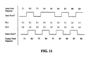
- FIG. 11 in conjunction with Figs. 9 and 10, a timing diagram illustrating the operation of field type detector 70 in the override mode is illustrated.
- the input signal is interlaced.
- the input signal becomes progressive.
- Microcontroller 26 detects the progressive signal and determines whether the first segment (e.g., a 240p frame) of the progressive signal is being stored in top field memory 18 or bottom field memory 20. If the first segment of the progressive signal is stored in bottom field memory 20 (as shown), microcontroller 26 sets registers 74 and 76 equal to the same value (e.g., L2) for the next segment of the progressive signal.
- the first segment e.g., a 240p frame
- Input BnotT low causes field 6 to overwrite the stale data in the top field memory 18 (i.e., the data corresponding to field 3). Afterwards, system microcontroller 26 alternates between allowing Input BnotT to go high and forcing Input BnotT to go low such that the progressive video data is written into top and bottom field memories 18 and 20. If the first segment of the progressive signal had been stored in top field memory 18 (not shown in FIG.
- microcontroller 26 would set register 74 equal to zero and set register 76 equal to or greater than the maximum value that counter 72 could reach before being reset by a Hsynch input. This would force Input BnotT high since the output of counter could never be less than the value stored in register 74 or greater than the value stored in register 76. Forcing Input BnotT high would cause the next segment of the progressive signal to overwrite the stale data in that would be present in the bottom field memory 20. Afterwards, system microcontroller 26 would alternately write the progressive signal into top and bottom field memories 18 and 20 in a manner similar to that shown in FIG. 11.
- a method of memory management for buffering digital video data of various formats i.e., progressive, interlaced, CCIR 601/656 compliant, and MPEG compliant formats) in a video memory that is partitioned into first and second buffers.
Landscapes
- Engineering & Computer Science (AREA)
- Multimedia (AREA)
- Signal Processing (AREA)
- Computer Graphics (AREA)
- Software Systems (AREA)
- Television Systems (AREA)
- Compression Or Coding Systems Of Tv Signals (AREA)
- Television Signal Processing For Recording (AREA)
- Data Exchanges In Wide-Area Networks (AREA)
Description
- The present invention relates to processing progressive video signals in digital TV receivers.
- US-A-5 327 235 and US-A- 5 430 488 describe systems for connecting video signals between progressive and interlaced formats.
- A standard Digital TV receiver architecture reuses MPEG digital video processing circuitry for the processing of digitized analog signals. Although this approach works well for processing digitized analog interlaced signals (e.g., NTSC and PAL signals having 480i or 1080i vertical formats), standard Digital TV receivers have difficulty processing the progressively scanned signals that are often produced by VCRs, video game consoles, and cable system text generators (e.g., progressively scanned signals having 240p vertical formats). The present invention is directed to overcoming this difficulty.
- A memory management process is for buffering digital video data of various formats (i.e., progressive, interlaced, CCIR 601/656 compliant, and MPEG compliant formats) in a video memory that is partitioned into first and second buffers.
- The invention is set out in the appended claims.
- In the Drawings:
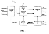
- FIG. 1 is a logical system block diagram of video processing circuitry of a standard Digital TV receiver;
- FIG. 2 is a timing diagram of the standard receiver processing an interlaced input signal;
- FIG. 3 is a timing diagram of the standard receiver processing a progressively scanned input signal;
- FIG. 4 is a logical system block diagram of video processing circuitry in accordance with the present invention;
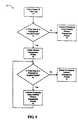
- FIG. 5 is a flow chart illustrating a method of processing a progressively scanned video signal in accordance with the present invention;
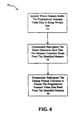
- FIG. 6 is a flow chart illustrating a video memory management method in accordance with the present invention;
- FIG. 7 is a timing diagram of an improved system processing a progressively scanned input signal in accordance with the video memory management method of FIG. 4;
- FIG. 8 is a flow chart illustrating an alternative memory management method in accordance with the present invention;
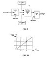
- FIG. 9 is a block diagram of field type detector circuitry of the video interface of FIG. 4; and
- FIG. 10 is a timing diagram for the field type detector circuitry of FIG. 9;
- FIG. 11 is a timing diagram of an improved system processing a progressively scanned input signal in accordance with the alternative memory management method of FIG. 8.
-
- The characteristics and advantages of the present invention will become more apparent from the following description, given by way of example.
- Referring to FIG. 1, the
video processing circuitry 10 of a standard Digital TV receiver is shown. Avideo input interface 12 is coupled to amemory 14 and amemory controller 16.Memory controller 16 controls the buffering of MPEG compliant video data, CCIR 601/656 compliant video data, and digitized analog signals inmemory 14, as described in further detail below. Araster generator 22 is also coupled tomemory controller 16 as well as to adisplay unit 24 that includes display format conversion circuitry and OSD overlay circuitry. -
Video input interface 12 is a video input port that manages the demuxing, sync processing, and field type detection of an input video signal.Video input interface 12 is capable of operating in two modes. One mode for receiving a CCIR 601/656 compliant bitstream and the other mode for receiving digitized analog signals. In the first mode,video input interface 12 extracts a known top/bottom field indication from a CCIR 601/656 compliant bitstream. In the second mode, blanking information is provided on Hsynch and Vsynch inputs ofvideo input interface 12 andvideo input interface 12 derives the top/bottom field indication from the relative timing of the Hsynch and Vsynch inputs. More specifically, for an interlaced signal the Vsynch input will toggle between aligning with the Hsynch input and occurring between consecutive Hsynch inputs. For a progressive signal the Vsynch input will not toggle and will either align with the Hsynch input or occur between consecutive Hsynch inputs. Thus, alternating top and bottom indicators will be derived for an interlaced signal and either top or bottom indicators will be derived for a progressive signal. Once the top/bottom field indication is extracted (in the case of a CCIR compliant bitstream) or derived (in the case of a digitized analog signal),video input interface 12 generates an Input BnotT signal based on the top/bottom field indication and passes the signal tomemory controller 16. More specifically, a field type detector (not shown) withinvideo input interface 12 generates a "high" Input BnotT signal in response to a bottom field indicator and generates a "low" Input BnotT signal in response to a top field indicator. - It should be noted that MPEG decoding circuitry (not shown to simplify the drawings) may be distinct from or integrated with
video input interface 12 for the decoding of an MPEG compliant bitstream, as known by those skilled in the art. During the decoding of an MPEG compliant bitstream,memory controller 16, in response to signals generated by the MPEG decoding circuitry, utilizesmemory 14 for buffering the incoming compressed bitstream, storing anchor frames, and for storing the decoded video frames. Once a frame of video has been stored inmemory 14 it is processed bydisplay unit 24 in the same fashion as the processing of the CCIR 601/656 compliant and interlaced video signals described below. -
Memory controller 16 manages the transfer of video data (e.g., MPEG compliant data, CCIR 601/656 compliant data, interlaced fields, and progressively scanned frames) to and frommemory 14. More specifically,memory 14 is partitioned into two buffers (top field memory 18 and bottom field memory 20) andmemory controller 16 manages the input of the video data to buffers 18 and 20 based upon the state of the Input BnotT signal transmitted byvideo input interface 12 or, in the case of the reception of an MPEG compliant datastream, based upon a signal generated by MPEG decoding circuitry.Memory controller 16 also manages the output of the stored video data frombuffers unit 24 which, in turn, processes the outputted data such that the data is adapted to a desired display format and combined with a desired OSD.Memory controller 16 manages the output of the video data frombuffers raster generator 22. - The Raster BnotT and Input BnotT signals are generated separately and may not be phase or frequency locked.
Video input interface 12 generates the Input BnotT signal based on the top/bottom field indicators extracted from a CCIR 601/656 compliant bitstream or derived from the relationship between the Hsynch and Vsynch inputs of a digitized analog signal (e.g., an interlaced or progressive signal).Raster generator 22 generates the Raster BnotT signal asynchronously from the Input BnotT signal. The Raster BnotT signal is an independent raster signal generated by counters driven from VCXO derived pixel clock. The Raster BnotT signal provides a stable drive signal to the deflection system ofdisplay unit 24 and controls the sequence of fields retrieved from memory. Although the asynchronous relationship between the Input BnotT and Raster BnotT signals does not interfere with the storage and retrieval of MPEG compliant data, CCIR 601/656 compliant data, and interlaced video data, the asynchronous relationship interferes with the storage and retrieval of progressively scanned video data (e.g., video data in a 240p vertical format), as shown below. - Referring now to FIG. 2, a timing diagram for the storage and retrieval of an interlaced signal is shown. More particularly, the relationship between the input video data, output video data, Input BnotT signal and Raster BnotT signal is shown. An indexed sequence of fields represents the memory location of the input and output video signal data, where T = top field memory and B = bottom field memory.
Memory controller 16 writes the input data intobottom field memory 20 upon reception of a "high" Input BnotT signal and writes the input data intotop field memory 18 upon reception of a "low" Input BnotT signal. Similarly,memory controller 16 reads the output data frombottom memory 16 upon reception of a "high" Raster BnotT signal and reads the output data fromtop field memory 18 upon reception of a "low" Raster BnotT signal. As shown in FIG. 2, the asynchronous relationship between the Input BnotT and Raster BnotT signals does not interfere with the proper storage and retrieval of video data for interlaced video signals. - Referring now to FIG. 3, a timing diagram illustrating the storage and retrieval of video data for an interlaced video signal followed by a progressive video signal is shown. Fields 1-4 correspond to fields of interlaced video data and are stored and retrieved from top and
bottom field memories Field 5 corresponds to a first frame of progressively scanned video data (e.g., a progressive video signal received from a game console or VCR that has been turned on by a user). AtField 5 the Input BnotT signal remains "high" indicating that the progressively scanned video data, for this exemplary timing diagram, has the same Hsynch/Vsynch relationship as the Field 4 portion of the interlaced video data. Since Input BnotT remains "high"memory controller 16 writes the frame of progressively scanned video data intobottom field memory 20. At fields 6 and 7memory controller 16 continues to write the frames of progressively scanned video data intobottom field memory 20 since the top/bottom indication associated with the frames of progressively scanned video data does not change. In response to the reception of the Raster BnotT signal,memory controller 16 correctly reads the fields of interlaced video data from memory 14 (fields 1-4). However,memory controller 16 incorrectly reads the frames of progressively scanned video data from memory 14 (fields 5-7). More specifically, atfields 5 and 7memory controller 16 reads stale video data from memory 14 (i.e., the interlaced video data of field 3) due to the reception of a "low" Raster BnotT signal fromraster generator 22. This stale data will continue to be read out oftop field memory 14 during the processing of the progressively scanned video data and will cause significant distortions in the video image displayed to a user. The present invention is directed to correcting this problem. - Referring now to FIG. 4, a block diagram of
video processing circuitry 30 of the present invention is shown and includes a system microcontroller 26 coupled to thevideo processing elements 10 of FIG. 1. More specifically, system microcontroller 26 is coupled tomemory controller 16,raster generator 22, anddisplay unit 24 such that video data in a progressively scanned format, an interlaced format, a CCIR 601/656 compliant format, or a MPEG compliant format is correctly stored in and retrieved frommemory 14. - Referring now to FIG. 5, in conjunction with FIG. 4, a
method 32 of processing progressively scanned video data is shown. The progressively scanned video data may be a 240p input generated by a video game console, VCR, cable system text generator, or the like. Initially, system microcontroller 26, atstep 34, determines the format of the video data received byvideo input interface 12 by reading the Input BnotT signal received bymemory controller 16. As explained above, when the Input BnotT signal toggles between high and low states the video format is not progressive (e.g., fields 1-4 of FIG. 3). When the Input BnotT signal remains constant (i.e., low or high) for two or more consecutive periods the video format is progressive (e.g., fields 5-7 of FIG. 3). It should be noted that system microcontroller 26 may determine if video data in an MPEG compliant format is being received by monitoring the signals generated by MPEG decoding circuitry, as known by those skilled in the art. Next, atstep 36, system microcontroller 26 determines if the video data is in a progressively scanned format. If not, system microcontroller 26, atstep 38, continues to process the video data using the standard memory management process described above. If so, system microcontroller 26, at step 40, modifies or partially overrides the memory management process in accordance with the present invention, as described in further detail below. Afterwards, atstep 42, system microcontroller 26 continues to monitor the Input BnotT signal received bymemory controller 16 to determine if the video data is still being received in a progressively scanned format. If not, system microcontroller 26, atstep 44, returns to the standard memory management process used for the processing of non-progressive video data. If so, system microcontroller 26, at step 46, continues to process the progressively scanned video data using the modified memory management process of step 40 and returns to step 42 to monitor the Input BnotT signal. - Referring now to FIGS. 6 and 7, in conjunction with FIG. 4, one
memory management process 50 of the present invention is shown. After the format of the video data received byvideo input interface 12 is identified as progressive, system microcontroller 26, atstep 52, monitors the state of the Input BnotT signal to identify which memory buffer (i.e.,top field memory 18 or bottom field memory 20) is being written with the progressively scanned video data. Once the memory is identified, system microcontroller 26, atstep 54, dynamically reprogramsraster generator 22 such thatmemory controller 16 correctly reads the progressively scanned video data from the identified memory buffer (i.e.,top field memory 18 or bottom field memory 20). As shown in the exemplary timing diagram of FIG. 7, if system microcontroller 26 determines that progressive video data is being written into bottom field memory 20 (i.e., the Input BnotT signal is "high"), system microcontroller 26 dynamically reprogramsraster generator 22 to output a "high" Raster BnotT signal. The "high" Raster BnotT signal will forcememory controller 16 to read the progressive video data frombottom field memory 20. System microcontroller 26, atstep 56, also dynamically reprogramsdisplay unit 24 to process the progressively scanned video data received from the identified memory buffer ofmemory 14. For example, system microcontroller 26 may dynamically reprogramdisplay unit 24 to convert a 240p signal retrieved frommemory 14 to 540p, 1080i, or some other vertical format required by a monitor or TV. - Turning now to FIG. 8, in conjunction with FIG. 4, an alternative
memory management process 60 of the present invention is shown. After the video data format received byvideo input interface 12 is identified as progressive, system microcontroller 26, atstep 62, monitors the state of the Input BnotT signal to identify which memory buffer (i.e.,top field memory 18 or bottom field memory 20) is being written with the progressively scanned video data. Next, atstep 64, system microcontroller 26 dynamically managesmemory controller 16 such thatmemory controller 16 alternately writes the progressively scanned video data into top andbottom field memories memory 14. - In order to force
memory controller 16 to alternately write the progressively scanned video data, system microcontroller 26 must override the Input BnotT signal. As stated previously, a field type detector withinVideo Input Interface 12 generates the Input BnotT signal. A block diagram of an exemplaryfield type detector 70 is shown in FIG. 9 and a timing diagram forfield type detector 70 is shown in FIG. 10.Field type detector 70 includes ahorizontal sample counter 72 having a pixel clock and Hsynch as inputs and having an output coupled to fieldtype detector logic 78. An input of fieldtype detector logic 78 is also coupled to an output of afirst register 74 which, in turn, is coupled to system microcontroller 26 (not shown in FIG. 9). Similarly, another input of fieldtype detector logic 78 is coupled to an output of asecond register 76 which, in turn, is coupled to system microcontroller 26 (not shown in FIG. 9). An output of fieldtype detector logic 78 is coupled to an input of alatch 80.Latch 80 generates the Input BnotT signal and is triggered by a Vsynch signal. - In operation,
horizontal sample counter 72 is driven by the input pixel clock and is reset and restarted by an Hsynch signal. The output ofcounter 72 is compared to system microcontroller programmable values L1 and L2 stored inregisters counter 72 is between value L1 and value L2 (during the time t1 < t < t2) the output of fieldtype detection logic 78 is high and the Input BnotT signal fromlatch 80 is high. In response to the high Input BnotT signal,memory controller 16 reads data intobottom field memory 20. During standard operation, if the output ofcounter 72 is below L1 or above L2 (during the time t<t1 OR t> t2) the output of fieldtype detection logic 78 is low and the input BnotT signal is low. As a result,memory controller 16 writes video data intotop field memory 18. - As described above, system microcontroller 26 detects the presence of progressively scanned video data by monitoring two or more identical Input BnotT signals. If a progressively scanned video signal is detected, the value of
registers memory controller 16 to write the progressively scanned video data into alternating top andbottom memories 18 and 20). - Turning to FIG. 11, in conjunction with Figs. 9 and 10, a timing diagram illustrating the operation of
field type detector 70 in the override mode is illustrated. For fields numbered 1 through 4, the input signal is interlaced. Atfield 5, the input signal becomes progressive. Microcontroller 26 detects the progressive signal and determines whether the first segment (e.g., a 240p frame) of the progressive signal is being stored intop field memory 18 orbottom field memory 20. If the first segment of the progressive signal is stored in bottom field memory 20 (as shown), microcontroller 26 sets registers 74 and 76 equal to the same value (e.g., L2) for the next segment of the progressive signal. This forces Input BnotT low on field 6 since the output of counter can never be between the values inregisters bottom field memories register 76 equal to or greater than the maximum value that counter 72 could reach before being reset by a Hsynch input. This would force Input BnotT high since the output of counter could never be less than the value stored inregister 74 or greater than the value stored inregister 76. Forcing Input BnotT high would cause the next segment of the progressive signal to overwrite the stale data in that would be present in thebottom field memory 20. Afterwards, system microcontroller 26 would alternately write the progressive signal into top andbottom field memories - Thus according to the principle of the present invention, there is provided a method of memory management for buffering digital video data of various formats (i.e., progressive, interlaced, CCIR 601/656 compliant, and MPEG compliant formats) in a video memory that is partitioned into first and second buffers.
Claims (12)
- A memory management process for buffering video signals in a memory partitioned into first and second buffers, the process including the steps of:characterised in that the process further comprises:receiving a video signal;generating a standard buffering signal (BnotT) in response to the reception of the video signal,processing the standard buffering signal to determine (34) if the received video signal is in a first format or in a second format;buffering (38) the received video signal in the memory in accordance with the standard buffering signal if the received video signal is in the first format, the first format video signal being alternately written into the first and second buffers and alternately read from the first and second buffers;partially overriding (36, 40) the standard buffering signal to generate a modified buffering signal if the received video signal is in a second format;buffering (40, 42, 46) the second format video signal in the memory in accordance with the modified buffering signal such that the second format video signal is buffered in the memory without the loss of data.
- The process of claim 1, wherein the second format is a digitised analog progressive (p) format or a 240p vertical format.
- The process of claim 1 or 2, wherein the received signal in the second format is generated by one of a video game console, a VCR, and a cable text generator.
- The process of any of claims 1 to 3, wherein the first format is one of an interlaced format, a CCIR 601/656 compliant format, and an MPEG compliant format.
- The process of any of claims 1 to 4, wherein the standard buffering signal includes a standard write signal and a standard read signal, the step of partially overriding the standard buffering signal to generate a modified buffering signal includes modifying the standard read signal, and the step of buffering the second format video signal in the memory in response to reception of the modified buffering signal includes the steps of:writing the second format video signal into one of the first or second buffers in accordance with the standard write signal;reading the second format video signal from one of the first or second buffers in accordance with the modified read signal.
- The process of any of claims 1 to 4, wherein the standard buffering signal includes a standard write signal and a standard read signal, the step of partially overriding the standard buffering signal to generate a modified buffering signal includes modifying the standard write signal, and the step of buffering the second format video signal in the memory in response to reception of the modified buffering signal includes the steps of:alternately writing the second format video signal into the first and second buffers in accordance with the modified write signal;alternately reading the second format video signal from the first and second buffers in accordance with the standard read signal.
- A buffering system in a digital TV receiver for processing video signals having a plurality of formats, the buffering system including:characterised in that the buffering system further comprises:a memory (14) for buffering the video signals, the memory having a first buffer (18) and a second buffer (20);means (12) for generating a standard buffering signal (BnotT) in response to the reception of a video signal,means (26) for processing the standard buffering signal to determine if the received video signal is in a first format or in a second format;means (16) for buffering the received video signal in the memory in accordance with the standard buffering signal if the received video signal is in the first format, the first format video signal being alternately written into the first and second buffers and alternately read from the first and second buffers;means (70) for partially overriding the standard buffering signal to generate a modified buffering signal if the received video signal is in a second format;means (16) for buffering the second format video signal in the memory in accordance with the modified buffering signal such that the second format video signal is buffered in the memory without the loss of data.
- The buffering system of claim 7, wherein the first format is one of an interlaced format, a CCIR 601/656 compliant format, and an MPEG compliant format.
- The buffering system of claim 7 or 8, wherein the second format is a digitised analog progressive (p) format or a 240p vertical format.
- The buffering system of any of claims 7 to 9, wherein the received signal in the second format is generated by one of a video game console, a VCR, and a cable text generator.
- The buffering system of any of claims 7 to 10, wherein the standard buffering signal includes a standard write signal and a standard read signal, the modified buffering signal includes the standard write signal and a modified read signal, and the means for buffering the second format video signal further includes:means for writing the second format video signal into one of the first or second buffers in accordance with the standard write signal;means for reading the second format video signal from one of the first or second buffers in accordance with the modified read signal.
- The buffering system of any of claims 7 to 10, wherein the standard buffering signal includes a standard write signal and a standard read signal, the modified buffering signal includes a modified write signal and the standard read signal, and the means for buffering the second format video signal further includes:means for alternately writing the second format video signal into the first and second buffers in accordance with the modified write signal;means for alternately reading the second format video from the first and second buffers in accordance with the standard read signal.
Applications Claiming Priority (2)
| Application Number | Priority Date | Filing Date | Title |
|---|---|---|---|
| US14415299P | 1999-07-15 | 1999-07-15 | |
| US144152 | 1999-07-15 |
Publications (3)
| Publication Number | Publication Date |
|---|---|
| EP1069768A2 EP1069768A2 (en) | 2001-01-17 |
| EP1069768A3 EP1069768A3 (en) | 2002-06-26 |
| EP1069768B1 true EP1069768B1 (en) | 2004-09-22 |
Family
ID=22507311
Family Applications (1)
| Application Number | Title | Priority Date | Filing Date |
|---|---|---|---|
| EP00114589A Expired - Lifetime EP1069768B1 (en) | 1999-07-15 | 2000-07-07 | Processing of progressive video signals in digital TV receivers |
Country Status (8)
| Country | Link |
|---|---|
| US (1) | US6633344B1 (en) |
| EP (1) | EP1069768B1 (en) |
| JP (1) | JP4515607B2 (en) |
| KR (1) | KR100671985B1 (en) |
| CN (1) | CN1226876C (en) |
| DE (1) | DE60013968T2 (en) |
| MX (1) | MXPA00006970A (en) |
| MY (1) | MY125108A (en) |
Families Citing this family (7)
| Publication number | Priority date | Publication date | Assignee | Title |
|---|---|---|---|---|
| US6559890B1 (en) * | 1999-04-21 | 2003-05-06 | Ascent Media Group, Inc. | Methods and apparatus for correction of 2-3 field patterns |
| US20040061530A1 (en) * | 2002-08-12 | 2004-04-01 | Satoru Tanigawa | Clock conversion apparatus, clock conversion method, video display apparatus, and memory address setting method |
| US7301582B2 (en) * | 2003-08-14 | 2007-11-27 | Broadcom Corporation | Line address computer for providing line addresses in multiple contexts for interlaced to progressive conversion |
| WO2006129280A2 (en) * | 2005-06-03 | 2006-12-07 | Nxp B.V. | Video decoder with hybrid reference texture |
| US8072443B2 (en) * | 2005-06-29 | 2011-12-06 | Intel Corporation | Techniques to switch between video display modes |
| US20080030615A1 (en) * | 2005-06-29 | 2008-02-07 | Maximino Vasquez | Techniques to switch between video display modes |
| JP2008301014A (en) | 2007-05-30 | 2008-12-11 | Fujifilm Corp | Photographing apparatus and method, and program |
Family Cites Families (18)
| Publication number | Priority date | Publication date | Assignee | Title |
|---|---|---|---|---|
| DE3719496A1 (en) | 1987-06-11 | 1988-12-29 | Bosch Gmbh Robert | STORAGE ARRANGEMENT FOR A DIGITAL VIDEO TAPE |
| JP2698105B2 (en) | 1987-07-28 | 1998-01-19 | 三洋電機株式会社 | Digital television receiver |
| JP2559478B2 (en) | 1988-10-14 | 1996-12-04 | 株式会社日立製作所 | Video memory circuit |
| JP3020528B2 (en) * | 1989-12-14 | 2000-03-15 | キヤノン株式会社 | Image processing device |
| US5170251A (en) * | 1991-05-16 | 1992-12-08 | Sony Corporation Of America | Method and apparatus for storing high definition video data for interlace or progressive access |
| KR0159109B1 (en) * | 1991-09-19 | 1999-01-15 | 강진구 | Converter of aspect ratio and scan line number |
| GB2260053B (en) * | 1991-09-27 | 1995-03-08 | Sony Broadcast & Communication | Image signal processing |
| GB2264417B (en) * | 1992-02-17 | 1995-12-06 | Sony Broadcast & Communication | Video standards conversion |
| JP3154190B2 (en) * | 1992-04-10 | 2001-04-09 | ソニー株式会社 | General-purpose scanning cycle converter |
| US5861894A (en) | 1993-06-24 | 1999-01-19 | Discovision Associates | Buffer manager |
| JPH07236117A (en) | 1994-02-24 | 1995-09-05 | Nec Corp | Picture processor |
| US5610661A (en) | 1995-05-19 | 1997-03-11 | Thomson Multimedia S.A. | Automatic image scanning format converter with seamless switching |
| JP3378710B2 (en) | 1995-10-16 | 2003-02-17 | 三洋電機株式会社 | Reduced image writing / reading method and reduced image processing circuit |
| JP3617573B2 (en) * | 1996-05-27 | 2005-02-09 | 三菱電機株式会社 | Format conversion circuit and television receiver including the format conversion circuit |
| GB9704027D0 (en) * | 1997-02-26 | 1997-04-16 | Discovision Ass | Memory manager for mpeg decoder |
| US6177922B1 (en) * | 1997-04-15 | 2001-01-23 | Genesis Microship, Inc. | Multi-scan video timing generator for format conversion |
| US5949441A (en) * | 1997-08-01 | 1999-09-07 | International Business Machines Corporation | Multimedia terminal with an encoder for converting analog video data to compressed digitized video data |
| US6297848B1 (en) * | 1998-11-25 | 2001-10-02 | Sharp Laboratories Of America, Inc. | Low-delay conversion of 3:2 pulldown video to progressive format with field averaging |
-
2000
- 2000-05-31 US US09/584,148 patent/US6633344B1/en not_active Expired - Lifetime
- 2000-07-07 EP EP00114589A patent/EP1069768B1/en not_active Expired - Lifetime
- 2000-07-07 DE DE60013968T patent/DE60013968T2/en not_active Expired - Lifetime
- 2000-07-10 KR KR1020000039190A patent/KR100671985B1/en not_active IP Right Cessation
- 2000-07-11 MY MYPI20003170 patent/MY125108A/en unknown
- 2000-07-14 MX MXPA00006970A patent/MXPA00006970A/en active IP Right Grant
- 2000-07-14 CN CNB001203746A patent/CN1226876C/en not_active Expired - Fee Related
- 2000-07-14 JP JP2000213844A patent/JP4515607B2/en not_active Expired - Fee Related
Also Published As
| Publication number | Publication date |
|---|---|
| MXPA00006970A (en) | 2003-12-12 |
| MY125108A (en) | 2006-07-31 |
| KR100671985B1 (en) | 2007-01-19 |
| CN1281312A (en) | 2001-01-24 |
| US6633344B1 (en) | 2003-10-14 |
| EP1069768A3 (en) | 2002-06-26 |
| KR20010015258A (en) | 2001-02-26 |
| DE60013968D1 (en) | 2004-10-28 |
| JP4515607B2 (en) | 2010-08-04 |
| DE60013968T2 (en) | 2005-10-13 |
| CN1226876C (en) | 2005-11-09 |
| JP2001069422A (en) | 2001-03-16 |
| EP1069768A2 (en) | 2001-01-17 |
Similar Documents
| Publication | Publication Date | Title |
|---|---|---|
| US7589789B2 (en) | Video converting device and method for digital TV | |
| US5917552A (en) | Video signal interface system utilizing deductive control | |
| AU755005B2 (en) | Receiver for simultaneously displaying signals having different display formats and/or different frame rates and method thereof | |
| US7038728B2 (en) | Image display method and apparatus | |
| KR101083943B1 (en) | Information transmitting apparatus and method, information receiving apparatus and method, information transmitting and receiving system and method, recording medium and program | |
| US7542097B2 (en) | Video signal processing apparatus and method | |
| EP0743788A1 (en) | Automatic image scanning format converter with seamless switching | |
| US20020008780A1 (en) | Apparatus and method for converting multi-source input images | |
| US6577348B1 (en) | Apparatus and method for digitizing an analog video signal | |
| US6492982B1 (en) | Image display control method and apparatus | |
| US7268820B2 (en) | Video signal conversion apparatus delivering enhanced display quality for video signals from film and video sources | |
| US20050104899A1 (en) | Real time data stream processor | |
| KR20000069754A (en) | Device for receiving, displaying and simultaneously recording television images via a buffer | |
| US6297850B1 (en) | Sync signal generating apparatus and method for a video signal processor | |
| EP1069768B1 (en) | Processing of progressive video signals in digital TV receivers | |
| US5896177A (en) | Device for controlling an aspect ratio in tv-monitor integrated wide screen receiver | |
| US5680176A (en) | Apparatus for controlling caption display on a wide aspect ratio | |
| JPH10336595A (en) | Decoder | |
| US20030007090A1 (en) | Video-signal processing apparatus and method, recording medium and program | |
| AU770732B2 (en) | Apparatus for converting video format and method therefor | |
| JP2001268473A (en) | Television broadcast receiver | |
| US20030174244A1 (en) | Image format conversion device with reduced line memory capacity | |
| US6819363B2 (en) | Video signal processing device | |
| JPH089343A (en) | Video signal converter | |
| JP3043198B2 (en) | Scan conversion circuit |
Legal Events
| Date | Code | Title | Description |
|---|---|---|---|
| PUAI | Public reference made under article 153(3) epc to a published international application that has entered the european phase |
Free format text: ORIGINAL CODE: 0009012 |
|
| AK | Designated contracting states |
Kind code of ref document: A2 Designated state(s): AT BE CH CY DE DK ES FI FR GB GR IE IT LI LU MC NL PT SE |
|
| AX | Request for extension of the european patent |
Free format text: AL;LT;LV;MK;RO;SI |
|
| PUAL | Search report despatched |
Free format text: ORIGINAL CODE: 0009013 |
|
| AK | Designated contracting states |
Kind code of ref document: A3 Designated state(s): AT BE CH CY DE DK ES FI FR GB GR IE IT LI LU MC NL PT SE |
|
| AX | Request for extension of the european patent |
Free format text: AL;LT;LV;MK;RO;SI |
|
| 17P | Request for examination filed |
Effective date: 20020827 |
|
| AKX | Designation fees paid |
Designated state(s): DE FR GB IT |
|
| 17Q | First examination report despatched |
Effective date: 20030430 |
|
| GRAP | Despatch of communication of intention to grant a patent |
Free format text: ORIGINAL CODE: EPIDOSNIGR1 |
|
| GRAS | Grant fee paid |
Free format text: ORIGINAL CODE: EPIDOSNIGR3 |
|
| GRAA | (expected) grant |
Free format text: ORIGINAL CODE: 0009210 |
|
| AK | Designated contracting states |
Kind code of ref document: B1 Designated state(s): DE FR GB IT |
|
| REG | Reference to a national code |
Ref country code: GB Ref legal event code: FG4D |
|
| REG | Reference to a national code |
Ref country code: IE Ref legal event code: FG4D |
|
| REF | Corresponds to: |
Ref document number: 60013968 Country of ref document: DE Date of ref document: 20041028 Kind code of ref document: P |
|
| PLBE | No opposition filed within time limit |
Free format text: ORIGINAL CODE: 0009261 |
|
| STAA | Information on the status of an ep patent application or granted ep patent |
Free format text: STATUS: NO OPPOSITION FILED WITHIN TIME LIMIT |
|
| ET | Fr: translation filed | ||
| 26N | No opposition filed |
Effective date: 20050623 |
|
| PGFP | Annual fee paid to national office [announced via postgrant information from national office to epo] |
Ref country code: IT Payment date: 20070730 Year of fee payment: 8 |
|
| PG25 | Lapsed in a contracting state [announced via postgrant information from national office to epo] |
Ref country code: IT Free format text: LAPSE BECAUSE OF NON-PAYMENT OF DUE FEES Effective date: 20080707 |
|
| PGFP | Annual fee paid to national office [announced via postgrant information from national office to epo] |
Ref country code: FR Payment date: 20110726 Year of fee payment: 12 |
|
| PGFP | Annual fee paid to national office [announced via postgrant information from national office to epo] |
Ref country code: GB Payment date: 20110726 Year of fee payment: 12 Ref country code: DE Payment date: 20110713 Year of fee payment: 12 |
|
| GBPC | Gb: european patent ceased through non-payment of renewal fee |
Effective date: 20120707 |
|
| REG | Reference to a national code |
Ref country code: FR Ref legal event code: ST Effective date: 20130329 |
|
| PG25 | Lapsed in a contracting state [announced via postgrant information from national office to epo] |
Ref country code: DE Free format text: LAPSE BECAUSE OF NON-PAYMENT OF DUE FEES Effective date: 20130201 Ref country code: GB Free format text: LAPSE BECAUSE OF NON-PAYMENT OF DUE FEES Effective date: 20120707 Ref country code: FR Free format text: LAPSE BECAUSE OF NON-PAYMENT OF DUE FEES Effective date: 20120731 |
|
| REG | Reference to a national code |
Ref country code: DE Ref legal event code: R119 Ref document number: 60013968 Country of ref document: DE Effective date: 20130201 |