EP1069573B1 - Ferroelectric memory device with reset circuit - Google Patents
Ferroelectric memory device with reset circuit Download PDFInfo
- Publication number
- EP1069573B1 EP1069573B1 EP00118131A EP00118131A EP1069573B1 EP 1069573 B1 EP1069573 B1 EP 1069573B1 EP 00118131 A EP00118131 A EP 00118131A EP 00118131 A EP00118131 A EP 00118131A EP 1069573 B1 EP1069573 B1 EP 1069573B1
- Authority
- EP
- European Patent Office
- Prior art keywords
- bit line
- memory cell
- bit lines
- reset circuit
- controlling signal
- Prior art date
- Legal status (The legal status is an assumption and is not a legal conclusion. Google has not performed a legal analysis and makes no representation as to the accuracy of the status listed.)
- Expired - Lifetime
Links
Images


Classifications
-
- G—PHYSICS
- G11—INFORMATION STORAGE
- G11C—STATIC STORES
- G11C11/00—Digital stores characterised by the use of particular electric or magnetic storage elements; Storage elements therefor
- G11C11/21—Digital stores characterised by the use of particular electric or magnetic storage elements; Storage elements therefor using electric elements
- G11C11/22—Digital stores characterised by the use of particular electric or magnetic storage elements; Storage elements therefor using electric elements using ferroelectric elements
Definitions
- the present invention relates to a ferroelectric memory device that is not liable to cause a malfunction by applying an electric field to the ferroelectric capacitor.
- a ferroelectric memory device to realize nonvolate stored data by using a ferroelectric material in the capacitor of the memory cell has been proposed.
- the ferroelectric capacitor has a hysteresis characteristic and thus a remanence having a different polarity remains even when the electric field is zero, according to the magnetic history.
- a nonvolatile memory device can be realized.
- a main body memory cell comprises one transistor and one capacitor (1T1C) per one bit.
- one dummy memory cell reference cell
- main body memory cells normal cells
- a main body memory cell comprises two transistors and two capacitors (2T2C) per one bit without having a dummy memory cell. That is, one pair of complementary data is stored in one pair of ferroelectric capacitors.
- the preamble of claim 1 is based on such a 2T2C main body memory cell.
- ferroelectric materials to form a capacitor KNO 3 , PbLa 2 O 3 -ZrO 2 -TiO 2 and PbTiO 3 -PbZrO 3 are known.
- a ferromagnetic material having a fatigue much smaller than that of PbTiO 3 -PbZrO 3 and thus suitable for a ferroelectric memory device is disclosed in the official gazette of the PCT international publication No. WO93/12542.
- the dummy memory cell capacitor has a capacity, namely an area, at least double that of the main body memory cell capacitor.
- the main body memory cell capacitor reverses polarity and returns to the original polarity state, or keeps the original polarity state without reversal according to the stored data at the time of the readout.
- the dummy memory cell capacitor maintains the original polarity state without reversal regardless of the stored data in the main body memory cell. That is, the main body memory cell capacitor applies the voltage between the electrodes in both the plus and minus polarities, whereas the dummy memory cell capacitor applies the voltage between the electrodes always in one polarity.
- the voltage applied to the cell plate electrode of the main body memory cell capacitor, the voltage applied to the cell plate electrode (dummy cell plate electrode) of the dummy memory cell capacitor, the voltage applied to the word line connected to the gate electrode of the main body memory cell transistor, and the voltage applied to the word line (dummy word line) connected to the gate electrode of the dummy memory cell transistor are all 5 V, which is equal to the power source voltage.
- a voltage is applied to the word line and the cell plate electrode at the same time. Besides, regardless of stored data of the main body memory cell, after switching the voltage of the cell plate electrode of the main body memory cell capacitor off, the voltage of the word line and the dummy word line is turned off and then the bit line is precharged. Furthermore, when the voltage of the word line and the dummy word line is turned off, the voltage of the cell plate electrode of the dummy memory cell capacitor is turned off at the same time.
- the word line is turned off in a conventional 1T1C type ferroelectric memory device with the electric field remains in the capacitor as mentioned above, the state in which the electric field remains in the capacitor continues.
- the electric field stress is applied on the capacitor, and thus particularly under conditions of high voltage or high temperature, it provides a factor in deteriorating the capacitor.
- the cell plate potential may become negative when the driving ability of the cell plate is small. In this case, the "L" data of the memory cell capacitor connected to the cell plate may be destroyed.
- An object of the present invention is to alleviate the effect of the electric field applied to the ferroelectric capacitor and prevent the malfunction of the ferroelectric memory device.
- FIG. 1 A circuit configuration of a first embodiment of the ferroelectric memory devices not included by the present invention is illustrated in FIG. 1.
- the operation timing of this ferroelectric memory device is shown in FIG. 2.
- the memory cell of the ferroelectric memory device stores data of one bit with one transistor and one ferroelectric capacitor.
- WL0 to WL 255 represent word lines; DWL0 and DWL1 dummy word lines; BL and /BL bit lines; CP a cell plate electrode; DCP a dummy cell plate electrode; BP a bit line precharge controlling signal; DCRST a dummy memory cell data initializing controlling signal; SAE a sense amplifier controlling signal; VSS a ground voltage; SA a sense amplifier; C0 to C255 main body memory cell capacitors; DC0 and DC1 dummy memory cell capacitors; Qn0 to Qn255, QnD0 to QnD1, QnR0 to QnR1, and QuBP0 to QnBP1 N channel type MOS transistors.
- Qn0 to Qn255 are called main body memory cell transistors and QnD0 to QnD1 are called dummy memory cell transistors.
- bit lines BL, /BL are connected to the sense amplifier SA.
- the sense amplifier SA is controlled by the sense amplifier controlling signal SAE.
- the first electrode of the dummy memory cell capacitor DC0 is connected to the bit line /BL via the dummy memory cell transistor QnD0 whose gate electrode is connected to the dummy word line DWL0, and the second electrode thereof is connected to the dummy cell plate electrode DCP.
- the first electrode of the dummy memory cell capacitor DC1 is connected to the bit line BL via the dummy memory cell transistor QnD1 whose gate electrode is connected to the word line DWL1, and the second electrode thereof is connected to the dummy cell plate electrode DCP.
- the first electrodes of the dummy memory cell capacitors DC0, DC1 are connected to the ground voltage VSS, which is the dummy memory cell data initializing voltage, via the N channel type MOS transistors QnR0, QnR1 to which gate electrode the dummy memory cell data initializing controlling signal DCRST is applied.
- the first electrode of the main body memory cell capacitor C0 is connected to the bit line BL via the main body memory cell transistor Qn0 whose gate electrode is connected to the word line WL0 and the second electrode thereof is connected to the cell plate electrode CP.
- the first electrode of the main body memory cell capacitor C1 is connected to the bit line /BL via the main body memory cell transistor Qn1 whose gate electrode is connected to the word line WL1, and the second electrode thereof is connected to the cell plate electrode CP.
- bit line precharge controlling signal BP is made to be a logical voltage "H” and accordingly the bit lines BL, /BL are made to be a logical voltage "L”. Further, the word lines WL0 to WL255, the dummy word lines DWL0 to DWL1, the cell plate electrode CP, and the dummy cell plate electrode DCP are made to be the logical voltage "L”. And the dummy memory cell data initializing controlling signal DCRST is made to be the logical voltage "H” to initialize the dummy memory cell capacitors DC0 and DC1.
- bit line precharge controlling signal BP to assume the logical voltage "L”
- bit lines BL, /BL come into the floating state
- DCRST the dummy memory cell data initializing controlling signal
- the word line WL0, the dummy word line DWL0, the cell plate electrode CP and the dummy cell plate electrode DCP are changed to the logical voltage "H"
- the data in the main body memory cell capacitor C0 are read out to the bit line BL
- the data in the dummy memory cell capacitor DC0 are read out to the bit line /BL.
- the sense amplifier controlling signal SAE is changed to the logical voltage "H” to operate the sense amplifier SA. Then by changing the cell plate electrode CP to the logical voltage "L”, the data of the main body memory cell capacitor C0 are rewritten. By changing the dummy word line DWL0 to assume the logical voltage "L”, the dummy memory cell capacitor DC0 is detached from the bit line /BL. By changing the sense amplifier controlling signal SAE to the logical voltage "L”, the operation of the sense amplifier SA is stopped. By changing the bit line precharge controlling signal BP to the logical voltage "H”, the bit lines BL, /BL assume the ground voltage VSS.
- the dummy cell plate electrode DCP is changed to the logical voltage "L” to make the electric field applied on the dummy memory cell capacitor DC0 zero. Further, by changing the word line WL0 to be the logical voltage "L”, the main body memory cell capacitor C0 is detached from the bit lines BL, /BL. With this operation, reading out and rewriting of the data can be finished in the state in which an electric field is not applied to the main body memory cell capacitor C0 and the dummy memory cell capacitor DC0.
- the circuit configuration and the operation timing described herein represent just one example, and thus it is sufficient if only the electric field on the memory cell capacitor satisfies the above mentioned relationship.
- ferroelectric memory device of this embodiment includes that rewriting of the data is finished in the state in which a load does not remain nor is an electric field applied on the memory cell capacitor. If the word line is changed to be the logical voltage "L" before precharging the bit line to the ground voltage VSS, a load remains in the memory cell capacitor and thus an electric field continues to be on the memory cell capacitor until the load is eliminated by leakage or some other reason. In this case, the memory cell capacitor may deteriorate.
- the life of the capacitor can extend to 10 times.
- the life is determined by the entire operation time regardless of the cycle time.
- the ferroelectric memory cell stores data of one bit with one transistor and one ferroelectric capacitor.
- the ferroelectric memory cell of a second embodiment stores data of one bit with two transistors and two ferroelectric capacitors so that complementary data are stored in ferroelectric capacitors respectively.
- a circuit configuration of the second embodiment of the ferroelectric memory devices of the present invention is illustrated in FIG. 3. The operation timing of this ferroelectric memory device is shown in FIG. 4.
- WL0 to WL 255 represent word lines; BL and /BL bit lines; CP a cell plate electrode; BP a bit line precharge controlling signal; SAE a sense amplifier controlling signal; VSS a ground voltage; SA a sense amplifier; C0 to C255, C0B to C255B memory cell capacitors; Qn0 to Qn255, Qn0B to Qn255B, QnBP0 to QnBP2 N channel type MOS transistors.
- bit lines BL, /BL are connected to the sense amplifier SA.
- the sense amplifier SA is controlled by the sense amplifier controlling signal SAE.
- the first electrode of the memory cell capacitor C0 is connected to the bit line BL via the memory cell transistor Qn0 whose gate electrode is connected to the word line WL0, and the second electrode thereof is connected to the cell plate electrode CP.
- the first electrode of the memory cell capacitor C0B which is the companion to the memory cell capacitor C0, is connected to the bit line /BL via the memory cell transistor Qn0B whose gate electrode is connected to the word line WL0, and the second electrode thereof is connected to the cell plate electrode CP.
- the connections of the other memory cell capacitors C1 to C255 and C1B to C255B are the same as the above mentioned memory cell capacitors C0 and C0B.
- the bit lines BL, /BL are connected by the N channel type MOS transistor QnBP2.
- the bit line BL and the ground voltage VSS, and the bit line /BL and the ground voltage VSS are connected by the N channel type MOS transistors QnBP0, QnBP2 respectively.
- the gate electrodes of the N channel type MOS transistors QnBP0 to QnBP1 are connected to the bit line precharge controlling signal BP.
- the operation timing of the ferroelectric memory device will be explained with reference to the operation timing chart of FIG. 4.
- the bit line precharge controlling signal BP is made to assume a logical voltage "H” and accordingly the bit lines BL, /BL assume a logical voltage "L” to read out the data in the memory cell.
- the word lines WL0 to WL255 and the cell plate electrode CP assume the ground voltage VSS, which is the logical voltage "L”.
- bit line precharge controlling signal BP to assume the logical voltage "L”
- bit lines BL, /BL come into the floating state
- word line WL0 and the cell plate electrode CP to the logical voltage "H”
- the data in the main body memory cell capacitors C0, C0B are read out to the bit lines BL, /BL.
- the sense amplifier controlling signal SAE is changed to the logical voltage "H” to operate the sense amplifier SA.
- cell plate electrode CP to the logical voltage "L”
- the data of the memory cell capacitors C0 and C0B are rewritten.
- the memory cell capacitors C0 and C0B are detatched from the bit lines BL, /BL. With this operation, reading out and rewriting the data can be finished in the state in which an electric field is not applied on the main body memory cell capacitors C0 and C0B.
- the circuit configuration and the operation timing described herein represents just one example, and thus it is sufficient if only the electric field on the memory cell capacitor satisfies the above mentioned relationship.
- ferroelectric memory device of this embodiment includes that rewriting of the data is finished in the state in which a load does not remain nor is an electric field applied on the memory cell capacitors as in the first embodiment. That is, by shortening the time during which an electric field is applied on the memory cell capacitors, the deterioration of the memory cell capacitor can be prevented to prolong its life.
- the state in which a load does not remain in the memory cell capacitor was achieved after rewriting, whereas in the third embodiment, the state can be realized before initiating reading out as well.
- the ferroelectric memory device of the third embodiment stores data of one bit with two transistors and two ferroelectric capacitors.
- a configuration like the first embodiment in that the ferroelectric memory device stores data of one bit with one transistor and one ferroelectric capacitor can be employed as well. Since the circuit configuration of the ferroelectric memory device is the same as that of the second embodiment illustrated in FIG. 3, details of the circuit are not described herein.
- the bit line precharge controlling signal BP is made to assume a logical voltage "H” and accordingly the bit lines BL, /BL assume a logical voltage "L” to read out the data in the memory cell.
- the word lines WL0 to WL255, the cell plate electrode CP assume the ground voltage VSS, which is the logical voltage "L”.
- the sense amplifier controlling signal SAE By changing the sense amplifier controlling signal SAE to assume the logical voltage "L”, the operation of the sense amplifier SA is stopped. Then by changing the bit line precharge controlling signal BP to the logical voltage "H”, the bit lines BL, /BL assume the ground voltage VSS. The state in which an electric field is not applied to the memory cell capacitors C0 and C0B can be realized. By changing the word line WL0 to the logical voltage "L”, the memory cell capacitors C0 and C0B are detached from the bit lines BL, /BL. With this operation, reading out and rewriting the data can be finished in the state in which an electric field is not applied on the memory cell capacitors C0 and C0B.
- ferroelectric memory device of this embodiment includes that rewriting of the data is finished in the state in which a load does not remain nor is an electric field applied on the memory cell capacitors as in the second embodiment. And further, since the electric field across the electrodes of the memory cell capacitor is zero before reading out the data, the voltage in the electrode in the floating state, which is opposite to the cell plate electrode can be reset. Thus, the data can be read out stably.
- FIG. 6 A circuit configuration of a fourth embodiment of the ferroelectric memory devices not included by the present invention is illustrated in FIG. 6.
- the operation timing of the ferroelectric memory device is shown in FIG. 7.
- the memory cell of the ferroelectric memory device stores data of one bit with one transistor and one ferroelectric capacitor.
- WL0 to WL 255 represent word lines; DWL0 to DWL1 dummy word lines; BL and /BL bit lines; CP a cell plate electrode; DCP a dummy cell plate electrode; BP a bit line precharge controlling signal; SAE a sense amplifier controlling signal; VSS a ground voltage; SA a sense amplifier; C0 to C255 main body memory cell capacitors; DC0 to DC1 dummy memory cell capacitors; Qn0 to Qn255, QnD0 to QnD1, and QnBP0 to QnBP1 N channel type MOS transistors.
- Qn0 to Qn255 are called main body memory cell transistors and QnD0 to QnD1 are called dummy memory cell transistors.
- bit lines BL, /BL are connected to the sense amplifier SA.
- the sense amplifier SA is controlled by the sense amplifier controlling signal SAE.
- the first electrode of the dummy memory cell capacitor DC0 is connected to the bit line /BL via the dummy memory cell transistor QnD0 whose gate electrode is connected to the dummy word line DWL0.
- the second electrode of DC0 is connected to the dummy cell plate electrode DCP.
- the first electrode of the dummy memory cell capacitor DC1 is connected to the bit line BL via the dummy memory cell transistor QnD1 whose gate electrode is connected to the word line DWL1.
- the second electrode of DC1 is connected to the dummy cell plate electrode DCP.
- the first electrode of the main body memory cell capacitor C0 is connected to the bit line BL via the main body memory cell transistor Qn0 whose gate electrode is connected to the word line WL0.
- the second electrode of C0 is connected to the cell plate electrode CP.
- the first electrode of the main body memory cell capacitor C1 is connected to the bit line /BL via the main body memory cell transistor Qn1 whose gate electrode is connected to the word line WL1.
- the second electrode of C1 is connected to the cell plate electrode CP.
- bit line precharge controlling signal BP is made to assume a logical voltage "H” and accordingly the bit lines BL, /BL assume a logical voltage "L”. Further, the word lines WL0 to WL255, the dummy word lines DWL0 to DWL1, the cell plate electrode CP, and the dummy cell plate electrode DCP assume the logical voltage "L”.
- bit lines BL, /BL come into the floating state.
- word line WL0, the dummy word line DWL0, the cell plate electrode CP and the dummy cell plate electrode DCP are changed to the logical voltage "H"
- the data in the main body memory cell capacitor C0 are read out to the bit line BL
- the data in the dummy memory cell capacitor DC0 are read out to the bit line /BL.
- the sense amplifier controlling signal SAE is changed to the logical voltage "H” to operate the sense amplifier SA. Then by changing the cell plate electrode CP to the logical voltage "L”, the data of the main body memory cell capacitor C0 are rewritten. By changing the sense amplifier controlling signal SAE to the logical voltage "L”, the operation of the sense amplifier SA is stopped. By changing the bit line precharge controlling signal BP to the logical voltage "H”, the bit lines BL, /BL are made to assume the ground voltages VSS. In the above mentioned conditions the state in which an electric field is not applied to the main body memory cell capacitor C0 can be achieved.
- the dummy cell plate electrode DCP is changed to the logical voltage "L” to make the electric field applied to the dummy memory cell capacitor DC0 zero. Further, by changing the word line WL0 and the dummy word line DWL0 to the logical voltage "L”, the main body memory cell capacitor C0 and the dummy memory cell capacitor DC0 are detatched from the bit line /BL. With this operation, reading out and rewriting the data can be finished in the state in which an electric field is not applied on the main body memory cell capacitor C0 and the dummy memory cell capacitor DC0.
- circuit configuration and the operation timing described herein represents just one example, and thus it is sufficient if only the electric field on the memory cell capacitor satisfies the above mentioned relationship. Further, a configuration in combination with the above mentioned third embodiment to realize the state in which an electric field is not applied on the both electrodes of the memory cell capacitors before reading out the information can be employed as well.
- ferroelectric memory device of this embodiment includes that rewriting of the data is finished in the state in which a load does not remain nor an electric field is applied on the memory cell capacitor as in the first embodiment.
- a controlling signal to initialize the dummy memory cell data and an N channel type MOS transistor are necessary in the first embodiment, a circuit element for initializing the dummy memory cell data is unnecessary in this embodiment.
- FIG. 8 A circuit configuration of a fifth embodiment of the ferroelectric memory devices of the present invention is illustrated in FIG. 8, and the operation timing of the ferroelectric memory device is shown in FIG. 9.
- the memory cell of the ferroelectric memory device includes independent bit line precharge (BP) and bit line equalize (BP2) portions.
- bit lines BL, /BL are connected to the sense amplifier SA.
- the sense amplifier SA is controlled by the sense amplifier controlling signal SAE.
- the first electrode of the memory cell capacitor C0 is connected to the bit line BL via the memory cell transistor Qn0 whose gate electrode is connected to the word line WL0.
- the second electrode of C0 is connected to the cell plate electrode CP.
- the first electrode of the memory cell capacitor C0B which is the companion to the memory cell capacitor C0, is connected to the bit line /BL via the memory cell transistor Qn0B whose gate electrode is connected to the word line WL0.
- the second electrode of C0B is connected to the cell plate electrode CP.
- the connections of the other memory cell capacitors C1 to C255 and C1B to C255B are the same as the above mentioned memory cell capacitors C0 and C0B.
- the bit lines BL, /BL are connected with the N channel type MOS transistor QnBP2.
- the bit line BL and the ground voltage VSS, and the bit line /BL and the ground voltage VSS are connected with the N channel type MOS transistors QnBP0, QnBP1 respectively.
- the gate electrodes of the N channel type MOS transistors QnBP0 and QnBP1 are connected to the bit line precharge controlling signal BP, and the gate electrode of the N channel type MOS transistor QnBP2 is connected to the bit line equalize controlling signal BP2.
- the bit line precharge controlling signal BP and bit line equalizing control signal BP2 are made to assume logical voltage "H” and accordingly the bit lines BL, /BL assume a logical voltage "L” to read out the data in the memory cell.
- the word lines WL0 to WL255 and the cell plate electrode CP are made to assume the ground voltage VSS, which is the logical voltage "L”. Then by changing the bit line precharge controlling signals BP, BP2 to be the logical voltage "L”, the bit lines BL, /BL come into the floating state.
- bit lines BL, /BL are made to be the ground voltages VSS.
- the state in which an electric field is not applied to the main body memory cell capacitors C0 and C0B can be achieved.
- the word line WL0 to the logical voltage "L” the memory cell capacitors C0 and C0B are detached from the bit lines BL, /BL. With this operation, reading out and rewriting the data can be finished in the state in which an electric field is not applied on the main body memory cell capacitors C0 and C0B.
- bit lines BL, /BL are equalized. While the risk of a rise in the potential in the bit line, which should be L at the time of equalizing the bit lines BL, /BL, exists to result in destruction of the L data if the bit line precharge signal and the bit line equalize signal are the same, as in the second embodiment, then the risk of destroying the L data may be reduced with this embodiment.
- circuit configuration and the operation timing described herein represents just one example, and thus it is sufficient if only the electric field on the memory cell capacitor satisfies the above mentioned relationship.
- FIG. 10 A circuit configuration of a sixth embodiment of the ferroelectric memory devices of the present invention is illustrated in FIG. 10. And the operation timing of the ferroelectric memory device is shown in FIG. 11.
- the memory cell of the ferroelectric memory device comprises two independent bit line precharge portions and has an H data bit line as the bit line precharge voltage source with an L data bit line in the floating state as in the first and fifth embodiments.
- the first bit line precharge portion is the same as that of the fifth embodiment.
- the bit line BL and the ground voltage VSS, the bit line /BL and the ground voltage VSS are connected by the N channel type MOS transistors QnBP0, QnBP1 respectively.
- the gate electrodes of the N channel type MOS transistors QnBP0 to QnBP1 are connected to the bit line precharge controlling signal BP.
- the bit line BL and the ground voltage VSS, and the bit line /BL and the ground voltage VSS are connected with the N channel type MOS transistors connected in series, QnBP3 and QnBP4, QnBP6 and QnBP5, respectively.
- the gate of the N channel type MOS transistor QnBP3 is connected to the bit line BL.
- the gate of the N channel type MOS transistor QnBP6 is connected to the bit line /BL.
- the gate electrodes of the N channel type MOS transistors QnBP4, QnBP5 are connected to the bit line precharge controlling signal BP3.
- the bit line precharge controlling signal BP is made to assume a logical voltage "H” and accordingly the bit lines BL, /BL assume a logical voltage "L” to read out the data in the memory cell.
- the word lines WL0 to WL255, and the cell plate electrode CP assume the ground voltage VSS, which is the logical voltage "L”. Then by changing the bit line precharge controlling signals BP, amd BP3 to be the logical voltage "L”, the bit lines BL, /BL come into the floating state.
- the word line WL0 and the cell plate electrode CP By changing the word line WL0 and the cell plate electrode CP to the logical voltage "H”, the data in the memory cell capacitors C0, C0B are read out to the bit lines BL, /BL.
- the sense amplifier controlling signal SAE is changed to the logical voltage "H” to operate the sense amplifier SA.
- the cell plate electrode CP By changing the cell plate electrode CP to the logical voltage "L”, the data of the memory cell capacitors C0 and C0B are rewritten.
- bit lines BL, /BL are made to assume the ground voltages VSS.
- word line WL0 to the logical voltage "L”
- the memory cell capacitors C0 and C0B are detached from the bit lines BL, /BL. With this operation, reading out and rewriting the data can be finished in the state in which an electric field is not applied on the main body memory cell capacitors C0 and C0B.
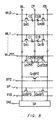
- FIG. 12 A circuit configuration of a seventh embodiment not included by the ferroelectric memory devices of the present invention is illustrated in FIG. 12, and the operation timing of the ferroelectric memory device is shown in FIG. 13.
- the memory cell portion of the ferroelectric memory device comprises two independent bit line precharge portions and has an H data bit line as the bit line precharge voltage source with an L data bit line in the floating state as in the sixth embodiment.
- the first bit line precharge portion is the same as that of the sixth embodiment.
- the bit line BL and the ground voltage VSS, the bit line /BL and the ground voltage VSS are connected by the N channel type MOS transistors QnBP0 and QnBP1, respectively.
- the gate electrodes of the N channel type MOS transistors QnBP0 and QnBP1 are connected to the bit line precharge controlling signal BP.
- the bit line BL and the ground voltage VSS, the bit line /BL and the ground voltage VSS are connected by the N channel type MOS transistors connected in series, QnBP3 and QnBP4, QnBP6 and QnBP5, respectively.
- the gate of the N channel type MOS transistor QnBP3 is connected to a signal made by amplifying the bit line BL with the sense amplifier through DL.
- the gates of the N channel type MOS transistors QnBP4, QnBP5 are connected to the bit line precharge controlling signal BP3.
- the gate of QnBP6 is connected, via /DL, to a signal made by amplifying the bit line /BL with the sense amplifier.
- the operation timing of the ferroelectric memory device will be explained with reference to the operation timing chart of FIG. 13.
- the bit line precharge controlling signals BP and BP3 are made to assume a logical voltage "H” and accordingly the bit lines BL, /BL assume a logical voltage "L” to read out the data in the memory cell.
- the word lines WL0 to WL255 and the cell plate electrode CP assume the ground voltage VSS, which is the logical voltage "L”.
- the gate controlling signal CS of the switch transistor connecting the bit lines BL, /BL and the data lines DL, /DL is made to assume the logical voltage "H" so as to connect the bit lines and the data lines. Then by changing the word line WL0 and the cell plate electrode CP to the logical voltage "H", the data in the memory cell capacitors C0, C0B are read out to the bit lines BL, /BL.
- the sense amplifier controlling signal SAE is changed to the logical voltage "H" to operate the sense amplifier SA.
- bit lines BL, /BL assume the ground voltages VSS.
- word line WL0 to be the logical voltage "L”
- the memory cell capacitors C0 and C0B are detached from the bit lines BL, /BL.
- SAE to the logical voltage "L”
- the gate of the transistor in the second bit line precharge portion since the gate of the transistor in the second bit line precharge portion is connected to the bit line, the lower the bit line potential becomes, the more difficult precharging the bit line becomes.
- the potential of the bit line since the potential of the bit line is amplified with the sense amplifier and the data are latched, a sufficient voltage is applied to the gate of the transistor of the second bit line precharge portion even when the bit line potential is low. That is, the bit line can be sufficiently precharged without suffering the effect of the threshold of the transistor.
- FIG. 14 A circuit configuration of an eighth embodiment of the ferroelectric memory devices of the present invention is illustrated in FIG. 14.
- the circuit configuration of this embodiment is similar to that of the second embodiment except that the cell plate electrodes of the memory cell capacitor comprising the complementary data are formed independently. These independent cell plate electrodes are each driven with an individual driver respectively.
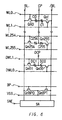
- FIG. 15 A circuit configuration of a ninth embodiment of the ferroelectric memory devices not included by the present invention is illustrated in FIG. 15.
- the circuit configuration of this embodiment is similar to that of the eighth embodiment except that the independently formed cell plate electrodes of the memory cell capacitor comprising the complementary data are arranged to the word lines direction.
- FIG. 16 A circuit configuration of a tenth embodiment of the ferroelectric memory devices of the present invention is illustrated in FIG. 16, and the operation timing of the ferroelectric memory device is shown in FIG. 17.
- the word lines are formed independent from the memory cell capacitor comprising complementary data.
- H bit lines By precharging H bit lines after turning off L bit lines, the same effect as the eighth embodiment can be achieved. That is, since the word lines of the memory cell connected to the L bit lines are turned off, the L data in the memory cell are not affected by the noise of the potential, and thus are not liable to be destroyed.
- the memory cell data are read out or written in the state in which the electric field of the memory cell capacitor is zero, an electric field stress is not applied on the capacitor and the effect of the electric field on the ferroelectric capacitor is alleviated to prolong the life of the device.
- a ferroelectric memory device with high reliability can be obtained.
Description
- The present invention relates to a ferroelectric memory device that is not liable to cause a malfunction by applying an electric field to the ferroelectric capacitor.
- A ferroelectric memory device to realize nonvolate stored data by using a ferroelectric material in the capacitor of the memory cell has been proposed. The ferroelectric capacitor has a hysteresis characteristic and thus a remanence having a different polarity remains even when the electric field is zero, according to the magnetic history. By expressing the stored data with a remanence of the ferroelectric capacitor, a nonvolatile memory device can be realized.
- Two kinds of ferroelectric memory devices are disclosed in U. S. Patent No. 4,873,664. In the first type, a main body memory cell comprises one transistor and one capacitor (1T1C) per one bit. For example, one dummy memory cell (reference cell) is comprised for a block of 256 main body memory cells (normal cells).
- In the second type, a main body memory cell comprises two transistors and two capacitors (2T2C) per one bit without having a dummy memory cell. That is, one pair of complementary data is stored in one pair of ferroelectric capacitors. The preamble of
claim 1 is based on such a 2T2C main body memory cell. - As examples of ferroelectric materials to form a capacitor, KNO3, PbLa2O3-ZrO2-TiO2 and PbTiO3-PbZrO3 are known. A ferromagnetic material having a fatigue much smaller than that of PbTiO3-PbZrO3 and thus suitable for a ferroelectric memory device is disclosed in the official gazette of the PCT international publication No. WO93/12542.
- According to the above mentioned 1T1C type ferroelectric memory device in U. S. Patent No. 4,873,664, the dummy memory cell capacitor has a capacity, namely an area, at least double that of the main body memory cell capacitor. Besides, the main body memory cell capacitor reverses polarity and returns to the original polarity state, or keeps the original polarity state without reversal according to the stored data at the time of the readout. On the other hand, the dummy memory cell capacitor maintains the original polarity state without reversal regardless of the stored data in the main body memory cell. That is, the main body memory cell capacitor applies the voltage between the electrodes in both the plus and minus polarities, whereas the dummy memory cell capacitor applies the voltage between the electrodes always in one polarity.
- The voltage applied to the cell plate electrode of the main body memory cell capacitor, the voltage applied to the cell plate electrode (dummy cell plate electrode) of the dummy memory cell capacitor, the voltage applied to the word line connected to the gate electrode of the main body memory cell transistor, and the voltage applied to the word line (dummy word line) connected to the gate electrode of the dummy memory cell transistor are all 5 V, which is equal to the power source voltage.
- In reading out the data, a voltage is applied to the word line and the cell plate electrode at the same time. Besides, regardless of stored data of the main body memory cell, after switching the voltage of the cell plate electrode of the main body memory cell capacitor off, the voltage of the word line and the dummy word line is turned off and then the bit line is precharged. Furthermore, when the voltage of the word line and the dummy word line is turned off, the voltage of the cell plate electrode of the dummy memory cell capacitor is turned off at the same time.
- Since the word line is turned off in a conventional 1T1C type ferroelectric memory device with the electric field remains in the capacitor as mentioned above, the state in which the electric field remains in the capacitor continues. As a consequence, the electric field stress is applied on the capacitor, and thus particularly under conditions of high voltage or high temperature, it provides a factor in deteriorating the capacitor. Moreover, when a potential the same as that of the cell plate is applied to the bit line in order to eliminate the residual electric field in the memory cell capacitor, the cell plate potential may become negative when the driving ability of the cell plate is small. In this case, the "L" data of the memory cell capacitor connected to the cell plate may be destroyed.
- Further, if the power source voltage is high, the electric field on the memory cell capacitor deteriorates the characteristics of the memory cell capacitor to cause a problem in that the operating margin reduces. The above mentioned are problems common to the 1T1C type and the 2T2C type.
- An object of the present invention is to alleviate the effect of the electric field applied to the ferroelectric capacitor and prevent the malfunction of the ferroelectric memory device.
- This object is achieved by
claim 1. - FIG. 1 is a diagram of the circuit configuration of a first embodiment of the ferroelectric memory devices not included by the present invention;
- FIG. 2 is a timing chart of the operation of the first embodiment of the ferroelectric memory devices not included by the present invention;
- FIG. 3 is a diagram of the circuit configuration of a second embodiment of the ferroelectric memory devices not included by the present invention;
- FIG. 4 is a timing chart of the operation of the second embodiment of the ferroelectric memory devices not included by the present invention;
- FIG. 5 is a timing chart of the operation of the third embodiment of the ferroelectric memory devices not included by the present invention;
- FIG. 6 is a diagram of the circuit configuration of a fourth embodiment of the ferroelectric memory devices not included by the present invention;
- FIG. 7 is a timing chart of the operation of the fourth embodiment of the ferroelectric memory devices not included by the present invention;
- FIG. 8 is a diagram of the circuit configuration of a fifth embodiment of the ferroelectric memory devices of the present invention;
- FIG. 9 is a timing chart of the operation of the fifth embodiment of the ferroelectric memory devices of the present invention;
- FIG. 10 is a diagram of the circuit configuration of a sixth embodiment of the ferroelectric memory devices of the present invention;
- FIG. 11 is a timing chart of the operation of the sixth embodiment of the ferroelectric memory devices of the present invention;
- FIG. 12 is a diagram of the circuit configuration of a seventh embodiment of the ferroelectric memory devices not included by the present invention;
- FIG. 13 is a timing chart of the operation of the seventh embodiment of the ferroelectric memory devices not included by the present invention;
- FIG. 14 is a diagram of the circuit configuration of a eighth embodiment of the ferroelectric memory devices of the present invention;
- FIG. 15 is a diagram of the circuit configuration not included by a ninth embodiment of the ferroelectric memory devices of the present invention;
- FIG. 16 is a diagram of the circuit configuration of a tenth embodiment of the ferroelectric memory devices of the present invention; and
- FIG. 17 is a timing chart of the operation of the tenth embodiment of the ferroelectric memory devices of the present invention.
-
- Hereinafter the present invention will be further explained with reference to embodiments and drawings.
- A circuit configuration of a first embodiment of the ferroelectric memory devices not included by the present invention is illustrated in FIG. 1. The operation timing of this ferroelectric memory device is shown in FIG. 2. The memory cell of the ferroelectric memory device stores data of one bit with one transistor and one ferroelectric capacitor.
- In FIG. 1, WL0 to WL 255 represent word lines; DWL0 and DWL1 dummy word lines; BL and /BL bit lines; CP a cell plate electrode; DCP a dummy cell plate electrode; BP a bit line precharge controlling signal; DCRST a dummy memory cell data initializing controlling signal; SAE a sense amplifier controlling signal; VSS a ground voltage; SA a sense amplifier; C0 to C255 main body memory cell capacitors; DC0 and DC1 dummy memory cell capacitors; Qn0 to Qn255, QnD0 to QnD1, QnR0 to QnR1, and QuBP0 to QnBP1 N channel type MOS transistors. Hereinafter Qn0 to Qn255 are called main body memory cell transistors and QnD0 to QnD1 are called dummy memory cell transistors.
- In FIG. 1, bit lines BL, /BL are connected to the sense amplifier SA. The sense amplifier SA is controlled by the sense amplifier controlling signal SAE. The first electrode of the dummy memory cell capacitor DC0 is connected to the bit line /BL via the dummy memory cell transistor QnD0 whose gate electrode is connected to the dummy word line DWL0, and the second electrode thereof is connected to the dummy cell plate electrode DCP.
- The first electrode of the dummy memory cell capacitor DC1 is connected to the bit line BL via the dummy memory cell transistor QnD1 whose gate electrode is connected to the word line DWL1, and the second electrode thereof is connected to the dummy cell plate electrode DCP. The first electrodes of the dummy memory cell capacitors DC0, DC1 are connected to the ground voltage VSS, which is the dummy memory cell data initializing voltage, via the N channel type MOS transistors QnR0, QnR1 to which gate electrode the dummy memory cell data initializing controlling signal DCRST is applied.
- In addition, the first electrode of the main body memory cell capacitor C0 is connected to the bit line BL via the main body memory cell transistor Qn0 whose gate electrode is connected to the word line WL0 and the second electrode thereof is connected to the cell plate electrode CP. The first electrode of the main body memory cell capacitor C1 is connected to the bit line /BL via the main body memory cell transistor Qn1 whose gate electrode is connected to the word line WL1, and the second electrode thereof is connected to the cell plate electrode CP.
- The operation timing of reading out the data stored in the main body memory cell capacitor C0 is illustrated in FIG. 2. As the initial state, the bit line precharge controlling signal BP is made to be a logical voltage "H" and accordingly the bit lines BL, /BL are made to be a logical voltage "L". Further, the word lines WL0 to WL255, the dummy word lines DWL0 to DWL1, the cell plate electrode CP, and the dummy cell plate electrode DCP are made to be the logical voltage "L". And the dummy memory cell data initializing controlling signal DCRST is made to be the logical voltage "H" to initialize the dummy memory cell capacitors DC0 and DC1.
- Then by changing the bit line precharge controlling signal BP to assume the logical voltage "L", the bit lines BL, /BL come into the floating state, and further by changing the dummy memory cell data initializing controlling signal DCRST to assume the logical voltage "L", the first electrodes of the dummy memory cell capacitors DC0 and DC1 are in the floating state.
- By changing the word line WL0, the dummy word line DWL0, the cell plate electrode CP and the dummy cell plate electrode DCP are changed to the logical voltage "H", the data in the main body memory cell capacitor C0 are read out to the bit line BL, and the data in the dummy memory cell capacitor DC0 are read out to the bit line /BL.
- The sense amplifier controlling signal SAE is changed to the logical voltage "H" to operate the sense amplifier SA. Then by changing the cell plate electrode CP to the logical voltage "L", the data of the main body memory cell capacitor C0 are rewritten. By changing the dummy word line DWL0 to assume the logical voltage "L", the dummy memory cell capacitor DC0 is detached from the bit line /BL. By changing the sense amplifier controlling signal SAE to the logical voltage "L", the operation of the sense amplifier SA is stopped. By changing the bit line precharge controlling signal BP to the logical voltage "H", the bit lines BL, /BL assume the ground voltage VSS.
- In the above mentioned conditions the state in which an electric field is not applied to the main body memory cell capacitor C0 can be achieved. Further, by changing the dummy memory cell data initializing controlling signal DCRST to the logical voltage "H", an electric field is applied to the dummy memory cell capacitor DC0 to restore the state of the dummy memory cell capacitor DC0 with certainty.
- The dummy cell plate electrode DCP is changed to the logical voltage "L" to make the electric field applied on the dummy memory cell capacitor DC0 zero. Further, by changing the word line WL0 to be the logical voltage "L", the main body memory cell capacitor C0 is detached from the bit lines BL, /BL. With this operation, reading out and rewriting of the data can be finished in the state in which an electric field is not applied to the main body memory cell capacitor C0 and the dummy memory cell capacitor DC0. The circuit configuration and the operation timing described herein represent just one example, and thus it is sufficient if only the electric field on the memory cell capacitor satisfies the above mentioned relationship.
- Features of the ferroelectric memory device of this embodiment include that rewriting of the data is finished in the state in which a load does not remain nor is an electric field applied on the memory cell capacitor. If the word line is changed to be the logical voltage "L" before precharging the bit line to the ground voltage VSS, a load remains in the memory cell capacitor and thus an electric field continues to be on the memory cell capacitor until the load is eliminated by leakage or some other reason. In this case, the memory cell capacitor may deteriorate.
- For example, in a device which operates in a 200 x 10-9 second cycle and with the time duration in which an electric field is on the memory cell capacitor for 20 x 10-9 seconds, then the time in which an electric field is applied on the memory cell capacitor is 1/10 of the cycle and so the life of the capacitor can extend to 10 times. The longer the operation cycle is, the longer the life of the capacitor becomes. Furthermore, in a conventional operation in which a load remains on the device, the life is determined by the entire operation time regardless of the cycle time.
- In the first embodiment, the ferroelectric memory cell stores data of one bit with one transistor and one ferroelectric capacitor. On the other hand, the ferroelectric memory cell of a second embodiment stores data of one bit with two transistors and two ferroelectric capacitors so that complementary data are stored in ferroelectric capacitors respectively. A circuit configuration of the second embodiment of the ferroelectric memory devices of the present invention is illustrated in FIG. 3. The operation timing of this ferroelectric memory device is shown in FIG. 4.
- In FIG. 3, WL0 to WL 255 represent word lines; BL and /BL bit lines; CP a cell plate electrode; BP a bit line precharge controlling signal; SAE a sense amplifier controlling signal; VSS a ground voltage; SA a sense amplifier; C0 to C255, C0B to C255B memory cell capacitors; Qn0 to Qn255, Qn0B to Qn255B, QnBP0 to QnBP2 N channel type MOS transistors.
- In FIG. 3, bit lines BL, /BL are connected to the sense amplifier SA. The sense amplifier SA is controlled by the sense amplifier controlling signal SAE. The first electrode of the memory cell capacitor C0 is connected to the bit line BL via the memory cell transistor Qn0 whose gate electrode is connected to the word line WL0, and the second electrode thereof is connected to the cell plate electrode CP. And the first electrode of the memory cell capacitor C0B, which is the companion to the memory cell capacitor C0, is connected to the bit line /BL via the memory cell transistor Qn0B whose gate electrode is connected to the word line WL0, and the second electrode thereof is connected to the cell plate electrode CP.
- The connections of the other memory cell capacitors C1 to C255 and C1B to C255B are the same as the above mentioned memory cell capacitors C0 and C0B. The bit lines BL, /BL are connected by the N channel type MOS transistor QnBP2. The bit line BL and the ground voltage VSS, and the bit line /BL and the ground voltage VSS are connected by the N channel type MOS transistors QnBP0, QnBP2 respectively. The gate electrodes of the N channel type MOS transistors QnBP0 to QnBP1 are connected to the bit line precharge controlling signal BP.
- The operation timing of the ferroelectric memory device will be explained with reference to the operation timing chart of FIG. 4. The bit line precharge controlling signal BP is made to assume a logical voltage "H" and accordingly the bit lines BL, /BL assume a logical voltage "L" to read out the data in the memory cell. The word lines WL0 to WL255 and the cell plate electrode CP assume the ground voltage VSS, which is the logical voltage "L".
- Then by changing the bit line precharge controlling signal BP to assume the logical voltage "L", the bit lines BL, /BL come into the floating state, and further by changing the word line WL0 and the cell plate electrode CP to the logical voltage "H", the data in the main body memory cell capacitors C0, C0B are read out to the bit lines BL, /BL. The sense amplifier controlling signal SAE is changed to the logical voltage "H" to operate the sense amplifier SA. Then by changing the cell plate electrode CP to the logical voltage "L", the data of the memory cell capacitors C0 and C0B are rewritten.
- By changing the word line WL0 to assume the logical voltage "L", the memory cell capacitors C0 and C0B are detatched from the bit lines BL, /BL. With this operation, reading out and rewriting the data can be finished in the state in which an electric field is not applied on the main body memory cell capacitors C0 and C0B. The circuit configuration and the operation timing described herein represents just one example, and thus it is sufficient if only the electric field on the memory cell capacitor satisfies the above mentioned relationship.
- Features of the ferroelectric memory device of this embodiment include that rewriting of the data is finished in the state in which a load does not remain nor is an electric field applied on the memory cell capacitors as in the first embodiment. That is, by shortening the time during which an electric field is applied on the memory cell capacitors, the deterioration of the memory cell capacitor can be prevented to prolong its life.
- In the above mentioned second embodiment, the state in which a load does not remain in the memory cell capacitor was achieved after rewriting, whereas in the third embodiment, the state can be realized before initiating reading out as well. As in the second embodiment, the ferroelectric memory device of the third embodiment stores data of one bit with two transistors and two ferroelectric capacitors. A configuration like the first embodiment in that the ferroelectric memory device stores data of one bit with one transistor and one ferroelectric capacitor can be employed as well. Since the circuit configuration of the ferroelectric memory device is the same as that of the second embodiment illustrated in FIG. 3, details of the circuit are not described herein.
- The operation timing of the ferroelectric memory device will be explained with reference to the operation timing chart of FIG. 5. The bit line precharge controlling signal BP is made to assume a logical voltage "H" and accordingly the bit lines BL, /BL assume a logical voltage "L" to read out the data in the memory cell. The word lines WL0 to WL255, the cell plate electrode CP assume the ground voltage VSS, which is the logical voltage "L".
- Then by changing the word line WL0 to the logical voltage "H", the memory cell capacitors and the bit lines are connected. At the time, since the bit line precharge controlling signal BP is still a logical voltage "H" and the voltage of the both electrodes of the memory cell capacitors is the ground voltage VSS, an electric field is not applied. Then, by changing the bit line precharge controlling signal BP to assume the logical voltage "L", the bit lines BL, /BL come into the floating state.
- Then by changing the cell plate electrode CP to the logical voltage "H", the data of the memory cell capacitors C0 and C0B are read out to the bit lines BL and /BL. The sense amplifier controlling signal SAE is changed to the logical voltage "H" to operate the sense amplifier SA. Then by changing the cell plate electrode CP to the logical voltage "L", the data of the memory cell capacitors C0 and C0B are rewritten.
- By changing the sense amplifier controlling signal SAE to assume the logical voltage "L", the operation of the sense amplifier SA is stopped. Then by changing the bit line precharge controlling signal BP to the logical voltage "H", the bit lines BL, /BL assume the ground voltage VSS. The state in which an electric field is not applied to the memory cell capacitors C0 and C0B can be realized. By changing the word line WL0 to the logical voltage "L", the memory cell capacitors C0 and C0B are detached from the bit lines BL, /BL. With this operation, reading out and rewriting the data can be finished in the state in which an electric field is not applied on the memory cell capacitors C0 and C0B.
- Features of the ferroelectric memory device of this embodiment include that rewriting of the data is finished in the state in which a load does not remain nor is an electric field applied on the memory cell capacitors as in the second embodiment. And further, since the electric field across the electrodes of the memory cell capacitor is zero before reading out the data, the voltage in the electrode in the floating state, which is opposite to the cell plate electrode can be reset. Thus, the data can be read out stably.
- A circuit configuration of a fourth embodiment of the ferroelectric memory devices not included by the present invention is illustrated in FIG. 6. The operation timing of the ferroelectric memory device is shown in FIG. 7. The memory cell of the ferroelectric memory device stores data of one bit with one transistor and one ferroelectric capacitor.
- In FIG. 6, WL0 to WL 255 represent word lines; DWL0 to DWL1 dummy word lines; BL and /BL bit lines; CP a cell plate electrode; DCP a dummy cell plate electrode; BP a bit line precharge controlling signal; SAE a sense amplifier controlling signal; VSS a ground voltage; SA a sense amplifier; C0 to C255 main body memory cell capacitors; DC0 to DC1 dummy memory cell capacitors; Qn0 to Qn255, QnD0 to QnD1, and QnBP0 to QnBP1 N channel type MOS transistors. Hereinafter Qn0 to Qn255 are called main body memory cell transistors and QnD0 to QnD1 are called dummy memory cell transistors.
- In FIG. 6, bit lines BL, /BL are connected to the sense amplifier SA. The sense amplifier SA is controlled by the sense amplifier controlling signal SAE. The first electrode of the dummy memory cell capacitor DC0 is connected to the bit line /BL via the dummy memory cell transistor QnD0 whose gate electrode is connected to the dummy word line DWL0. The second electrode of DC0 is connected to the dummy cell plate electrode DCP. The first electrode of the dummy memory cell capacitor DC1 is connected to the bit line BL via the dummy memory cell transistor QnD1 whose gate electrode is connected to the word line DWL1. The second electrode of DC1 is connected to the dummy cell plate electrode DCP.
- In addition, the first electrode of the main body memory cell capacitor C0 is connected to the bit line BL via the main body memory cell transistor Qn0 whose gate electrode is connected to the word line WL0. The second electrode of C0 is connected to the cell plate electrode CP. The first electrode of the main body memory cell capacitor C1 is connected to the bit line /BL via the main body memory cell transistor Qn1 whose gate electrode is connected to the word line WL1. The second electrode of C1 is connected to the cell plate electrode CP.
- The operation timing of reading out the data stored in the main body memory cell capacitor C0 is illustrated in FIG. 7. As the initial state, the bit line precharge controlling signal BP is made to assume a logical voltage "H" and accordingly the bit lines BL, /BL assume a logical voltage "L". Further, the word lines WL0 to WL255, the dummy word lines DWL0 to DWL1, the cell plate electrode CP, and the dummy cell plate electrode DCP assume the logical voltage "L".
- By changing the bit line precharge controlling signal BP to be the logical voltage "L", the bit lines BL, /BL come into the floating state. By changing the word line WL0, the dummy word line DWL0, the cell plate electrode CP and the dummy cell plate electrode DCP are changed to the logical voltage "H", the data in the main body memory cell capacitor C0 are read out to the bit line BL, and the data in the dummy memory cell capacitor DC0 are read out to the bit line /BL.
- The sense amplifier controlling signal SAE is changed to the logical voltage "H" to operate the sense amplifier SA. Then by changing the cell plate electrode CP to the logical voltage "L", the data of the main body memory cell capacitor C0 are rewritten. By changing the sense amplifier controlling signal SAE to the logical voltage "L", the operation of the sense amplifier SA is stopped. By changing the bit line precharge controlling signal BP to the logical voltage "H", the bit lines BL, /BL are made to assume the ground voltages VSS. In the above mentioned conditions the state in which an electric field is not applied to the main body memory cell capacitor C0 can be achieved.
- The dummy cell plate electrode DCP is changed to the logical voltage "L" to make the electric field applied to the dummy memory cell capacitor DC0 zero. Further, by changing the word line WL0 and the dummy word line DWL0 to the logical voltage "L", the main body memory cell capacitor C0 and the dummy memory cell capacitor DC0 are detatched from the bit line /BL. With this operation, reading out and rewriting the data can be finished in the state in which an electric field is not applied on the main body memory cell capacitor C0 and the dummy memory cell capacitor DC0.
- The circuit configuration and the operation timing described herein represents just one example, and thus it is sufficient if only the electric field on the memory cell capacitor satisfies the above mentioned relationship. Further, a configuration in combination with the above mentioned third embodiment to realize the state in which an electric field is not applied on the both electrodes of the memory cell capacitors before reading out the information can be employed as well.
- Features of the ferroelectric memory device of this embodiment include that rewriting of the data is finished in the state in which a load does not remain nor an electric field is applied on the memory cell capacitor as in the first embodiment. However, although a controlling signal to initialize the dummy memory cell data and an N channel type MOS transistor are necessary in the first embodiment, a circuit element for initializing the dummy memory cell data is unnecessary in this embodiment.
- A circuit configuration of a fifth embodiment of the ferroelectric memory devices of the present invention is illustrated in FIG. 8, and the operation timing of the ferroelectric memory device is shown in FIG. 9. The memory cell of the ferroelectric memory device includes independent bit line precharge (BP) and bit line equalize (BP2) portions.
- In FIG. 8, bit lines BL, /BL are connected to the sense amplifier SA. The sense amplifier SA is controlled by the sense amplifier controlling signal SAE. The first electrode of the memory cell capacitor C0 is connected to the bit line BL via the memory cell transistor Qn0 whose gate electrode is connected to the word line WL0. The second electrode of C0 is connected to the cell plate electrode CP.
- The first electrode of the memory cell capacitor C0B, which is the companion to the memory cell capacitor C0, is connected to the bit line /BL via the memory cell transistor Qn0B whose gate electrode is connected to the word line WL0. The second electrode of C0B is connected to the cell plate electrode CP. The connections of the other memory cell capacitors C1 to C255 and C1B to C255B are the same as the above mentioned memory cell capacitors C0 and C0B.
- The bit lines BL, /BL are connected with the N channel type MOS transistor QnBP2. The bit line BL and the ground voltage VSS, and the bit line /BL and the ground voltage VSS are connected with the N channel type MOS transistors QnBP0, QnBP1 respectively. The gate electrodes of the N channel type MOS transistors QnBP0 and QnBP1 are connected to the bit line precharge controlling signal BP, and the gate electrode of the N channel type MOS transistor QnBP2 is connected to the bit line equalize controlling signal BP2.
- The operation timing of the ferroelectric memory device will be explained with reference to the operation timing chart of FIG. 9. The bit line precharge controlling signal BP and bit line equalizing control signal BP2 are made to assume logical voltage "H" and accordingly the bit lines BL, /BL assume a logical voltage "L" to read out the data in the memory cell. The word lines WL0 to WL255 and the cell plate electrode CP are made to assume the ground voltage VSS, which is the logical voltage "L". Then by changing the bit line precharge controlling signals BP, BP2 to be the logical voltage "L", the bit lines BL, /BL come into the floating state.
- Then by changing the word line WL0 and the cell plate electrode CP to the logical voltage "H", the data in the memory cell capacitors C0, C0B are read out to the bit lines BL, /BL. The sense amplifier controlling signal SAE is changed to the logical voltage "H" to operate the sense amplifier SA. Then by changing the cell plate electrode CP to the logical voltage "L", the data of the memory cell capacitors C0 and C0B are rewritten. By changing the sense amplifier controlling signal SAE to the logical voltage "L", the operation of the sense amplifier SA is then stopped.
- By changing the bit line controlling signal BP to the logical voltage "H", the bit lines BL, /BL are made to be the ground voltages VSS. In the above mentioned conditions the state in which an electric field is not applied to the main body memory cell capacitors C0 and C0B can be achieved. Then by changing the word line WL0 to the logical voltage "L", the memory cell capacitors C0 and C0B are detached from the bit lines BL, /BL. With this operation, reading out and rewriting the data can be finished in the state in which an electric field is not applied on the main body memory cell capacitors C0 and C0B.
- Further, by changing the bit line controlling signal BP2 to the logical voltage "H", the bit lines BL, /BL are equalized. While the risk of a rise in the potential in the bit line, which should be L at the time of equalizing the bit lines BL, /BL, exists to result in destruction of the L data if the bit line precharge signal and the bit line equalize signal are the same, as in the second embodiment, then the risk of destroying the L data may be reduced with this embodiment.
- The circuit configuration and the operation timing described herein represents just one example, and thus it is sufficient if only the electric field on the memory cell capacitor satisfies the above mentioned relationship.
- A circuit configuration of a sixth embodiment of the ferroelectric memory devices of the present invention is illustrated in FIG. 10. And the operation timing of the ferroelectric memory device is shown in FIG. 11. The memory cell of the ferroelectric memory device comprises two independent bit line precharge portions and has an H data bit line as the bit line precharge voltage source with an L data bit line in the floating state as in the first and fifth embodiments.
- In FIG. 10, the first bit line precharge portion is the same as that of the fifth embodiment. The bit line BL and the ground voltage VSS, the bit line /BL and the ground voltage VSS are connected by the N channel type MOS transistors QnBP0, QnBP1 respectively. The gate electrodes of the N channel type MOS transistors QnBP0 to QnBP1 are connected to the bit line precharge controlling signal BP.
- In the second bit line precharge portion, the bit line BL and the ground voltage VSS, and the bit line /BL and the ground voltage VSS are connected with the N channel type MOS transistors connected in series, QnBP3 and QnBP4, QnBP6 and QnBP5, respectively. The gate of the N channel type MOS transistor QnBP3 is connected to the bit line BL. The gate of the N channel type MOS transistor QnBP6 is connected to the bit line /BL. The gate electrodes of the N channel type MOS transistors QnBP4, QnBP5 are connected to the bit line precharge controlling signal BP3.
- The operation timing of the ferroelectric memory device will be explained with reference to the operation timing chart of FIG. 11. The bit line precharge controlling signal BP is made to assume a logical voltage "H" and accordingly the bit lines BL, /BL assume a logical voltage "L" to read out the data in the memory cell. The word lines WL0 to WL255, and the cell plate electrode CP assume the ground voltage VSS, which is the logical voltage "L". Then by changing the bit line precharge controlling signals BP, amd BP3 to be the logical voltage "L", the bit lines BL, /BL come into the floating state.
- By changing the word line WL0 and the cell plate electrode CP to the logical voltage "H", the data in the memory cell capacitors C0, C0B are read out to the bit lines BL, /BL. The sense amplifier controlling signal SAE is changed to the logical voltage "H" to operate the sense amplifier SA. Then by changing the cell plate electrode CP to the logical voltage "L", the data of the memory cell capacitors C0 and C0B are rewritten.
- By changing the sense amplifier controlling signal SAE to the logical voltage "L", the operation of the sense amplifier SA is stopped. By changing the bit line controlling signal BP3 to the logical voltage "H", only the H bit lines assume the ground voltage VSS and L bit lines come into the floating state. In the above mentioned conditions the state in which an electric field is not applied to the memory cell capacitors C0 and C0B can be achieved.
- By changing the bit line controlling signal BP to the logical voltage "H", the bit lines BL, /BL are made to assume the ground voltages VSS. Then by changing the word line WL0 to the logical voltage "L", the memory cell capacitors C0 and C0B are detached from the bit lines BL, /BL. With this operation, reading out and rewriting the data can be finished in the state in which an electric field is not applied on the main body memory cell capacitors C0 and C0B.
- In this embodiment, since H data bit lines are precharged after having L data bit lines in the floating state, the potential of the electrode opposite to the memory cell plate of the L data memory cell changes according to the change of the potential of the cell plate caused by noise. Therefore, since the electric field is so small, the risk of L data destruction is reduced.
- A circuit configuration of a seventh embodiment not included by the ferroelectric memory devices of the present invention is illustrated in FIG. 12, and the operation timing of the ferroelectric memory device is shown in FIG. 13. The memory cell portion of the ferroelectric memory device comprises two independent bit line precharge portions and has an H data bit line as the bit line precharge voltage source with an L data bit line in the floating state as in the sixth embodiment.
- In FIG. 12, the first bit line precharge portion is the same as that of the sixth embodiment. The bit line BL and the ground voltage VSS, the bit line /BL and the ground voltage VSS are connected by the N channel type MOS transistors QnBP0 and QnBP1, respectively. The gate electrodes of the N channel type MOS transistors QnBP0 and QnBP1 are connected to the bit line precharge controlling signal BP.
- In the second bit line precharge portion, the bit line BL and the ground voltage VSS, the bit line /BL and the ground voltage VSS are connected by the N channel type MOS transistors connected in series, QnBP3 and QnBP4, QnBP6 and QnBP5, respectively. The gate of the N channel type MOS transistor QnBP3 is connected to a signal made by amplifying the bit line BL with the sense amplifier through DL. The gates of the N channel type MOS transistors QnBP4, QnBP5 are connected to the bit line precharge controlling signal BP3. The gate of QnBP6 is connected, via /DL, to a signal made by amplifying the bit line /BL with the sense amplifier.
- The operation timing of the ferroelectric memory device will be explained with reference to the operation timing chart of FIG. 13. The bit line precharge controlling signals BP and BP3 are made to assume a logical voltage "H" and accordingly the bit lines BL, /BL assume a logical voltage "L" to read out the data in the memory cell. The word lines WL0 to WL255 and the cell plate electrode CP assume the ground voltage VSS, which is the logical voltage "L". By changing the bit line precharge controlling signals BP and BP3 to be the logical voltage "L", the bit lines BL, /BL come into the floating state.
- The gate controlling signal CS of the switch transistor connecting the bit lines BL, /BL and the data lines DL, /DL is made to assume the logical voltage "H" so as to connect the bit lines and the data lines. Then by changing the word line WL0 and the cell plate electrode CP to the logical voltage "H", the data in the memory cell capacitors C0, C0B are read out to the bit lines BL, /BL. The sense amplifier controlling signal SAE is changed to the logical voltage "H" to operate the sense amplifier SA.
- Then by changing the cell plate electrode CP to the logical voltage "L", the data of the memory cell capacitors C0 and C0B are rewritten. By changing the controlling signal CS to the logical voltage "L", the sense amplifier SA is detatched from the bit line. By changing the bit line controlling signal BP3 to the logical voltage "H", only the H bit lines assume the ground voltages VSS and L bit lines come into the floating state. In the above mentioned conditions the state in which an electric field is not applied to the memory cell capacitors C0 and C0B can be achieved.
- By changing the bit line controlling signal BP to the logical voltage "H", the bit lines BL, /BL assume the ground voltages VSS. Then by changing the word line WL0 to be the logical voltage "L", the memory cell capacitors C0 and C0B are detached from the bit lines BL, /BL. With this operation, reading out and rewriting the data can be finished in the state in which an electric field is not applied on the main body memory cell capacitors C0 and C0B. Finally, by changing the sense amplifier controlling signal SAE to the logical voltage "L", the operation of the sense amplifier SA is stopped.
- In the above mentioned sixth embodiment, since the gate of the transistor in the second bit line precharge portion is connected to the bit line, the lower the bit line potential becomes, the more difficult precharging the bit line becomes. On the other hand, in this embodiment, since the potential of the bit line is amplified with the sense amplifier and the data are latched, a sufficient voltage is applied to the gate of the transistor of the second bit line precharge portion even when the bit line potential is low. That is, the bit line can be sufficiently precharged without suffering the effect of the threshold of the transistor.
- A circuit configuration of an eighth embodiment of the ferroelectric memory devices of the present invention is illustrated in FIG. 14. The circuit configuration of this embodiment is similar to that of the second embodiment except that the cell plate electrodes of the memory cell capacitor comprising the complementary data are formed independently. These independent cell plate electrodes are each driven with an individual driver respectively.
- In this circuit configuration, since the cell plate electrodes do not effect each other, the risk of destroying the L data connected to the L bit lines is reduced in the operation of having the H bit line become L and the electric field zero.
- A circuit configuration of a ninth embodiment of the ferroelectric memory devices not included by the present invention is illustrated in FIG. 15. The circuit configuration of this embodiment is similar to that of the eighth embodiment except that the independently formed cell plate electrodes of the memory cell capacitor comprising the complementary data are arranged to the word lines direction.
- In this circuit configuration, since the cell plate electrodes do not effect each other, the risk of destroying the L data connected to the L bit lines is reduced in the operation of having the H bit line become L and the electric field zero. Concerning this effect, the smaller the number of selected memory cells connected to one cell plate electrode is, the greater the effect can be.
- A circuit configuration of a tenth embodiment of the ferroelectric memory devices of the present invention is illustrated in FIG. 16, and the operation timing of the ferroelectric memory device is shown in FIG. 17. In the ferroelectric memory device of this embodiment, the word lines are formed independent from the memory cell capacitor comprising complementary data. By precharging H bit lines after turning off L bit lines, the same effect as the eighth embodiment can be achieved. That is, since the word lines of the memory cell connected to the L bit lines are turned off, the L data in the memory cell are not affected by the noise of the potential, and thus are not liable to be destroyed.
- As heretofore mentioned, according to the present invention, since the memory cell data are read out or written in the state in which the electric field of the memory cell capacitor is zero, an electric field stress is not applied on the capacitor and the effect of the electric field on the ferroelectric capacitor is alleviated to prolong the life of the device. Thus a ferroelectric memory device with high reliability can be obtained.
Claims (5)
- A ferroelectric memory device comprising first and second bit lines (BL, /BL), a main body memory cell conprising a first ferroelectric capacitor (C0) and a first memory cell transistor (Qn0) serially connected between said first bit line and a cell plate eine (CP), and a second ferroelectric capacitor (C0B) and a second memory cell transistor (Qn0B) serially connected between said second bit line and said cell plate eine, characterized in that
the device further comprises a first reset circuit (QnBP3 - QnBP6) connected to the first and second bit lines and a second reset circuit (QnBP0, QnBP1) connected to the first and second bit lines, and
when after applying predetermined electric fields to the first and second ferroelectric capacitors, the electric fields are made zero, either of the first and second ferroelectric capacitors to which the electric field has been applied is brought, by the first reset circuit, to a state that no electric field is applied, and then both of the first and second ferroelectric capacitors are brought, by the second reset circuit, to a state that no electric field is applied (fig. 10). - A ferroelectric memory device according to claim 1,
wherein the first reset circuit comprises third and fourth transistors (QnBP0, QnBP1) of which gate signals are a first controlling signal (BP) and a bit line precharge voltage source (VSS) connected to the first and second bit lines (BL, /BL) via the third and fourth transistors respectively, and the second reset circuit comprises a fifth transistor (QnBP2) connecting the first and second bit line, a gate signal of the fifth transistor being a second controlling signal (BP2), and
wherein when the electric fields applied to the first and second ferroelectric capacitors are made zero via the first and second bit lines respectively, the first and second bit lines are connected to the bit line precharge voltage source by the first reset circuit with the first controlling signal, and then the first and second bit lines are connected to each other by the second reset circuit with the second controlling signal so as to be equalized (fig. 8). - A ferroelectric memory device according to claim 1,
wherein the first reset circuit comprises a circuit (QnBP3, QnBP4) for connecting the first bit line (BL) to a bit line precharge voltage source (VSS), and a circuit (QnBP5, QnBP6) for connecting the second bit line (/BL) to the bit line precharge voltage source with application of a bit line controlling signal BP3, and the second reset circuit comprises third and fourth transistors (QnBP0, QnBP1) of which gate signals are a first controlling signal (BP) and a bit line precharge voltage source (VSS) connected to the first and second bit lines (BL, /BL) via the third and fourth transistors respectively, and
wherein when the electric fields applied to the first and second ferroelectric capacitors are made zero via the first and second bit lines respectively, either of the first and second bit lines which has a logical voltage "L" is brought to the floating state and the other bit line which has a logical voltage "H" is connected to the bit line precharge voltage source by the first reset circuit, and then the first and second bit lines are connected to the bit line precharge voltage source by the second reset circuit with the first controlling signal (fig. 10). - A ferroelectric memory device according to claim 1,
wherein the first reset circuit comprises a first cell plate (CP1) electrode connected to the first ferroelectric capacitor (C0) and a second cell plate electrode (CP3) connected to the second ferroelectric capacitor (C0B), and the second reset circuit comprises third and fourth transistors (QnBP0, QnBP1) of which gate signals are a first controlling signal (BP) and a bit line precharge voltage source (VSS) connected to the first and second bit lines (BL, /BL) via the third and fourth transistors respectively, and
wherein when the electric fields applied to the first and second ferroelectric capacitors are made zero via the first and second bit lines respectively, the first and second cell plate electrodes are controlled separately, and then the first and second bit lines are connected to the bit line precharge voltage source by the second reset circuit with the first controlling signal (fig. 14) - A ferroelectric memory device according to claim 1,
wherein the first reset circuit comprises a first word line (WL0B) connected to a gate of the first memory cell transistor (Qn0B) and a second word line (WL0A) connected to a gate of the second memory cell transistor (Qn0), and the second reset circuit comprises third and fourth transistors (QnBP1, QnBP0) of which gate signals are a first controlling signal (BP) and a bit line precharge voltage source (VSS) connected to the first and second bit lines (/BL, BL) via the third and fourth transistors respectively, and
wherein when the electric fields applied to the first and second ferroelectric capacitors are made zero via the first and second bit lines respectively, after both the first and second memory cell transistors are turned on followed by that the first bit line becomes on the L level and the second bit line becomes on the H level, the first memory cell transistor is turned off, then the second bit line is changed from the H level to the L level, and then the first and second bit lines are connected to the bit line precharge voltage source by the second reset circuit with the first controlling signal. (fig. 16).
Applications Claiming Priority (3)
| Application Number | Priority Date | Filing Date | Title |
|---|---|---|---|
| JP19735195 | 1995-08-02 | ||
| JP19735195 | 1995-08-02 | ||
| EP96112463A EP0757354B1 (en) | 1995-08-02 | 1996-08-01 | Ferroelectric memory device |
Related Parent Applications (1)
| Application Number | Title | Priority Date | Filing Date |
|---|---|---|---|
| EP96112463A Division EP0757354B1 (en) | 1995-08-02 | 1996-08-01 | Ferroelectric memory device |
Publications (2)
| Publication Number | Publication Date |
|---|---|
| EP1069573A1 EP1069573A1 (en) | 2001-01-17 |
| EP1069573B1 true EP1069573B1 (en) | 2003-04-23 |
Family
ID=16373046
Family Applications (2)
| Application Number | Title | Priority Date | Filing Date |
|---|---|---|---|
| EP96112463A Expired - Lifetime EP0757354B1 (en) | 1995-08-02 | 1996-08-01 | Ferroelectric memory device |
| EP00118131A Expired - Lifetime EP1069573B1 (en) | 1995-08-02 | 1996-08-01 | Ferroelectric memory device with reset circuit |
Family Applications Before (1)
| Application Number | Title | Priority Date | Filing Date |
|---|---|---|---|
| EP96112463A Expired - Lifetime EP0757354B1 (en) | 1995-08-02 | 1996-08-01 | Ferroelectric memory device |
Country Status (5)
| Country | Link |
|---|---|
| US (1) | US5675530A (en) |
| EP (2) | EP0757354B1 (en) |
| KR (1) | KR100243883B1 (en) |
| DE (2) | DE69627724T2 (en) |
| SG (1) | SG64943A1 (en) |
Families Citing this family (19)
| Publication number | Priority date | Publication date | Assignee | Title |
|---|---|---|---|---|
| JP3230435B2 (en) * | 1996-05-17 | 2001-11-19 | 日本電気株式会社 | Semiconductor storage device |
| US6097624A (en) * | 1997-09-17 | 2000-08-01 | Samsung Electronics Co., Ltd. | Methods of operating ferroelectric memory devices having reconfigurable bit lines |
| KR100224673B1 (en) * | 1996-12-13 | 1999-10-15 | 윤종용 | Non-volatile ferroelectric memory device and driving method thereof |
| KR100219519B1 (en) * | 1997-01-10 | 1999-09-01 | 윤종용 | A semiconductor device having ferroelectric floating gate ram and fabrication method of the same |
| KR100297874B1 (en) | 1997-09-08 | 2001-10-24 | 윤종용 | Ferroelectric random access memory device |
| KR100282045B1 (en) * | 1998-08-07 | 2001-03-02 | 윤종용 | Nonvolatile Dynamic Random Access Memory with Ferroelectric Capacitors |
| DE19952311B4 (en) * | 1999-10-29 | 2006-07-13 | Infineon Technologies Ag | Integrated memory with memory cells of 2-transistor / 2-capacitor type |
| US6809949B2 (en) | 2002-05-06 | 2004-10-26 | Symetrix Corporation | Ferroelectric memory |
| US6906945B2 (en) * | 2003-11-18 | 2005-06-14 | Texas Instruments Incorporated | Bitline precharge timing scheme to improve signal margin |
| JP2005190565A (en) * | 2003-12-25 | 2005-07-14 | Seiko Epson Corp | Ferroelectric memory device, electronic equipment and driving method |
| JP4477629B2 (en) * | 2004-03-24 | 2010-06-09 | 富士通マイクロエレクトロニクス株式会社 | Ferroelectric memory |
| KR100673901B1 (en) * | 2005-01-28 | 2007-01-25 | 주식회사 하이닉스반도체 | Semiconductor device for low voltage |
| KR101064377B1 (en) | 2009-05-28 | 2011-09-14 | 한양대학교 산학협력단 | Non-Volatile Memory of having Cell comprising Diode |
| US9361972B1 (en) * | 2015-03-20 | 2016-06-07 | Intel Corporation | Charge level maintenance in a memory |
| WO2018044485A1 (en) | 2016-08-31 | 2018-03-08 | Micron Technology, Inc. | Ferroelectric memory cells |
| CN109643570B (en) | 2016-08-31 | 2023-11-21 | 美光科技公司 | Apparatus and method for operating ferroelectric memory including ferroelectric memory |
| KR102188490B1 (en) | 2016-08-31 | 2020-12-09 | 마이크론 테크놀로지, 인크. | Apparatus and method for accessing ferroelectric memory including ferroelectric memory |
| WO2018044510A1 (en) | 2016-08-31 | 2018-03-08 | Micron Technology, Inc. | Apparatuses and methods including two transistor-one capacitor memory and for accessing same |
| US10867675B2 (en) | 2017-07-13 | 2020-12-15 | Micron Technology, Inc. | Apparatuses and methods for memory including ferroelectric memory cells and dielectric memory cells |
Family Cites Families (10)
| Publication number | Priority date | Publication date | Assignee | Title |
|---|---|---|---|---|
| US3932848A (en) * | 1975-01-20 | 1976-01-13 | Intel Corporation | Feedback circuit for allowing rapid charging and discharging of a sense node in a static memory |
| US4873664A (en) * | 1987-02-12 | 1989-10-10 | Ramtron Corporation | Self restoring ferroelectric memory |
| CA1340340C (en) * | 1987-06-02 | 1999-01-26 | Joseph T. Evans, Jr. | Non-volatile memory circuit using ferroelectric capacitor storage element |
| JPH0713877B2 (en) * | 1988-10-19 | 1995-02-15 | 株式会社東芝 | Semiconductor memory |
| JP3169599B2 (en) * | 1990-08-03 | 2001-05-28 | 株式会社日立製作所 | Semiconductor device, driving method thereof, and reading method thereof |
| EP0616726B1 (en) * | 1991-12-13 | 2001-06-06 | Symetrix Corporation | Layered superlattice material applications |
| JP2930168B2 (en) * | 1992-10-09 | 1999-08-03 | シャープ株式会社 | Driving method of ferroelectric memory device |
| KR970000870B1 (en) * | 1992-12-02 | 1997-01-20 | 마쯔시다덴기산교 가부시기가이샤 | Semiconductor memory device |
| US5430671A (en) * | 1993-04-09 | 1995-07-04 | Matsushita Electric Industrial Co., Ltd. | Semiconductor memory device |
| JP3278981B2 (en) * | 1993-06-23 | 2002-04-30 | 株式会社日立製作所 | Semiconductor memory |
-
1996
- 1996-08-01 DE DE69627724T patent/DE69627724T2/en not_active Expired - Fee Related
- 1996-08-01 EP EP96112463A patent/EP0757354B1/en not_active Expired - Lifetime
- 1996-08-01 KR KR1019960032197A patent/KR100243883B1/en not_active IP Right Cessation
- 1996-08-01 DE DE69621293T patent/DE69621293T2/en not_active Expired - Fee Related
- 1996-08-01 US US08/691,134 patent/US5675530A/en not_active Expired - Lifetime
- 1996-08-01 EP EP00118131A patent/EP1069573B1/en not_active Expired - Lifetime
- 1996-08-02 SG SG1996010411A patent/SG64943A1/en unknown
Also Published As
| Publication number | Publication date |
|---|---|
| DE69627724T2 (en) | 2003-10-23 |
| DE69621293D1 (en) | 2002-06-27 |
| KR970012696A (en) | 1997-03-29 |
| DE69621293T2 (en) | 2002-12-12 |
| EP0757354A2 (en) | 1997-02-05 |
| DE69627724D1 (en) | 2003-05-28 |
| KR100243883B1 (en) | 2000-02-01 |
| EP0757354A3 (en) | 1998-11-04 |
| EP1069573A1 (en) | 2001-01-17 |
| SG64943A1 (en) | 1999-05-25 |
| EP0757354B1 (en) | 2002-05-22 |
| US5675530A (en) | 1997-10-07 |
Similar Documents
| Publication | Publication Date | Title |
|---|---|---|
| EP1069573B1 (en) | Ferroelectric memory device with reset circuit | |
| EP0278167B1 (en) | Self restoring ferroelectric memory | |
| KR0172017B1 (en) | Optimum signal decision apparatus for digital signal receiver | |
| US5373463A (en) | Ferroelectric nonvolatile random access memory having drive line segments | |
| US5835400A (en) | Ferroelectric memory devices having nondestructive read capability and methods of operating same | |
| JP2576425B2 (en) | Ferroelectric memory device | |
| US5969979A (en) | Ferroelectric memory device | |
| US5517446A (en) | Nonvolatile semiconductor memory device and method for driving the same | |
| US5991188A (en) | Non-volatile ferroelectric memory with section plate line drivers and method for accessing the same | |
| JPH0734315B2 (en) | NONVOLATILE MEMORY CELL AND READING METHOD THEREOF | |
| WO1995002883A1 (en) | Non-volatile memory | |
| US6912149B2 (en) | Ferroelectric memory device and method for reading data from the same | |
| US6058040A (en) | Ferroelectric memory | |
| KR100293077B1 (en) | Ferroelectric memory device | |
| US6972983B2 (en) | Increasing the read signal in ferroelectric memories | |
| US5835399A (en) | Imprint compensation circuit for use in ferroelectric semiconductor memory device | |
| US5689468A (en) | Semiconductor memory device and method for driving the same | |
| EP1030312B1 (en) | Ferroelectric memory | |
| US6031753A (en) | Nonvolatile ferroelectric memory and circuit for controlling the same | |
| JP3276104B2 (en) | Ferroelectric memory device | |
| US6584009B1 (en) | Memory integrated circuit with improved reliability | |
| US6834006B2 (en) | Method and circuit for reading data from a ferroelectric memory cell | |
| KR100381023B1 (en) | Ferroelectric random access memory having bitline charge pumping circuit | |
| JPH10135417A (en) | Ferroelectric storage device | |
| JP3933736B2 (en) | Semiconductor device provided with ferroelectric capacitor |
Legal Events
| Date | Code | Title | Description |
|---|---|---|---|
| PUAI | Public reference made under article 153(3) epc to a published international application that has entered the european phase |
Free format text: ORIGINAL CODE: 0009012 |
|
| AC | Divisional application: reference to earlier application |
Ref document number: 757354 Country of ref document: EP |
|
| AK | Designated contracting states |
Kind code of ref document: A1 Designated state(s): DE FR GB IT NL |
|
| 17P | Request for examination filed |
Effective date: 20010126 |
|
| 17Q | First examination report despatched |
Effective date: 20010504 |
|
| AKX | Designation fees paid |
Free format text: DE FR GB IT NL |
|
| GRAG | Despatch of communication of intention to grant |
Free format text: ORIGINAL CODE: EPIDOS AGRA |
|
| GRAG | Despatch of communication of intention to grant |
Free format text: ORIGINAL CODE: EPIDOS AGRA |
|
| GRAG | Despatch of communication of intention to grant |
Free format text: ORIGINAL CODE: EPIDOS AGRA |
|
| GRAH | Despatch of communication of intention to grant a patent |
Free format text: ORIGINAL CODE: EPIDOS IGRA |
|
| GRAH | Despatch of communication of intention to grant a patent |
Free format text: ORIGINAL CODE: EPIDOS IGRA |
|
| GRAA | (expected) grant |
Free format text: ORIGINAL CODE: 0009210 |
|
| AC | Divisional application: reference to earlier application |
Ref document number: 0757354 Country of ref document: EP Kind code of ref document: P |
|
| AK | Designated contracting states |
Designated state(s): DE FR GB IT NL |
|
| PG25 | Lapsed in a contracting state [announced via postgrant information from national office to epo] |
Ref country code: IT Free format text: LAPSE BECAUSE OF FAILURE TO SUBMIT A TRANSLATION OF THE DESCRIPTION OR TO PAY THE FEE WITHIN THE PRESCRIBED TIME-LIMIT;WARNING: LAPSES OF ITALIAN PATENTS WITH EFFECTIVE DATE BEFORE 2007 MAY HAVE OCCURRED AT ANY TIME BEFORE 2007. THE CORRECT EFFECTIVE DATE MAY BE DIFFERENT FROM THE ONE RECORDED. Effective date: 20030423 |
|
| REG | Reference to a national code |
Ref country code: GB Ref legal event code: FG4D |
|
| REF | Corresponds to: |
Ref document number: 69627724 Country of ref document: DE Date of ref document: 20030528 Kind code of ref document: P |
|
| ET | Fr: translation filed | ||
| PLBE | No opposition filed within time limit |
Free format text: ORIGINAL CODE: 0009261 |
|
| STAA | Information on the status of an ep patent application or granted ep patent |
Free format text: STATUS: NO OPPOSITION FILED WITHIN TIME LIMIT |
|
| 26N | No opposition filed |
Effective date: 20040126 |
|
| PGFP | Annual fee paid to national office [announced via postgrant information from national office to epo] |
Ref country code: DE Payment date: 20080814 Year of fee payment: 13 Ref country code: NL Payment date: 20080815 Year of fee payment: 13 |
|
| PGFP | Annual fee paid to national office [announced via postgrant information from national office to epo] |
Ref country code: FR Payment date: 20080818 Year of fee payment: 13 |
|
| PGFP | Annual fee paid to national office [announced via postgrant information from national office to epo] |
Ref country code: GB Payment date: 20080813 Year of fee payment: 13 |
|
| REG | Reference to a national code |
Ref country code: NL Ref legal event code: V1 Effective date: 20100301 |
|
| GBPC | Gb: european patent ceased through non-payment of renewal fee |
Effective date: 20090801 |
|
| REG | Reference to a national code |
Ref country code: FR Ref legal event code: ST Effective date: 20100430 |
|
| PG25 | Lapsed in a contracting state [announced via postgrant information from national office to epo] |
Ref country code: DE Free format text: LAPSE BECAUSE OF NON-PAYMENT OF DUE FEES Effective date: 20100302 Ref country code: NL Free format text: LAPSE BECAUSE OF NON-PAYMENT OF DUE FEES Effective date: 20100301 Ref country code: FR Free format text: LAPSE BECAUSE OF NON-PAYMENT OF DUE FEES Effective date: 20090831 |
|
| PG25 | Lapsed in a contracting state [announced via postgrant information from national office to epo] |
Ref country code: GB Free format text: LAPSE BECAUSE OF NON-PAYMENT OF DUE FEES Effective date: 20090801 |