EP1066566B1 - Shared cache structure for temporal and non-temporal instructions and corresponding method - Google Patents
Shared cache structure for temporal and non-temporal instructions and corresponding method Download PDFInfo
- Publication number
- EP1066566B1 EP1066566B1 EP99915030A EP99915030A EP1066566B1 EP 1066566 B1 EP1066566 B1 EP 1066566B1 EP 99915030 A EP99915030 A EP 99915030A EP 99915030 A EP99915030 A EP 99915030A EP 1066566 B1 EP1066566 B1 EP 1066566B1
- Authority
- EP
- European Patent Office
- Prior art keywords
- data
- cache
- temporal
- bit
- processor
- Prior art date
- Legal status (The legal status is an assumption and is not a legal conclusion. Google has not performed a legal analysis and makes no representation as to the accuracy of the status listed.)
- Expired - Lifetime
Links
Images


Classifications
-
- G—PHYSICS
- G06—COMPUTING; CALCULATING OR COUNTING
- G06F—ELECTRIC DIGITAL DATA PROCESSING
- G06F12/00—Accessing, addressing or allocating within memory systems or architectures
- G06F12/02—Addressing or allocation; Relocation
- G06F12/08—Addressing or allocation; Relocation in hierarchically structured memory systems, e.g. virtual memory systems
- G06F12/0802—Addressing of a memory level in which the access to the desired data or data block requires associative addressing means, e.g. caches
- G06F12/0875—Addressing of a memory level in which the access to the desired data or data block requires associative addressing means, e.g. caches with dedicated cache, e.g. instruction or stack
-
- G—PHYSICS
- G06—COMPUTING; CALCULATING OR COUNTING
- G06F—ELECTRIC DIGITAL DATA PROCESSING
- G06F12/00—Accessing, addressing or allocating within memory systems or architectures
- G06F12/02—Addressing or allocation; Relocation
- G06F12/08—Addressing or allocation; Relocation in hierarchically structured memory systems, e.g. virtual memory systems
- G06F12/0802—Addressing of a memory level in which the access to the desired data or data block requires associative addressing means, e.g. caches
- G06F12/0864—Addressing of a memory level in which the access to the desired data or data block requires associative addressing means, e.g. caches using pseudo-associative means, e.g. set-associative or hashing
-
- G—PHYSICS
- G06—COMPUTING; CALCULATING OR COUNTING
- G06F—ELECTRIC DIGITAL DATA PROCESSING
- G06F12/00—Accessing, addressing or allocating within memory systems or architectures
- G06F12/02—Addressing or allocation; Relocation
- G06F12/08—Addressing or allocation; Relocation in hierarchically structured memory systems, e.g. virtual memory systems
- G06F12/12—Replacement control
- G06F12/121—Replacement control using replacement algorithms
- G06F12/126—Replacement control using replacement algorithms with special data handling, e.g. priority of data or instructions, handling errors or pinning
-
- G—PHYSICS
- G06—COMPUTING; CALCULATING OR COUNTING
- G06F—ELECTRIC DIGITAL DATA PROCESSING
- G06F12/00—Accessing, addressing or allocating within memory systems or architectures
- G06F12/02—Addressing or allocation; Relocation
- G06F12/08—Addressing or allocation; Relocation in hierarchically structured memory systems, e.g. virtual memory systems
- G06F12/0802—Addressing of a memory level in which the access to the desired data or data block requires associative addressing means, e.g. caches
- G06F12/0862—Addressing of a memory level in which the access to the desired data or data block requires associative addressing means, e.g. caches with prefetch
Definitions
- the present invention relates in general to the field of processors, and in particular, to a technique of providing a shared cache structure for temporal and non-temporal instructions.
- cache memory with a processor facilitates the reduction of memory access time.
- the fundamental idea of cache organization is that by keeping the most frequently accessed instructions and data in the fast cache memory, the average memory access time will approach the access time of the cache.
- typical processors implement a cache hierarchy, that is, different levels of cache memory.
- the different levels of cache correspond to different distances from the processor core. The closer the cache is to the processor, the faster the data access. However, the faster the data access, the more costly it is to store data. As a result, the closer the cache level, the faster and smaller the cache.
- cache memory The performance of cache memory is frequently measured in terms of its hit ratio.
- the processor refers to memory and finds the word in cache, it is said to produce a hit. If the word is not found in cache, then it is in main memory and it counts as a miss. If a miss occurs, then an allocation is made at the entry indexed by the access. The access can be for loading data to the processor or storing data from the processor to memory. The cached information is retained by the cache memory until it is no longer needed, made invalid or replaced by other data, in which instances the cache entry is de-allocated.
- the faster and smaller L1 cache is located closer to the processor than the L2 cache.
- the processor requests cacheable data, for example, a load instruction
- the request is first sent to the L1 cache. If the requested data is in the L1 cache, it is provided to the processor. Otherwise, there is an L1 miss and the request is transferred to the L2 cache. Likewise, if there is an L2 cache hit, the data is passed to the L1 cache and the processor core. If there is an L2 cache miss, the request is transferred to main memory.
- the main memory responds to the L2 cache miss by providing the requested data to the L2 cache, the L1 cache, and to the processor core.
- the type of data that is typically stored in cache includes active portions of programs and data. When the cache is full, it is necessary to replace existing lines of stored data in the cache memory to make room for newly requested lines of data.
- One such replacement technique involves the use of the least recently used (LRU) algorithm, which replaces the least recently used line of data with the newly requested line.
- LRU least recently used
- the L2 cache typically stores everything in the L1 cache and some additional lines that have been replaced in the L1 cache by the LRU algorithm.
- US-A-5,546,559 discloses a CPU issuing an access instruction to desired data in a main memory, the desired data being in the form of plural entries. If the desired data is not present in any of the plural entries, the desired data is read from the main memory. In such an event an empty entry is searched from the plural entries. If there is no empty entry, an entry is selected which is not set with re-use information in a control information area of the entry, the re-use information instructing to preferentially maintain the data in the data field of the entry. The data of the selected entry is replaced by the data read from the main memory. Re-use information in an access instruction from the CPU for maintaining data in a particular entry is set to the re-use information setting field.
- US-A-5,493,667 discloses an instruction locking method for a cache memory.
- a two-set associative instruction cache utilises a least recently used (LRU) unit to effectively block a first portion of the instruction cache to allow high speed and predictable execution time for time critical program code sections residing in the first portion while leaving another portion of the instruction cache free to operate in an instruction cache for other non-critical code sections.
- LRU least recently used
- US-A-5,353,425 discloses a memory system having a main memory and a cache memory with locking bits associated with each line in the cache, the locking bits being supplied in a tag table.
- W096/30,836A discloses cache misses being stored in a FIFO missed stack which is searched for displacement patterns to predict a succeeding cache missed by pre-fetching data from main memory identified by a predictive address. Patterns yielding information to develop the predictive address are disclosed so as to determine a least recently used status of data.
- U.S. Patent Application serial number 08/767,950 filed December 17, 1996, entitled “Cache Hierarchy Management” discloses a technique for allocating cache memory through the use of a locality hint associated with an instruction.
- a processor accesses memory for transfer of data between the processor and the memory, that access can be allocated to the various levels of cache, or not allocated to cache memory at all, according to the locality hint associated with the instruction.
- Certain instructions are used infrequently.
- non-temporal prefetch instructions preload data which the processor does not require immediately, but which are anticipated to be required in the near future. Such data is typically used only once or will not be reused in the immediate future, and is termed “non-temporal data”. Instructions that are frequently used are termed "temporal data".
- a technique for providing management of cache memories, in which cache allocation is determined by data utilization.
- numerous specific details are set forth, such as specific memory devices, circuit diagrams, processor instructions, etc., in order to provide a thorough understanding of the present invention.
- the present invention may be practiced without these specific details.
- well known techniques and structures have not been described in detail in order not to obscure the present invention.
- a particular implementation is described as a preferred embodiment of the present invention, however, it is readily understood that other embodiments can be designed and implemented without departing from the scope of the present invention.
- the present invention is described in reference to a serially arranged cache hierarchy system, but it need not be limited strictly to such a hierarchy.
- a typical computer system wherein a processor 10, which forms the central processing unit (CPU) of the computer system is coupled to a main memory 11 by a bus 14.
- the main memory 11 is typically comprised of a random-access-memory and is usually referred to as RAM. Subsequently, the main memory 11 is generally coupled to a mass storage device 12, such as a magnetic or optical memory device, for mass storage (or saving) of information.
- a cache memory 13 (hereinafter also referred simply as cache) is also coupled to the bus 14. The cache 13 is shown located between the CPU 11 and the main memory 11, in order to exemplify the functional utilization and transfer of data associated with the cache 13.
- a cache controller 15 is shown coupled to the cache 13 and the bus 14 for controlling the operation of the cache 13.
- the operation of a cache controller, such as the controller 15, is known in the art and, accordingly, in the subsequent Figures, cache controllers are not illustrated. It is presumed that some controller(s) is/are present under control of the CPU 10 to control the operation of cache(s) shown.
- information transfer between the memory 11 and the CPU 10 is achieved by memory accesses from the CPU 10.
- cacheable data When cacheable data is currently or shortly to be accessed by the CPU 10, that data is first allocated in the cache 13. That is, when the CPU 10 accesses a given information from the memory 11, it seeks the information from the cache 13. If the accessed data is in the cache 13, a "hit” occurs. Otherwise, a "miss” results and cache allocation for the data is sought.
- most accesses (whether load or store) require the allocation of the cache 13. Only uncacheable accesses are not allocated in the cache.
- FIG. 2 a computer system implementing a multiple cache arrangement is shown.
- the CPU 10 is still coupled to the main memory 11 by the bus 14 and the memory 11 is then coupled to the mass storage device 12.
- two separate cache memories 21 and 22 are shown.
- the caches 21-22 are shown arranged serially and each is representative of a cache level, referred to as Level 1 (L1) cache and Level 2 (L2) cache, respectively.
- L1 cache 21 is shown as part of the CPU 10
- the L2 cache 22 is shown external to the CPU 10.
- This structure exemplifies the current practice of placing the L1 cache on the processor chip while lower level caches are placed external to it, where the lower level caches are further from the processor core.
- the actual placement of the various cache memories is a design choice or dictated by the processor architecture.
- the L1 cache could be placed external to the CPU 10.
- CPU 10 includes an execution unit 23, register file 24 and fetch/decoder unit 25.
- the execution unit 23 is the processing core of the CPU 10 for executing the various arithmetic (or non-memory) processor instructions.
- the register file 24 is a set of general purpose registers for storing (or saving) various information required by the execution unit 23. There may be more than one register file in more advanced systems.
- the fetch/decoder unit 25 fetches instructions from a storage location (such as the main memory 11) holding the instructions of a program that will be executed and decodes these instructions for execution by the execution unit 23. In more advanced processors utilizing pipelined architecture, future instructions are prefetched and decoded before the instructions are actually needed so that the processor is not idle waiting for the instructions to be fetched when needed.
- a bus interface unit (BIU) 26 provides an interface for coupling the various units of CPU 10 to the bus 14.
- BIU bus interface unit
- the L1 cache is coupled to the internal bus 27 and functions as an internal cache for the CPU 10.
- the L1 cache could reside outside of the CPU 10 and coupled to the bus 14.
- the caches can be used to cache data, instructions or both.
- the L1 cache is actually split into two sections, one section for caching data and one section for caching instructions.
- the various caches described in the Figures are shown as single caches with data, instructions and other information all referenced herein as data. It is appreciated that the operations of the units shown in Figure 2 are known.
- the CPU 10 actually includes many more components than just the components shown. Thus, only those structures pertinent to the understanding of the present invention are shown in Figure 2.
- the invention is utilized in systems having data caches. However, the invention is applicable to any type of cache.
- the computer system may be comprised of more than one CPU (as shown by the dotted line in Figure 2). In such a system, it is typical for multiple CPUs to share the main memory 11 and/or mass storage unit 12. Accordingly, some or all of the caches associated with the computer system may be shared by the various processors of the computer system. For example, with the system of Figure 2, L1 cache 21 of each processor would be utilized by its processor only, but the main memory 11 would be shared by all of the CPUs of the system. In addition, each CPU has an associated external L2 cache 22.
- the invention can be practiced in a single CPU computer system or in a multiple CPU computer system. It is further noted that other types of units (other than processors) which access memory can function equivalently to the CPUs described herein and, therefore, are capable of performing the memory accessing functions similar to the described CPUs. For example, direct memory accessing (DMA) devices can readily access memory similar to the processors described herein. Thus, a computer system having one processor (CPU), but one or more of the memory accessing units would function equivalent to the multiple processor system shown described herein.
- DMA direct memory accessing
- Figure 3 is a block diagram illustrating one embodiment of the organizational structure of the cache memory in which the technique of the present invention is implemented.
- the invention provides an LRU lock bit which indicates whether any one of the ways within that set contains non-temporal (NT) data. If so, the regular or pseudo LRU bits will be updated to point to the NT data.
- NT non-temporal
- the number of regular or pseudo-LRU bits per set varies depending on the number of ways per set and the LRU (regular or pseudo) technique implemented.
- the cache 50 is organized as a four-way set associative cache.
- each page is shown as being equal to one-fourth the cache size.
- the cache 50 is divided into four ways (for example, way 0 (52), way 1 (54), way 2 (56) and way 3 (58)) of equal size and main memory 21 (see also Figures 1 and 2) is viewed as divided into pages (e.g., page 0 - page n).
- each page may be larger or smaller than the cache size.
- the organizational structure of cache 50 (as shown in Figure 3) may be implemented within the cache 13 of Figure 1, the L1 cache and/or L2 cache 22 of Figure 2.
- the cache 50 also includes an array of least recently used (LRU) bits 60 0 - 60 n each of which points to the way within a set with the least recently used data (or NT data, if a biased LRU technique is implemented). Such listing is performed in accordance with an LRU technique under the control of the cache controller 15, to determine which cache entry to overwrite in the event that a cache set is full.
- the LRU logic (not shown) keeps track of the cache locations within a set that have been least recently used.
- an LRU technique that strictly keeps track of the least-recently used directory algorithm may be implemented.
- a pseudo-LRU algorithm which makes a best attempt at keeping track of the least recently used directory element, is implemented.
- the bits 60 0 - 60 n will be referred to as LRU bits 60 0 - 60 n
- the array of LRU bits 60 0 - 60 n will be referred to as LRU bits 60.
- the cache 50 further includes an array of LRU lock bits 70 0 - 70 n which indicates whether any of the ways 52, 54, 56, 58 within a given set contains data that should not pollute the cache 50 (i.e., data with infrequent usage), as described in detail in the following sections.
- FIG 4 is a table illustrating the cache management technique in accordance with the principles of the present invention.
- the invention utilizes the array of LRU lock bits 70 0 - 70 n to indicate whether any of the corresponding cached data is streaming or non-temporal, and as such, would be the first entry to be replaced upon a cache miss to the corresponding set.
- the LRU lock bit 70 when set to 1, indicates that the corresponding set has an entry that is non-temporal. If the LRU lock bit 70 is cleared, upon a cache hit by a temporal instruction, the corresponding LRU bit(s) 60 is(are) updated in accordance with the LRU technique implemented (see item 1 of Figure 4) and the associated LRU lock bit is not updated. However, if the LRU lock bit 70 is already set to 1 (indicating that the corresponding set has a non-temporal instruction), the LRU lock bit 70 is not updated, and the LRU bit 60 is not updated (see item 2).
- the LRU bit 60 and the LRU lock bit 70 are not updated, regardless of the status of the LRU lock bit 70 (see item 3).
- cache hits by a streaming or non-temporal instructions force the LRU bits to the way that was hit (see item 4).
- the LRU lock bit 70 is set to 1.
- the data hit by the streaming or non-temporal instruction will be the first to be replaced upon a cache miss to the corresponding set.
- the LRU lock bit Upon a cache miss by a temporal instruction, the LRU lock bit is cleared and the LRU bit 60 is updated (item 5) based on a pseudo LRU technique. However, upon a cache miss by a streaming or non-temporal instruction, the LRU lock bit 70 is set to 1 and the corresponding LRU bit 60 is not updated (item 6).
- Figures 5A and 5B illustrate one example of the organization of a cache memory prior to and after temporal instruction hits way 2 of cache set 0.
- This example corresponds to item 1 of Figure 4.
- LRU lock bit 70 0 had been previously cleared for cache set 0, and since the cache set 0 was hit by a temporal instruction, the LRU lock bit 70 0 is not updated.
- the LRU bit 60 0 is updated in accordance with the LRU technique implemented. In the example, it is assumed that the pseudo LRU technique indicates that way 3 is the least recently used entry.
- Figures 6A and 6B illustrate another example of the organization of a cache memory prior to and after temporal instruction hits way 2 of cache set 0. This example corresponds to item 2 of Figure 4.
- LRU lock bit 70 0 had been previously set for cache set 0, indicating that the corresponding set contains non-temporal data. Accordingly, neither the LRU lock bit 70 0 nor the LRU bit 60 0 is updated.
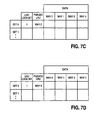
- Figures 7A - 7D illustrate an example of the organization of a cache memory prior to and after a non-temporal instruction hits way 2 of cache set 0.
- This example corresponds to item 3 of Figure 4 and may be implemented by setting a mode bit located in the L1 cache controller to zero (see Figure 4).
- LRU lock bit 70 0 had been previously cleared for cache set 0.
- a non-temporal cache hit does not update the LRU lock bit 70. Accordingly, since the cache set 0 was hit by a non-temporal instruction, neither the LRU lock bit 70 0 nor the LRU bit 60 0 is updated.
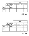
- Figures 8A - 8D illustrate another example of the organization of a cache memory prior to and after a non-temporal instruction hits way 2 of cache set 0.
- This example corresponds to item 4 of Figure 4 and may be implemented by setting the mode bit located in the L1 cache controller to one (see Figure 4).
- LRU lock bit 70 0 had been previously cleared for cache set 0.
- a non-temporal cache hit updates the LRU lock bit 70. Accordingly, as shown in Figure 8A, since the cache set 0 was hit by a non-temporal instruction, the LRU lock bit 70 0 is updated (set to 1), as shown in Figure 8B.
- the LRU bits 60 0 are updated to indicate the way that was hit. In the case where LRU lock bit 70 0 had been previously set for cache set 0 ( Figures 8C and 8D), the LRU lock bit 70 0 remains set to 1. In addition, the LRU bits 60 0 are forced to point to the way within the set that was hit.
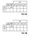
- Figures 9A and 9B illustrate one example of the organization of a cache memory prior to and after a temporal instruction miss to cache set 0.
- This example corresponds to item 5 of Figure 4.
- LRU lock bit 70 0 had been previously set for cache set 0, and since there is a miss by a temporal instruction targeting set 0, the LRU lock bit 70 0 is cleared for that set, upon replacing the temporal miss in the cache.
- the LRU bit 60 0 is updated in accordance with the LRU technique implemented.
- the pseudo LRU technique indicates that way 3 is the least recently used entry.
- Figures 10A - 10B illustrate an example of the organization of a cache memory prior to and after a non-temporal instruction miss to cache set 0. This example corresponds to item 6 of Figure 4.
- LRU lock bit 70 0 had been previously cleared for cache set 0. Since there is a non-temporal miss to cache set 0, the LRU lock bit 70 0 is set and the LRU bits 60 0 remain the same, in order to point to the non-temporal data in the corresponding set 0.
- a shared cache structure for managing temporal and non-temporal instructions, which minimizes data pollution in cache or cache hierarchy is provided.
- Implementation of the present invention also eliminates the use of a separate buffer, making its implementation both cost effective and efficient.
Landscapes
- Engineering & Computer Science (AREA)
- Theoretical Computer Science (AREA)
- Physics & Mathematics (AREA)
- General Engineering & Computer Science (AREA)
- General Physics & Mathematics (AREA)
- Memory System Of A Hierarchy Structure (AREA)
Description
- The present invention relates in general to the field of processors, and in particular, to a technique of providing a shared cache structure for temporal and non-temporal instructions.
- The use of a cache memory with a processor facilitates the reduction of memory access time. The fundamental idea of cache organization is that by keeping the most frequently accessed instructions and data in the fast cache memory, the average memory access time will approach the access time of the cache. To achieve the maximum possible speed of operation, typical processors implement a cache hierarchy, that is, different levels of cache memory. The different levels of cache correspond to different distances from the processor core. The closer the cache is to the processor, the faster the data access. However, the faster the data access, the more costly it is to store data. As a result, the closer the cache level, the faster and smaller the cache.
- The performance of cache memory is frequently measured in terms of its hit ratio. When the processor refers to memory and finds the word in cache, it is said to produce a hit. If the word is not found in cache, then it is in main memory and it counts as a miss. If a miss occurs, then an allocation is made at the entry indexed by the access. The access can be for loading data to the processor or storing data from the processor to memory. The cached information is retained by the cache memory until it is no longer needed, made invalid or replaced by other data, in which instances the cache entry is de-allocated.
- In processors implementing a cache hierarchy, such as the Pentium Pro™ processors which have an L1 and an L2 cache, the faster and smaller L1 cache is located closer to the processor than the L2 cache. When the processor requests cacheable data, for example, a load instruction, the request is first sent to the L1 cache. If the requested data is in the L1 cache, it is provided to the processor. Otherwise, there is an L1 miss and the request is transferred to the L2 cache. Likewise, if there is an L2 cache hit, the data is passed to the L1 cache and the processor core. If there is an L2 cache miss, the request is transferred to main memory. The main memory responds to the L2 cache miss by providing the requested data to the L2 cache, the L1 cache, and to the processor core.
- The type of data that is typically stored in cache includes active portions of programs and data. When the cache is full, it is necessary to replace existing lines of stored data in the cache memory to make room for newly requested lines of data. One such replacement technique involves the use of the least recently used (LRU) algorithm, which replaces the least recently used line of data with the newly requested line. In the Pentium Pro™ processors, since the L2 cache is larger than the L1 cache, the L2 cache typically stores everything in the L1 cache and some additional lines that have been replaced in the L1 cache by the LRU algorithm.
- US-A-5,546,559 discloses a CPU issuing an access instruction to desired data in a main memory, the desired data being in the form of plural entries. If the desired data is not present in any of the plural entries, the desired data is read from the main memory. In such an event an empty entry is searched from the plural entries. If there is no empty entry, an entry is selected which is not set with re-use information in a control information area of the entry, the re-use information instructing to preferentially maintain the data in the data field of the entry. The data of the selected entry is replaced by the data read from the main memory. Re-use information in an access instruction from the CPU for maintaining data in a particular entry is set to the re-use information setting field.
- US-A-5,493,667 discloses an instruction locking method for a cache memory. A two-set associative instruction cache utilises a least recently used (LRU) unit to effectively block a first portion of the instruction cache to allow high speed and predictable execution time for time critical program code sections residing in the first portion while leaving another portion of the instruction cache free to operate in an instruction cache for other non-critical code sections.
- US-A-5,353,425 discloses a memory system having a main memory and a cache memory with locking bits associated with each line in the cache, the locking bits being supplied in a tag table.
- W096/30,836A discloses cache misses being stored in a FIFO missed stack which is searched for displacement patterns to predict a succeeding cache missed by pre-fetching data from main memory identified by a predictive address. Patterns yielding information to develop the predictive address are disclosed so as to determine a least recently used status of data.
- U.S. Patent Application serial number 08/767,950 filed December 17, 1996, entitled "Cache Hierarchy Management" discloses a technique for allocating cache memory through the use of a locality hint associated with an instruction. When a processor accesses memory for transfer of data between the processor and the memory, that access can be allocated to the various levels of cache, or not allocated to cache memory at all, according to the locality hint associated with the instruction. Certain instructions are used infrequently. For example, non-temporal prefetch instructions preload data which the processor does not require immediately, but which are anticipated to be required in the near future. Such data is typically used only once or will not be reused in the immediate future, and is termed "non-temporal data". Instructions that are frequently used are termed "temporal data". For non-temporal data, since the data is used infrequently, optimal performance dictates that the cached application code and data not be overwritten by this infrequently used data. U.S. Application serial number 08/767,950 and EP-A-04 96439 solves this problem by providing a buffer, separate from the cache memory, for storing the infrequently used data, such as non-temporal prefetched data. However, the use of an extra, separate buffer is expensive both in terms of cost and space.
- Accordingly, there is a need in the technology for providing a shared cache structure for temporal and non-temporal instructions, which eliminates the use of a separate buffer.
- According to a first aspect of this invention there is provided a computer system as claimed in
claim 1 herein. - According to a second aspect of this invention there is provided a method as claimed in
claim 4 herein. - Preferred features of the invention are defined by the dependent claims.
- The invention is illustrated by way of example, and not limitation, in the figures. Like reference indicate similar elements.
- Figure 1 illustrates a circuit block diagram of one embodiment of a computer system which implements the present invention, in which a cache memory is used for data accesses between a main memory and a processor of the computer system.
- Figure 2 is a circuit block diagram of a second embodiment of a computer system which implements the present invention, in which two cache memories are arranged into cache memory levels for accessing data between a main memory and a processor(s) of the computer system.
- Figure 3 is a block diagram illustrating one embodiment of the organizational structure of the cache memory in which the technique of the present invention is implemented.
- Figure 4 is a table illustrating the cache management technique, according to one embodiment of the present invention.
- Figures 5A and 5B illustrate one example of the organization of a cache memory prior to and after temporal instruction hits
way 2 of cache set 0, according to one embodiment of the present invention. - Figures 6A and 6B illustrate another example of the organization of a cache memory prior to and after temporal instruction hits
way 2 of cache set 0, according to one embodiment of the present invention. - Figures 7A - 7D illustrate a example of the organization of a cache memory prior to and after a non-temporal instruction hits
way 2 of cache set 0, according to one embodiment of the present invention. - Figures 8A 8D illustrate another example of the organization of a cache memory prior to and after a non-temporal instruction hits
way 2 of cache set 0, according to one embodiment of the present invention. - Figures 9A and 9B illustrate one example of the organization of a cache memory prior to and after a temporal instruction miss to cache set 0, according to one embodiment of the present invention.
- Figures 10A and 10B illustrate an example of the organization of a cache memory prior to and after a non-temporal instruction miss to cache set 0, according to one embodiment of the present invention.
- A technique is described for providing management of cache memories, in which cache allocation is determined by data utilization. In the following description, numerous specific details are set forth, such as specific memory devices, circuit diagrams, processor instructions, etc., in order to provide a thorough understanding of the present invention. However, it will be appreciated by one skilled in the art that the present invention may be practiced without these specific details. In other instances, well known techniques and structures have not been described in detail in order not to obscure the present invention. It is to be noted that a particular implementation is described as a preferred embodiment of the present invention, however, it is readily understood that other embodiments can be designed and implemented without departing from the scope of the present invention. Furthermore, it is appreciated that the present invention is described in reference to a serially arranged cache hierarchy system, but it need not be limited strictly to such a hierarchy.
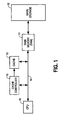
- Referring to Figure 1, a typical computer system is shown, wherein a
processor 10, which forms the central processing unit (CPU) of the computer system is coupled to amain memory 11 by abus 14. Themain memory 11 is typically comprised of a random-access-memory and is usually referred to as RAM. Subsequently, themain memory 11 is generally coupled to amass storage device 12, such as a magnetic or optical memory device, for mass storage (or saving) of information. A cache memory 13 (hereinafter also referred simply as cache) is also coupled to thebus 14. Thecache 13 is shown located between theCPU 11 and themain memory 11, in order to exemplify the functional utilization and transfer of data associated with thecache 13. It is appreciated that the actual physical placement of thecache 13 can vary depending on the system and the processor architecture. Furthermore, acache controller 15 is shown coupled to thecache 13 and thebus 14 for controlling the operation of thecache 13. The operation of a cache controller, such as thecontroller 15, is known in the art and, accordingly, in the subsequent Figures, cache controllers are not illustrated. It is presumed that some controller(s) is/are present under control of theCPU 10 to control the operation of cache(s) shown. - In operation, information transfer between the
memory 11 and theCPU 10 is achieved by memory accesses from theCPU 10. When cacheable data is currently or shortly to be accessed by theCPU 10, that data is first allocated in thecache 13. That is, when theCPU 10 accesses a given information from thememory 11, it seeks the information from thecache 13. If the accessed data is in thecache 13, a "hit" occurs. Otherwise, a "miss" results and cache allocation for the data is sought. As currently practiced, most accesses (whether load or store) require the allocation of thecache 13. Only uncacheable accesses are not allocated in the cache. - Referring to Figure 2, a computer system implementing a multiple cache arrangement is shown. The
CPU 10 is still coupled to themain memory 11 by thebus 14 and thememory 11 is then coupled to themass storage device 12. However, in the example of Figure 2, twoseparate cache memories L1 cache 21 is shown as part of theCPU 10, while theL2 cache 22 is shown external to theCPU 10. This structure exemplifies the current practice of placing the L1 cache on the processor chip while lower level caches are placed external to it, where the lower level caches are further from the processor core. The actual placement of the various cache memories is a design choice or dictated by the processor architecture. Thus, it is appreciated that the L1 cache could be placed external to theCPU 10. - Generally,
CPU 10 includes anexecution unit 23,register file 24 and fetch/decoder unit 25. Theexecution unit 23 is the processing core of theCPU 10 for executing the various arithmetic (or non-memory) processor instructions. Theregister file 24 is a set of general purpose registers for storing (or saving) various information required by theexecution unit 23. There may be more than one register file in more advanced systems. The fetch/decoder unit 25 fetches instructions from a storage location (such as the main memory 11) holding the instructions of a program that will be executed and decodes these instructions for execution by theexecution unit 23. In more advanced processors utilizing pipelined architecture, future instructions are prefetched and decoded before the instructions are actually needed so that the processor is not idle waiting for the instructions to be fetched when needed. - The various units 23-25 of the
CPU 10 are coupled to aninternal bus structure 27. A bus interface unit (BIU) 26 provides an interface for coupling the various units ofCPU 10 to thebus 14. As shown in Figure 2, the L1 cache is coupled to theinternal bus 27 and functions as an internal cache for theCPU 10. However, again it is to be emphasized that the L1 cache could reside outside of theCPU 10 and coupled to thebus 14. The caches can be used to cache data, instructions or both. In some systems, the L1 cache is actually split into two sections, one section for caching data and one section for caching instructions. However, for simplicity of explanation, the various caches described in the Figures are shown as single caches with data, instructions and other information all referenced herein as data. It is appreciated that the operations of the units shown in Figure 2 are known. Furthermore it is appreciated that theCPU 10 actually includes many more components than just the components shown. Thus, only those structures pertinent to the understanding of the present invention are shown in Figure 2. In one embodiment, the invention is utilized in systems having data caches. However, the invention is applicable to any type of cache. - It is also to be noted that the computer system may be comprised of more than one CPU (as shown by the dotted line in Figure 2). In such a system, it is typical for multiple CPUs to share the
main memory 11 and/ormass storage unit 12. Accordingly, some or all of the caches associated with the computer system may be shared by the various processors of the computer system. For example, with the system of Figure 2,L1 cache 21 of each processor would be utilized by its processor only, but themain memory 11 would be shared by all of the CPUs of the system. In addition, each CPU has an associatedexternal L2 cache 22. - The invention can be practiced in a single CPU computer system or in a multiple CPU computer system. It is further noted that other types of units (other than processors) which access memory can function equivalently to the CPUs described herein and, therefore, are capable of performing the memory accessing functions similar to the described CPUs. For example, direct memory accessing (DMA) devices can readily access memory similar to the processors described herein. Thus, a computer system having one processor (CPU), but one or more of the memory accessing units would function equivalent to the multiple processor system shown described herein.
- As noted, only two caches 21-22 are shown. However, the computer system need not be limited to only two levels of cache. It is now a practice to utilize a third level (L3) cache in more advanced systems. It is also the practice to have a serial arrangement of cache memories so that data cached in the L1 cache is also cached in the L2 cache. If there happens to be an L3 cache, then data cached in the L2 cache is typically cached in the L3 cache as well. Thus, data cached at a particular cache level is also cached at all higher levels of the cache hierarchy.
- Figure 3 is a block diagram illustrating one embodiment of the organizational structure of the cache memory in which the technique of the present invention is implemented. In general, there are "x" sets in a cache structure, "y" ways per set (where y ≥ 2), and where each way contains one data entry or one cache line. The invention provides an LRU lock bit which indicates whether any one of the ways within that set contains non-temporal (NT) data. If so, the regular or pseudo LRU bits will be updated to point to the NT data. There are also "z" regular or pseudo LRU bits per set. Unless the LRU lock bit is set, the regular or pseudo LRU bits point to the way within the set in accordance with the least recently used technique implemented. The number of regular or pseudo-LRU bits per set varies depending on the number of ways per set and the LRU (regular or pseudo) technique implemented.
- In the embodiment as shown, the
cache 50 is organized as a four-way set associative cache. In the example of Figure 3, each page is shown as being equal to one-fourth the cache size. In particular, thecache 50 is divided into four ways (for example, way 0 (52), way 1 (54), way 2 (56) and way 3 (58)) of equal size and main memory 21 (see also Figures 1 and 2) is viewed as divided into pages (e.g., page 0 - page n). In another embodiment, each page may be larger or smaller than the cache size. The organizational structure of cache 50 (as shown in Figure 3) may be implemented within thecache 13 of Figure 1, the L1 cache and/orL2 cache 22 of Figure 2. - The
cache 50 also includes an array of least recently used (LRU) bits 600 - 60n each of which points to the way within a set with the least recently used data (or NT data, if a biased LRU technique is implemented). Such listing is performed in accordance with an LRU technique under the control of thecache controller 15, to determine which cache entry to overwrite in the event that a cache set is full. The LRU logic (not shown) keeps track of the cache locations within a set that have been least recently used. In one embodiment, an LRU technique that strictly keeps track of the least-recently used directory algorithm may be implemented. In one alternative embodiment, a pseudo-LRU algorithm which makes a best attempt at keeping track of the least recently used directory element, is implemented. For discussion purposes, the bits 600 - 60n will be referred to as LRU bits 600 - 60n, while the array of LRU bits 600 - 60n will be referred to asLRU bits 60. - The
cache 50 further includes an array of LRU lock bits 700 - 70n which indicates whether any of theways - Figure 4 is a table illustrating the cache management technique in accordance with the principles of the present invention. The invention utilizes the array of LRU lock bits 700 - 70n to indicate whether any of the corresponding cached data is streaming or non-temporal, and as such, would be the first entry to be replaced upon a cache miss to the corresponding set. In one embodiment, the
LRU lock bit 70, when set to 1, indicates that the corresponding set has an entry that is non-temporal. If theLRU lock bit 70 is cleared, upon a cache hit by a temporal instruction, the corresponding LRU bit(s) 60 is(are) updated in accordance with the LRU technique implemented (seeitem 1 of Figure 4) and the associated LRU lock bit is not updated. However, if theLRU lock bit 70 is already set to 1 (indicating that the corresponding set has a non-temporal instruction), theLRU lock bit 70 is not updated, and theLRU bit 60 is not updated (see item 2). - In the case of a cache hit by a non-temporal instruction, the
LRU bit 60 and theLRU lock bit 70 are not updated, regardless of the status of the LRU lock bit 70 (see item 3). In an alternate embodiment, as controlled through a mode bit in a control register in the L1 cache controller, cache hits by a streaming or non-temporal instructions force the LRU bits to the way that was hit (see item 4). In addition, theLRU lock bit 70 is set to 1. In this embodiment, the data hit by the streaming or non-temporal instruction will be the first to be replaced upon a cache miss to the corresponding set. - Upon a cache miss by a temporal instruction, the LRU lock bit is cleared and the
LRU bit 60 is updated (item 5) based on a pseudo LRU technique. However, upon a cache miss by a streaming or non-temporal instruction, theLRU lock bit 70 is set to 1 and the correspondingLRU bit 60 is not updated (item 6). - Examples of each of the items provided in the table of Figure 4 will now be discussed. Figures 5A and 5B illustrate one example of the organization of a cache memory prior to and after temporal instruction hits
way 2 ofcache set 0. This example corresponds toitem 1 of Figure 4. Here,LRU lock bit 700 had been previously cleared for cache set 0, and since the cache set 0 was hit by a temporal instruction, theLRU lock bit 700 is not updated. However, theLRU bit 600 is updated in accordance with the LRU technique implemented. In the example, it is assumed that the pseudo LRU technique indicates thatway 3 is the least recently used entry. - Figures 6A and 6B illustrate another example of the organization of a cache memory prior to and after temporal instruction hits
way 2 ofcache set 0. This example corresponds toitem 2 of Figure 4. Here,LRU lock bit 700 had been previously set for cache set 0, indicating that the corresponding set contains non-temporal data. Accordingly, neither theLRU lock bit 700 nor theLRU bit 600 is updated. - Figures 7A - 7D illustrate an example of the organization of a cache memory prior to and after a non-temporal instruction hits
way 2 ofcache set 0. This example corresponds toitem 3 of Figure 4 and may be implemented by setting a mode bit located in the L1 cache controller to zero (see Figure 4). In the first case (Figures 7A and 7B),LRU lock bit 700 had been previously cleared forcache set 0. In this embodiment, a non-temporal cache hit does not update theLRU lock bit 70. Accordingly, since the cache set 0 was hit by a non-temporal instruction, neither theLRU lock bit 700 nor theLRU bit 600 is updated. In the second case (Figures 7C and 7D),LRU lock bit 700 had been previously set for cache set 0, indicating that the corresponding set contains non-temporal data. Accordingly, neither theLRU lock bit 700 nor theLRU bit 600 is updated. - Figures 8A - 8D illustrate another example of the organization of a cache memory prior to and after a non-temporal instruction hits
way 2 ofcache set 0. This example corresponds toitem 4 of Figure 4 and may be implemented by setting the mode bit located in the L1 cache controller to one (see Figure 4). In the first case (Figures 8A and 8B),LRU lock bit 700 had been previously cleared forcache set 0. In this example of an alternate embodiment to that example shown in Figures 7A-7D, a non-temporal cache hit updates theLRU lock bit 70. Accordingly, as shown in Figure 8A, since the cache set 0 was hit by a non-temporal instruction, theLRU lock bit 700 is updated (set to 1), as shown in Figure 8B. In addition, theLRU bits 600 are updated to indicate the way that was hit. In the case whereLRU lock bit 700 had been previously set for cache set 0 (Figures 8C and 8D), theLRU lock bit 700 remains set to 1. In addition, theLRU bits 600 are forced to point to the way within the set that was hit. - Figures 9A and 9B illustrate one example of the organization of a cache memory prior to and after a temporal instruction miss to
cache set 0. This example corresponds toitem 5 of Figure 4. Here,LRU lock bit 700 had been previously set for cache set 0, and since there is a miss by a temporalinstruction targeting set 0, theLRU lock bit 700 is cleared for that set, upon replacing the temporal miss in the cache. However, theLRU bit 600 is updated in accordance with the LRU technique implemented. In the example, the pseudo LRU technique indicates thatway 3 is the least recently used entry. - Figures 10A - 10B illustrate an example of the organization of a cache memory prior to and after a non-temporal instruction miss to
cache set 0. This example corresponds toitem 6 of Figure 4. In this case,LRU lock bit 700 had been previously cleared forcache set 0. Since there is a non-temporal miss to cache set 0, theLRU lock bit 700 is set and theLRU bits 600 remain the same, in order to point to the non-temporal data in thecorresponding set 0. - By implementing the apparatus and method of the present invention, a shared cache structure for managing temporal and non-temporal instructions, which minimizes data pollution in cache or cache hierarchy is provided. Implementation of the present invention also eliminates the use of a separate buffer, making its implementation both cost effective and efficient.
- The present invention may be embodied in other specific forms without departing from its essential characteristics. The described embodiments are to be considered in all respects only as illustrative and not restrictive. The scope of the invention is, therefore, indicated by the appended claims rather than the foregoing description. All changes which come within the meaning and range of equivalency of the claims are to be embraced within their scope.
Claims (18)
- A computer system having cache memory management, the computer system comprising:a main memory (11);a processor (10) coupled to said main memory, said processor to execute instructions to process non-temporal data and temporal data;at least one cache memory (50) coupled to said processor, said at least one cache memory having at least two cache ways, each of said at least two cache ways comprising a plurality of sets of data stored in said at least one cache memory, each of said plurality of sets of data having a first bit 10o-10n and z second bits 60o-60n in said at least one cache memory, the number z of second bits depending on the number of ways per set and a least recently used technique implemented, said z second bits pointing to the entry to be replaced upon a cache miss to the corresponding set, said first bit of each of said plurality of sets of data to indicate whether any one of said at least two cache ways in the associated set of data contains said non-temporal data that can be replaced first, said non-temporal data being infrequently used by the processor,wherein if said first bit indicates that one of said at least two cache ways in the associated set of data contains said non-temporal data, the z second bits point to the said non-temporal data, and if said first bit indicates that one of said at least two cache ways in the associated set of data does not contain said non-temporal data, the z second bits point to the cache way within the associated set of data in accordance with the least recently used technique,; and
wherein said processor accesses data from one of said main memory or said at least one cache memory. - The computer system of claim 1, further comprising:cache control logic (15) coupled to said at least one cache memory and said processor, said cache control logic to control said at least one cache memory.
- The computer system of claim 2, wherein said processor receives an instruction for accessing data, said processor determining if said data is located in said at least one cache memory, if so, accessing said data from said at least one cache memory, otherwise, accessing said data from said main memory.
- A method in a computer system of allocating cache memory for replacement, the method comprising:providing a main memory (11);providing a processor (10) coupled to said main memory, said processor to execute instructions to process non-temporal data and temporal data;providing at least one cache memory (50) coupled to said processor, said at least one cache memory having at least two cache ways, each of said at least two cache ways comprising a plurality of sets of data stored in said least one cache memory, each of said plurality of sets of data having a first bit (70o-70n) and z second bits (60o-60n) in said at least one cache memory, the number z of second bits depending on the number of ways per set and a least recently used technique implemented, said z second bits pointing to the entry to be replaced upon a cache miss to the corresponding set, said first bit of each of said plurality of sets of data to indicate whether any one of said at least two cache ways in the associated set of data contains said non-temporal data that can be replaced first, said non-temporal data being infrequently used by the processor, wherein if said first bit indicates that one of said at least two cache ways in the associated set of data contains said non-temporal data, the z second bits point to the said non-temporal data, and if said first bit indicates that one of said at least two cache ways in the associated set of data does not contain said non-temporal data, the z second bits point to the cache way within the associated set of data in accordance with the least recently used technique,; andaccessing, by said processor, data from one of said main memory or said at least one cache memory.
- The method of claim 4, wherein the associated set of data does not contain said non-temporal data and said z second bits point to the data entry which is a least recently used entry by the processor with respect to other data entries in the associated set of data.
- The method of claim 4, wherein said first bit is set to indicate that one of said at least two cache ways in the associated set of data contains said non-temporal data which will be replaced upon a cache miss.
- The method of claim 6, wherein the associated set of data contains said non-temporal data and said z second bits point to said non-temporal data in one of said at least two cache ways in the associated set of data.
- The method of claim 4, wherein said first bit is cleared to indicate that none of said at least two cache ways in the associated set of data contains said non-temporal data.
- The method of any preceding claim, further comprising:providing a cache control logic (15) coupled to said at least one cache memory and said processor, said cache control logic controlling said at least one cache memory.
- The method of claim 9, wherein said processor receives an instruction for accessing data, said processor determining if said data is located in said at least one cache memory, if so, accessing said data from said at least one cache memory, otherwise, accessing said data from said main memory.
- The method of claim 10, wherein upon a cache bit by a temporal instruction if said first bit is not set to indicate non-temporal data then updating said z second bits in accordance with said least recently used technique otherwise leaving said z second bits unchanged.
- The method of claim 10, wherein said first bit associated with the set of data of said way being accessed is unchanged.
- The method of claim 10, wherein upon a cache bit by a non-temporal instruction, configuring said first bit to indicate that said accessed data is non-temporal, and updating said z second bits to indicate the way that was bit.
- The method of claim 10, wherein upon a cache miss by a non-temporal instruction configuring said first bit to indicate that said data is non-temporal, said z second bits being left unchanged in order to point to said non-temporal data.
- The method of claim 14, wherein upon a cache miss by a temporal instruction configuring said first bit to indicate that said accessed data is temporal, and updating said z second bits in accordance with said least recently used technique.
- The method of any preceding claim, wherein said first bit of each of said plurality of sets of data is a lock bit.
- The method of any preceding claim, wherein said non-temporal data is a type of data that is predetermined to be infrequently used by the processor.
- The method of any preceding claim, wherein said non-temporal data is a type of data that is streaming data.
Applications Claiming Priority (3)
| Application Number | Priority Date | Filing Date | Title |
|---|---|---|---|
| US09/053,386 US6202129B1 (en) | 1998-03-31 | 1998-03-31 | Shared cache structure for temporal and non-temporal information using indicative bits |
| US53386 | 1998-03-31 | ||
| PCT/US1999/006501 WO1999050752A1 (en) | 1998-03-31 | 1999-03-24 | Shared cache structure for temporal and non-temporal instructions |
Publications (3)
| Publication Number | Publication Date |
|---|---|
| EP1066566A1 EP1066566A1 (en) | 2001-01-10 |
| EP1066566A4 EP1066566A4 (en) | 2002-10-23 |
| EP1066566B1 true EP1066566B1 (en) | 2006-11-02 |
Family
ID=21983863
Family Applications (1)
| Application Number | Title | Priority Date | Filing Date |
|---|---|---|---|
| EP99915030A Expired - Lifetime EP1066566B1 (en) | 1998-03-31 | 1999-03-24 | Shared cache structure for temporal and non-temporal instructions and corresponding method |
Country Status (10)
| Country | Link |
|---|---|
| US (2) | US6202129B1 (en) |
| EP (1) | EP1066566B1 (en) |
| JP (1) | JP4486750B2 (en) |
| KR (1) | KR100389549B1 (en) |
| CN (1) | CN1230750C (en) |
| AU (1) | AU3364599A (en) |
| BR (1) | BR9909295A (en) |
| RU (1) | RU2212704C2 (en) |
| TW (1) | TW573252B (en) |
| WO (1) | WO1999050752A1 (en) |
Families Citing this family (68)
| Publication number | Priority date | Publication date | Assignee | Title |
|---|---|---|---|---|
| US5978379A (en) | 1997-01-23 | 1999-11-02 | Gadzoox Networks, Inc. | Fiber channel learning bridge, learning half bridge, and protocol |
| US6202129B1 (en) * | 1998-03-31 | 2001-03-13 | Intel Corporation | Shared cache structure for temporal and non-temporal information using indicative bits |
| US6216215B1 (en) | 1998-04-02 | 2001-04-10 | Intel Corporation | Method and apparatus for senior loads |
| US6542966B1 (en) * | 1998-07-16 | 2003-04-01 | Intel Corporation | Method and apparatus for managing temporal and non-temporal data in a single cache structure |
| US7430171B2 (en) | 1998-11-19 | 2008-09-30 | Broadcom Corporation | Fibre channel arbitrated loop bufferless switch circuitry to increase bandwidth without significant increase in cost |
| US6560677B1 (en) * | 1999-05-04 | 2003-05-06 | International Business Machines Corporation | Methods, cache memories, systems and computer program products for storing transient, normal, and locked entries in an associative cache memory |
| US6728835B1 (en) * | 2000-08-30 | 2004-04-27 | Unisys Corporation | Leaky cache mechanism |
| US6681295B1 (en) * | 2000-08-31 | 2004-01-20 | Hewlett-Packard Development Company, L.P. | Fast lane prefetching |
| US6578111B1 (en) * | 2000-09-29 | 2003-06-10 | Sun Microsystems, Inc. | Cache memory system and method for managing streaming-data |
| US6598124B1 (en) * | 2000-09-29 | 2003-07-22 | Sun Microsystems, Inc. | System and method for identifying streaming-data |
| WO2002027498A2 (en) * | 2000-09-29 | 2002-04-04 | Sun Microsystems, Inc. | System and method for identifying and managing streaming-data |
| US6668307B1 (en) * | 2000-09-29 | 2003-12-23 | Sun Microsystems, Inc. | System and method for a software controlled cache |
| US6766413B2 (en) * | 2001-03-01 | 2004-07-20 | Stratus Technologies Bermuda Ltd. | Systems and methods for caching with file-level granularity |
| US7287649B2 (en) * | 2001-05-18 | 2007-10-30 | Broadcom Corporation | System on a chip for packet processing |
| US6574708B2 (en) * | 2001-05-18 | 2003-06-03 | Broadcom Corporation | Source controlled cache allocation |
| US6766389B2 (en) | 2001-05-18 | 2004-07-20 | Broadcom Corporation | System on a chip for networking |
| US7239636B2 (en) | 2001-07-23 | 2007-07-03 | Broadcom Corporation | Multiple virtual channels for use in network devices |
| US6823426B2 (en) * | 2001-12-20 | 2004-11-23 | Intel Corporation | System and method of data replacement in cache ways |
| US7328328B2 (en) * | 2002-02-19 | 2008-02-05 | Ip-First, Llc | Non-temporal memory reference control mechanism |
| US7295555B2 (en) | 2002-03-08 | 2007-11-13 | Broadcom Corporation | System and method for identifying upper layer protocol message boundaries |
| US7114043B2 (en) * | 2002-05-15 | 2006-09-26 | Broadcom Corporation | Ambiguous virtual channels |
| US7266587B2 (en) * | 2002-05-15 | 2007-09-04 | Broadcom Corporation | System having interfaces, switch, and memory bridge for CC-NUMA operation |
| US7269709B2 (en) * | 2002-05-15 | 2007-09-11 | Broadcom Corporation | Memory controller configurable to allow bandwidth/latency tradeoff |
| US7035979B2 (en) * | 2002-05-22 | 2006-04-25 | International Business Machines Corporation | Method and apparatus for optimizing cache hit ratio in non L1 caches |
| US7073030B2 (en) | 2002-05-22 | 2006-07-04 | International Business Machines Corporation | Method and apparatus providing non level one information caching using prefetch to increase a hit ratio |
| US6904501B1 (en) * | 2002-06-17 | 2005-06-07 | Silicon Graphics, Inc. | Cache memory for identifying locked and least recently used storage locations |
| US7346701B2 (en) | 2002-08-30 | 2008-03-18 | Broadcom Corporation | System and method for TCP offload |
| US7934021B2 (en) | 2002-08-29 | 2011-04-26 | Broadcom Corporation | System and method for network interfacing |
| US7313623B2 (en) | 2002-08-30 | 2007-12-25 | Broadcom Corporation | System and method for TCP/IP offload independent of bandwidth delay product |
| WO2004021626A2 (en) | 2002-08-30 | 2004-03-11 | Broadcom Corporation | System and method for handling out-of-order frames |
| US8180928B2 (en) | 2002-08-30 | 2012-05-15 | Broadcom Corporation | Method and system for supporting read operations with CRC for iSCSI and iSCSI chimney |
| US7512498B2 (en) * | 2002-12-31 | 2009-03-31 | Intel Corporation | Streaming processing of biological sequence matching |
| EP1686485A4 (en) * | 2003-11-18 | 2008-10-29 | Matsushita Electric Ind Co Ltd | Cache memory and control method thereof |
| US7321954B2 (en) * | 2004-08-11 | 2008-01-22 | International Business Machines Corporation | Method for software controllable dynamically lockable cache line replacement system |
| US20060101208A1 (en) * | 2004-11-09 | 2006-05-11 | Intel Corporation | Method and apparatus for handling non-temporal memory accesses in a cache |
| US7356650B1 (en) * | 2005-06-17 | 2008-04-08 | Unisys Corporation | Cache apparatus and method for accesses lacking locality |
| US7437510B2 (en) * | 2005-09-30 | 2008-10-14 | Intel Corporation | Instruction-assisted cache management for efficient use of cache and memory |
| US7624257B2 (en) * | 2005-11-30 | 2009-11-24 | International Business Machines Corporation | Digital data processing apparatus having hardware multithreading support including a register set reserved for special class threads |
| US20070150658A1 (en) * | 2005-12-28 | 2007-06-28 | Jaideep Moses | Pinning locks in shared cache |
| US8527713B2 (en) * | 2006-01-31 | 2013-09-03 | Qualcomm Incorporated | Cache locking without interference from normal allocations |
| GB0603552D0 (en) | 2006-02-22 | 2006-04-05 | Advanced Risc Mach Ltd | Cache management within a data processing apparatus |
| WO2007097028A1 (en) * | 2006-02-27 | 2007-08-30 | Fujitsu Limited | Lru control device, lru control method, and lru control program |
| US20080147989A1 (en) * | 2006-12-14 | 2008-06-19 | Arm Limited | Lockdown control of a multi-way set associative cache memory |
| KR101165132B1 (en) | 2007-01-31 | 2012-07-12 | 콸콤 인코포레이티드 | Apparatus and methods to reduce castouts in a multi-level cache hierarchy |
| US7793049B2 (en) * | 2007-10-30 | 2010-09-07 | International Business Machines Corporation | Mechanism for data cache replacement based on region policies |
| US8108614B2 (en) * | 2007-12-31 | 2012-01-31 | Eric Sprangle | Mechanism for effectively caching streaming and non-streaming data patterns |
| AU2008359713B2 (en) * | 2008-07-23 | 2012-12-13 | Micro Motion, Inc. | Processing system with external memory access control |
| US8364898B2 (en) * | 2009-01-23 | 2013-01-29 | International Business Machines Corporation | Optimizing a cache back invalidation policy |
| US8312219B2 (en) * | 2009-03-02 | 2012-11-13 | International Business Machines Corporation | Hybrid caching techniques and garbage collection using hybrid caching techniques |
| US8392661B1 (en) * | 2009-09-21 | 2013-03-05 | Tilera Corporation | Managing cache coherence |
| JP5444477B2 (en) * | 2009-12-16 | 2014-03-19 | テレフオンアクチーボラゲット エル エム エリクソン(パブル) | Method, server, computer program, and computer program product for caching |
| US9323527B2 (en) * | 2010-10-15 | 2016-04-26 | International Business Machines Corporation | Performance of emerging applications in a virtualized environment using transient instruction streams |
| US9342453B2 (en) | 2011-09-30 | 2016-05-17 | Intel Corporation | Memory channel that supports near memory and far memory access |
| EP2761480A4 (en) | 2011-09-30 | 2015-06-24 | Intel Corp | Apparatus and method for implementing a multi-level memory hierarchy over common memory channels |
| CN103946812B (en) | 2011-09-30 | 2017-06-09 | 英特尔公司 | Apparatus and method for realizing multi-level memory hierarchy |
| CN103946811B (en) | 2011-09-30 | 2017-08-11 | 英特尔公司 | Apparatus and method for realizing the multi-level store hierarchy with different operation modes |
| WO2013080426A1 (en) * | 2011-12-01 | 2013-06-06 | パナソニック株式会社 | Integrated-circuit device with structure devised in consideration of heat, three-dimensional integrated circuit, three-dimensional processor device, and process scheduler |
| US9519549B2 (en) * | 2012-01-11 | 2016-12-13 | International Business Machines Corporation | Data storage backup with lessened cache pollution |
| US8874852B2 (en) | 2012-03-28 | 2014-10-28 | International Business Machines Corporation | Data cache block deallocate requests in a multi-level cache hierarchy |
| US8856455B2 (en) | 2012-03-28 | 2014-10-07 | International Business Machines Corporation | Data cache block deallocate requests |
| CN103577480B (en) * | 2012-08-07 | 2017-05-31 | 中国银联股份有限公司 | A kind of parameter division system and its method, a kind of transaction processing system and its method |
| US9558121B2 (en) * | 2012-12-28 | 2017-01-31 | Intel Corporation | Two-level cache locking mechanism |
| US9256539B2 (en) | 2013-03-07 | 2016-02-09 | Lenovo Enterprise Solutions (Singapore) Pte. Ltd. | Sharing cache in a computing system |
| US9311239B2 (en) | 2013-03-14 | 2016-04-12 | Intel Corporation | Power efficient level one data cache access with pre-validated tags |
| US20150095586A1 (en) * | 2013-09-30 | 2015-04-02 | Advanced Micro Devices , Inc. | Storing non-temporal cache data |
| US11580125B2 (en) * | 2015-05-08 | 2023-02-14 | Adp, Inc. | Information system with temporal data |
| US10379827B2 (en) * | 2016-12-29 | 2019-08-13 | Intel Corporation | Automatic identification and generation of non-temporal store and load operations in a dynamic optimization environment |
| US11681627B1 (en) * | 2021-10-18 | 2023-06-20 | Meta Platforms Technologies, Llc | Distributed temporal cache for Systems on a Chip |
Family Cites Families (33)
| Publication number | Priority date | Publication date | Assignee | Title |
|---|---|---|---|---|
| JPS5119453A (en) * | 1974-08-08 | 1976-02-16 | Fujitsu Ltd | Patsufua memoriseigyohoshiki |
| JPS5534336A (en) * | 1978-08-31 | 1980-03-10 | Fujitsu Ltd | Buffer memory control method |
| JPS58159285A (en) * | 1982-03-17 | 1983-09-21 | Nec Corp | Buffer memory control system |
| JPH01133162A (en) * | 1987-11-18 | 1989-05-25 | Fujitsu Ltd | Cache memory control system |
| US4905141A (en) | 1988-10-25 | 1990-02-27 | International Business Machines Corporation | Partitioned cache memory with partition look-aside table (PLAT) for early partition assignment identification |
| JPH0358151A (en) * | 1989-07-26 | 1991-03-13 | Nec Corp | Cache memory device |
| JPH0358252A (en) * | 1989-07-27 | 1991-03-13 | Nec Corp | Cache memory controller |
| JPH041838A (en) * | 1990-04-18 | 1992-01-07 | Nec Corp | Cache memory control circuit |
| JPH04215151A (en) * | 1990-12-13 | 1992-08-05 | Nec Commun Syst Ltd | Cache control system |
| EP0496439B1 (en) * | 1991-01-15 | 1998-01-21 | Koninklijke Philips Electronics N.V. | Computer system with multi-buffer data cache and method therefor |
| GB2255211B (en) * | 1991-04-25 | 1995-05-17 | Intel Corp | LRU pointer updating in a controller for two-way set associative cache |
| GB2256512B (en) * | 1991-06-04 | 1995-03-15 | Intel Corp | Second level cache controller unit and system |
| JPH05165726A (en) * | 1991-12-12 | 1993-07-02 | Nec Corp | Data processor |
| JPH05233454A (en) * | 1992-02-24 | 1993-09-10 | Hitachi Ltd | Cache memory device |
| US5353425A (en) * | 1992-04-29 | 1994-10-04 | Sun Microsystems, Inc. | Methods and apparatus for implementing a pseudo-LRU cache memory replacement scheme with a locking feature |
| US5471605A (en) * | 1992-08-27 | 1995-11-28 | Intel Corporation | Apparatus for updating a multi-way set associative cache memory status array |
| US5434992A (en) | 1992-09-04 | 1995-07-18 | International Business Machines Corporation | Method and means for dynamically partitioning cache into a global and data type subcache hierarchy from a real time reference trace |
| US5493667A (en) * | 1993-02-09 | 1996-02-20 | Intel Corporation | Apparatus and method for an instruction cache locking scheme |
| JPH06348595A (en) * | 1993-06-07 | 1994-12-22 | Hitachi Ltd | Cache device |
| JPH07281957A (en) * | 1994-04-15 | 1995-10-27 | Hitachi Ltd | Cache storage and access instruction generation method |
| US5826052A (en) | 1994-04-29 | 1998-10-20 | Advanced Micro Devices, Inc. | Method and apparatus for concurrent access to multiple physical caches |
| JPH07334428A (en) * | 1994-06-14 | 1995-12-22 | Toshiba Corp | Cache memory |
| US5584014A (en) * | 1994-12-20 | 1996-12-10 | Sun Microsystems, Inc. | Apparatus and method to preserve data in a set associative memory device |
| US5701426A (en) * | 1995-03-31 | 1997-12-23 | Bull Information Systems Inc. | Data processing system and method using cache miss address prediction and forced LRU status in a cache memory to improve cache hit ratio |
| US5845317A (en) * | 1995-11-17 | 1998-12-01 | Micron Technology, Inc. | Multi-way cache expansion circuit architecture |
| GB2311880A (en) * | 1996-04-03 | 1997-10-08 | Advanced Risc Mach Ltd | Partitioned cache memory |
| US5829025A (en) * | 1996-12-17 | 1998-10-27 | Intel Corporation | Computer system and method of allocating cache memories in a multilevel cache hierarchy utilizing a locality hint within an instruction |
| JPH10207767A (en) * | 1997-01-16 | 1998-08-07 | Toshiba Corp | Cache memory with lock function and microprocessor equipped with cache memory |
| US6434671B2 (en) * | 1997-09-30 | 2002-08-13 | Intel Corporation | Software-controlled cache memory compartmentalization |
| US6105111A (en) * | 1998-03-31 | 2000-08-15 | Intel Corporation | Method and apparatus for providing a cache management technique |
| US6202129B1 (en) * | 1998-03-31 | 2001-03-13 | Intel Corporation | Shared cache structure for temporal and non-temporal information using indicative bits |
| US6223258B1 (en) * | 1998-03-31 | 2001-04-24 | Intel Corporation | Method and apparatus for implementing non-temporal loads |
| US6205520B1 (en) * | 1998-03-31 | 2001-03-20 | Intel Corporation | Method and apparatus for implementing non-temporal stores |
-
1998
- 1998-03-31 US US09/053,386 patent/US6202129B1/en not_active Expired - Lifetime
-
1999
- 1999-03-24 KR KR10-2000-7010799A patent/KR100389549B1/en not_active IP Right Cessation
- 1999-03-24 BR BR9909295-6A patent/BR9909295A/en not_active Application Discontinuation
- 1999-03-24 JP JP2000541596A patent/JP4486750B2/en not_active Expired - Fee Related
- 1999-03-24 RU RU2000127102/09A patent/RU2212704C2/en not_active IP Right Cessation
- 1999-03-24 CN CNB998047333A patent/CN1230750C/en not_active Expired - Lifetime
- 1999-03-24 WO PCT/US1999/006501 patent/WO1999050752A1/en active IP Right Grant
- 1999-03-24 AU AU33645/99A patent/AU3364599A/en not_active Abandoned
- 1999-03-24 EP EP99915030A patent/EP1066566B1/en not_active Expired - Lifetime
- 1999-03-31 TW TW88105070A patent/TW573252B/en not_active IP Right Cessation
-
2001
- 2001-03-09 US US09/803,357 patent/US6584547B2/en not_active Expired - Lifetime
Also Published As
| Publication number | Publication date |
|---|---|
| CN1230750C (en) | 2005-12-07 |
| KR20010042262A (en) | 2001-05-25 |
| EP1066566A4 (en) | 2002-10-23 |
| WO1999050752A9 (en) | 2000-05-25 |
| JP2002510085A (en) | 2002-04-02 |
| AU3364599A (en) | 1999-10-18 |
| BR9909295A (en) | 2000-12-05 |
| TW573252B (en) | 2004-01-21 |
| JP4486750B2 (en) | 2010-06-23 |
| US20020007441A1 (en) | 2002-01-17 |
| CN1295687A (en) | 2001-05-16 |
| WO1999050752A1 (en) | 1999-10-07 |
| US6202129B1 (en) | 2001-03-13 |
| US6584547B2 (en) | 2003-06-24 |
| KR100389549B1 (en) | 2003-06-27 |
| EP1066566A1 (en) | 2001-01-10 |
| RU2212704C2 (en) | 2003-09-20 |
Similar Documents
| Publication | Publication Date | Title |
|---|---|---|
| EP1066566B1 (en) | Shared cache structure for temporal and non-temporal instructions and corresponding method | |
| US6105111A (en) | Method and apparatus for providing a cache management technique | |
| US6957304B2 (en) | Runahead allocation protection (RAP) | |
| US7783837B2 (en) | System and storage medium for memory management | |
| US6219760B1 (en) | Cache including a prefetch way for storing cache lines and configured to move a prefetched cache line to a non-prefetch way upon access to the prefetched cache line | |
| US4774654A (en) | Apparatus and method for prefetching subblocks from a low speed memory to a high speed memory of a memory hierarchy depending upon state of replacing bit in the low speed memory | |
| US6766419B1 (en) | Optimization of cache evictions through software hints | |
| US5737565A (en) | System and method for diallocating stream from a stream buffer | |
| US7284096B2 (en) | Systems and methods for data caching | |
| US5664147A (en) | System and method that progressively prefetches additional lines to a distributed stream buffer as the sequentiality of the memory accessing is demonstrated | |
| US6292871B1 (en) | Loading accessed data from a prefetch buffer to a least recently used position in a cache | |
| US6085291A (en) | System and method for selectively controlling fetching and prefetching of data to a processor | |
| US7895399B2 (en) | Computer system and control method for controlling processor execution of a prefetech command | |
| EP1149342B1 (en) | Method and apparatus for managing temporal and non-temporal data in a single cache structure | |
| EP1573555B1 (en) | Page descriptors for prefetching and memory management | |
| US7073030B2 (en) | Method and apparatus providing non level one information caching using prefetch to increase a hit ratio | |
| US20050210200A1 (en) | System and method for caching | |
| US20100217937A1 (en) | Data processing apparatus and method | |
| EP1012723A1 (en) | Cache hierarchy management with locality hints for different cache levels | |
| WO1999031593A1 (en) | Cache tag caching | |
| US6668307B1 (en) | System and method for a software controlled cache | |
| US7293141B1 (en) | Cache word of interest latency organization | |
| US5926841A (en) | Segment descriptor cache for a processor | |
| JPH08314802A (en) | Cache system,cache memory address unit and method for operation of cache memory | |
| US11397680B2 (en) | Apparatus and method for controlling eviction from a storage structure |
Legal Events
| Date | Code | Title | Description |
|---|---|---|---|
| PUAI | Public reference made under article 153(3) epc to a published international application that has entered the european phase |
Free format text: ORIGINAL CODE: 0009012 |
|
| 17P | Request for examination filed |
Effective date: 20001030 |
|
| AK | Designated contracting states |
Kind code of ref document: A1 Designated state(s): FR IT |
|
| A4 | Supplementary search report drawn up and despatched |
Effective date: 20020905 |
|
| AK | Designated contracting states |
Kind code of ref document: A4 Designated state(s): FR IT |
|
| RIC1 | Information provided on ipc code assigned before grant |
Free format text: 7G 06F 12/08 A, 7G 06F 12/12 B |
|
| 17Q | First examination report despatched |
Effective date: 20040310 |
|
| GRAP | Despatch of communication of intention to grant a patent |
Free format text: ORIGINAL CODE: EPIDOSNIGR1 |
|
| RTI1 | Title (correction) |
Free format text: SHARED CACHE STRUCTURE FOR TEMPORAL AND NON-TEMPORAL INSTRUCTIONS AND CORRESPONDING METHOD |
|
| GRAS | Grant fee paid |
Free format text: ORIGINAL CODE: EPIDOSNIGR3 |
|
| GRAA | (expected) grant |
Free format text: ORIGINAL CODE: 0009210 |
|
| AK | Designated contracting states |
Kind code of ref document: B1 Designated state(s): FR IT |
|
| PG25 | Lapsed in a contracting state [announced via postgrant information from national office to epo] |
Ref country code: IT Free format text: LAPSE BECAUSE OF FAILURE TO SUBMIT A TRANSLATION OF THE DESCRIPTION OR TO PAY THE FEE WITHIN THE PRESCRIBED TIME-LIMIT;WARNING: LAPSES OF ITALIAN PATENTS WITH EFFECTIVE DATE BEFORE 2007 MAY HAVE OCCURRED AT ANY TIME BEFORE 2007. THE CORRECT EFFECTIVE DATE MAY BE DIFFERENT FROM THE ONE RECORDED. Effective date: 20061102 |
|
| ET | Fr: translation filed | ||
| PLBE | No opposition filed within time limit |
Free format text: ORIGINAL CODE: 0009261 |
|
| STAA | Information on the status of an ep patent application or granted ep patent |
Free format text: STATUS: NO OPPOSITION FILED WITHIN TIME LIMIT |
|
| 26N | No opposition filed |
Effective date: 20070803 |
|
| REG | Reference to a national code |
Ref country code: FR Ref legal event code: PLFP Year of fee payment: 18 |
|
| PGFP | Annual fee paid to national office [announced via postgrant information from national office to epo] |
Ref country code: FR Payment date: 20160223 Year of fee payment: 18 |
|
| REG | Reference to a national code |
Ref country code: FR Ref legal event code: ST Effective date: 20171130 |
|
| PG25 | Lapsed in a contracting state [announced via postgrant information from national office to epo] |
Ref country code: FR Free format text: LAPSE BECAUSE OF NON-PAYMENT OF DUE FEES Effective date: 20170331 |