EP1061453A1 - Transmission system and interface and interface device between a parallel bus system and a transmitter/receiver - Google Patents
Transmission system and interface and interface device between a parallel bus system and a transmitter/receiver Download PDFInfo
- Publication number
- EP1061453A1 EP1061453A1 EP00202011A EP00202011A EP1061453A1 EP 1061453 A1 EP1061453 A1 EP 1061453A1 EP 00202011 A EP00202011 A EP 00202011A EP 00202011 A EP00202011 A EP 00202011A EP 1061453 A1 EP1061453 A1 EP 1061453A1
- Authority
- EP
- European Patent Office
- Prior art keywords
- signal
- data
- clock
- bits
- internal clock
- Prior art date
- Legal status (The legal status is an assumption and is not a legal conclusion. Google has not performed a legal analysis and makes no representation as to the accuracy of the status listed.)
- Withdrawn
Links
Images


Classifications
-
- G—PHYSICS
- G06—COMPUTING; CALCULATING OR COUNTING
- G06F—ELECTRIC DIGITAL DATA PROCESSING
- G06F13/00—Interconnection of, or transfer of information or other signals between, memories, input/output devices or central processing units
- G06F13/38—Information transfer, e.g. on bus
- G06F13/42—Bus transfer protocol, e.g. handshake; Synchronisation
- G06F13/4282—Bus transfer protocol, e.g. handshake; Synchronisation on a serial bus, e.g. I2C bus, SPI bus
- G06F13/4295—Bus transfer protocol, e.g. handshake; Synchronisation on a serial bus, e.g. I2C bus, SPI bus using an embedded synchronisation
-
- G—PHYSICS
- G06—COMPUTING; CALCULATING OR COUNTING
- G06F—ELECTRIC DIGITAL DATA PROCESSING
- G06F13/00—Interconnection of, or transfer of information or other signals between, memories, input/output devices or central processing units
- G06F13/14—Handling requests for interconnection or transfer
- G06F13/20—Handling requests for interconnection or transfer for access to input/output bus
-
- Y—GENERAL TAGGING OF NEW TECHNOLOGICAL DEVELOPMENTS; GENERAL TAGGING OF CROSS-SECTIONAL TECHNOLOGIES SPANNING OVER SEVERAL SECTIONS OF THE IPC; TECHNICAL SUBJECTS COVERED BY FORMER USPC CROSS-REFERENCE ART COLLECTIONS [XRACs] AND DIGESTS
- Y02—TECHNOLOGIES OR APPLICATIONS FOR MITIGATION OR ADAPTATION AGAINST CLIMATE CHANGE
- Y02D—CLIMATE CHANGE MITIGATION TECHNOLOGIES IN INFORMATION AND COMMUNICATION TECHNOLOGIES [ICT], I.E. INFORMATION AND COMMUNICATION TECHNOLOGIES AIMING AT THE REDUCTION OF THEIR OWN ENERGY USE
- Y02D10/00—Energy efficient computing, e.g. low power processors, power management or thermal management
Definitions
- It also relates to a transmission system and a transmitter for transmitting data at a rate supplied by a reference clock from a pair of signals input type data and strobe as well as a receiver intended to receive a pair of signals data and strobe.
- the recommendation IEEE1394 version 1995 described in paragraph 3.7.1 and in figure 3-18 a coding circuit for interfacing a source of serial data transmission with a pair of data and strobe signals serving as a physical coding layer for the communication protocol described in the recommendation, as well as a decoding circuit for performing the reverse operation, that is, extracting a serial data stream from a pair of data and strobe signals.
- bit rate of each bit stream is then halved compared to the bit rate total data transmitted and the clock speed of the various components involved in each stream is also cut in half, reducing their power consumption.
- a particularly advantageous embodiment of the invention is provided for converting a parallel input stream, i.e. containing data packets, as output signals data and strobe.
- This mode is interesting especially when the input data is provided by a data processor type processing unit which delivers formatted data in 2n bit packets at a rate supplied by a clock, called the packet clock.
- the interface includes a clock synchronization circuit for resetting the clock packet with the internal clock, this one having a frequency multiple of the packet clock of one factor n.
- the frequency of the internal clock which determines the operating speed of the different components making up the interface is thus only n times greater than the frequency of the packet clock which indicates the arrival of a new data packet.
- bit rate of each serial stream is half the bit rate of the input data received.
- FIG. 1 A particular embodiment of the interface 11 shown in FIG. 1 will now be described in detail with reference to Figure 2 for converting input data received under forms 2n bit packets into a pair of data and strobe signals.
- This embodiment is very interesting, in particular for interfacing a communication medium operating according to the IEEE1394 protocol with a microprocessor type data processing system, called parallel system in the following description, intended to receive and produce data in the form of packets of 2n parallel bits where 2n is generally a multiple of 8. It allows to use components powered at a relatively low clock frequency which is economical in terms of power consumption and reduces costs of implementation with equal performance.
- This embodiment can in particular be advantageously implemented in a programmable FPGA type circuit Programmed Gate Array).
- Time registration means 28 are also provided for retrieving the data input and deduce the DATA_TX signal. They include a pair of T flip-flops JKF1 and JKR1 connected at the output of comparators XOR1 and XOR2 and connected at the input of a comparator of type or exclusive XOR4 to provide the DATA_TX result.
- the 8 bits stored in the register are available on outputs D0 to D7 to be sent as input to the 8 D flip-flops, at the signal (SEL) of the clock synchronization circuit 24.
- the flip-flops of the upper cascade receive. even bits and are activated on the rising edges of the internal clock whose frequency is equal to 4 times the frequency of the packet clock B_CK while the lower flip-flops receive the odd bits and are activated on the falling edges.
- the comparator XOR1 compares the bit N placed at the input of the last register (DFF2) of the odd row at bit N-1 at the output of the last register (DFF1) of the row pair.
- bit N is available at the output of the DFF2 register to allow this time the XOR2 comparator to compare bit N with bit N + 1 (always at the input of DFF1) in order to update the value of DATA_TX and STROBE_TX signals at the output of the XOR4 and XOR3 comparators during the next rising forehead.
- the first two bytes only (0x80, 0x7F) supplied by the parallel bus at the input of 8-bit register 22 are shown in the diagram in FIG. 3.
- the DATA_TX and STROBE_TX signals never have a transition same time and the signal from the internal clock CK can be obtained by an operation of or exclusive between DATA_TX and STROBE_TX signals.
- FIG. 5 illustrates a first example of application of the invention. This is to achieve a long distance repeater to connect a cable using the IEEE1394 communication standard to a fiber optic transmission medium.
- Data and strobe signals transmitted by cable IEEE1394 are received by a port 51 via the TPA and TPB pair according to the IEEE1394 standard.
- the DATA_RX and STROBE_RX signals are then converted to a byte stream using a device interface 52, for example of the type shown in FIG. 4.
- the byte stream is then coded by an encoder 53 (for example of the 8B / 10B or 4B / 5B type) intended to replace the pack of 8 parallel bits received from device 52 by a 10-bit packet subsequently enabling the receiver located at the other end of the optical fiber to retrieve the system clock.
- Pack of 10 bits is then serialized (54) to be sent over the optical fiber 55 using a transmitter / appropriate receiver 56.
- data traffic from optical fiber is de-serialized (57) before undergoing 8B / 10B decoding (58) to then be converted into a pair DATA_TX and STROBE_TX signals to the IEEE1394 cable using a device interface 59, for example of the type shown in FIG. 2.
- FIG. 6 illustrates a second example of application of the invention for implementing a interface between the physical layer of the IEEE1394 bus and a host system for processing CPU data.
- the interface can be implemented in a low cost programmable circuit including the clock frequency of each component does not exceed N / 2 MHz (where N is the bit rate data transmitted on the IEEE1394 bus and is generally 100, 200 or 400 Mbits / s).
- the data and strobe signals are received via a specific port 61 according to the IEEE1394 recommendation.
- the circuit has only one port but it can have several depending on the needs of the application.
- the interface circuit includes a device 62 of the type shown in FIG.
- a general diagram of a transmission system according to the invention is shown in the Figure 7. It includes a transmitter 71, a receiver 72 and a transmission channel 73 using for example a connection by optical fiber, by twisted pair or any other cabled medium.
- the transmitter or the receiver may in particular include interface devices of the type of those represented in FIGS. 2 and 4 or of the type of that of FIG. 6 for interfacing a system parallel, for example a microprocessor-based data processor, and a IEEE1394 bus.
- the system can also consist of a transmitter and a receiver connected using a cable IEEE1394.
- the transmission channel 73 can consist of two cables IEEE1394, one connected to the transmitter 71, the other to the receiver 72 and linked together via a link optic connected to each of the IEEE1394 cables by two repeaters of the type shown in Figure 5.
Landscapes
- Engineering & Computer Science (AREA)
- Theoretical Computer Science (AREA)
- Physics & Mathematics (AREA)
- General Engineering & Computer Science (AREA)
- General Physics & Mathematics (AREA)
- Synchronisation In Digital Transmission Systems (AREA)
- Information Transfer Systems (AREA)
- Dc Digital Transmission (AREA)
- Communication Control (AREA)
Abstract
Description
L'invention concerne un système de transmission, un récepteur et un émetteur comportant une interface pour convertir des données d'entrée en une paire de signaux comprenant :
- un premier signal (data) pour transmettre lesdites données d'entrée en série sous forme de bits et
- un deuxième signal (strobe) pour effectuer une transition lorsque le premier signal garde la même valeur durant deux bits consécutifs.
- a first signal (data) for transmitting said serial input data in the form of bits and
- a second signal (strobe) to effect a transition when the first signal keeps the same value for two consecutive bits.
Elle concerne également un système de transmission et un émetteur pour transmettre des données à un rythme fourni par une horloge de référence à partir d'une paire de signaux d'entrée de type data et strobe ainsi qu'un récepteur destiné à recevoir une paire de signaux data et strobe.It also relates to a transmission system and a transmitter for transmitting data at a rate supplied by a reference clock from a pair of signals input type data and strobe as well as a receiver intended to receive a pair of signals data and strobe.
Elle concerne enfin un dispositif d'interface pour convertir des données d'entrée en une paire de signaux data et strobe ainsi qu'un dispositif d'interface pour convertir une paire de signaux data et strobe en données de sortie formatées en paquets de 2n bits.Finally, it relates to an interface device for converting input data into a pair of data and strobe signals as well as an interface device to convert a pair of data and strobe signals into output data formatted in 2n bit packets.
Elle a de nombreuses applications dans les systèmes de communication numériques à haut débit et notamment dans les réseaux domotiques IHDN (de l'anglais In Home Digital Network) pour relier des équipements électroniques en utilisant un protocole de communication du type IEEE1394.It has many applications in digital communication systems with high speed and especially in IHDN home automation networks (English In Home Digital Network) to connect electronic equipment using a communication protocol of the type IEEE1394.
La recommandation IEEE1394 décrit un protocole de communication pour convertir des données d'entrée binaires en série en signaux de sortie transmis sur deux fils distincts appelés 〈〈 data 〉〉 et 〈〈 strobe 〉〉 et tel que :
- la fréquence maximale sur chaque fil n'excède pas la moitié de la fréquence d'entrée des données binaires à transmettre et
- le protocole fournit un moyen efficace pour récupérer la fréquence d'horloge de référence des données binaires transmises.
- the maximum frequency on each wire does not exceed half the input frequency of the binary data to be transmitted and
- the protocol provides an efficient means of retrieving the reference clock frequency of the transmitted binary data.
La recommandation IEEE1394 version 1995 décrit au paragraphe 3.7.1 et à la figure 3-18 un circuit de codage pour interfacer une source d'émission de données en série avec une paire de signaux data et strobe servant de couche physique de codage au protocole de communication décrit dans la recommandation, ainsi qu'un circuit de décodage pour réaliser l'opération inverse, c'est-à-dire extraire un flux de données en série à partir d'une paire de signaux data et strobe.The recommendation IEEE1394 version 1995 described in paragraph 3.7.1 and in figure 3-18 a coding circuit for interfacing a source of serial data transmission with a pair of data and strobe signals serving as a physical coding layer for the communication protocol described in the recommendation, as well as a decoding circuit for performing the reverse operation, that is, extracting a serial data stream from a pair of data and strobe signals.
La présente invention a pour objet de fournir une architecture d'interface entre un bus de données et un émetteur / récepteur, dit de type data-strobe (destiné à émettre et / ou recevoir une paire de signaux data et strobe), permettant de réduire la vitesse d'horloge des composants constituant le circuit d'interface et donc de diminuer leur consommation de puissance. Pour cela, il est prévu un système de transmission, un récepteur et un émetteur tels que décrits dans le préambule, remarquables en ce que ladite interface comporte :
- des moyens de décalage pour transmettre séparément les bits pairs et impairs des données d'entrée à l'aide de deux flux série activés sur deux fronts distincts d'une horloge interne,
- des moyens de comparaison pour comparer lesdits bits pairs et impairs consécutifs transmis par lesdits flux série et pour en déduire ledit deuxième signal (strobe) et
- des moyens de recalage temporel coopérant avec lesdits moyens de comparaison pour récupérer les données d'entrée et en déduire ledit premier signal (data).
- shift means for separately transmitting the even and odd bits of the input data using two serial streams activated on two distinct edges of an internal clock,
- comparison means for comparing said consecutive even and odd bits transmitted by said serial streams and for deducing therefrom said second signal (strobe) and
- time registration means cooperating with said comparison means to recover the input data and to deduce therefrom said first signal (data).
Ainsi, en séparant le flux des données d'entrée en deux flux binaires distincts déphasés d'une demi période, le débit de chaque flux binaire est alors réduit de moitié par rapport au débit total des données transmises et la vitesse d'horloge des différents composants mis en jeu dans chaque flux est également réduite de moitié, ce qui réduit leur consommation de puissance.So by separating the input data stream into two separate phase-shifted bit streams half a period, the bit rate of each bit stream is then halved compared to the bit rate total data transmitted and the clock speed of the various components involved in each stream is also cut in half, reducing their power consumption.
Un mode de réalisation particulièrement avantageux de l'invention est prévu pour convertir un flux d'entrée parallèle, c'est-à-dire contenant des paquets de données, en signaux de sortie data et strobe. Ce mode est intéressant notamment lorsque les données d'entrée sont fournies par un organe de traitement du type processeur de données qui délivre des données formatées en paquets de 2n bits à un rythme fourni par une horloge, dite horloge paquet. Selon ce mode de réalisation, l'interface comporte un circuit de synchronisation d'horloge pour recaler l'horloge paquet avec l'horloge interne, celle ci ayant une fréquence multiple de l'horloge paquet d'un facteur n. La fréquence de l'horloge interne qui détermine la vitesse de fonctionnement des différents composants constituant l'interface est ainsi seulement n fois supérieure à la fréquence de l'horloge paquet qui indique l'arrivée d'un nouveau paquet de données. Or, pour convertir un flux de données parallèles en une paire de signaux data et strobe en appliquant le schéma de la figure 3-18 de la recommandation IEEE1394, une étape de conversion supplémentaire est nécessaire pour convertir le flux parallèle en un flux série. Et cette étape implique que la fréquence de l'horloge interne qui indique l'arrivée d'un nouveau bit est 2×n fois supérieure à la fréquence de l'horloge paquet. L'invention permet ainsi de réduire d'un facteur 2 la fréquence de l'horloge interne dans tout le circuit d'interface entre un émetteur / récepteur de type data-strobe et un bus de données parallèle.A particularly advantageous embodiment of the invention is provided for converting a parallel input stream, i.e. containing data packets, as output signals data and strobe. This mode is interesting especially when the input data is provided by a data processor type processing unit which delivers formatted data in 2n bit packets at a rate supplied by a clock, called the packet clock. According to this mode embodiment, the interface includes a clock synchronization circuit for resetting the clock packet with the internal clock, this one having a frequency multiple of the packet clock of one factor n. The frequency of the internal clock which determines the operating speed of the different components making up the interface is thus only n times greater than the frequency of the packet clock which indicates the arrival of a new data packet. Now, to convert a parallel data streams into a pair of data and strobe signals by applying the scheme of the Figure 3-18 of the IEEE1394 recommendation, an additional conversion step is necessary to convert the parallel flow into a serial flow. And this step implies that the frequency of the internal clock which indicates the arrival of a new bit is 2 × n times higher than the frequency of the packet clock. The invention thus makes it possible to reduce the frequency of the internal clock throughout the interface circuit between a data-strobe transmitter / receiver and a parallel data bus.
La description suivante, faite en regard des dessins ci-annexés, le tout donné à titre
d'exemple non limitatif fera bien comprendre comment l'invention peut être réalisée.
La figure 1 est un schéma bloc simplifié d'une interface 11 pour convertir des données d'entrée notées D_IN en données de sorties délivrées sous la forme d'une paire de signaux DATA_TX et STROBE_TX, de type data et strobe selon la recommandation IEEE1394. Le signal DATA_TX est destiné à transmettre les données d'entrée en série sous forme de bits et le signal STROBE_TX est défini pour effectuer une transition lorsque le signal data garde la même valeur durant deux bits consécutifs. L'interface 11 comporte :
- des moyens de
décalage 12 pour transmettre séparément les bits pairs et impairs des données d'entrée en deuxflux série 13 et 14 déphasés d'une demi période par rapport à une horloge interne, - des moyens de
comparaison 15 pour comparer deux à deux les bits pairs et impairs consécutifs transmis par lesflux série 13 et 14 et pour en déduire le signal STROBE_TX et - des moyens de recalage temporel 16 placés en sortie des moyens de
comparaison 15 pour récupérer les données d'entrée et en déduire le signal DATA_TX.
- shift means 12 for separately transmitting the even and odd bits of the input data in two
serial streams - comparison means 15 for comparing two by two the consecutive even and odd bits transmitted by the
serial streams - time registration means 16 placed at the output of the comparison means 15 to recover the input data and deduce the signal DATA_TX therefrom.
Le flux des données d'entrée étant séparé en deux flux déphasés d'une demi période pour transmettre en série séparément les bits pairs et les bits impairs des données d'entrée, le débit de chaque flux série correspond à la moitié du débit binaire des données d'entrée reçues. Par conséquent, la vitesse de l'horloge interne qui alimente les moyens 12, 15 et 16 peut être réduite de moitié par rapport à l'horloge qui synchronise les données d'entrée D_IN.The input data stream being separated into two half-phase phase shifted streams for transmit even bits and odd bits of input data separately, bit rate of each serial stream is half the bit rate of the input data received. Through Consequently, the speed of the internal clock which powers means 12, 15 and 16 can be reduced in half compared to the clock which synchronizes the input data D_IN.
Un mode de réalisation particulier de l'interface 11 représentée à la figure 1 va maintenant
être décrit en détails en référence à la figure 2 pour convertir des données d'entrée reçues sous
forme de paquets de 2n bits en une paire de signaux data et strobe. Ce mode de réalisation est
très intéressant, notamment pour interfacer un support de communication fonctionnant selon le
protocole IEEE1394 avec un système de traitement de données de type microprocesseur, appelé
système parallèle dans la suite de la description, destiné à recevoir et à produire des données
sous forme de paquets de 2n bits parallèles où 2n est en général un multiple de 8. Il permet
d'utiliser des composants alimentés à une fréquence d'horloge relativement faible ce qui est
économique en terme de consommation de puissance et permet de réduire les coûts
d'implémentation à performances égales. Ce mode de réalisation peut notamment être
implémenté de façon avantageuse dans un circuit programmable de type FPGA (de l'anglais Field
Programmed Gate Array).A particular embodiment of the
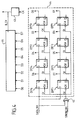
Selon ce mode de réalisation, des paquets de 8 bits provenant du système parallèle // sont reçus à un rythme fourni par une horloge B_CK, dite horloge paquet, et stockés dans un registre à 8 bits 22 dont les sorties D0 à D7 sont reliées à des moyens de décalage 23. Un circuit de synchronisation d'horloge 24 permet de recaler l'horloge paquet B_CK avec l'horloge interne CK dont la fréquence est multiple de l'horloge paquet B_CK, d'un facteur n (avec n=4 dans l'exemple de la figure 2). Les moyens de décalage 23 sont constitués de deux cascades de n registres à décalage en série alimentés respectivement avec les n bits pairs et les n bits impairs des données d'entrée à chaque nouvelle période de l'horloge paquet B_CK. Dans l'exemple de la figure 2, chaque cascade est constituée de 4 bascules D (qui recopient en sortie la valeur d'entrée sur un front d'horloge prédéterminé) connectées en série. A chaque nouvelle période de l'horloge paquet B_CK, les bascules de la cascade supérieure sont alimentées respectivement avec les 4 bits pairs disponibles sur D0 D2 D4 et D6, et celles de la cascade inférieure avec les 4 bits impairs sur D1 D3 D5 et D7. Chaque cascade de registres est active sur un front prédéterminé distinct de l'horloge interne CK pour transmettre séparément les bits pairs et impairs sur deux flux déphasés. Des moyens de comparaison 25 coopèrent avec les moyens de décalage 23 pour comparer les bits pairs et impairs consécutifs transmis par chaque cascade de bascules et pour en déduire le signal STROBE_TX. Ils comprennent :
- une paire de comparateurs de type ou exclusif XOR1 et XOR2 : XOR1 pour comparer les bits pairs et impairs consécutifs obtenus respectivement en sortie du dernier registre de la cascade supérieure DFF1 et en entrée du dernier registre de la cascade inférieure DFF2 et de façon symétrique, XOR2 pour comparer les bits pairs et impairs consécutifs respectivement en entrée du dernier registre de la cascade supérieure DFF1 et en sortie du dernier registre de la cascade inférieure DFF2,
- une paire d'inverseurs 26 et 27 pour inverser le signal en sortie des comparateurs XOR1 et XOR2,
- une paire de bascules de type JK configurées en bascules T (c'est-à-dire dont les entrées J et K sont reliées), dont l'une (JKF2) est reliée à la sortie du comparateur XOR1 via l'inverseur 26 et bascule sur le front descendant de l'horloge interne et l'autre (JKR2) est reliée à la sortie du comparateur XOR2 via l'inverseur 27 et bascule sur le front montant.
- a pair of XOR1 and XOR2 type or exclusive comparators: XOR1 to compare the consecutive even and odd bits obtained respectively at the output of the last register of the upper cascade DFF1 and at the input of the last register of the lower cascade DFF2 and symmetrically, XOR2 to compare the consecutive even and odd bits respectively at the input of the last register of the upper cascade DFF1 and at the output of the last register of the lower cascade DFF2,
- a pair of
inverters - a pair of flip-flops of type JK configured in flip-flops T (that is to say of which the inputs J and K are connected), one of which (JKF2) is connected to the output of the comparator XOR1 via the
inverter 26 and switches on the falling edge of the internal clock and the other (JKR2) is connected to the output of the comparator XOR2 via theinverter 27 and switches on the rising edge.
Des moyens de recalage temporel 28 sont également prévus pour retrouver les données d'entrée et en déduire le signal DATA_TX. Ils comportent une paire de bascules T JKF1 et JKR1 connectées en sortie des comparateurs XOR1 et XOR2 et reliées en entrée d'un comparateur de type ou exclusif XOR4 pour fournir le résultat DATA_TX.Time registration means 28 are also provided for retrieving the data input and deduce the DATA_TX signal. They include a pair of T flip-flops JKF1 and JKR1 connected at the output of comparators XOR1 and XOR2 and connected at the input of a comparator of type or exclusive XOR4 to provide the DATA_TX result.
Sur chaque front montant de l'horloge paquet B_CK, les 8 bits stockés dans le registre
sont disponibles sur les sorties D0 à D7 pour être envoyés en entrée des 8 bascules D, au signal
(SEL) du circuit de synchronisation d'horloge 24. Les bascules de la cascade supérieure reçoivent.
les bits pairs et sont activées sur les fronts montants de l'horloge interne dont la fréquence est
égale à 4 fois la fréquence de l'horloge paquet B_CK tandis que les bascules inférieures reçoivent
les bits impairs et sont activées sur les fronts descendants. Avant le prochain front descendant
de l'horloge interne CK, le comparateur XOR1 compare le bit N placé en entrée du dernier
registre (DFF2) de la rangée impaire au bit N-1 en sortie du dernier registre (DFF1) de la rangée
paire. Si les bits N et N-1 sont différents, cela signifie que le signal d'entrée a subi une transition.
Le signai de sortie du comparateur XOR1 vaudra 1 ce qui va provoquer le basculement de JKF1
et par conséquent, une transition sur le signal de sortie DATA_TX déclenchée par la transition de
la sortie du comparateur XOR4. La bascule JKF2 conserve la même valeur sur sa sortie grâce à
l'inverseur 26 placé à son entrée et donc le signal STROBE_TX reste inchangé. En revanche, si
les bits N et N-1 sont identiques, la bascule JKF1 conserve sa valeur de sortie et donc la valeur
du signal DATA_TX reste inchangée alors que la sortie de JKF2 bascule, provoquant ainsi une
transition sur le signal STROBE_TX. Après le front descendant de l'horloge interne CK, le bit N est
disponible en sortie du registre DFF2 pour permettre cette fois au comparateur XOR2 de
comparer le bit N au bit N+1 (toujours en entrée de DFF1) afin de mettre à jour la valeur des
signaux DATA_TX et STROBE_TX en sortie des comparateurs XOR4 et XOR3 lors du prochain
front montant.On each rising edge of the B_CK packet clock, the 8 bits stored in the register
are available on outputs D0 to D7 to be sent as input to the 8 D flip-flops, at the signal
(SEL) of the
Les différents signaux utilisés dans le dispositif de la figure 2 sont représentés sur un diagramme temporel à la figure 3. Il comprend :
- un signal D_IN(0...7) représentant les données du bus 8 bits en entrée du registre 22,
- un signal B_CK représentant le signal de l'horloge paquet,
- un signal SEL représentant le signal de sélection des bits en entrée des bascules D,
- un signal Q_IN(0...7) représentant les données D0 à D7 en sortie du registre 22,
- un signal CK représentant le signal de l'horloge interne,
- le signal DATA_TX et
- le signal STROBE_TX.
- a signal D_IN (0 ... 7) representing the data of the 8-bit bus at the input of
register 22, - a signal B_CK representing the signal of the packet clock,
- a signal SEL representing the signal for selecting the bits at the input of the D flip-flops,
- a signal Q_IN (0 ... 7) representing the data D0 to D7 at the output of
register 22, - a signal CK representing the signal from the internal clock,
- the DATA_TX signal and
- the STROBE_TX signal.
Les deux premiers octets seulement (0x80, 0x7F) fournis par le bus parallèle en entrée du
registre 8 bits 22 sont représentés sur le diagramme de la figure 3. Conformément à la
recommandation IEEE1394, les signaux DATA_TX et STROBE_TX n'ont jamais de transition au
même moment et le signal de l'horloge interne CK peut être obtenu par une opération de ou
exclusif entre les signaux DATA_TX et STROBE_TX.The first two bytes only (0x80, 0x7F) supplied by the parallel bus at the input of
8-
La figure 4 est un schéma bloc simplifié d'un dispositif d'interface selon l'invention pour convertir une paire de signaux d'entrée de type data et strobe notés DATA_RX et STROBE_RX en données de sortie formatées en paquets de 2n bits et notées D0 à D2n. Dans l'exemple de la figure 2n = 8. L'interface comprend:
un comparateur 42 pour comparer les signaux DATA_RX et STROBE_RX et pour obtenir en sortie un signal d'horloge interne CK permettant d'en déduire la fréquence binaire du signal DATA_RX,- un circuit générateur d'horloge 43 alimenté par l'horloge interne CK pour générer une horloge paquet, dite horloge de référence B_CK à une fréquence sous multiple de l'horloge interne, de facteur 1/n = 0.25,
- des moyens de décalage 44 comportant deux cascades de 4 registres à décalage en série
pour recevoir à chaque nouvelle période de l'horloge interne CK respectivement un nouveau
bit pair et un nouveau bit impair du signal DATA_RX, chaque cascade étant active sur un front
distinct prédéterminé de l'horloge interne CK pour transmettre séparément les bits pairs et
impairs sur deux flux série déphasés d'une demi période par rapport à l'horloge interne CK
(c'est-à-dire actifs sur un front distinct), et pour délivrer en sortie vers un registre 8
bits 46 les paquets de 8 bits à la fréquence de sortie déterminée par l'horloge paquet B_CK.
- a
comparator 42 for comparing the DATA_RX and STROBE_RX signals and for obtaining an internal clock signal CK at output making it possible to deduce therefrom the binary frequency of the signal DATA_RX, - a
clock generator circuit 43 supplied by the internal clock CK to generate a packet clock, called reference clock B_CK at a frequency under multiple of the internal clock, offactor 1 / n = 0.25, - shift means 44 comprising two cascades of 4 shift registers in series to receive each new period of the internal clock CK respectively a new even bit and a new odd bit of the DATA_RX signal, each cascade being active on a distinct predetermined edge of the internal clock CK to transmit the even and odd bits separately on two serial flows phase shifted by half a period with respect to the internal clock CK (i.e. active on a distinct edge), and to deliver as output to an 8-
bit register 46 the 8-bit packets at the output frequency determined by the packet clock B_CK.
La figure 5 illustre un premier exemple d'application de l'invention. Il s'agit de réaliser un
répéteur longue distance pour relier un câble utilisant le standard de communication IEEE1394 à
un support de transmission à fibre optique. Les signaux data et strobe transmis par le câble
IEEE1394 sont reçus par un port 51 via la paire TPA et TPB selon la norme IEEE1394. Les
signaux DATA_RX et STROBE_RX sont ensuite convertis en un flux d'octets à l'aide d'un dispositif
interface 52, par exemple du type de celui représenté à la figure 4. Le flux d'octets est alors codé
par un codeur 53 (par exemple de type 8B/10B ou 4B/5B) destiné à remplacer le paquet de 8
bits parallèles reçu du dispositif 52 par un paquet de 10 bits permettant par la suite au récepteur
situé à l'autre extrémité de la fibre optique de récupérer l'horloge du système. Le paquet de 10
bits est ensuite sérialisé (54) pour être envoyé sur la fibre optique 55 à l'aide d'un émetteur /
récepteur approprié 56. En sens inverse, le trafic de données provenant de la fibre optique est
dé-sérialisé (57) avant de subir un décodage 8B/10B (58) pour être ensuite converti en une paire
de signaux DATA_TX et STROBE_TX à destination du câble IEEE1394 à l'aide d'un dispositif
d'interface 59, par exemple du type de celui représenté à la figure 2.FIG. 5 illustrates a first example of application of the invention. This is to achieve a
long distance repeater to connect a cable using the IEEE1394 communication standard to
a fiber optic transmission medium. Data and strobe signals transmitted by cable
IEEE1394 are received by a
La figure 6 illustre un deuxième exemple d'application de l'invention pour implémenter une
interface entre la couche physique du bus IEEE1394 et un système hôte de traitement de
données CPU. L'interface peut être implémentée dans un circuit programmable à faible coût dont
la fréquence d'horloge de chaque composant ne dépasse pas N/2 MHz (où N est le débit binaire
des données transmises sur le bus IEEE1394 et vaut en général 100, 200 ou 400 Mbits/s). Les
signaux data et strobe sont reçus via un port spécifique 61 selon la recommandation IEEE1394.
Dans l'exemple de la figure 6 le circuit ne comporte qu'un seul port mais il peut en comporter
plusieurs en fonction des besoins de l'application. Le circuit d'interface comporte un dispositif 62
du type de celui représenté à la figure 4 pour convertir la paire de signaux DATA_RX et
STROBE_RX en un flux de données formatées en paquets d'octets et transmises via un bus
parallèle 63 vers une interface 64 du système de traitement de données CPU, contrôlée par un
organe de contrôle 65 qui reçoit, entre autres, les signaux DATA_RX et STROBE_RX. Il comporte
également un dispositif d'interface 67 du type de celui représenté à la figure 2 pour convertir le
flux parallèle de données formatées en paquets d'octets en une paire de signaux DATA_TX et
STROBE_TX vers le port IEEE1394 61.FIG. 6 illustrates a second example of application of the invention for implementing a
interface between the physical layer of the IEEE1394 bus and a host system for processing
CPU data. The interface can be implemented in a low cost programmable circuit including
the clock frequency of each component does not exceed N / 2 MHz (where N is the bit rate
data transmitted on the IEEE1394 bus and is generally 100, 200 or 400 Mbits / s). The
data and strobe signals are received via a
Un schéma général d'un système de transmission selon l'invention est représenté à la
figure 7. Il comporte un émetteur 71, un récepteur 72 et un canal de transmission 73 utilisant
par exemple une liaison par fibre optique, par paire torsadée ou tout autre medium câblé.
L'émetteur ou le récepteur peuvent notamment comporter des dispositifs d'interface du type de
ceux représentés aux figures 2 et 4 ou du type de celui de la figure 6 pour interfacer un système
parallèle, par exemple un organe de traitement de données à base de microprocesseur, et un
bus IEEE1394. Dans le cas d'une liaison optique entre un émetteur et un récepteur, le système
peut également être constitué d'un émetteur et d'un récepteur connectés à l'aide d'un câble
IEEE1394. Dans ce cas, le canal de transmission 73 peut être constitué par deux câbles
IEEE1394, l'un connecté à l'émetteur 71, l'autre au récepteur 72 et reliés entre eux via une liaison
optique connectée à chacun des câbles IEEE1394 par deux répéteurs du type de celui représenté
à la figure 5.A general diagram of a transmission system according to the invention is shown in the
Figure 7. It includes a
Claims (9)
caractérisé en ce qu'il comporte une interface pour convertir lesdits premier et deuxième signaux en données de sortie formatées en paquets de 2n bits, comprenant:
characterized in that it comprises an interface for converting said first and second signals into output data formatted in 2n bit packets, comprising:
caractérisé en ce que ladite interface comporte :
characterized in that said interface comprises:
caractérisé en ce qu'il comporte une interface pour convertir lesdits signaux en données de sortie formatées en paquets de 2n bits, comprenant :
characterized in that it comprises an interface for converting said signals into output data formatted in 2n bit packets, comprising:
caractérisé en ce que ladite interface comporte :
characterized in that said interface comprises:
caractérisé en ce qu'il comporte :
characterized in that it comprises:
caractérisé en ce que ladite interface comporte :
characterized in that said interface comprises:
caractérisé en ce qu'il comporte une interface pour convertir lesdits signaux en données de sortie formatées en paquets de 2n bits, comprenant :
characterized in that it comprises an interface for converting said signals into output data formatted in 2n bit packets, comprising:
Applications Claiming Priority (2)
| Application Number | Priority Date | Filing Date | Title |
|---|---|---|---|
| FR9907563A FR2795256A1 (en) | 1999-06-15 | 1999-06-15 | TRANSMISSION SYSTEM, RECEIVER, TRANSMITTER AND INTERFACE DEVICE FOR INTERFACING A PARALLEL SYSTEM WITH A DATA-STROBE TRANSCEIVER |
| FR9907563 | 1999-06-15 |
Publications (1)
| Publication Number | Publication Date |
|---|---|
| EP1061453A1 true EP1061453A1 (en) | 2000-12-20 |
Family
ID=9546817
Family Applications (1)
| Application Number | Title | Priority Date | Filing Date |
|---|---|---|---|
| EP00202011A Withdrawn EP1061453A1 (en) | 1999-06-15 | 2000-06-07 | Transmission system and interface and interface device between a parallel bus system and a transmitter/receiver |
Country Status (5)
| Country | Link |
|---|---|
| EP (1) | EP1061453A1 (en) |
| JP (1) | JP2001024712A (en) |
| KR (1) | KR20010015027A (en) |
| CN (1) | CN1278124A (en) |
| FR (1) | FR2795256A1 (en) |
Cited By (7)
| Publication number | Priority date | Publication date | Assignee | Title |
|---|---|---|---|---|
| EP1860815A1 (en) | 2006-05-24 | 2007-11-28 | High Tech Computer Corp. | Data transmission method and transmission circuit thereof |
| EP2040410A1 (en) | 2007-09-19 | 2009-03-25 | High Tech Computer Corp. | Data transmission method and system |
| US8266347B2 (en) | 2006-03-20 | 2012-09-11 | Htc Corporation | Data transmission method and transmission circuit thereof |
| US8687681B2 (en) | 2006-09-04 | 2014-04-01 | Via Technologies, Inc. | Receiver and signal testing method thereof |
| WO2014201293A1 (en) * | 2013-06-12 | 2014-12-18 | Qualcomm Incorporated | Camera control interface extension bus |
| WO2015195329A3 (en) * | 2014-06-18 | 2016-04-21 | Qualcomm Incorporated | Dynamically adjustable multi-line bus shared by multi-protocol devices |
| US10241955B2 (en) | 2014-06-18 | 2019-03-26 | Qualcomm Incorporated | Dynamically adjustable multi-line bus shared by multi-protocol devices |
Families Citing this family (3)
| Publication number | Priority date | Publication date | Assignee | Title |
|---|---|---|---|---|
| DE502007002941D1 (en) * | 2007-08-23 | 2010-04-08 | Siemens Ag | Method for data transmission |
| TWI581104B (en) * | 2016-05-11 | 2017-05-01 | 廣達電腦股份有限公司 | Host devices and methods for transmitting data |
| CN110958076B (en) * | 2018-09-26 | 2021-06-11 | 珠海格力电器股份有限公司 | Data transmission method and equipment |
Citations (2)
| Publication number | Priority date | Publication date | Assignee | Title |
|---|---|---|---|---|
| EP0631239A2 (en) * | 1993-05-14 | 1994-12-28 | Matsushita Electric Industrial Co., Ltd. | Serial data transfer method |
| US5479455A (en) * | 1993-06-30 | 1995-12-26 | Mitsubishi Denki Kabushiki Kaisha | Clock synchronous serial information transfer apparatus |
-
1999
- 1999-06-15 FR FR9907563A patent/FR2795256A1/en not_active Withdrawn
-
2000
- 2000-06-07 EP EP00202011A patent/EP1061453A1/en not_active Withdrawn
- 2000-06-12 CN CN00124129A patent/CN1278124A/en active Pending
- 2000-06-13 JP JP2000177208A patent/JP2001024712A/en active Pending
- 2000-06-15 KR KR1020000032947A patent/KR20010015027A/en not_active Application Discontinuation
Patent Citations (2)
| Publication number | Priority date | Publication date | Assignee | Title |
|---|---|---|---|---|
| EP0631239A2 (en) * | 1993-05-14 | 1994-12-28 | Matsushita Electric Industrial Co., Ltd. | Serial data transfer method |
| US5479455A (en) * | 1993-06-30 | 1995-12-26 | Mitsubishi Denki Kabushiki Kaisha | Clock synchronous serial information transfer apparatus |
Cited By (17)
| Publication number | Priority date | Publication date | Assignee | Title |
|---|---|---|---|---|
| US8266347B2 (en) | 2006-03-20 | 2012-09-11 | Htc Corporation | Data transmission method and transmission circuit thereof |
| EP1860815A1 (en) | 2006-05-24 | 2007-11-28 | High Tech Computer Corp. | Data transmission method and transmission circuit thereof |
| US8687681B2 (en) | 2006-09-04 | 2014-04-01 | Via Technologies, Inc. | Receiver and signal testing method thereof |
| EP2040410A1 (en) | 2007-09-19 | 2009-03-25 | High Tech Computer Corp. | Data transmission method and system |
| US9621334B2 (en) | 2007-09-19 | 2017-04-11 | Htc Corporation | Data transmission method and system |
| US9552325B2 (en) | 2013-06-12 | 2017-01-24 | Qualcomm Incorporated | Camera control interface extension bus |
| CN105283862A (en) * | 2013-06-12 | 2016-01-27 | 高通股份有限公司 | Camera control interface extension bus |
| WO2014201289A1 (en) * | 2013-06-12 | 2014-12-18 | Qualcomm Incorporated | Camera control interface extension bus |
| US9582457B2 (en) | 2013-06-12 | 2017-02-28 | Qualcomm Incorporated | Camera control interface extension bus |
| WO2014201293A1 (en) * | 2013-06-12 | 2014-12-18 | Qualcomm Incorporated | Camera control interface extension bus |
| US9639499B2 (en) | 2013-06-12 | 2017-05-02 | Qualcomm Incorporated | Camera control interface extension bus |
| US9811499B2 (en) | 2013-06-12 | 2017-11-07 | Qualcomm Incorporated | Transcoding and transmission over a serial bus |
| CN105283862B (en) * | 2013-06-12 | 2018-08-14 | 高通股份有限公司 | method and apparatus for data communication |
| WO2015195329A3 (en) * | 2014-06-18 | 2016-04-21 | Qualcomm Incorporated | Dynamically adjustable multi-line bus shared by multi-protocol devices |
| EP3236361A1 (en) * | 2014-06-18 | 2017-10-25 | Qualcomm Incorporated | Dynamically adjustable multi-line bus shared by multi-protocol devices |
| US10007628B2 (en) | 2014-06-18 | 2018-06-26 | Qualcomm Incorporated | Dynamically adjustable multi-line bus shared by multi-protocol devices |
| US10241955B2 (en) | 2014-06-18 | 2019-03-26 | Qualcomm Incorporated | Dynamically adjustable multi-line bus shared by multi-protocol devices |
Also Published As
| Publication number | Publication date |
|---|---|
| FR2795256A1 (en) | 2000-12-22 |
| JP2001024712A (en) | 2001-01-26 |
| CN1278124A (en) | 2000-12-27 |
| KR20010015027A (en) | 2001-02-26 |
Similar Documents
| Publication | Publication Date | Title |
|---|---|---|
| US20080019706A1 (en) | System and method for transmitting data on return path of a cable television system | |
| US7844181B2 (en) | Simple fibre channel speed negotiation across transport | |
| EP1061453A1 (en) | Transmission system and interface and interface device between a parallel bus system and a transmitter/receiver | |
| EP0187067B1 (en) | Switching system for a digital transmission network | |
| EP0407279A1 (en) | Communication network between user equipment | |
| EP0053958B1 (en) | Process for the parallel/series conversion of a digital parallel sequence | |
| EP2134026A1 (en) | Method for broadband data transmission and corresponding device(s) | |
| EP0108692B1 (en) | Method and installation for digital data transmission | |
| US6667994B1 (en) | Multiplexing digital communication system | |
| EP1401124A2 (en) | Optical subscriber network system for receiving broadcast/communication signals | |
| EP0120172B1 (en) | Bus interface device for a data processing system | |
| EP1445882B1 (en) | Data transmission frame and method and device for sending and receiving such a frame | |
| US5790057A (en) | Method of and system for the efficient encoding of data | |
| US8032916B2 (en) | Single master clock control of Ethernet data transfer over both a cable TV return path and an Ethernet forward path | |
| US7689128B2 (en) | Return path transmitter with extended digital processing circuitry | |
| EP0384795B1 (en) | Method and device for transmitting information between stations of a communication network, especially for a motor vehicle | |
| FR2534753A1 (en) | SYSTEM FOR ESTABLISHING DATA TRANSMISSION CIRCUITS AT CONSTANT FLOW BETWEEN A PLURALITY OF STATIONS | |
| FR2835377A1 (en) | COMMUNICATION SYSTEM COMPRISING MULTIPLE COMMUNICATION TERMINALS AND A SERVER, ITS COMMUNICATION TERMINAL, ITS SERVER AND THE DATA TRANSFER CONTROL PROGRAM | |
| EP0009557B1 (en) | Method and circuit for the simultaneous coding of two binary signal sequences into one pulse sequence, method and circuit for decoding the latter sequence, and their application to an interface transmitter-receiver | |
| FR2729262A1 (en) | DEVICE FOR INTERFACING COMMUNICATION MEDIA IN A DOMOTIC NETWORK | |
| EP1612985A1 (en) | Bidirectional communication | |
| FR2791206A1 (en) | METHOD FOR COMMUNICATING THE PARAMETERS OF A DIGITAL TRANSMISSION PROTOCOL | |
| FR2873532A1 (en) | METHOD FOR ENCODING AND DECODING A SEQUENCE OF ELEMENTS, SIGNAL, ENCODER, DECODER, COMPUTER PROGRAMS AND CORRESPONDING STORAGE MEANS | |
| FR2633473A1 (en) | METHOD OF RETRIEVING THE COMPONENT CONTINUING A DMAC-PACKET TYPE SIGNAL, DEVICE AND USE THEREOF | |
| EP1639785B1 (en) | Method for managing the redundancy of a communications network |
Legal Events
| Date | Code | Title | Description |
|---|---|---|---|
| PUAI | Public reference made under article 153(3) epc to a published international application that has entered the european phase |
Free format text: ORIGINAL CODE: 0009012 |
|
| AK | Designated contracting states |
Kind code of ref document: A1 Designated state(s): DE ES FR GB IT |
|
| AX | Request for extension of the european patent |
Free format text: AL;LT;LV;MK;RO;SI |
|
| 17P | Request for examination filed |
Effective date: 20010620 |
|
| AKX | Designation fees paid |
Free format text: DE ES FR GB IT |
|
| STAA | Information on the status of an ep patent application or granted ep patent |
Free format text: STATUS: THE APPLICATION HAS BEEN WITHDRAWN |
|
| 18W | Application withdrawn |
Withdrawal date: 20010926 |