EP1054401B1 - Detector error suppresion circuit and method - Google Patents
Detector error suppresion circuit and method Download PDFInfo
- Publication number
- EP1054401B1 EP1054401B1 EP00303986A EP00303986A EP1054401B1 EP 1054401 B1 EP1054401 B1 EP 1054401B1 EP 00303986 A EP00303986 A EP 00303986A EP 00303986 A EP00303986 A EP 00303986A EP 1054401 B1 EP1054401 B1 EP 1054401B1
- Authority
- EP
- European Patent Office
- Prior art keywords
- error
- encoding method
- bit
- epr4
- samples
- Prior art date
- Legal status (The legal status is an assumption and is not a legal conclusion. Google has not performed a legal analysis and makes no representation as to the accuracy of the status listed.)
- Expired - Lifetime
Links
Images


Classifications
-
- G—PHYSICS
- G11—INFORMATION STORAGE
- G11B—INFORMATION STORAGE BASED ON RELATIVE MOVEMENT BETWEEN RECORD CARRIER AND TRANSDUCER
- G11B20/00—Signal processing not specific to the method of recording or reproducing; Circuits therefor
- G11B20/10—Digital recording or reproducing
- G11B20/10009—Improvement or modification of read or write signals
- G11B20/10046—Improvement or modification of read or write signals filtering or equalising, e.g. setting the tap weights of an FIR filter
- G11B20/10055—Improvement or modification of read or write signals filtering or equalising, e.g. setting the tap weights of an FIR filter using partial response filtering when writing the signal to the medium or reading it therefrom
- G11B20/10064—EEPR4 or E2PR4, i.e. extended partial response class 4, polynomial (1-D)*(1+D)3
-
- G—PHYSICS
- G11—INFORMATION STORAGE
- G11B—INFORMATION STORAGE BASED ON RELATIVE MOVEMENT BETWEEN RECORD CARRIER AND TRANSDUCER
- G11B20/00—Signal processing not specific to the method of recording or reproducing; Circuits therefor
- G11B20/10—Digital recording or reproducing
- G11B20/10009—Improvement or modification of read or write signals
- G11B20/10046—Improvement or modification of read or write signals filtering or equalising, e.g. setting the tap weights of an FIR filter
- G11B20/10055—Improvement or modification of read or write signals filtering or equalising, e.g. setting the tap weights of an FIR filter using partial response filtering when writing the signal to the medium or reading it therefrom
- G11B20/10074—EPR4, i.e. extended partial response class 4, polynomial (1-D) *(1+D)2
-
- G—PHYSICS
- G11—INFORMATION STORAGE
- G11B—INFORMATION STORAGE BASED ON RELATIVE MOVEMENT BETWEEN RECORD CARRIER AND TRANSDUCER
- G11B20/00—Signal processing not specific to the method of recording or reproducing; Circuits therefor
- G11B20/10—Digital recording or reproducing
- G11B20/18—Error detection or correction; Testing, e.g. of drop-outs
- G11B20/1833—Error detection or correction; Testing, e.g. of drop-outs by adding special lists or symbols to the coded information
Definitions
- the invention relates to electronic devices, and, more particularly, but not exclusively, to digital communications and storage with partial response sequential detectors.
- Figure 1a schematically illustrates a magnetic storage and retrieval system.
- Error correction coder 101 encodes data bits into error corrected bits by an error correction encoding method such as Reed-Solomon. Further, the error correction coding may include interleaving of blocks of bits.
- modulation coder (channel coder) 103 codes blocks of bits output by error corrected coder 101 into blocks of bits using a runlength-limited code or other channel code which may include a parity bit for post processing removal of dominant errors. This modulation coding helps read timing recovery. These blocks may then be precoded. Then the (precoded) modulation coded bits drive the read/write head to set the magnetization orientation of domains on spinning magnetic disk 111; this stores the data bits.
- the reading of the stored data bits first amplifies (and filters) with amplifier 121 voltages induced in the read/write head 113 due to the transitions of magnetization orientation of domains on spinning disk 111.
- These voltages have the ideal form of a sequence of overlapping pulses, such as illustrated (after shape filtering) in Figures 2a-2c, with positive, negative, or zero amplitudes.
- the pulse overlaps imply intersymbol interference if the subsequent digital sampling includes contributions from more than one pulse; indeed, Figures 2a-2c indicate the ideal sampling times.
- Clocked analog-to-digital converter 123 samples and quantizes the sequence of pulses to form a digital output stream; there may be 64 or 128 quantization levels (a 6-bit or 7-bit converter with one sign bit and 5 or 6 magnitude bits).
- the Viterbi detector 125 performs a maximum likelihood data detection on the digital output stream.
- an (E)PR4 sensed voltage consists of a sequence of overlapping (E)PR4 pulses spaced one period apart and with positive, negative, or zero amplitudes depending upon the corresponding transitions of magnetization domain orientations.
- the sampling of the (E)PR4 sensed voltage yields the digital stream input to the detector, typically a sequence detector such as a maximum likelihood Viterbi decoder.
- a sequence detector such as a maximum likelihood Viterbi decoder.
- Higher storage densities on a magnetic disk require more samples per induced pulse and consequent more overlap, and thus the higher order polynomial transfer functions are used.
- storage densities of about 3 bits per PW50 (pulse width at half maximum amplitude) would use EEPR4 which has four nonzero samples per pulse; see Figure 2c.
- the demand for high density originates with small, portable devices such as notebook computers.
- Modulation decoder 127 is the inverse of modulation coder 103.
- error correction decoder 129 deinterleaves and further corrects errors and recovers the data bits, hopefully with only minimal errors.
- Maximum likelihood detection of a digital stream with intersymbol interference can be described in terms of maximizing probabilities of paths through a trellis of state transitions (branches); each state corresponds to a possible pattern of recently received data bits and each stage of the trellis corresponds to a receipt of the next (noisy) input.
- Figure 3 illustrates one stage (one step in time) in the trellis for an EPR4 detector; the states are labeled with three previous data bits (reflecting the three non-zero sampled values in the isolated pulse) and the branches are labeled 'with the bit for the branch transition plus the corresponding noiseless input sample target values: 2, 1, 0, -1, or -2.
- FIG. 4 shows a prior art Viterbi detector which includes one add-compare-select (ACS) unit for each trellis state and a branch metric unit for each of the target levels t ij ; the survival register for each state is in the path memories block.
- Each branch metric unit computes the square of the difference between its target value and the noisy input sample value.
- Each ACS stores a metric for its state and has inputs for the appropriate branch metric computations and the related state metrics from other ACS units.
- each ACS adds its (two) input branch metric computations to the corresponding state metrics of the states emitting the branches; and then it compares these (two) sums and selects the smaller as the updated state metric for its state.
- Each state's survival register updates its contents to maintain a survival path for the state; that is, the sequence of selected bits (transitions) that have led to the updated state metric.
- the detected bits will correspond to the path with the smallest metric.
- the maximum likelihood path through the trellis up to that time is the path traced backwards through the trellis starting from the state with the smallest state metric at that time and recursively using the branch previously selected as the branch into the traced-to state. That is, the survival register contents for the state with the smallest state metric.
- the length of the survival registers depends on the modulation code used. As the decision goes deeper into the survival registers, more of the contesting survival paths (versus the correct path) will be eliminated, the detected data will become more accurate.
- An error event metric may be defined as the difference between the path metric for the correct path and path metric for the contender error path through the trellis that diverges from the correct path and later remerges.
- the minimum squared Euclidean distance (metric) between paths equals 4.
- the first four errors have a common characteristic in that the error occurs when three or more consecutive transitions exist.
- a modulation code which prevents three consecutive transitions (NRZI tribits) will preclude the foregoing errors except for the single bit error.
- removing all tribits yields a low code rate. Consequently, various codes such as W.Bliss, An 8/9 Rate Time-Varying Trellis code for High Density Magnetic Recording, Proc. 1997 IEEE Int. Mag. Conf. (April 1997) remove quadbits and limit tribits to certain positions within the codeword to regain code rate.
- aspects of the present invention provide a device and method of single bit error suppression by post processing after Viterbi detection using a filtering of the difference of the ideal samples from the detected bit stream and the detector input sample stream.
- the first preferred embodiments suppress single bit errors in an EPR4 channel by post processing after the initial EPR4 Viterbi detection.
- Post processor 151 (details in Figures 1c-1d) filters the detected bit sequence, filters the sample sequence prior to detection, and then filters the difference of the two filtered sequences to assess the likelihood of a single bit error.
- the particular filterings provide single bit error detection with low-complexity by using EEPR4-type filters. If the comparison indicates a likely single bit error, then the output is corrected.
- Figure 1b is an overall preferred embodiment detector system block diagram showing an EEPR4-type filtering post processor 151 added onto an EPR4 system.
- This architecture allows post processor 151 to be added to a standard EPR4 system to improve the bit error rate (BER) performance without altering the EPR4 system.
- BER bit error rate
- Figure 1c is a block diagram of the first preferred embodiment post processor 151.
- the data path of the post processor can be broken down into two parts: the ideal data path and the sample data path.
- the ideal data path consists of four flip-flops, two multipliers (multiply by 2), and a four-input adder.
- Ideal EEPR4 samples have seven possible levels as compared to the five of ideal EPR4 samples.
- the EEPR4 transfer polynomial is (1-D)(1+D) 3 which can be expressed as (1-D)(1+D) 2 (1+D). And this is just the EPR4 transfer polynomial multiplied by (1+D).
- the samples input to the EPR4 Viterbi detector 125 can be converted into corresponding EEPR4 samples by filtering them with a 1+D filter.
- the samples input to the EPR4 Viterbi detector 125 are denoted as z[k]
- Figure 1c illustrates the ideal data path in the upper center and the sample data path in the lower left.
- the sample data path includes delay 153 to compensate for the delay through Viterbi detector 125 and thus synchronize with the ideal data path.
- the error event metric is then passed through error validation block 157 to identify the position of possible single bit errors. If the error event metric E[k] satisfies the following conditions, a flag will be sent to the error correction block 161 to invert the polarity of the k-5 output bit:
- a heuristic analysis will help clarify the operation of the foregoing preferred embodiment post processing.
- a common single bit error arises from pulse jitter in which the pulse induced in a read head is offset in time; this offset may be due to raggedness of the boundary of the magnetic domains of opposite polarities.
- the pulse offset combined with state metric variation within the Viterbi detector can lead to the single bit detection error.
- Figure 5 also shows the corresponding ideal correct samples and the ideal erroneous samples. That is, Figure 5 shows two ideal pulses and a delayed-by-jitter pulse in between the two ideal pulses.
- EEPR4 transfer function of -1, -2, 0, 2, 1 has such a shape and is convenient to use because EEPR4 hardware and software already exist.
- -1, -2, 0, 2, 1 filter to generate the E[k] sequence as 0, -1.2 ⁇ , -3.6 ⁇ - ⁇ 2 , -1.2 ⁇ -3 ⁇ 2 , 7.2 ⁇ -2 ⁇ 2 , 9.6 ⁇ +2 ⁇ 2 , 1.2 ⁇ +3 ⁇ 2 , -6 ⁇ + ⁇ 2 , -4.8 ⁇ , -1.2 ⁇ .
- the threshold of condition (2) being set equal to 5, and an error would be properly flagged by this E[k].
- the other terms of E[k] never exceed 4 in magnitude.
- the overall filtering from error bit to E[k] is (1-D)(1+D) 3 (1-D)(1+D) 3 which has coefficients 1,4,4,-4,-10,-4,4,4,1.
- the -10 coefficient has magnitude just twice the threshold, aligns with the dominate 9.6 ⁇ +2 ⁇ 2 + ⁇ term, and locates the error bit. Indeed, the magnitude of the -10 coefficient is more than twice that of the next largest magnitude coefficient.
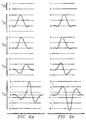
- Figures 6a-6b numerically illustrate the foregoing with z[k] taken as roughly equal to 0, 0.5, 1.8, 1.5, 0.5, 0, as in Figure 5. Indeed, with the correct bit sequence detected by Viterbi detector 125, the post processing would be as follows.
- the X C [k] sequence would be 0, 1, 1, 1, ...; the EEPR4 Y C [k] sequence 0, 1, 3, 3, 1, 0, 0; the error e C [k] sequence 0, -0.5, -0.7, 0.3, 1.0, 0.5, 0; and the error metric E C [k] sequence 0, -0.5, -1.7, -1.1, 0.6, 4.4, 1.1, 2.3, -2.0, -0.5 where (1+D)z[k] equal to 0, 0.5, 2.3, 3.3, 2.0, 0.5, 0, ... was used.
- Figure 6a illustrates these sequences and includes the ideal 0, 1, 2, 1, 0 EPR4 pulse for comparison.
- the post processing would be as follows. Using an E subscript for error, the X E [k] sequence would be 0, 0, 1, 1, 1, ...; the Y E [k] sequence 0, 0, 1, 3, 3, 1, 0; the e E [k] sequence 0, 0.5, 1.3, 0.3, -1.0, -0.5, 0; and the E E [k] sequence 0, 0.5, 2.3, 2.9, -0.4, -5.6, -2.9, 1.7, 2.0, 0.5.
- Figure 6b shows these sequences.
- Criteria (1) and (3) are met for E C [k] values -1.7, 4.4, and -2.3, and for E E [k] values 2.9, -5.6, and 2.0 (allowing 0 to be either sign).
- Setting the threshold at about 5 would correct the single bit error in that the error metric E C [k] for the correctly detected bit sequence does not set the error flag, but the error metric E E [k] for the incorrectly detected bit sequence does set the error flag.
- the samples z[k] could be compared to the ideal EPR4 samples and filtered by EPR4 to generate E[k].
- Figure 7 shows experimental results for the first preferred embodiment.
- the preferred embodiment post processor system shows a 1 dBN gain over a 16/17 code EPR4 system.
- the preferred embodiments can be modified in various ways while retaining the feature of a single bit error detection by comparison of the filtered difference between actual samples and ideal samples from the detected bit stream.
- the user bit density could be varied, the filtering to detect changed with corresponding changes in thresholds, and so forth.
- the computer program is stored on a carrier medium in machine or device readable form, for example in solid-state memory or magnetic memory such as disc or tape and the processing device utilises the program or a part thereof to configure it for operation.
- the computer program may be supplied from a remote source embodied in a communications medium such as an electronic signal, radio frequency carrier wave or optical carrier wave.
- a communications medium such as an electronic signal, radio frequency carrier wave or optical carrier wave.
- carrier media are also envisaged as aspects of the present invention.
Landscapes
- Engineering & Computer Science (AREA)
- Signal Processing (AREA)
- Physics & Mathematics (AREA)
- Algebra (AREA)
- Pure & Applied Mathematics (AREA)
- Signal Processing For Digital Recording And Reproducing (AREA)
- Error Detection And Correction (AREA)
- Detection And Correction Of Errors (AREA)
- Techniques For Improving Reliability Of Storages (AREA)
- Radar Systems Or Details Thereof (AREA)
- Detection And Prevention Of Errors In Transmission (AREA)
Abstract
Description
- The invention relates to electronic devices, and, more particularly, but not exclusively, to digital communications and storage with partial response sequential detectors.
- Figure 1a schematically illustrates a magnetic storage and retrieval system. In particular, writing data bits to storage on
magnetic disk 111 proceeds as follows.Error correction coder 101 encodes data bits into error corrected bits by an error correction encoding method such as Reed-Solomon. Further, the error correction coding may include interleaving of blocks of bits. Next, modulation coder (channel coder) 103 codes blocks of bits output by error correctedcoder 101 into blocks of bits using a runlength-limited code or other channel code which may include a parity bit for post processing removal of dominant errors. This modulation coding helps read timing recovery. These blocks may then be precoded. Then the (precoded) modulation coded bits drive the read/write head to set the magnetization orientation of domains on spinningmagnetic disk 111; this stores the data bits. - The reading of the stored data bits first amplifies (and filters) with
amplifier 121 voltages induced in the read/writehead 113 due to the transitions of magnetization orientation of domains on spinningdisk 111. These voltages have the ideal form of a sequence of overlapping pulses, such as illustrated (after shape filtering) in Figures 2a-2c, with positive, negative, or zero amplitudes. The pulse overlaps imply intersymbol interference if the subsequent digital sampling includes contributions from more than one pulse; indeed, Figures 2a-2c indicate the ideal sampling times. Clocked analog-to-digital converter 123 samples and quantizes the sequence of pulses to form a digital output stream; there may be 64 or 128 quantization levels (a 6-bit or 7-bit converter with one sign bit and 5 or 6 magnitude bits). The Viterbidetector 125 performs a maximum likelihood data detection on the digital output stream. - For partial response signaling various classes of frequency response for the signal channel prior to detection have been defined; and the class IV response appears particularly suitable for magnetic recording due to pulse shapes requiring minimal equalization. The partial response class IV channel is defined by a channel transfer function polynomial of the form (1-D)(1+D)N where N is a positive integer and D is a one period delay. Figures 2a-2c shows the pulse shapes for N = 1, 2, and 3; the corresponding pulses are termed PR4, EPR4, and E2PR4 (or EEPR4), respectively. Thus an (E)PR4 sensed voltage consists of a sequence of overlapping (E)PR4 pulses spaced one period apart and with positive, negative, or zero amplitudes depending upon the corresponding transitions of magnetization domain orientations. The sampling of the (E)PR4 sensed voltage yields the digital stream input to the detector, typically a sequence detector such as a maximum likelihood Viterbi decoder. Higher storage densities on a magnetic disk require more samples per induced pulse and consequent more overlap, and thus the higher order polynomial transfer functions are used. For example, storage densities of about 3 bits per PW50 (pulse width at half maximum amplitude) would use EEPR4 which has four nonzero samples per pulse; see Figure 2c. The demand for high density originates with small, portable devices such as notebook computers.
-
Modulation decoder 127 is the inverse ofmodulation coder 103. Lastly,error correction decoder 129 deinterleaves and further corrects errors and recovers the data bits, hopefully with only minimal errors. - Maximum likelihood detection of a digital stream with intersymbol interference can be described in terms of maximizing probabilities of paths through a trellis of state transitions (branches); each state corresponds to a possible pattern of recently received data bits and each stage of the trellis corresponds to a receipt of the next (noisy) input. For example, Figure 3 illustrates one stage (one step in time) in the trellis for an EPR4 detector; the states are labeled with three previous data bits (reflecting the three non-zero sampled values in the isolated pulse) and the branches are labeled 'with the bit for the branch transition plus the corresponding noiseless input sample target values: 2, 1, 0, -1, or -2.
- Figure 4 shows a prior art Viterbi detector which includes one add-compare-select (ACS) unit for each trellis state and a branch metric unit for each of the target levels tij; the survival register for each state is in the path memories block. Each branch metric unit computes the square of the difference between its target value and the noisy input sample value. Each ACS stores a metric for its state and has inputs for the appropriate branch metric computations and the related state metrics from other ACS units. At receipt of an input signal to the detector, each ACS adds its (two) input branch metric computations to the corresponding state metrics of the states emitting the branches; and then it compares these (two) sums and selects the smaller as the updated state metric for its state. Each state's survival register updates its contents to maintain a survival path for the state; that is, the sequence of selected bits (transitions) that have led to the updated state metric. The detected bits will correspond to the path with the smallest metric. At any time the maximum likelihood path through the trellis up to that time is the path traced backwards through the trellis starting from the state with the smallest state metric at that time and recursively using the branch previously selected as the branch into the traced-to state. That is, the survival register contents for the state with the smallest state metric.
- The length of the survival registers depends on the modulation code used. As the decision goes deeper into the survival registers, more of the contesting survival paths (versus the correct path) will be eliminated, the detected data will become more accurate.
- To further improve the performance of (E)PR4 channels, modulation codes have been proposed which add code constraints to eliminate the most common error events. An error event metric may be defined as the difference between the path metric for the correct path and path metric for the contender error path through the trellis that diverges from the correct path and later remerges. In EPR4 channels the minimum squared Euclidean distance (metric) between paths equals 4. The following pairs of bit sequences have trellis paths with this minimum error event metric:
00100 and 01010 (two consecutive transitions confused with four) 11011 and 10101 (complement of preceding) 01011 and 00101 (three consecutive transitions shifted) 10100 and 11010 (complement of preceding) xx0xx and xx1xx (single bit error) - The first four errors have a common characteristic in that the error occurs when three or more consecutive transitions exist. Thus a modulation code which prevents three consecutive transitions (NRZI tribits) will preclude the foregoing errors except for the single bit error. However, removing all tribits yields a low code rate. Consequently, various codes such as W.Bliss, An 8/9 Rate Time-Varying Trellis code for High Density Magnetic Recording, Proc. 1997 IEEE Int. Mag. Conf. (April 1997) remove quadbits and limit tribits to certain positions within the codeword to regain code rate.
- But the problem of suppression of single bit errors persists. One approach adds a parity bit to codewords, but this lowers the code rate.
- The document "PERD: Partial Error Response Detection", IEEE TRANSACTIONS ON MAGNETICS, vol. 31, no. 6, November 1995, pages 3042-3044, by T. NISHIYA AND H. YAMAKAWA discloses a PRML detector, wherein a PRML error waveform, defined as the difference between the actual sampled waveform ((1+D) filtered) and the waveform estimated from the PRML outputs, is compared with dominant error patterns. If the distance is small, the PRML bit stream is assumed to be in error and is corrected in accordance with the error pattern for which the distance is smallest.
- Aspects of the present invention provide a device and method of single bit error suppression by post processing after Viterbi detection using a filtering of the difference of the ideal samples from the detected bit stream and the detector input sample stream.
- This has the advantages of increased accuracy with limited additional post processing.
- Preferred embodiments of the invention will now be described, by way of example only, and with reference to the accompanying drawings, in which:
- The drawings are heuristic for clarity; and
- Figures 1a-1d schematically illustrates first preferred embodiment system.
- Figures 2a-2c shows partial response class IV pulses.
- Figure 3 illustrates a stage of an EPR4 trellis.
- Figure 4 shows a Viterbi detector.
- Figure 5 has EPR4 pulses.
- Figures 6a-6b illustrate post processing.
- Figure 7 is experimental results.
-
- As illustrated in Figures 1b-1d, the first preferred embodiments suppress single bit errors in an EPR4 channel by post processing after the initial EPR4 Viterbi detection. Post processor 151 (details in Figures 1c-1d) filters the detected bit sequence, filters the sample sequence prior to detection, and then filters the difference of the two filtered sequences to assess the likelihood of a single bit error. The particular filterings provide single bit error detection with low-complexity by using EEPR4-type filters. If the comparison indicates a likely single bit error, then the output is corrected.
- Figure 1b is an overall preferred embodiment detector system block diagram showing an EEPR4-type
filtering post processor 151 added onto an EPR4 system. Blocks before the post processor consist of a complete EPR4 system,post processor 151 works as an independent block: the only two inputs to postprocessor 151 are the 5-target-level (-2, -1, 0, 1, and 2) EPR4 sampled data and the detected bit stream output from the EPR4 Viterbi detector. This architecture allowspost processor 151 to be added to a standard EPR4 system to improve the bit error rate (BER) performance without altering the EPR4 system. - Figure 1c is a block diagram of the first preferred
embodiment post processor 151. The data path of the post processor can be broken down into two parts: the ideal data path and the sample data path. The ideal data path consists of four flip-flops, two multipliers (multiply by 2), and a four-input adder. The ideal data path filters the output bit stream X[k] of the EPR4 Viterbi detector (which is the maximum likelihood estimate of the bit stream initially recorded) with a filter that generates the ideal EEPR4 samples for such output bit stream:EPR4 Viterbi detector 125 can be converted into corresponding EEPR4 samples by filtering them with a 1+D filter. Thus if the samples input to theEPR4 Viterbi detector 125 are denoted as z[k], the sample data path outputs (1+D)z[k] = z[k] + z[k-1]. Figure 1c illustrates the ideal data path in the upper center and the sample data path in the lower left. The sample data path includesdelay 153 to compensate for the delay throughViterbi detector 125 and thus synchronize with the ideal data path. - The error signal at time k, e[k], is defined as the difference of the sample data path output and the ideal data path output; that is, e[k] = (1+D)z[k] - Y[k] = z[k] + z[k-1] - Y[k].
- Compute an error event metric E[k] by passing the error signal e[k] through a (1-D)(1+D)3 filter; that is, E[k] = (1-D)(1+D)3e[k] illustrated as
block 155 in Figure 1d. The error event metric is then passed througherror validation block 157 to identify the position of possible single bit errors. If the error event metric E[k] satisfies the following conditions, a flag will be sent to theerror correction block 161 to invert the polarity of the k-5 output bit: - (1) The error event metric E[k] has the same sign as the e[k] input to the error sequence filter.
- (2) The magnitude of error event metric E[k] is larger than a preset threshold.
- (3) The magnitude of error event metric E[k] is a local maximum (|E[k]| is larger than both |E[k-1]| and |E[k+1]|). Figure 1d illustrates circuitry for testing these conditions within
-
- A heuristic analysis will help clarify the operation of the foregoing preferred embodiment post processing. A common single bit error arises from pulse jitter in which the pulse induced in a read head is offset in time; this offset may be due to raggedness of the boundary of the magnetic domains of opposite polarities. The pulse offset combined with state metric variation within the Viterbi detector can lead to the single bit detection error. In particular, presume a correct bit sequence ...011..., an erroneous bit sequence of ...001..., and the samples z[k] as shown in Figure 5; Figure 5 also shows the corresponding ideal correct samples and the ideal erroneous samples. That is, Figure 5 shows two ideal pulses and a delayed-by-jitter pulse in between the two ideal pulses.
- As illustrated in Figure 5, if an ideal pulse with
samples - To emphasize the two successive 1.2δs (which correspond to the delay side of the correct pulse), filter with 1+D. This yields a filtered difference of 0, -1.28, -1.2δ-δ2, 1.2δ-δ2, 2.4δ, 1.2δ, 0 and corresponds to e[k].
- Then locate this pattern in e[k] by filtering with a filter having a transfer function of shape roughly equal to that of the pattern to be detected. The EEPR4 transfer function of -1, -2, 0, 2, 1 has such a shape and is convenient to use because EEPR4 hardware and software already exist. Thus apply the -1, -2, 0, 2, 1 filter to generate the E[k] sequence as 0, -1.2δ, -3.6δ-δ2, -1.2δ-3δ2, 7.2δ-2δ2, 9.6δ+2δ2, 1.2δ+3δ2, -6δ+δ2, -4.8δ, -1.2δ. Now as δ increases towards 0.5 (which implies the pulse is approaching an offset of one half sampling period and a high error probability), the 9.6δ+δ2 term will dominate and increase from 0 to about 5 as δ increases from 0 to 0.5. This suggests a threshold about 5 for use as condition (2) in the preferred embodiment error decision.
- A similar analysis for the difference between the jittered pulse samples and the ideal erroneous samples (which equals 0, 1-1.2δ, 1-δ2, -1+1.2δ, -1+1.2δ) yields E[k] as 0, 1-1.2δ, 4-3.6δ-δ2, 4-1.2δ-3δ2, -4+7.2δ-2δ2, -10+9.6δ+2δ2, -4+1.2δ+3δ2, 4-6δ+δ2, 4-4.8δ, 1-1.2δ. Of course, this difference equals the correct bit samples difference plus the error bit samples. The term -10+9.6δ+2δ2 dominates and its magnitude decreases from 10 to about 5 as δ increases from 0 to 0.5. This agrees with the threshold of condition (2) being set equal to 5, and an error would be properly flagged by this E[k]. Note that the other terms of E[k] never exceed 4 in magnitude. Also, the overall filtering from error bit to E[k] is (1-D)(1+D)3(1-D)(1+D)3 which has
coefficients - Figures 6a-6b numerically illustrate the foregoing with z[k] taken as roughly equal to 0, 0.5, 1.8, 1.5, 0.5, 0, as in Figure 5. Indeed, with the correct bit sequence detected by
Viterbi detector 125, the post processing would be as follows. Using a subscript C for correct, the XC[k] sequence would be 0, 1, 1, 1, ...; the EEPR4 YC[k]sequence sequence 0, -0.5, -0.7, 0.3, 1.0, 0.5, 0; and the error metric EC[k]sequence 0, -0.5, -1.7, -1.1, 0.6, 4.4, 1.1, 2.3, -2.0, -0.5 where (1+D)z[k] equal to 0, 0.5, 2.3, 3.3, 2.0, 0.5, 0, ... was used. Figure 6a illustrates these sequences and includes the ideal 0, 1, 2, 1, 0 EPR4 pulse for comparison. - Conversely, if the erroneous bit sequence is detected by Viterbi detector 125 (due to, for example, differences in previously accumulated fluctuations in state metrics), then the post processing would be as follows. Using an E subscript for error, the XE[k] sequence would be 0, 0, 1, 1, 1, ...; the YE[k]
sequence sequence 0, 0.5, 1.3, 0.3, -1.0, -0.5, 0; and the EE[k]sequence 0, 0.5, 2.3, 2.9, -0.4, -5.6, -2.9, 1.7, 2.0, 0.5. Figure 6b shows these sequences. - Consider the criteria for setting the error flag and inverting the output bit:
- (1) e[k] and E[k] have the same sign.
- (2) E[k] exceeds a threshold.
- (3) |E[k]| is a local maximum.
-
- Criteria (1) and (3) are met for EC[k] values -1.7, 4.4, and -2.3, and for EE[k] values 2.9, -5.6, and 2.0 (allowing 0 to be either sign). Thus setting the threshold at about 5 would correct the single bit error in that the error metric EC[k] for the correctly detected bit sequence does not set the error flag, but the error metric EE[k] for the incorrectly detected bit sequence does set the error flag.
- Other filterings of e[k] could be used in place of the EEPR4 filter of -1, -2, 0, 2, 1 to detect the basic pattern of e[k] which has the dominate positive term (i.e., 2.4δ) two samples after the dominate negative term (i.e., -1.2δ-δ2). Thus a filter such as -1, 0, 1 would still fit the pattern: in this case E[k] sequence would become 0, -1.2δ, -1.2δ-δ2, 2.4δ-δ2, 3.6δ+δ2, δ2, -2.4δ, -1.2δ. Thus as δ increases from 0 to 0.5, the dominate term (3.6δ+δ2) will approach about 2, so a threshold about 2 should be used. This agrees with the overall filtering of the error bit as (1-D)(1+D)3(1-D2) which has
coefficients - Note that for this -1, 0, 1 filter the ratio of the dominate term to the next largest term is (3.6δ+δ2)/(-2.4δ) = -1.7 as δ increases to 0.5. This matches the ratio for the -1,-2,0,2,1 filter of (9.6δ+2δ2)/(7.2δ-2δ2) = 1.7 as δ increases to 0.5.
- Alternatively, the samples z[k] could be compared to the ideal EPR4 samples and filtered by EPR4 to generate E[k]. In this case the overall error bit filtering is (1-D)(1+D)2(1-D)(1+D)2 which is just a rearrangement of the preceding: (1-D)(1+D)2(1-D)(1+D)2 = (1-D)(1+D)3(1-D2).
- Figure 7 shows experimental results for the first preferred embodiment. By removing the single bit errors from the output using post processing and removing the consecutive transition errors with trellis coding, at user density of 3.0 the preferred embodiment post processor system shows a 1 dBN gain over a 16/17 code EPR4 system.
- The preferred embodiments can be modified in various ways while retaining the feature of a single bit error detection by comparison of the filtered difference between actual samples and ideal samples from the detected bit stream. For example, the user bit density could be varied, the filtering to detect changed with corresponding changes in thresholds, and so forth.
- Insofar as embodiments of the invention described above are implementable, at least in part, using a software-controlled programmable processing device such as a Digital Signal Processor, microprocessor or other processing device, it will be appreciated that a computer program for configuring the programmable device to implement the foregoing described methods is envisaged as an aspect of the present invention.
- Suitably, the computer program is stored on a carrier medium in machine or device readable form, for example in solid-state memory or magnetic memory such as disc or tape and the processing device utilises the program or a part thereof to configure it for operation. The computer program may be supplied from a remote source embodied in a communications medium such as an electronic signal, radio frequency carrier wave or optical carrier wave. Such carrier media are also envisaged as aspects of the present invention.
Claims (6)
- A method of correcting errors, comprising:(a) estimating information from a first sample stream which encodes information with a first encoding method;(b) comparing the difference between (i) said sample stream after a first filtering and (ii) an ideal sample stream created from said estimated information with a second encoding method, wherein said second encoding method emulates said first encoding method plus said first filtering; and(c) correcting said estimated information of (a) when said comparison of (b) indicates an error.
- The method of claim 1, wherein:(a) said first encoding method is EPR4; and(b) said second encoding method is EEPR4.
- A computer program comprising computer program means for configuring a processing device in accordance with claim 1 or 2.
- A computer program carrier medium carrying a computer program according to claim 3.
- A processing device configured in accordance with a computer program according to claim 3.
- A circuit for correcting errors, comprising:means (125) for estimating information from a first sample stream which encodes information with a first encoding method;means (155, 157) for comparing the difference between (i) said sample stream after a first filtering and (ii) an ideal sample stream created from said estimated information with a second encoding method, said second encoding method emulating said first encoding method plus said first filtering; andmeans (161) for correcting said estimated information when said means for comparing indicates an error.
Applications Claiming Priority (2)
| Application Number | Priority Date | Filing Date | Title |
|---|---|---|---|
| US13490999P | 1999-05-19 | 1999-05-19 | |
| US134909P | 1999-05-19 |
Publications (3)
| Publication Number | Publication Date |
|---|---|
| EP1054401A2 EP1054401A2 (en) | 2000-11-22 |
| EP1054401A3 EP1054401A3 (en) | 2001-09-05 |
| EP1054401B1 true EP1054401B1 (en) | 2004-03-03 |
Family
ID=22465562
Family Applications (1)
| Application Number | Title | Priority Date | Filing Date |
|---|---|---|---|
| EP00303986A Expired - Lifetime EP1054401B1 (en) | 1999-05-19 | 2000-05-11 | Detector error suppresion circuit and method |
Country Status (6)
| Country | Link |
|---|---|
| US (1) | US6546518B1 (en) |
| EP (1) | EP1054401B1 (en) |
| JP (1) | JP2001024519A (en) |
| AT (1) | ATE261175T1 (en) |
| DE (1) | DE60008624T2 (en) |
| TW (1) | TW493165B (en) |
Families Citing this family (12)
| Publication number | Priority date | Publication date | Assignee | Title |
|---|---|---|---|---|
| JP2001266499A (en) * | 2000-03-23 | 2001-09-28 | Sony Corp | Unit and method for recording data, device and method for reproducing data, unit and method for recording and reproducing data |
| JP4555454B2 (en) * | 2000-11-21 | 2010-09-29 | 富士通株式会社 | Data playback device |
| EP1271509A1 (en) * | 2001-06-22 | 2003-01-02 | STMicroelectronics S.r.l. | Method and apparatus for detecting and correcting errors in a magnetic recording channel of a mass storage system |
| WO2003012789A1 (en) * | 2001-07-27 | 2003-02-13 | Fujitsu Limited | Signal processing method, signal processing circuit and information recorder/reproducer |
| US7184237B2 (en) * | 2001-08-21 | 2007-02-27 | Seagate Technology Llc | Method and apparatus for selecting equalization targets |
| EP1508813B1 (en) * | 2003-08-20 | 2007-01-31 | Agilent Technologies, Inc. | Spectral jitter analysis allowing jitter modulation waveform analysis |
| US7173784B2 (en) * | 2003-10-10 | 2007-02-06 | Hitachi Global Storage Technologies Netherlands B.V. | Apparatus for providing data dependent detection in a data read channel |
| JP4622632B2 (en) * | 2005-03-31 | 2011-02-02 | ソニー株式会社 | Maximum likelihood decoding apparatus, signal evaluation method, reproduction apparatus |
| US8145983B1 (en) * | 2006-11-08 | 2012-03-27 | Marvell International Ltd. | Methods and apparatus for identification of likely errors in data blocks |
| JP2009110572A (en) * | 2007-10-29 | 2009-05-21 | Funai Electric Co Ltd | Optical disk recording and playback device |
| US7755521B1 (en) | 2008-12-23 | 2010-07-13 | Advantest Corporation | A-D convert apparatus, D-A convert apparatus and adjustment method |
| JP2020135391A (en) | 2019-02-19 | 2020-08-31 | キオクシア株式会社 | Memory system |
Family Cites Families (9)
| Publication number | Priority date | Publication date | Assignee | Title |
|---|---|---|---|---|
| JPH0877726A (en) * | 1994-09-06 | 1996-03-22 | Hitachi Ltd | Digital signal processing device, error detecting method and recording medium reproducing device |
| JPH08329619A (en) * | 1994-10-27 | 1996-12-13 | Hitachi Ltd | Method and device for producing data and data reproducing circuit |
| US5521945A (en) | 1995-06-30 | 1996-05-28 | Quantum Corporation | Reduced complexity EPR4 post-processor for sampled data detection |
| US5938790A (en) * | 1997-03-04 | 1999-08-17 | Silicon Systems Research Ltd. | Sequence error event detection and correction using fixed block digital sum codes |
| US5949831A (en) | 1997-05-21 | 1999-09-07 | International Business Machines Corporation | Method and apparatus for data detection for PRML data channels |
| US5961658A (en) * | 1997-05-23 | 1999-10-05 | Cirrus Logic, Inc. | PR4 equalization and an EPR4 remod/demod sequence detector in a sampled amplitude read channel |
| US6052248A (en) * | 1998-01-30 | 2000-04-18 | Cirrus Logic, Inc. | Parity channel code for enhancing the operation of a remod/demod sequence detector in a d=1 sampled amplitude read channel |
| US6185173B1 (en) | 1998-07-31 | 2001-02-06 | Cirrus Logic, Inc. | Sampled amplitude read channel employing a trellis sequence detector matched to a channel code constraint and a post processor for correcting errors in the detected binary sequence using the signal samples and an error syndrome |
| US6185175B1 (en) * | 1998-12-02 | 2001-02-06 | Cirrus Logic, Inc. | Sampled amplitude read channel employing noise whitening in a remod/demod sequence detector |
-
2000
- 2000-04-14 US US09/549,458 patent/US6546518B1/en not_active Expired - Lifetime
- 2000-05-11 EP EP00303986A patent/EP1054401B1/en not_active Expired - Lifetime
- 2000-05-11 AT AT00303986T patent/ATE261175T1/en not_active IP Right Cessation
- 2000-05-11 DE DE60008624T patent/DE60008624T2/en not_active Expired - Lifetime
- 2000-05-18 JP JP2000146722A patent/JP2001024519A/en not_active Abandoned
- 2000-05-19 TW TW089109682A patent/TW493165B/en not_active IP Right Cessation
Also Published As
| Publication number | Publication date |
|---|---|
| JP2001024519A (en) | 2001-01-26 |
| EP1054401A3 (en) | 2001-09-05 |
| DE60008624T2 (en) | 2005-02-03 |
| TW493165B (en) | 2002-07-01 |
| EP1054401A2 (en) | 2000-11-22 |
| DE60008624D1 (en) | 2004-04-08 |
| ATE261175T1 (en) | 2004-03-15 |
| US6546518B1 (en) | 2003-04-08 |
Similar Documents
| Publication | Publication Date | Title |
|---|---|---|
| EP0369962B1 (en) | Method for processing signals in a channel | |
| US5689532A (en) | Reduced complexity EPR4 post-processor for sampled data detection | |
| US6023386A (en) | Fault tolerant sync mark detector for synchronizing a time varying sequence detector in a sampled amplitude read channel | |
| US6246723B1 (en) | Sampled amplitude read channel employing early-decisions from a trellis sequence detector for sampling value estimation | |
| US7089483B2 (en) | Two stage detector having viterbi detector matched to a channel and post processor matched to a channel code | |
| US6185173B1 (en) | Sampled amplitude read channel employing a trellis sequence detector matched to a channel code constraint and a post processor for correcting errors in the detected binary sequence using the signal samples and an error syndrome | |
| US6460150B1 (en) | Noise-predictive post-processing for PRML data channel | |
| GB2286952A (en) | Maximum-likelihood data detection in a partial-response data channel for a direct access storage device | |
| US6154870A (en) | Signal error-correction system and method | |
| EP1054401B1 (en) | Detector error suppresion circuit and method | |
| US6307884B1 (en) | Dual decision feedback equalizer with selective attenuation to improve channel performance | |
| US5844507A (en) | Rate 16/17 ENDEC with independent high/low byte decoding | |
| US6366418B1 (en) | Method for reducing data overhead in PRML data channel | |
| US6735724B1 (en) | Detection error estimation and method | |
| US6282690B1 (en) | Parity insertion with precoder feedback in a read channel | |
| US5949357A (en) | Time-varying maximum-transition-run codes for data channels | |
| US5838738A (en) | Coding to improve timing recovery in a sampled amplitude read channel | |
| US5931966A (en) | Viterbi detector with a pipelined look-up table of squared errors | |
| JP3950579B2 (en) | Encoding method and recording / reproducing apparatus using the same | |
| US5786950A (en) | PR4 sampled amplitude read channel employing an NRZI write modulator and a PR4/NRZI converter | |
| WO1999017456A9 (en) | Method and apparatus for encoding a binary signal | |
| WO2000017872A1 (en) | Generation of amplitude levels for a partial response maximum likelihood (prml) bit detector | |
| EP1081868A2 (en) | Supporting an E2PRML-type channel and an EPRML-type channel with the same trellis structure | |
| US6393598B1 (en) | Branch metric compensation for digital sequence detection | |
| US6704903B1 (en) | Simplified branch metric and method |
Legal Events
| Date | Code | Title | Description |
|---|---|---|---|
| PUAI | Public reference made under article 153(3) epc to a published international application that has entered the european phase |
Free format text: ORIGINAL CODE: 0009012 |
|
| AK | Designated contracting states |
Kind code of ref document: A2 Designated state(s): AT BE CH CY DE DK ES FI FR GB GR IE IT LI LU MC NL PT SE |
|
| AX | Request for extension of the european patent |
Free format text: AL;LT;LV;MK;RO;SI |
|
| PUAL | Search report despatched |
Free format text: ORIGINAL CODE: 0009013 |
|
| AK | Designated contracting states |
Kind code of ref document: A3 Designated state(s): AT BE CH CY DE DK ES FI FR GB GR IE IT LI LU MC NL PT SE |
|
| AX | Request for extension of the european patent |
Free format text: AL;LT;LV;MK;RO;SI |
|
| 17P | Request for examination filed |
Effective date: 20020226 |
|
| AKX | Designation fees paid |
Free format text: AT BE CH CY DE DK ES FI FR GB GR IE IT LI LU MC NL PT SE |
|
| 17Q | First examination report despatched |
Effective date: 20020510 |
|
| GRAP | Despatch of communication of intention to grant a patent |
Free format text: ORIGINAL CODE: EPIDOSNIGR1 |
|
| RBV | Designated contracting states (corrected) |
Designated state(s): DE FR GB IT NL |
|
| GRAS | Grant fee paid |
Free format text: ORIGINAL CODE: EPIDOSNIGR3 |
|
| GRAA | (expected) grant |
Free format text: ORIGINAL CODE: 0009210 |
|
| RBV | Designated contracting states (corrected) |
Designated state(s): AT BE CH CY DE DK ES FI FR GB GR IE IT LI LU MC NL PT SE |
|
| AK | Designated contracting states |
Kind code of ref document: B1 Designated state(s): AT BE CH CY DE DK ES FI FR GB GR IE IT LI LU MC NL PT SE |
|
| PG25 | Lapsed in a contracting state [announced via postgrant information from national office to epo] |
Ref country code: IT Free format text: LAPSE BECAUSE OF FAILURE TO SUBMIT A TRANSLATION OF THE DESCRIPTION OR TO PAY THE FEE WITHIN THE PRESCRIBED TIME-LIMIT;WARNING: LAPSES OF ITALIAN PATENTS WITH EFFECTIVE DATE BEFORE 2007 MAY HAVE OCCURRED AT ANY TIME BEFORE 2007. THE CORRECT EFFECTIVE DATE MAY BE DIFFERENT FROM THE ONE RECORDED. Effective date: 20040303 Ref country code: CY Free format text: LAPSE BECAUSE OF FAILURE TO SUBMIT A TRANSLATION OF THE DESCRIPTION OR TO PAY THE FEE WITHIN THE PRESCRIBED TIME-LIMIT Effective date: 20040303 Ref country code: NL Free format text: LAPSE BECAUSE OF FAILURE TO SUBMIT A TRANSLATION OF THE DESCRIPTION OR TO PAY THE FEE WITHIN THE PRESCRIBED TIME-LIMIT Effective date: 20040303 Ref country code: AT Free format text: LAPSE BECAUSE OF FAILURE TO SUBMIT A TRANSLATION OF THE DESCRIPTION OR TO PAY THE FEE WITHIN THE PRESCRIBED TIME-LIMIT Effective date: 20040303 Ref country code: BE Free format text: LAPSE BECAUSE OF FAILURE TO SUBMIT A TRANSLATION OF THE DESCRIPTION OR TO PAY THE FEE WITHIN THE PRESCRIBED TIME-LIMIT Effective date: 20040303 Ref country code: CH Free format text: LAPSE BECAUSE OF FAILURE TO SUBMIT A TRANSLATION OF THE DESCRIPTION OR TO PAY THE FEE WITHIN THE PRESCRIBED TIME-LIMIT Effective date: 20040303 Ref country code: LI Free format text: LAPSE BECAUSE OF FAILURE TO SUBMIT A TRANSLATION OF THE DESCRIPTION OR TO PAY THE FEE WITHIN THE PRESCRIBED TIME-LIMIT Effective date: 20040303 |
|
| REG | Reference to a national code |
Ref country code: GB Ref legal event code: FG4D |
|
| REG | Reference to a national code |
Ref country code: CH Ref legal event code: EP |
|
| REG | Reference to a national code |
Ref country code: IE Ref legal event code: FG4D |
|
| REF | Corresponds to: |
Ref document number: 60008624 Country of ref document: DE Date of ref document: 20040408 Kind code of ref document: P |
|
| PG25 | Lapsed in a contracting state [announced via postgrant information from national office to epo] |
Ref country code: LU Free format text: LAPSE BECAUSE OF NON-PAYMENT OF DUE FEES Effective date: 20040511 Ref country code: IE Free format text: LAPSE BECAUSE OF NON-PAYMENT OF DUE FEES Effective date: 20040511 |
|
| PG25 | Lapsed in a contracting state [announced via postgrant information from national office to epo] |
Ref country code: FI Free format text: LAPSE BECAUSE OF NON-PAYMENT OF DUE FEES Effective date: 20040531 Ref country code: MC Free format text: LAPSE BECAUSE OF NON-PAYMENT OF DUE FEES Effective date: 20040531 |
|
| PG25 | Lapsed in a contracting state [announced via postgrant information from national office to epo] |
Ref country code: SE Free format text: LAPSE BECAUSE OF FAILURE TO SUBMIT A TRANSLATION OF THE DESCRIPTION OR TO PAY THE FEE WITHIN THE PRESCRIBED TIME-LIMIT Effective date: 20040603 Ref country code: DK Free format text: LAPSE BECAUSE OF FAILURE TO SUBMIT A TRANSLATION OF THE DESCRIPTION OR TO PAY THE FEE WITHIN THE PRESCRIBED TIME-LIMIT Effective date: 20040603 Ref country code: GR Free format text: LAPSE BECAUSE OF FAILURE TO SUBMIT A TRANSLATION OF THE DESCRIPTION OR TO PAY THE FEE WITHIN THE PRESCRIBED TIME-LIMIT Effective date: 20040603 |
|
| PG25 | Lapsed in a contracting state [announced via postgrant information from national office to epo] |
Ref country code: ES Free format text: LAPSE BECAUSE OF FAILURE TO SUBMIT A TRANSLATION OF THE DESCRIPTION OR TO PAY THE FEE WITHIN THE PRESCRIBED TIME-LIMIT Effective date: 20040614 |
|
| NLV1 | Nl: lapsed or annulled due to failure to fulfill the requirements of art. 29p and 29m of the patents act | ||
| REG | Reference to a national code |
Ref country code: CH Ref legal event code: PL |
|
| ET | Fr: translation filed | ||
| PLBE | No opposition filed within time limit |
Free format text: ORIGINAL CODE: 0009261 |
|
| STAA | Information on the status of an ep patent application or granted ep patent |
Free format text: STATUS: NO OPPOSITION FILED WITHIN TIME LIMIT |
|
| REG | Reference to a national code |
Ref country code: IE Ref legal event code: MM4A |
|
| 26N | No opposition filed |
Effective date: 20041206 |
|
| PG25 | Lapsed in a contracting state [announced via postgrant information from national office to epo] |
Ref country code: PT Free format text: LAPSE BECAUSE OF NON-PAYMENT OF DUE FEES Effective date: 20040803 |
|
| REG | Reference to a national code |
Ref country code: FR Ref legal event code: PLFP Year of fee payment: 16 |
|
| PGFP | Annual fee paid to national office [announced via postgrant information from national office to epo] |
Ref country code: DE Payment date: 20150601 Year of fee payment: 16 Ref country code: GB Payment date: 20150424 Year of fee payment: 16 |
|
| PGFP | Annual fee paid to national office [announced via postgrant information from national office to epo] |
Ref country code: FR Payment date: 20150424 Year of fee payment: 16 |
|
| REG | Reference to a national code |
Ref country code: DE Ref legal event code: R119 Ref document number: 60008624 Country of ref document: DE |
|
| GBPC | Gb: european patent ceased through non-payment of renewal fee |
Effective date: 20160511 |
|
| REG | Reference to a national code |
Ref country code: FR Ref legal event code: ST Effective date: 20170131 |
|
| PG25 | Lapsed in a contracting state [announced via postgrant information from national office to epo] |
Ref country code: FR Free format text: LAPSE BECAUSE OF NON-PAYMENT OF DUE FEES Effective date: 20160531 Ref country code: DE Free format text: LAPSE BECAUSE OF NON-PAYMENT OF DUE FEES Effective date: 20161201 |
|
| PG25 | Lapsed in a contracting state [announced via postgrant information from national office to epo] |
Ref country code: GB Free format text: LAPSE BECAUSE OF NON-PAYMENT OF DUE FEES Effective date: 20160511 |