EP1052794B1 - Protocol independent sub-rate device - Google Patents
Protocol independent sub-rate device Download PDFInfo
- Publication number
- EP1052794B1 EP1052794B1 EP00303925A EP00303925A EP1052794B1 EP 1052794 B1 EP1052794 B1 EP 1052794B1 EP 00303925 A EP00303925 A EP 00303925A EP 00303925 A EP00303925 A EP 00303925A EP 1052794 B1 EP1052794 B1 EP 1052794B1
- Authority
- EP
- European Patent Office
- Prior art keywords
- data information
- data
- buffering
- devices
- multiplexer according
- Prior art date
- Legal status (The legal status is an assumption and is not a legal conclusion. Google has not performed a legal analysis and makes no representation as to the accuracy of the status listed.)
- Expired - Lifetime
Links
Images


Classifications
-
- H—ELECTRICITY
- H04—ELECTRIC COMMUNICATION TECHNIQUE
- H04J—MULTIPLEX COMMUNICATION
- H04J3/00—Time-division multiplex systems
- H04J3/16—Time-division multiplex systems in which the time allocation to individual channels within a transmission cycle is variable, e.g. to accommodate varying complexity of signals, to vary number of channels transmitted
- H04J3/1605—Fixed allocated frame structures
- H04J3/1611—Synchronous digital hierarchy [SDH] or SONET
-
- H—ELECTRICITY
- H04—ELECTRIC COMMUNICATION TECHNIQUE
- H04J—MULTIPLEX COMMUNICATION
- H04J3/00—Time-division multiplex systems
- H04J3/16—Time-division multiplex systems in which the time allocation to individual channels within a transmission cycle is variable, e.g. to accommodate varying complexity of signals, to vary number of channels transmitted
- H04J3/1682—Allocation of channels according to the instantaneous demands of the users, e.g. concentrated multiplexers, statistical multiplexers
-
- H—ELECTRICITY
- H04—ELECTRIC COMMUNICATION TECHNIQUE
- H04J—MULTIPLEX COMMUNICATION
- H04J3/00—Time-division multiplex systems
- H04J3/22—Time-division multiplex systems in which the sources have different rates or codes
Landscapes
- Engineering & Computer Science (AREA)
- Computer Networks & Wireless Communication (AREA)
- Signal Processing (AREA)
- Multimedia (AREA)
- Time-Division Multiplex Systems (AREA)
- Communication Control (AREA)
- Data Exchanges In Wide-Area Networks (AREA)
Description
- The present invention relates generally to interface devices within communication systems and more specifically to devices such as multiplexers and demultiplexers implemented within communication systems such as optical fiber communication systems.
- An integral part of any communication system is the protocol that is utilized to properly transmit the desired information from a first location to a second location. As an increasing amount of information is transmitted through optical fiber communication systems, numerous standard protocols have been established and more are currently being defined. These protocols utilize different rates and formats in order to balance the advantages of increased flexibility and services with the complexity and overhead that comes as a result.
- For example, there are synchronous standards such as SONET in North America and SDH in Europe, numerous other continuous formats, and numerous burst formats. Burst formats do not have a continuous clock, but transmit bursts of data without requiring any given phase relationship between bursts. The phase of the clock in continuous formats has continuity under normal conditions.
- For each of these protocols, transponders, regenerators, and multiplexer/demultiplexer systems have been developed for the particular bit rate and conditions that apply. These components are designed specifically for the particular protocol that it is to function with and cannot generally be used for other protocols.
- To allow interfacing between systems that utilize different protocols, mapping devices have been developed to transfer data information within one protocol into a format that can be used within a system of a different protocol. The key to these mapping devices though are that they are specific to transferring one protocol into one other protocol and cannot generally be used with any protocols that they are not specifically hardwired for. For example, Bellcore Generic Requirement 0253 (GR-0253) describes in detail the standard mappings of the common asynchronous transmission formats (DS0, DS1, DS2, DS3, etc) into SONET. Similar mappings are defined for the ETSI hierarchy mapping into SDH.
- The key to these mappings are that they are each very precisely tuned for the particular format and bit rate that is being mapped, plus or minus a tolerance such as 20 parts per million (ppm) on the bit rate. This means, that using these standard mappings, a signal that has a bit rate even 1% different than that of a DS3 format cannot be transported within a SONET system. A different hardware unit is generally required to perform the mapping of each kind of signal.
- These limitations on standard mappings become even more pronounced when considering the use of a multiplexer that may have more than one protocol among the input signals and an output signal of yet another protocol. Similar problems can be seen with the use of a demultiplexer. Very specific multiplexers have been developed that perform multiplexing functions for a limited number of protocols. For instance, there is a multiplexer that can combine signals in the OC-3 and OC-12 formats to generate an output signal in the OC-48 format.
- The key limitation to the current components used for multiplexing and demultiplexing is that a different piece of hardware is required for each different protocol or set of protocols that are to be combined. This is going to require a substantial number different mapping devices and protocol specific multiplexers/demultiplexers as the number of protocols continue to increase with new components being required with the advent of each new protocol.
-
EP 0622918 discloses a method and apparatus for adaptive clock recovery. Specifically, a synchronous clock is derived from an asynchronous packet stream by continually monitoring the deviation in magnitude of information stored in a first-in-first-out memory. - Singh R.P. et al.: "Jitter and Clock Recovery for Periodic Traffic in Broadband Packet Networks", IEEE Transactions on Communications, IEEE, New York, Vol. 42, no. 5, 1 May 1994, pages 2189-2196 discloses a method of recovering the source clock frequency of real time periodic traffic at the destination by monitoring a buffer level.
-
EP 0874488 discloses a transparent multiplexor/demultiplexor for for transparently transporting a plurality of trib signals between a first and a second site of a telecommunication system over a high rate span. - The present invention provides a multiplexer according to
claim 1. - Examples of the present invention will now be described in detail with reference to the accompanying figures, in which:
-
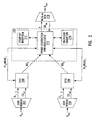
FIGURE 1 is a block diagram of a protocol independent multiplexer according to one aspect of the present invention; -
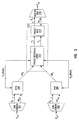
FIGURE 2 is a block diagram of a protocol independent multiplexer according to a first preferred embodiment of the present invention; -
FIGURE 3 is a block diagram of a protocol independent multiplexer according to a second preferred embodiment of the present invention; and -
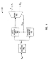
FIGURE 4 is a block diagram of a Clock and Data Recovery (CDR) demultiplexer (DEMUX) device implemented in the multiplexer ofFIGURES 2 and3 according to an exemplary embodiment; -
FIGURE 5 is a block diagram of a frequency agile Phase-Locked-Loop (PLL) implemented in the CDR DEMUX device ofFIGURE 4 according to an exemplary embodiment; -
FIGURE 6 illustrates an exemplary frame structure generated by the frame generation and read logic block implemented withinFIGURE 2 ; -
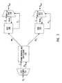
FIGURE 7 is a block diagram of a protocol independent demultiplexer operable with the multiplexer ofFIGURE 2 ; -
FIGURE 8 is a block diagram of a protocol independent demultiplexer operable with the multiplexer ofFIGURE 3 ; and -
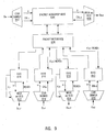
FIGURE 9 is a block diagram of a protocol independent add/drop interface according to an alternative to the second preferred embodiment of the present invention. -
FIGURE 1 illustrates a protocol independent multiplexer according to one aspect of the present invention. This multiplexer comprises first and second inputting devices 102,104, first and second buffering devices 106,108 coupled to the first and second inputting devices 102,104 respectively, and amapping device 110 coupled to the first and second buffering devices 106,108. - Each of the inputting devices 102,104 is operable to receive a respective input signal S1,S2 which is defined by a particular protocol. The input signals are preferably optical input signals but it should be understood that they are not limited to this; for instance, they could be electrical input signals. One skilled in the art would understand that each protocol may have a different bit rate and hence, in previous implementations, require an inputting device designed specifically for that particular bit rate. According to one aspect of the present invention, the inputting devices 102,104 depicted within
FIGURE 1 are capable of being used for a plurality of different protocols that operate at a plurality of different bit rates. In some embodiments this is accomplished with the use of flexible inputting devices that can operate at a number of different fixed bit rates with software flags communicating to the inputting devices which of the fixed bit rates to be utilized in a particular circumstance. In preferred embodiments as are described herein below with reference toFIGURES 2 and3 , the inputting devices do not require software flags as they comprise Clock and Data Recovery (CDR) devices which, as will be described herein below with reference toFIGURES 4 and5 , can determine the bit rate of the respective received signals Sin1,Sin2 and recover data information D1,D2 within the received signals without being given any knowledge of the actual protocol or bit rate that is used. - As depicted within
FIGURE 1 , the first and second buffering devices 106,108 receive the data information D1,D2 output from the first and second inputting devices 102,104 respectively and output respective buffered data information BD1,BD2 to themapping device 110 at outputting periods determined by themapping device 110. Preferably, the percentages of the buffering devices 106,108 that are filled, hereinafter referred to as the fill levels (FL), are communicated to the mapping device. Subsequently, themapping device 110 utilizes the fill levels FL1,FL2 to determine the outputting periods for the buffered data information BD1,BD2 from the buffering devices 106,108 and outputs read signals READ1,READ2 to the buffering devices 106,108. The utilization of the fill levels FL1,FL2 and the subsequent selection of outputting periods can be done in numerous ways, a few of which are described herein below during the description of the preferred embodiments. - Although the fill levels indicating the percentage of the buffering devices that are occupied with data information are utilized in the preferred embodiments, it should be recognized that any fill characteristic could be used. For instance, the fill characteristic could be a ratio between the data information saved within the particular buffering device that has not been output and a maximum amount possible to be saved within the particular buffering device.
- The
mapping device 110, after inputting the buffered data information BD1,BD2 from the buffering devices 106,108 maps this data information into data units consistent with a particular format. The format for a number of preferable data units are described herein below for the preferred embodiments though these are not meant to limit the scope of the present invention. Themapping device 110 then outputs these data units via an output signal Sout which comprises the data information D1,D2 received by both the first and second inputting devices 102,104. Similar to the input signals Sin1, Sin2, the output signal is preferably an optical output signal, but is not limited to this embodiment. - Although the broad aspect of the present invention depicted within
FIGURE 1 only illustrates a multiplexer with two input signals Sin1,Sin2, one skilled in the art would understand that a multiplexer according to the present invention could have more input signals as long as each input signal has a corresponding inputting device and a corresponding buffering device. - Further, although not shown within
FIGURE 1 , a multiplexer according to the present invention could further comprise an outputting device coupled to the output of themapping device 110 to transform the data units of the output signal Sout into a particular format suitable for transmission. - The preferred embodiments of the present invention are now described with reference to
FIGURES 2 through 8 for multiplexer/demultiplexer systems capable of being implemented within optical fiber communication systems.FIGURES 2 and3 illustrate protocol independent multiplexers according to first and second preferred embodiments of the present invention. For these preferred embodiments, the inputting devices, as will be described in detail herein below with reference toFIGURES 4 and5 , are Clock and Data Recovery (CDR) devices combined with demultiplexers (DEMUX), hereinafter referred to as CDR DEMUX devices 202,204. These CDR DEMUX devices 202,204 each receive respective optical input signals Oin1,Oin2, determine the clock rate of the received signal and hence its corresponding bit rate, recover the data information within the received signal, and output the respective clock rate CKin1,CKin2 that is synchronous with the respective optical input signals Oin1,Oin2 along with n signals that together are a demultiplexed version of the data information to the respective buffering device. In these preferable embodiments, the buffering devices are First-In-First-Out (FIFO) memory devices 206,208. -
FIGURE 4 illustrates an exemplary version of the CDR DEMUX device 202 (that is also identical to the CDR DEMUX device 204) that comprises an Optical-to-Electrical (O/E)Converter 402, a frequency agile Phase-Locked-Loop (PLL) 404 coupled to the O/E converter 402, adata recovery unit 406 independently coupled to the O/E converter 402 and the frequencyagile PLL 404, and a demultiplexer (DEMUX) 408 independently coupled to the frequencyagile PLL 404 and thedata recovery unit 406. - The O/
E converter 402 operates to receive the optical signal Oin1 and convert it into an electrical signal Sin1 which is input to both the frequencyagile PLL 404 and thedata recovery unit 406. The frequencyagile PLL 404, as will be described in detail herein below with reference toFIGURE 4 , determines the type of the received signal Sin1 and outputs the clock rate CKin1 that corresponds to the received signal Sin1. Thedata recovery unit 406 utilizes the determined clock rate CKin1 to recover the data information that was transmitted in the optical signal Oin1. The demultiplexer (DEMUX) 408 receives the data information output from thedata recovery unit 406 and outputs n signals that together are a demultiplexed version of the data information. Further, thedemultiplexer 408 forwards the clock rate CKin1 determined at the frequencyagile PLL 404. - The frequency
agile PLL 404 is depicted withinFIGURE 5 and is designed to recover a clock of any frequency on a broad continuous range, from any type of digitally modulated signal. It should be understood that other designs for frequency agile PLLs are possible andFIGURE 5 is provided to show one preferable embodiment. - The circuit comprises a
phase error detector 502, acontrol unit 504, aloop filter 506 coupled to both thephase error detector 502 and thecontrol unit 504, an octave Voltage Controlled Oscillator (VCO) 508 coupled to theloop filter 506, a plurality of clock dividers 510,512,514,516,518,520 coupled in series with theVCO 508, and acontrol selector 522 coupled to theVCO 508 and clock dividers 510-520. Theselector 522 outputs the reference clock CK to be output from thePLL 404. Thephase error detector 502 receives a demodulated digital signal Sin1 comprising the clock to be determined, and the reference clock CK output from theselector 522, detects a phase difference between these two signals and outputs the phase difference, or the phase error signal Ser in a digital format. The signal is input to theloop filter 506 where the high frequency components are removed from the output in accordance with the low-pass characteristics of thisfilter 506. - The circuit preferably uses the
octave VCO 508 in combination with the cascade of clock dividers 510-520.FIGURE 4 shows six dividers-by-two used for the preferred embodiment, but the number of dividers is not limited to 6; more or less of them may be used, according to the frequency range necessary for a certain application. - Since the
VCO 408 can span an octave of frequencies, and the reference clock output by theVCO 508 is divided in frequency by two, four, eight, sixteen, etc., any frequency can be generated at the outputs of the dividers 510-520. Theselector 522 selects a frequency of interest as the recovered clock signal CKin1. The selection can be done in hardware or in software. - The
control unit 504 is used to set the programmable gains for theloop filter 506 and thecontrol selector 522. Thecontrol unit 504 determines the input signal frequency of the signal Sin1 presented at the input of thePLL 404 in order to instruct theselector 522 to choose the value of interest for the recovered clock. The control unit preferably determines the input signal frequency by having a software cycle through the output from the dividers 510-520 from the highest divide ratio (G) to the lowest divide ratio (A) until the PLL lock is obtained. Alternatively, a PLL lock detector could be implemented in hardware at the output of each divider 510-520. In this case, the lowest frequency that a lock is obtained will be the fundamental frequency of the signal Sin1. - An optional Analog-to-Digital Converter (ADC) 524 is shown which may be used to monitor the VCO control voltage to facilitate estimation of the bit-rate of the recovered clock.
- The range of frequencies on which the
PLL 404 may lock is much larger than one octave, thePLL 404 nevertheless requiring only anoctave VCO 508. For example,VCO 508 may operate over the range 2.5 GHz ±33% . The rate for STS-48 (SONET) or STM-16 (SDH) of 2488 MHZ is in this frequency range and would be available at input A ofselector 522. Input B in this case spans the frequency range 2.5GHz 2±33%, which is 1.25GHz±33%. The SONET/SDH STS-24/STM-8 rate of 1244MHz is on this frequency range and would be available at input B ofselector 522. The SONET/SDH STS-12/STM-4 rate would be available at input C, etc. Very importantly, thePLL 404 may also be locked on other, non-SONET/SDH rates in these octave ranges. As examples, both 1062 MHZ (fiber channel) and 1600 MHZ (serial HIPPI) are frequencies on the range available at input B ofselector 522, while 565 MHZ (PDH) is a frequency on the range available at input C, and 44.736 MHZ (DS-3) is a frequency on the range available at input G ofselector 522. - The
PLL 404 bandwidth, K, is determined according to the following equation:
where Kd is the gain of thephase error detector 502, Ko is theVCO 508 gain, Kh is theloop filter 406 gain, dn is the ratio for a divider n (e.g. 1, 2, 4, 8, 16, etc.), n [O,N], N is the number of dividers, and d is the ratio of all dividers, which is 2 in the example ofFIGURE 5 . d was selected 2 in accordance with the use of an octave VCO. - Referring again to
FIGURE 4 , it is recognized that thedemultiplexer 408 is required within the CDR DEMUX devices 202,204 of this preferred embodiment in order to allow the buffering devices (FIFO memory devices 206,208 in this case) and themapping device 110 to be implemented in a technology such as Complementary Metal-Oxide Semiconductor (CMOS) which runs at a slower speed than the clock rate of the received signals Oin1,Oin2. If the buffering devices and mapping devices were implemented within a high-speed process technology that has a processing speed greater than or equal to the received signals Oin1,Oin2, thedemultiplexer 408 may not be required. One possible high-speed process technology is Gallium-Arsenide (GaAs). - Referring again to the preferred embodiments of the protocol independent multiplexer depicted within
FIGURES 2 and3 , the FIFO memory devices 206,208 communicate with themapping device 110 the fill levels FL1, FL2 of the FIFO memory devices 206,208 and themapping device 110 determines the outputting periods for the FIFO memory devices 206,208 with use of read signals READ1,READ2. - In the first preferred embodiment of the present invention depicted within
FIGURE 2 , themapping device 110 maps the buffered data information BD1,BD2 from the FIFO memory devices 206,208 into a frame structure. Themapping device 110, according to this first preferred embodiment, comprises a frame generation and readlogic block 210, a stuffbit insertion block 212, and anoverhead insertion block 214. - The frame generation and read
logic block 210 inputs the fill levels FL1,FL2 from the FIFO memory devices 206,208 and controls the outputting periods of the FIFO memory devices 206,208 with the corresponding read signals READ1,READ2. The key in this first preferred embodiment is that the fill level of the FIFO memory devices 206,208 be maintained substantially in the middle of the available memory with the devices 206,208. There are numerous different implementations for each individual frame though each will include at least one read cycle for each FIFO memory device 206,208, a number of stuff bits that may be grouped as stuff bytes inserted by the stuffbit insertion block 212, and an initial overhead (OH) portion inserted by theoverhead insertion block 214. The OH portion preferably includes information required by a demultiplexer to operate properly such as information relating to the location of the stuff bits and to the bandwidth allocated to each input (the assignments of read cycles within a channel to particular FIFO memory devices 206,208, as is described herein below). Further, the OH portion may include other information such as parity bits. - One exemplary frame structure that could be utilized with the first preferred embodiment is now described with reference to
FIGURE 6 . This particular frame structure comprises an overhead (OH)portion 602 andm frame channels 604 that each comprise N readcycles 606 and one ormore stuff bits 608. The N readcycles 606 within achannel 604 preferably allow for a dynamic bandwidth allocation from the plurality of FIFO memory devices 206,208 by subdividing the transmission bit rate of the entire frame into N portions that are distributed among the FIFO memory devices 206,208. For example, if the frame is to be transmitted at 2.5 GHz and N is set at 16, then each read cycle allocated to a particular FIFO memory device 206,208 would constitute an allocation of 156.25 MHZ. Hence, the minimum bandwidth that can be allocated to a single FIFO memory device 206,208 would be that allocated for one read cycle (156.25 MHZ in the above example) and the maximum would be determined by the speed of the FIFO memory device 206,208 (hence, how many read cycles can be allocated to a particular FIFO memory device within a single channel). Preferably, the bandwidth within each frame for each FIFO memory device 206,208 is allocated based upon the fill levels FL1,FL2 for the particular FIFO memory devices 206,208 with left over bits within the frame being filled with stuff bits. In one embodiment a nominal stuff rate is utilized which directs there to be a set number of stuff bits at predetermined time intervals; this nominal rate being preferably adjustable based on the fill levels FL1,FL2 of the FIFO memory devices 206,208. In one exemplary embodiment, to adjust for differences in fill levels FL1,FL2 during a frame, stuff bits can be added or removed depending upon the need. It is noted that if a large number of stuff bits are grouped together, there is a potential for jitter problems at the demultiplexer due to large time intervals between the arrival of data information. - The number (m) of frame cycles per frame on the other hand is determined by the efficiency that is requested. The efficiency ratio is determined by dividing the number of bits used for the channels by the number of bits used for the entire frame including the overhead (OH)
portion 602. To increase the efficiency, the number of channels per frame can be increased or the number of read cycles per channel can be increased. - Although the first preferred embodiment is described with an exemplary frame structure as illustrated in
FIGURE 6 , this is not meant to limit the scope of the present invention. There are numerous different frame structures that could operate with the first preferred embodiment depicted withinFIGURE 2 so that data information is read from the FIFO memory devices 206,208, a number of stuff bits or bytes is added to the frame, and an overhead (OH) portion is attached to the front of the frame. In fact, the first preferred embodiment would support any frame structure that would allow dynamic allocation of bandwidth to the individual FIFO memory devices 206,208 so that the fill levels of the FIFO memory devices 206,208 are maintained substantially at a predetermined desired level or range such as 50 % full. - Now referring to
FIGURE 3 , themapping device 110 according to the second preferred embodiment comprises a packetinterface logic block 310 and a packet multiplexer (MUX) 312. In this second preferred embodiment, the packetinterface logic block 310 is input with the fill levels FL1,FL2 of the FIFO memory devices 206,208 so that theblock 310 can determine when there is sufficient data information to create a packet. Preferably, once it is determined that sufficient data information is buffered within one of the FIFO memory devices 206,208, the packetinterface logic block 310 activates a read cycle with the corresponding read signal READ1,READ2 which triggers the outputting of the buffered data information BD1,BD2 within the particular FIFO memory device 206,208. Preferably, the read rate is higher than the write rate and so the corresponding FIFO memory device 206,208 empties during the read cycle. The read cycle, according to the second preferred embodiment, is terminated once a predetermined low level of data information is buffered within the particular FIFO memory device 206,208. The packetinterface logic block 310 further formats the data information into a standard packet format, preferably including a header and trailer, and forwards these packets P1,P2 corresponding to respective FIFO memory devices 206,208 to thepacket MUX 312. - It is noted that, as depicted within
FIGURE 3 , one packetinterface logic block 310 is servicing a plurality of FIFO memory devices 206,208. This can only occur if the read rate is sufficiently high; otherwise, each FIFO memory device 206,208 should have a corresponding packetinterface logic block 310. - The
packet MUX 312 inserts the packets received from the packet interface logic block(s) 310 into a frame structure that can be used for transmitting. The unused bandwidth can be filled with idle packets. Thepacket MUX 312 further can be utilized to assign output ports and perform connection management and ADM functions. Although preferably thepacket MUX 312 is a custom designed part, it is noted that an industry standard part may be utilized. - The next component in both the first and second preferred embodiments, as depicted within
FIGURES 2 and3 , is a multiplexer (MUX) with VCO block 216 that corresponds to the outputting device mentioned above with reference toFIGURE 1 . This is preferably a well known component that receives portions of the frames in parallel at a first slow bit rate and multiplexes them at a clock rate (CKout) that is sufficient to output the frames on an optical signal Oout at a bit rate consistent with the optical fiber utilized. Preferably, this MUX withVCO block 216 is formatted to operate with SONET and so the output bit rate should be 2.5 GHz. - One key difference between the implementations of the first and second preferred embodiments is the read signals READ1,READ2. In the first preferred embodiment, the read signals READ1,READ2 are synchronous with the optical output signal Oout of the multiplexer with gaps inserted for the OH portion and the stuff bits. On the other hand, the read signals READ1,READ2 within the second preferred embodiment of
FIGURE 3 are preferably asynchronous. - Demultiplexers that preferably operate with the multiplexers of the first and second preferred embodiments are now described with reference to
FIGURES 7 and8 respectively. The demultiplexer ofFIGURE 7 that operates with the multiplexer of the first preferred embodiment comprises aCDR DEMUX device 702, a frame removal and writelogic block 704 coupled to theCDR DEMUX device 702, first and second FIFO memory devices 706,708 coupled independently to the frame removal and writelogic block 704, and first and second MUX with VCO blocks 710,712 coupled independently to the FIFO memory devices 706,708. - The
CDR DEMUX device 702 preferably operates to receive an optical signal Oin from an optical fiber, demultiplex the received optical signal Oin, and output n signals that together comprises the received optical signal Oin. - The frame removal and write
logic block 704 receives the demultiplexed signals from theCDR DEMUX device 702, recovers the frames from the demultiplexed signals n, and utilizes the overhead (OH) portions to determine the location of the stuff bits and to determine which read cycles were assigned to which FIFO memory device 206,208 (input signal Oin1,Oin2). After reading the overhead portion, the frame removal and writelogic block 704 removes the overhead portion and the stuff bits and writes the data information contained within the channels to the appropriate FIFO memory device 706,708. - Preferably, the MUX with VCO blocks 710,712, at the same time, read data information out of the corresponding FIFO memory devices 706,708 and output the data via respective optical signals Oout1,Oout2 to optical fibers. Fill levels FL1,FL2 output from the FIFO memory devices 706,708 are preferably used by the VCOs within the blocks 710,712 to adjust the frequency of the VCOs in order to maintain the fill levels FL1, FL2 substantially at a predetermined desired level or range such as 50% full.
- The demultiplexer of
FIGURE 8 that operates with the multiplexer of the second preferred embodiment is similar to that ofFIGURE 7 , but replaces the frame removal and writelogic block 704 with a packet demultiplexer (DEMUX) 804 coupled in series with a packetinterface logic block 806. Thepacket DEMUX 804 recovers the packets that are sent via the incoming data stream output from theCDR DEMUX device 702 and forwards these packets to their assigned packet interface port within the packetinterface logic block 806. The packetinterface logic block 806 removes the data encapsulation (if any was required by the packet MUX 312) and writes the data information contained within the packets to the appropriate FIFO memory device 706,708. The remaining components of the demultiplexer depicted withinFIGURE 8 operate similarly to the components described previously for the demultiplexer ofFIGURE 7 . - One key consideration that must be made concerning the demultiplexers of
FIGURES 7 and8 is the problem of output jitter on the output optical signals Oout1, Oout2. To reduce jitter, the bandwidth of the PLL must be sufficiently low to filter out variations in data arrival times. To reduce the probability of jitter problems many well-known techniques can be utilized such as increasing the amount of memory within the FIFO memory devices 706,708 to reduce periods in which the FIFO memory devices 706,708 are potentially empty. - An alternative embodiment of the present invention is now described with reference to
FIGURE 9 for an add/drop interface that combines the multiplexer and demultiplexer of the second preferred embodiment. This interface comprises a CDR DEMUX device 902 that is preferably the same as theCDR DEMUX device 702 coupled in series with a packet add/drop multiplexer (MUX) block 904 and a MUX with VCO block 906 that is preferably the same as the MUX withVCO block 216. Further, coupled to the packet add/drop MUX block 904 is apacket interface block 908 which has a plurality of inputting FIFO memory devices 910,912 and a plurality of outputting FIFO memory devices 914,916 attached. Each of the inputting FIFO memory devices 910,912 are further coupled to a respective CDR DEMUX device 918,920 and each of the outputtingFIFO memory devices - The CDR DEMUX device 902 receives an optical input signal Oin, determines the input clock rate CKin of the optical input signal Oin, and outputs the clock rate CKin and demultiplexed signals that together comprise the optical input signal Oin. The packet add/
drop MUX block 904 receives demultiplexed signals and the input clock rate CKin and determines, with use of packet headers, which packets should be forwarded onward through the MUX withVCO block 906 and which packets should be forwarded to thepacket interface block 908 for processing at the interface. Further, the packet add/drop MUX block 904 receives other packets from thepacket interface block 908 that are then also forwarded to the MUX withVCO block 906. The MUX withVCO block 906 operates as described for the MUX withVCO block 216, outputting an optical output signal Oout. - The
packet interface block 908 operates similar to the combination of the packetinterface logic block 310 and the packetinterface logic block 806. The CDR DEMUX devices 918,920 along with the inputting FIFO memory devices 910,912 operate the same as the similar components inFIGURES 2 and3 . The outputting FIFO memory devices 914,916 combined with the MUX with VCO blocks 922,924 operate the same as the similar components inFIGURES 7 and8 . Hence, the add function of this add/drop interface operates with optical input signals Oin1,Oin2 received at the CDR DEMUX devices 918,920 being forwarded through the inputting FIFO memory devices 910,912, converted into packets within thepacket interface block 908, and forwarded through the packet add/drop MUX 904 and the MUX with VCO block 906 to the optical output signal Oout. Similarly, the drop function operates as packets are forwarded to thepacket interface block 908 from the packet add/drop MUX block 904. The packets are then reformatted and forwarded via the outputting FIFO memory devices 914,916 to the respective MUX with VCO blocks 922,924 where data information within the dropped packets can be output in corresponding optical output signals Out1,Out2. - There are numerous advantages to both the first and second preferred embodiments of the present invention. The second preferred embodiment can leverage industry investment in packet MUX technology, such as implemented within
packet MUX block 312, to provide additional functionality. Further, the packet based solution provides simplification over the first preferred embodiment since there is no need to provision the bandwidth of any given input port, as thepacket MUX block 312 automatically accommodates for variations in the input rate. Yet further, the granularity of the bandwidth allocation is improved for the packet based solution compared to the frame generation and bit stuffing solution. In the packet based solution, the bandwidth allocation for each input port is only limited by the defined packet size while the frame generation and bit stuffing solution is limited by the divide ratio of the number of read cycles by the rate the frame is to be transmitted at. In addition, the packet based solution of the second preferred embodiment has the possibility of added value by enabling add/drop functionality as described in the alternative embodiment ofFIGURE 9 , by combining the protocol independent multiplexing of the present invention with switched Ethernet interfaces on the same wavelength, and/or by allowing compatibility with existing packet based networks for transmission over existing Internet Protocol (IP) or Asynchronous Transfer Mode (ATM) infrastructures. - On the other hand, the frame generation and bit stuffing solution of the first preferred embodiment is simpler if a packet MUX block is not already available. Further, the packet based solution has a larger potential of having jitter problems at the demultiplexer due to the time interval between transmissions of data information. Yet further, the overhead portion utilized in the first preferred embodiment can provide additional benefits such as internode communication channels, the ability to monitor and/or correct bit errors, signalling for protection signalling and fault isolation, and end to end connection verification. If the frame format defined is compatible with preexisting standards, the frame generation and bit stuffing solution could allow for the multiplexed signal to be carried over existing networks such as SONET networks.
- In either case, the key advantages to the present invention are the ability of the present invention to multiplex signals without the knowledge of the protocols to be utilized being known at the time of implementation and the ability of the multiplexer to dynamically allocate bandwidth to the various input signals. The first key advantage allows a single piece of hardware to be used with a multitude of different protocols, therefore not requiring large inventories of numerous different multiplexers and demultiplexers that are specific to a limited number of protocols. As well, the use of the present invention could reduce the number of service visits that would be required to replace hardware when new protocols are introduced and could increase the time to market of new services as no hardware changes would be required to carry the new service over the network.
- The ability to dynamically allocate bandwidth to the various input signals allows better utilization of the bandwidth within a channel with unknown bit rates, hereinafter referred to as a transparent channel. This improved efficiency reduces the cost of implementing transparent services that utilize transparent channels. Further, the dynamic bandwidth allocation allows for increased flexibility for the combining of a single high bandwidth service with a plurality of low bandwidth services which have a minimal incremental cost.
- Although the preferred embodiments have been described in detail herein above, this is not meant to limit the scope of the present invention. For instance, the "trib" functions, such as the CDR DEMUX devices 202,204 and FIFO memory devices 206,208 within the multiplexers and the FIFO memory devices 706,708 and MUX with VCO blocks 710,712 within the demultiplexers, could be implemented on separate cards from the remaining components. This enables separate protection of these "trib" components and allow for sub-equipping of "trib" components for lower initial costs.
- Another limitation of the preferred embodiments that is not meant to limit the scope of the present invention is the described use of either frames in the first preferred embodiment and packets in the second preferred embodiment. In fact, the mapping device can map the data information input from the buffering devices into any data unit that is defined for, as long as the receiving of data information is done based upon the fill characteristic.
- Although the multiplexers of the preferred embodiments have been illustrated in
FIGURES 2 and3 as having only two input optical signals Oin1,Oin2, one skilled in the art would understand that the multiplexers could be implemented with more optical signals as long as each optical signal had acorresponding inputting device 104 andbuffering device 106. Similar, expansions onFIGURES 7 ,8 , and9 could be contemplated. - Further, although the preferred embodiments of the present invention are directed to multiplexers and demultiplexers, it can be seen that the multiplexer of
FIGURES 2 or3 can be reduced to a single input optical signal. In this case, only asingle inputting device 102 and asingle buffering device 106 would be required. Hence, rather than operating as a multiplexer, the modified device would operate as an interface device between two protocols, the bit rate of the input optical signal either being detected by a CDR DEMUX device or being indicated through a software flag. In this implementation, the interface device would comprise an inputting device, a buffering device, a mapping device, and preferably an outputting device. - Persons skilled in the art will appreciate that there are yet more alternative implementations and modifications possible to provide a protocol independent multiplexer and/or demultiplexer, and that the above implementations are only illustrations of these embodiments of the invention. The scope of the invention, therefore, is only to be limited by the claims appended hereto.
Claims (18)
- A multiplexer comprising:means (202, 204) for receiving at least two data signals each having any of a plurality of nominal bit rates and any of a plurality of protocols;means (202, 204) for recovering data information within each of the received data signals;means (206, 208) for buffering the recovered data information from each of the received data signals such that the recovered data information corresponding to each of the received data signals is output at determined outputting periods;means (110) for monitoring fill characteristics within the means (206, 208) for buffering;means (110) for determining the outputting periods for the means (206, 208) for buffering with use of the fill characteristics; andmeans (110) for mapping the recovered data information corresponding to each of the received data signals output from the means (206, 208) for buffering into data units and outputting the data units,wherein the means (202, 204) for recovering is arranged to recover data information within each of the received data signals having any of a plurality of nominal bit rates and any of a plurality of protocols by:determining the bit rate either by receiving a software flag indicative of the bit rate or by recovering a clock rate of the data signal; andrecovering the data information within the received data signal with use of the determined bit rate.
- A multiplexer according to claim 1, in which the means (202, 204) for receiving at least two data signals and for recovering data information comprises at least two inputting devices (102, 104), each adapted to receive a data signal at a particular bit rate, recover data information within the received data signal with use of the particular bit rate, and output the data information;
the means (206, 208) for buffering comprises buffering devices (106, 108) connected respectively to the inputting devices (102, 104), each buffering device (106, 108) being adapted to receive the recovered data information from its respective inputting device (102, 104), save the data information, and output the recovered data information at determined outputting periods; and
the means (110) for monitoring, determining and mapping comprises a mapping device (110) connected to the buffering devices (106, 108) and adapted to monitor a fill characteristic within each of the buffering devices (106, 108), determine the outputting periods for each of the buffering devices (106, 108) with use of the corresponding fill characteristic, receive the data information output from each of the buffering devices (106, 108), map the received data information into data units, and output the data units. - A multiplexer according to claim 2, further comprising an outputting device (216), coupled to the mapping device (110), that is adapted to receive the data units and transform the data units into a particular format suitable for transmission the format having any of a plurality of nominal bit rates and any of a plurality of protocols.
- A multiplexer according to claim 3, wherein the data signals received at the inputting devices (102, 104) are optical signals and each of the inputting devices (102, 104) comprises an Optical-to-Electrical converter (402); and
wherein the outputting device (216) comprises an Electrical-to-Optical converter and the particular format suitable for transmission is an optical format. - A multiplexer according to claim 3, wherein each of the inputting devices (102, 104) is further adapted to demultiplex the data information into a plurality of data information segments, the outputting of the data information from the inputting devices (102, 104) being in the form of the data information segments; and
wherein the outputting device (216) is adapted to multiplex a plurality of the data units into a signal suitable for transmission. - A multiplexer according to any of claims 2 to 5, wherein the buffering devices (106, 108) and the mapping device (110) are produced with a Complementary Metal Oxide Semiconductor (CMOS) process.
- A multiplexer according to any of claims 2 to 6, wherein each of the buffering devices (106, 108) is a First-In-First-Out memory device (206, 208).
- A multiplexer according to any of claims 2 to 7, wherein the fill characteristic is a ratio between the data information saved within the buffering device (106, 108) that has not been output and a maximum amount possible to be saved within the particular buffering device (106, 108).
- A multiplexer according to claim 8, wherein the mapping device (110) is adapted to determine the outputting periods for each of the buffering devices (106, 108) in order to maintain the fill characteristics near 50%.
- A multiplexer according to any of claims 2 to 9, wherein the mapping device (110) is a frame generation device and the mapping of the received data information into data units comprises the step of generating a plurality of frames;
wherein each of the frames comprise an overhead portion and a plurality of data sections, each of the data sections comprising the data information received from one of the buffering devices (206, 208) during one of the outputting periods; and
wherein the overhead portion comprises information required to remove the frame structure from the data information. - A multiplexer according to claim 10, wherein the mapping device (110) is adapted to determine the outputting periods for each of the buffering devices (206, 208) by allocating each of the buffering devices (206, 208) a set number of the outputting periods in each of the frames.
- A multiplexer according to claim 11, wherein the set number is determined dynamically for each frame based upon the fill characteristics of the buffering devices (206, 208).
- A multiplexer according to claim 11 or 12, wherein each of the frames further comprises at least one stuff bit that fills up unused space within the particular frame and the overhead portion further comprises information required to remove the stuff bits.
- A multiplexer according to claim 13, wherein the stuff bits are dynamically allocated within each of the frames based upon the fill characteristics of the buffering devices.
- A multiplexer according to any of claims 2 to 9, wherein the mapping device (110) is a packet generation device and the mapping of the received data information into data units comprises the step of generating a plurality of packets;
wherein each of the packets comprise a header portion and at least one data section, the data section comprising the data information received from one of the buffering devices (206, 208) during one of the outputting periods. - A multiplexer according to claim 15, wherein the fill characteristics are measures of the amount of saved data information within each of the buffering devices (206, 208); and
wherein the mapping device (110) is adapted to determine the outputting periods for one of the buffering devices by determining when the respective amount of saved data information within the buffering device (206, 208) is sufficient to fill the data section of one of the packets. - A multiplexer according to claim 16, wherein each of the packets is an Internet Protocol packet.
- A multiplexer according to claim 16, wherein each of the packets is an Asynchronous Transfer Mode cell.
Applications Claiming Priority (2)
| Application Number | Priority Date | Filing Date | Title |
|---|---|---|---|
| US09/307,812 US6522671B1 (en) | 1999-05-10 | 1999-05-10 | Protocol independent sub-rate device |
| US307812 | 2002-12-02 |
Publications (3)
| Publication Number | Publication Date |
|---|---|
| EP1052794A2 EP1052794A2 (en) | 2000-11-15 |
| EP1052794A3 EP1052794A3 (en) | 2002-05-22 |
| EP1052794B1 true EP1052794B1 (en) | 2012-08-29 |
Family
ID=23191261
Family Applications (1)
| Application Number | Title | Priority Date | Filing Date |
|---|---|---|---|
| EP00303925A Expired - Lifetime EP1052794B1 (en) | 1999-05-10 | 2000-05-10 | Protocol independent sub-rate device |
Country Status (4)
| Country | Link |
|---|---|
| US (2) | US6522671B1 (en) |
| EP (1) | EP1052794B1 (en) |
| JP (1) | JP4416268B2 (en) |
| CA (1) | CA2304118C (en) |
Families Citing this family (30)
| Publication number | Priority date | Publication date | Assignee | Title |
|---|---|---|---|---|
| US6522671B1 (en) * | 1999-05-10 | 2003-02-18 | Nortel Networks Limited | Protocol independent sub-rate device |
| JP2000324110A (en) * | 1999-05-10 | 2000-11-24 | Mitsubishi Electric Corp | Communication method and communication device |
| US20020039211A1 (en) * | 1999-09-24 | 2002-04-04 | Tian Shen | Variable rate high-speed input and output in optical communication networks |
| US6937614B1 (en) | 1999-11-12 | 2005-08-30 | Nortel Networks Limited | Transparent port for high rate networking |
| KR100363884B1 (en) * | 1999-12-27 | 2002-12-11 | 한국전자통신연구원 | Internet Protocol Over WDM Network, and Packet Communication System and Method in the IPOW Network |
| JP3478228B2 (en) * | 2000-03-07 | 2003-12-15 | 日本電気株式会社 | Speed conversion circuit and control method thereof |
| US7228077B2 (en) * | 2000-05-12 | 2007-06-05 | Forster Energy Llc | Channel gain control for an optical communications system utilizing frequency division multiplexing |
| US7260099B1 (en) * | 2000-07-14 | 2007-08-21 | Nortel Networks Limited | Processing of arbitrarily formatted client signals to achieve compatibility with existing transport networks |
| US6822975B1 (en) * | 2000-09-08 | 2004-11-23 | Lucent Technologies | Circuitry for mixed-rate optical communication networks |
| US7263550B1 (en) * | 2000-10-10 | 2007-08-28 | Juniper Networks, Inc. | Agent-based event-driven web server architecture |
| US20020105696A1 (en) * | 2001-02-07 | 2002-08-08 | Ross Halgren | Transparent optical-electronic-optical switch |
| US20020135835A1 (en) * | 2001-03-06 | 2002-09-26 | Richard Lauder | Optical traffic grooming |
| US20020186430A1 (en) * | 2001-06-12 | 2002-12-12 | Ross Halgren | Communications network |
| US7161961B2 (en) * | 2001-06-13 | 2007-01-09 | International Business Machines Corporation | STM-1 to STM-64 SDH/SONET framer with data multiplexing from a series of configurable I/O ports |
| WO2003017123A1 (en) * | 2001-08-16 | 2003-02-27 | Redline Networks, Inc. | System and method for maintaining statefulness during client-server interactions |
| US7075951B1 (en) * | 2001-11-29 | 2006-07-11 | Redback Networks Inc. | Method and apparatus for the operation of a storage unit in a network element |
| US20030161351A1 (en) * | 2002-02-22 | 2003-08-28 | Beverly Harlan T. | Synchronizing and converting the size of data frames |
| US7286471B2 (en) * | 2002-03-23 | 2007-10-23 | Mindspeed Technologies, Inc. | Dynamic bandwidth allocation for wide area networks |
| US7161965B2 (en) * | 2002-03-29 | 2007-01-09 | Bay Microsystems, Inc. | Add/drop multiplexor with aggregate serializer/deserializers |
| US7145922B2 (en) * | 2002-03-29 | 2006-12-05 | Bay Microsystems, Inc. | Composite add/drop multiplexor with crisscross loop back |
| US7324548B2 (en) * | 2002-11-01 | 2008-01-29 | Broadcom Corporation | Transceiver system and method supporting variable rates and multiple protocols |
| JP4439514B2 (en) * | 2004-04-23 | 2010-03-24 | パナソニック株式会社 | Receiving device, receiving system using the receiving device, and receiving method thereof |
| US7664139B2 (en) * | 2005-09-16 | 2010-02-16 | Cisco Technology, Inc. | Method and apparatus for using stuffing bytes over a G.709 signal to carry multiple streams |
| JP2007096822A (en) * | 2005-09-29 | 2007-04-12 | Fujitsu Ltd | Signal multiplxer and its stuff control method |
| EP1858276B8 (en) | 2006-05-15 | 2018-05-02 | Nokia Solutions and Networks GmbH & Co. KG | Interface for efficiently transmitting digital signals |
| US7870363B2 (en) * | 2007-12-28 | 2011-01-11 | Intel Corporation | Methods and arrangements to remap non-volatile storage |
| EP2247008A4 (en) * | 2008-02-08 | 2017-05-17 | NEC Corporation | Radio transmitting device and radio transmitting method |
| US8595538B2 (en) * | 2008-03-03 | 2013-11-26 | Quintic Holdings | Single-clock-based multiple-clock frequency generator |
| US20150032917A1 (en) * | 2012-02-22 | 2015-01-29 | Vincent Nguyen | Multiplexer for signals according to different protocols |
| JP5993776B2 (en) * | 2013-03-29 | 2016-09-14 | 株式会社日立製作所 | Data transmission system and receiving apparatus |
Family Cites Families (34)
| Publication number | Priority date | Publication date | Assignee | Title |
|---|---|---|---|---|
| US4965787A (en) * | 1989-02-09 | 1990-10-23 | Data General Corporation | Methods and apparatus for multiplexing sub-rate channels in a digital data communication system |
| FR2681205B1 (en) * | 1991-09-09 | 1994-05-06 | Hewlett Packard Co | MULTIPLEXING METHOD AND DEVICE. |
| JPH06169320A (en) * | 1992-10-02 | 1994-06-14 | Toshiba Corp | Atm cell making device |
| JPH06197120A (en) * | 1992-12-24 | 1994-07-15 | Nippon Telegr & Teleph Corp <Ntt> | Cell multiplex circuit |
| US5396492A (en) * | 1993-04-28 | 1995-03-07 | At&T Corp. | Method and apparatus for adaptive clock recovery |
| US5414707A (en) * | 1993-12-01 | 1995-05-09 | Bell Communications Research, Inc. | Broadband ISDN processing method and system |
| JPH07297830A (en) * | 1994-04-21 | 1995-11-10 | Mitsubishi Electric Corp | Multiplexer, non-multiplexer, switching device, and network adapter |
| JP3458469B2 (en) * | 1994-07-15 | 2003-10-20 | ソニー株式会社 | Signal receiving apparatus and communication method |
| DE4442654C1 (en) * | 1994-11-30 | 1996-05-23 | Siemens Ag | Method for reducing runtime fluctuations in ATM cells |
| JP3264803B2 (en) | 1995-09-25 | 2002-03-11 | 富士通株式会社 | Add / drop multiplexer supporting fixed length cells |
| US5867543A (en) * | 1996-03-29 | 1999-02-02 | Dsc Communications Corporation | Multi-rate transmission system |
| US5914962A (en) * | 1996-06-27 | 1999-06-22 | Zenith Electronics Corporation | MPEG transport mux for independently clocked transport streams |
| US6122281A (en) | 1996-07-22 | 2000-09-19 | Cabletron Systems, Inc. | Method and apparatus for transmitting LAN data over a synchronous wide area network |
| KR100323159B1 (en) * | 1996-12-11 | 2002-03-08 | 포만 제프리 엘 | Digital cross connect and add/drop multiplexing device for sdh or sonet signals |
| JPH10173674A (en) * | 1996-12-13 | 1998-06-26 | Hitachi Ltd | Digital data transmission system |
| US6047002A (en) * | 1997-01-16 | 2000-04-04 | Advanced Micro Devices, Inc. | Communication traffic circle system and method for performing packet conversion and routing between different packet formats including an instruction field |
| US6058109A (en) * | 1997-02-04 | 2000-05-02 | The Kohl Group, Inc. | Combined uniform rate and burst rate transmission system |
| DE19704299C2 (en) | 1997-02-06 | 1999-04-01 | Deutsche Telekom Ag | Device for obtaining a clock signal from a data signal and bit rate detection device for determining a bit rate |
| US6452933B1 (en) * | 1997-02-07 | 2002-09-17 | Lucent Technologies Inc. | Fair queuing system with adaptive bandwidth redistribution |
| US5841760A (en) | 1997-04-24 | 1998-11-24 | Northern Telecom Limited | Transparent multiplexer/demultiplexer |
| EP0876016B1 (en) * | 1997-05-02 | 2006-03-22 | Lsi Logic Corporation | Adaptive digital clock recovery |
| US6047000A (en) * | 1997-07-24 | 2000-04-04 | The Hong Kong University Of Science & Technology | Packet scheduling system |
| JP3109465B2 (en) * | 1997-12-04 | 2000-11-13 | 日本電気株式会社 | Digital PLL circuit and signal reproducing method |
| US6307836B1 (en) * | 1997-12-10 | 2001-10-23 | Mci Communications Corporation | High-speed transparent access to multiple services |
| US6785289B1 (en) * | 1998-06-05 | 2004-08-31 | Sarnoff Corporation | Method and apparatus for aligning sub-stream splice points in an information stream |
| US6356546B1 (en) * | 1998-08-11 | 2002-03-12 | Nortel Networks Limited | Universal transfer method and network with distributed switch |
| US6580721B1 (en) * | 1998-08-11 | 2003-06-17 | Nortel Networks Limited | Routing and rate control in a universal transfer mode network |
| US6628652B1 (en) * | 1998-09-18 | 2003-09-30 | Lucent Technologies Inc. | Flexible telecommunications switching network |
| US6522671B1 (en) * | 1999-05-10 | 2003-02-18 | Nortel Networks Limited | Protocol independent sub-rate device |
| US7002986B1 (en) * | 1999-07-08 | 2006-02-21 | Nortel Networks Limited | Mapping arbitrary signals into SONET |
| US6430715B1 (en) * | 1999-09-17 | 2002-08-06 | Digital Lightwave, Inc. | Protocol and bit rate independent test system |
| US6636529B1 (en) * | 1999-10-07 | 2003-10-21 | Nortel Networks Limited | Semi transparent tributary for synchronous transmission |
| US7075951B1 (en) * | 2001-11-29 | 2006-07-11 | Redback Networks Inc. | Method and apparatus for the operation of a storage unit in a network element |
| US7061867B2 (en) * | 2002-04-02 | 2006-06-13 | Intel Corporation | Rate-based scheduling for packet applications |
-
1999
- 1999-05-10 US US09/307,812 patent/US6522671B1/en not_active Expired - Lifetime
-
2000
- 2000-04-05 CA CA2304118A patent/CA2304118C/en not_active Expired - Lifetime
- 2000-04-19 JP JP2000117870A patent/JP4416268B2/en not_active Expired - Lifetime
- 2000-05-10 EP EP00303925A patent/EP1052794B1/en not_active Expired - Lifetime
-
2003
- 2003-01-24 US US10/349,939 patent/US7590153B2/en not_active Expired - Lifetime
Also Published As
| Publication number | Publication date |
|---|---|
| EP1052794A3 (en) | 2002-05-22 |
| JP4416268B2 (en) | 2010-02-17 |
| JP2000332717A (en) | 2000-11-30 |
| US20030133475A1 (en) | 2003-07-17 |
| CA2304118A1 (en) | 2000-11-10 |
| EP1052794A2 (en) | 2000-11-15 |
| CA2304118C (en) | 2011-03-22 |
| US6522671B1 (en) | 2003-02-18 |
| US7590153B2 (en) | 2009-09-15 |
Similar Documents
| Publication | Publication Date | Title |
|---|---|---|
| EP1052794B1 (en) | Protocol independent sub-rate device | |
| US7002986B1 (en) | Mapping arbitrary signals into SONET | |
| US5850387A (en) | Processor device for terminating and creating synchronous transport signals | |
| EP1518366B1 (en) | Transparent flexible concatenation | |
| US7957429B2 (en) | Transmission system | |
| US7130276B2 (en) | Hybrid time division multiplexing and data transport | |
| EP1085686B1 (en) | Transport system and transport method | |
| US6765933B1 (en) | Inter-chip port and method for supporting high rate data streams in SDH and SONET transport networks | |
| US7085293B2 (en) | Scaleable transport of TDM channels in a synchronous frame | |
| JPH10209995A (en) | Transmitting device | |
| US5490142A (en) | VT group optical extension interface and VT group optical extension format method | |
| WO2003032540A2 (en) | Method and apparatus for digital data synchronization | |
| EP1705817B1 (en) | Apparatus for transmitting data using virtual concatenation | |
| EP1537694B1 (en) | Synchronous transmission network node | |
| WO2023278022A1 (en) | System and method for performing rate adaptation of constant bit rate (cbr) client data with a fixed number of idle blocks for transmission over a metro transport network (mtn) | |
| US6915348B1 (en) | Validation of a connection between arbitrary end-points in a communications network using an augmented SPE | |
| US11838111B2 (en) | System and method for performing rate adaptation of constant bit rate (CBR) client data with a variable number of idle blocks for transmission over a metro transport network (MTN) | |
| US7570660B1 (en) | Apparatus for implementing transparent subwavelength networks | |
| US7715443B1 (en) | Boundary processing between a synchronous network and a plesiochronous network | |
| Manke et al. | Dynamic Buffer Allocation–A New Approach to Reduce Buffer Size at Receiver in VCAT Enabled Next Generation SDH Networks |
Legal Events
| Date | Code | Title | Description |
|---|---|---|---|
| PUAI | Public reference made under article 153(3) epc to a published international application that has entered the european phase |
Free format text: ORIGINAL CODE: 0009012 |
|
| AK | Designated contracting states |
Kind code of ref document: A2 Designated state(s): AT BE CH CY DE DK ES FI FR GB GR IE IT LI LU MC NL PT SE |
|
| AX | Request for extension of the european patent |
Free format text: AL;LT;LV;MK;RO;SI |
|
| PUAL | Search report despatched |
Free format text: ORIGINAL CODE: 0009013 |
|
| AX | Request for extension of the european patent |
Free format text: AL;LT;LV;MK;RO;SI |
|
| 17P | Request for examination filed |
Effective date: 20021023 |
|
| AKX | Designation fees paid |
Designated state(s): DE FR GB |
|
| RAP1 | Party data changed (applicant data changed or rights of an application transferred) |
Owner name: NORTEL NETWORKS LIMITED |
|
| 17Q | First examination report despatched |
Effective date: 20031229 |
|
| RAP1 | Party data changed (applicant data changed or rights of an application transferred) |
Owner name: CIENA LUXEMBOURG S.A.R.L. |
|
| GRAP | Despatch of communication of intention to grant a patent |
Free format text: ORIGINAL CODE: EPIDOSNIGR1 |
|
| GRAS | Grant fee paid |
Free format text: ORIGINAL CODE: EPIDOSNIGR3 |
|
| GRAA | (expected) grant |
Free format text: ORIGINAL CODE: 0009210 |
|
| AK | Designated contracting states |
Kind code of ref document: B1 Designated state(s): DE FR GB |
|
| REG | Reference to a national code |
Ref country code: GB Ref legal event code: FG4D |
|
| REG | Reference to a national code |
Ref country code: DE Ref legal event code: R096 Ref document number: 60047459 Country of ref document: DE Effective date: 20121025 |
|
| PLBE | No opposition filed within time limit |
Free format text: ORIGINAL CODE: 0009261 |
|
| STAA | Information on the status of an ep patent application or granted ep patent |
Free format text: STATUS: NO OPPOSITION FILED WITHIN TIME LIMIT |
|
| 26N | No opposition filed |
Effective date: 20130530 |
|
| REG | Reference to a national code |
Ref country code: DE Ref legal event code: R097 Ref document number: 60047459 Country of ref document: DE Effective date: 20130530 |
|
| REG | Reference to a national code |
Ref country code: FR Ref legal event code: PLFP Year of fee payment: 17 |
|
| REG | Reference to a national code |
Ref country code: FR Ref legal event code: PLFP Year of fee payment: 18 |
|
| REG | Reference to a national code |
Ref country code: FR Ref legal event code: PLFP Year of fee payment: 19 |
|
| PGFP | Annual fee paid to national office [announced via postgrant information from national office to epo] |
Ref country code: DE Payment date: 20190521 Year of fee payment: 20 |
|
| PGFP | Annual fee paid to national office [announced via postgrant information from national office to epo] |
Ref country code: FR Payment date: 20190522 Year of fee payment: 20 |
|
| PGFP | Annual fee paid to national office [announced via postgrant information from national office to epo] |
Ref country code: GB Payment date: 20190521 Year of fee payment: 20 |
|
| REG | Reference to a national code |
Ref country code: DE Ref legal event code: R071 Ref document number: 60047459 Country of ref document: DE |
|
| REG | Reference to a national code |
Ref country code: GB Ref legal event code: PE20 Expiry date: 20200509 |
|
| PG25 | Lapsed in a contracting state [announced via postgrant information from national office to epo] |
Ref country code: GB Free format text: LAPSE BECAUSE OF EXPIRATION OF PROTECTION Effective date: 20200509 |