EP1016939B1 - Image developing apparatus, process cartridge, electrophotographic image forming apparatus, and development unit frame - Google Patents
Image developing apparatus, process cartridge, electrophotographic image forming apparatus, and development unit frame Download PDFInfo
- Publication number
- EP1016939B1 EP1016939B1 EP99310455A EP99310455A EP1016939B1 EP 1016939 B1 EP1016939 B1 EP 1016939B1 EP 99310455 A EP99310455 A EP 99310455A EP 99310455 A EP99310455 A EP 99310455A EP 1016939 B1 EP1016939 B1 EP 1016939B1
- Authority
- EP
- European Patent Office
- Prior art keywords
- developer
- electroconductive portion
- carrier member
- forming apparatus
- process cartridge
- Prior art date
- Legal status (The legal status is an assumption and is not a legal conclusion. Google has not performed a legal analysis and makes no representation as to the accuracy of the status listed.)
- Expired - Lifetime
Links
Images


Classifications
-
- G—PHYSICS
- G03—PHOTOGRAPHY; CINEMATOGRAPHY; ANALOGOUS TECHNIQUES USING WAVES OTHER THAN OPTICAL WAVES; ELECTROGRAPHY; HOLOGRAPHY
- G03G—ELECTROGRAPHY; ELECTROPHOTOGRAPHY; MAGNETOGRAPHY
- G03G15/00—Apparatus for electrographic processes using a charge pattern
-
- G—PHYSICS
- G03—PHOTOGRAPHY; CINEMATOGRAPHY; ANALOGOUS TECHNIQUES USING WAVES OTHER THAN OPTICAL WAVES; ELECTROGRAPHY; HOLOGRAPHY
- G03G—ELECTROGRAPHY; ELECTROPHOTOGRAPHY; MAGNETOGRAPHY
- G03G21/00—Arrangements not provided for by groups G03G13/00 - G03G19/00, e.g. cleaning, elimination of residual charge
- G03G21/16—Mechanical means for facilitating the maintenance of the apparatus, e.g. modular arrangements
- G03G21/18—Mechanical means for facilitating the maintenance of the apparatus, e.g. modular arrangements using a processing cartridge, whereby the process cartridge comprises at least two image processing means in a single unit
- G03G21/1839—Means for handling the process cartridge in the apparatus body
- G03G21/1867—Means for handling the process cartridge in the apparatus body for electrically connecting the process cartridge to the apparatus, electrical connectors, power supply
-
- G—PHYSICS
- G03—PHOTOGRAPHY; CINEMATOGRAPHY; ANALOGOUS TECHNIQUES USING WAVES OTHER THAN OPTICAL WAVES; ELECTROGRAPHY; HOLOGRAPHY
- G03G—ELECTROGRAPHY; ELECTROPHOTOGRAPHY; MAGNETOGRAPHY
- G03G15/00—Apparatus for electrographic processes using a charge pattern
- G03G15/06—Apparatus for electrographic processes using a charge pattern for developing
- G03G15/08—Apparatus for electrographic processes using a charge pattern for developing using a solid developer, e.g. powder developer
- G03G15/0822—Arrangements for preparing, mixing, supplying or dispensing developer
- G03G15/0848—Arrangements for testing or measuring developer properties or quality, e.g. charge, size, flowability
- G03G15/0856—Detection or control means for the developer level
- G03G15/086—Detection or control means for the developer level the level being measured by electro-magnetic means
-
- G—PHYSICS
- G03—PHOTOGRAPHY; CINEMATOGRAPHY; ANALOGOUS TECHNIQUES USING WAVES OTHER THAN OPTICAL WAVES; ELECTROGRAPHY; HOLOGRAPHY
- G03G—ELECTROGRAPHY; ELECTROPHOTOGRAPHY; MAGNETOGRAPHY
- G03G21/00—Arrangements not provided for by groups G03G13/00 - G03G19/00, e.g. cleaning, elimination of residual charge
- G03G21/16—Mechanical means for facilitating the maintenance of the apparatus, e.g. modular arrangements
- G03G21/18—Mechanical means for facilitating the maintenance of the apparatus, e.g. modular arrangements using a processing cartridge, whereby the process cartridge comprises at least two image processing means in a single unit
- G03G21/1875—Mechanical means for facilitating the maintenance of the apparatus, e.g. modular arrangements using a processing cartridge, whereby the process cartridge comprises at least two image processing means in a single unit provided with identifying means or means for storing process- or use parameters, e.g. lifetime of the cartridge
-
- G—PHYSICS
- G03—PHOTOGRAPHY; CINEMATOGRAPHY; ANALOGOUS TECHNIQUES USING WAVES OTHER THAN OPTICAL WAVES; ELECTROGRAPHY; HOLOGRAPHY
- G03G—ELECTROGRAPHY; ELECTROPHOTOGRAPHY; MAGNETOGRAPHY
- G03G2221/00—Processes not provided for by group G03G2215/00, e.g. cleaning or residual charge elimination
- G03G2221/16—Mechanical means for facilitating the maintenance of the apparatus, e.g. modular arrangements and complete machine concepts
- G03G2221/18—Cartridge systems
- G03G2221/183—Process cartridge
Definitions
- the present invention relates to an image developing apparatus, a process cartridge, an electrophotographic image forming apparatus, and a development unit frame.
- the image forming apparatus In the case of an image forming apparatus such as the above described electrophotographic image forming apparatus which employs a process cartridge system, a user him/herself must exchange a cartridge. Therefore, the image forming apparatus is provided with a means for informing the user of developer depletion, for example, an developer amount detecting apparatus.
- the primary object of the present invention is to provide an image developing apparatus, a process cartridge, and an electrophotographic image forming apparatus, which are capable of continuously detecting the amount of the developer remainder, and a developing apparatus usable for a process cartridge and an electrophotographic image forming apparatus.
- a developing apparatus according to claim 1, a process cartridge according to claim 11, and an electrophotographic image forming apparatus according to claim 21.
- a laser beam printer A is provided with an electrophotographic photosensitive member in the form of a drum, that is, a photosensitive drum 7.
- the photosensitive drum 7 is charged by a charge roller 8, i.e., a charging means.
- a laser beam modulated with image data is projected onto the photosensitive drum 7, from an optical means 1 comprising a laser diode 1a, a polygon mirror 1b, a lens 1c, and a deflection mirror 1d.
- an optical means 1 comprising a laser diode 1a, a polygon mirror 1b, a lens 1c, and a deflection mirror 1d.
- This latent image is developed into a toner image, i.e., a visible image, by a developing means 9.
- a piece of recording medium 2 is conveyed from a sheet feeder cassette 3a, which stores plural sheets of recording medium 2, to an image transfer area by a combination of a pickup roller 3b, conveyer roller pairs 3c and 3d, and a registration roller pair 3e, in synchronism with the progress of the toner image formation.
- a transfer roller 4 as an image transferring means is disposed, and as voltage is applied to the transfer roller 4, the toner image on the photosensitive drum 7 is transferred onto the recording medium 2.
- the recording medium 2 is advanced further, is passed through a reversal path 3j, and then, is discharged into a delivery tray 6, by discharge roller pairs 3g, 3h and 3i.
- the delivery tray 6 is located at the top of the main assembly 14 of the laser beam printer A, i.e., an electrophotographic image forming apparatus. It should be noted here that the recording medium 2 can be discharged from the apparatus main assembly 14, without going through the reversing path 3j, by activating a flapper 3k. In such a case, the recording medium 2 is discharged by a discharge roller pair 3m.
- the developer amount detecting apparatus in this example comprises first and second electrically conductive portions (electrodes) 81 and 82, which are measurement electrodes, and are parts of developer detecting portion 80.
- the electrodes 81 and 82 are disposed along the development roller 9a.
- voltage is applied to the first electrode 81 or the second electrode 82 to induce static electricity between the electrodes 81 and 82, so that the amount of the developer is calculated from the measurement of the amount of the electrostatic capacity between the two electrodes 81 and 82.
- voltage is applied to the first electrode 81. This process will be described later in detail.
- the magnetic developer is attracted to the peripheral surface of the development roller 9a by the magnetic roller 9c contained in the developer roller 9a, and is borne on the peripheral surface of the development roller 9a as the developer 9a is rotated. Then, as the development roller 9a is rotated further, the magnetic developer on the development roller 9a is scraped by the development blade 9d. As a result, an even layer of the magnetic developer is formed on the peripheral surface of the development roller 9a.
- the first and second electrodes 81 and 82 are positioned so that the excessive developer scraped away from the development roller 9a enters between them.
- the first electrode 81 was formed of nonmagnetic SUS, and was 14 mm in width (W1), and 0.3 mm in thickness (t1).
- the second electrode 82 was formed of nonmagnetic SUS, and was 17 mm in width (W2), and 0.5 mm in thickness (t2)- Arranging these electrodes along and in parallel to the development roller 9a in the longitudinal direction produced good results.
- the configurations of the electrodes 81 and 82 need not be limited to particular one. However, arranging the electrodes 81 and 82 non-parallel so that the gap between the two electrodes becomes wider on the side from which the developer enters than on the inward side 85, as shown in Figure 3, provides good results.
- the electrodes 81 and 82 may be formed on a corrugated, or embossed sheet of material, as shown in Figure 8. If it is impossible to secure a space for larger electrodes, because of design related reasons, or if it is desired to reduce the cost, either the first electrode 81 or the second electrode 82 may be formed in the form of a round rod as illustrated in Figures 9 and 10, which show the examples of such arrangement, and in which the first and second electrodes, respectively, are in the form of a round rod. Although the number of the rod in the examples illustrated in Figures 9 and 10 is singular, it may be plural.
- the developer on the peripheral surface of the development roller 9a is leveled, that is, the excess amount of the developer on the peripheral surface of the development roller 9a is scraped away, and as it is scraped away, it enters between the first and second electrodes 81 and 82, as illustrated in Figure 13.
- the gap is filled with the developer T which enters the gap, as illustrated in Figure 14.
- the development chamber 9A is still full of the developer T. Therefore, once the developer T enters the gap through the entrance 84, that is, the bottom side of the gap between the electrodes 81 and 82, it is blocked by the developer T in the development chamber 9A. Therefore, it does not occur until the amount of the developer T in the development chamber 9A reduces by a substantial amount that the developer T between the electrodes 81 and 82 free falls out of the gap between the two electrodes due to gravity or the like. In other words, when there is a sufficient amount of the developer T in the development chamber 9A, the gap between the first and second electrodes 81 and 82 is filled when the developer T, and therefore, the electrostatic capacity between the two electrodes is high.
- the portion of the developer which has been blocking the entrance (also, exit) 84 moves away from the entrance 84, allowing the developer T between the first and second electrodes 81 and 82 to free fall in the gravity direction due to its own weight.
- Some portion of the developer T which free falls may be attracted to the development roller 9a by the magnetic fore as it falls, whereas the other may simply fall all the way to join the rest of the developer T in the development chamber 9A to be supplied again to the development roller 9a.
- the developer T between the two electrodes is caused to directly return to the peripheral surface of the development roller 9a by the magnetic force.
- the amount of the developer in the development chamber 9A has become small enough to allow the developer between the electrodes 81 and 82 to come out from between them.
- the developer still remains in the development chamber 9A by an amount sufficient to make it necessary for the developer to be scraped away from the development roller 9a by the development blade 9b to be supplied into the gap between the first and second electrodes 81 and 82, and therefore, the amount of the developer between the electrodes 81 and 82 gradually reduces in accordance with the amount of the developer remaining in the development chamber 9A.
- the amount of the developer in the development chamber 9A is determined by measuring the amount of the developer between the first and second electrodes 81 and 82, which can be continuously detected by measuring the eletrostatic capacity between the electrodes 81 and 82.
- the structure configuration adjacent to the electrodes 81 and 82 is such that the gap between the first and second electrodes 81 and 82 is provided with no opening at the inward end 85; the gap is provided with only one opening 84, which serves as the entrance as well as the exit. Therefore, widening the gap between the electrodes 81 and 82, on the side of the developer entrance 84 (also, exit), as described above, is effective to allow the developer to easily enter, or come out from, between the two electrodes.
- the amount of the developer scraped away from the peripheral surface of the development roller 9a by the development blade 9b per unit of time increases because of the increase in the rotational speed of the development roller 9a, or the like, the amount of the developer entering between the first and second electrodes 81 and 82 also increases, and sometimes, the developer becomes packed herein. If this packing occurs, the developer between the electrodes 81 and 82 cannot circulates, and in this situation, the self weight of the developer, and/or the magnetic force, is not large enough to cause the packed developer to free fall from between the two electrodes, and therefore, the electrostatic capacity between the two electrodes 81 and 82 does not change, which makes it impossible to detect the developer amount. This phenomenon is most likely to occur under a highly humid ambience in which it is easier for the developer to absorb moisture.
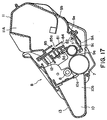
- Figure 17 depicts a structural configuration as a solution to the above described problem of developer packing, according to which an opening 85a, i.e., an exit, is provided, in addition to the opening 84, i.e., the entrance-exit, on the most inward side 85 of the gap between the electrodes 81 and 82, to allow the developer to pass between the electrodes 81 and 82, so that the developer which enters the gap between the two electrodes does not become packed therein.
- an opening 85a i.e., an exit
- the opening 84 i.e., the entrance-exit
- the developer amount detecting portion 80 comprising the first and second electrodes 81 and 82 determines the developer amount by detecting the electrostatic capacity between the two electrodes 81 and 82. Therefore, the positional accuracy of the electrodes is extremely important. Further, since the primary object in this example is to accurately predict the time when toner depletion, which results in various while spots, occurs, the electrodes 81 and 82 should be positioned in the adjacency of the development roller 9a where the developer remains until it is depleted.
- the first and second electrodes 81 and 82 are attached to the development unit frame 12, as shown in Figure 18.
- the means for attaching the first and second electrodes 81 and 82 screws, adhesive, crimping, insert molding, or the like, may be used.
- the electrodes 81 and 82 can be accurately positioned so that the distance between the first and second electrodes 81 and 82 is precisely set. Further, the positioning of the first and second electrodes 81 and 82 in the adjacency of the development roller 9a makes it possible to very closely detect the time when the developer runs out.
- the process cartridge B design may be modified as shown in Figure 20.
- the second electrode 82 is attached to the development unit frame 12
- the first electrode 81 is attached to the front wall 11a of the developer container 11A, so that the first and second electrodes 81 and 82 oppose each other as the development unit frame 12 is joined with the developer container 11A. This arrangement affords more latitude in terms of the frame structure design for the process cartridge B.
- the contact 19 (unillustrated in Figure 5) disposed in the apparatus main assembly 14 makes electrical contact with the contact portion 93a of the electrical contact 93 of the development roller 9a, and as a result, development bias is applied to the development roller 9a from the bias circuit 101.
- the information obtained by the aforementioned developer amount detecting apparatus is displayed on the monitor screen of a user's personal computer or the like, as shown in Figures 23 and 24; a user is informed of the developer amount by observing the point on a gauge 42 indicated by a hand (needle) 41 which moves in accordance with the developer amount.
- the developer amount detection circuit in this embodiment is provided with a contact 91 to be connected with the electrode 17 of the electrophotographic image forming apparatus main assembly 14 to apply voltage to the first electrode 81, and a contact 93 to be connected with the electrode 19 of the apparatus main assembly 14 to apply the development bias to the development roller 9a.
- the separate provision of these contacts 91 and 93 affords more latitude in design.
- the voltage to be applied to the first electrode 81 is provided from the development bias circuit 101, eliminating the need for an additional power source. Therefore, cost increase can be avoided.
- the contacts are in the form of a single piece, and therefore, there is no stray capacitance, assuring that the electrostatic capacity is accurately measured.
- the developer amount in the process cartridge B is accurately determined by continuously detecting the decrease in the amount of the developer between the electrodes 81 and 82, and the "END" of the developer supply in the process cartridge B is accurately detected by detecting the amount of the developer between the development roller 9a and electrode 83.
- the relationship between the developer amount and the output of the toner amount detection circuit is graphically shown in Figure 28, (a), (b) and (c).
- the developing apparatus C in this example is in the form of a cartridge comprising a developer carrier such as a development roller 9a, a development chamber 9A which contains toner to supply the developer carrier with developer, and a plastic development unit frame 11 in which the developer carrier and development chamber 9A are contained.
- the developing apparatus C a cartridge version of the developing apparatus portion of the process cartridge B in the first example and the embodiment described above, that is, a cartridge formed by eliminating the photosensitive drum 7, charging means 8, and cleaning means 10, from the process cartridge B. Therefore, all the descriptions given to the structures of the developing apparatus portion and developer amount detecting means portion, in the first and second embodiments, also apply to the developing apparatus in this embodiment. Thus, the description of the structure and function of the developing apparatus in this embodiment will be omitted here, by referring to the preceding descriptions of the first example and the embodiment.
- the developing apparatus in this example may be provided with the third electrode 83.
- the amount of the remaining developer can be continuously detected while the amount of the remaining developer is in a range from approximately 30 % down to 0 %, provided that the entire amount of the developer contained in the developer container before a process cartridge is put to use for the first time is 100 %.
- the application of the present invention does not need to be limited to the described embodiment.
- modifications may be made so that the amount of the remaining developer in the developer container can be continuously detected in a range from 50 % down to 0 %, or from 40 % down to 0 %.
Landscapes
- Physics & Mathematics (AREA)
- General Physics & Mathematics (AREA)
- Engineering & Computer Science (AREA)
- Computer Vision & Pattern Recognition (AREA)
- Dry Development In Electrophotography (AREA)
- Electrophotography Configuration And Component (AREA)
Description
- The present invention relates to an image developing apparatus, a process cartridge, an electrophotographic image forming apparatus, and a development unit frame.
- An electrophotographic image forming apparatus includes an electrophotographic copying machine, an electrophotographic printer (for example, LED printer, laser beam printer, and the like), an electrophotographic facsimile apparatus, an electrophotographic word processor, and the like.
- A process cartridge is a cartridge which integrally comprises a charging means, a developing meaning or a cleaning means, and an electrophotographic photosensitive member, and is removably installable in the main assembly of an electrophotographic image forming apparatus; or a cartridge which integrally comprises at least a developing means, and an electrophotographic photosensitive member, and is removable installable in the main assembly of an image forming apparatus.
- In the past, an image forming apparatus which employed an electrophotographic image formation process employed a process cartridge system, according to which an electrophotographic photosensitive member, and one or a plurality of processing means which works on the electrophotographic photosensitive member, are integrally assembled in the form of a cartridge removably installable in the main assembly of an image forming apparatus. Also according to this process cartridge system, the maintenance for an image forming apparatus can be performed by a user him/her self; the user does not need to rely on a service person for the maintenance. Therefore, the employment of a process cartridge system drastically improved the operational efficiency of an image forming apparatus. As a result, a process cartridge system has been widely used in the field of the image forming apparatus.
- In the case of an image forming apparatus such as the above described electrophotographic image forming apparatus which employs a process cartridge system, a user him/herself must exchange a cartridge. Therefore, the image forming apparatus is provided with a means for informing the user of developer depletion, for example, an developer amount detecting apparatus.
- In the past, in order to detect the amount of developer remainder; a pair of electrodes in the form of a rod are placed in the developer container of a developing means, and the amount of the developer in the developer container was determined by detecting the changes which occurred to the eletrostatic capacity between the two electrodes.
- Japanese Laid-Open Patent Application No. 100571/1993 discloses a developer amount detecting apparatus, which employs a developer amount detecting member comprising two electrodes placed in the same plane in parallel to each other, one being in the shape of a "U", and the other being in the shape of a "I" so that they can be coupled on the same plane. This developer amount detecting member is located at the bottom portion of the developer container. This development amount detecting apparatus detects the amount of remaining developer by detecting the fluctuation in the electrostatic capacity between the parallel electrodes placed in the same plane.
- However, the above described developer amount detecting apparatus is of a type which detects the presence (absence) of the developer within the developer container. More specifically, it is of a type that detects the developer shortage only immediately before the depletion of the developer within the developer container. In other words, it is not enabled to continuously detect how much developer remained in the developer container.
- Thus, if it is possible to continuously detect the amount of the developer remaining in the developer container, a user can know the state of developer usage in the developer container, which makes it possible for the user to prepare a new process cartridge for exchange. This is very convenient for the user.
- The primary object of the present invention is to provide an image developing apparatus, a process cartridge, and an electrophotographic image forming apparatus, which are capable of continuously detecting the amount of the developer remainder, and a developing apparatus usable for a process cartridge and an electrophotographic image forming apparatus.
- Another object of the present invention is to provide an electrophotographic image forming apparatus, which comprises a developer amount detecting means capable of continuously detecting the amount of the developer remainder in accordance with the consumption of the developer within the developer container, to offer more convenience to a user in terms of usage, as well as a process cartridge, a developing apparatus, and a development unit frame, which are compatible with the above electrophotographic image forming apparatus.
- Another object of the present invention is to provide a development unit frame better designed for improving the aforementioned process cartridge and developing apparatus in terms of quality and assembly efficiency, and also, installing the developer amount detecting means, or the like, capable of continuously detecting the amount of the developer in the development chamber in accordance with the developer consumption, into the aforementioned process cartridge or developing apparatus.
- According to the present invention, there is provided a developing apparatus according to
claim 1, a process cartridge according toclaim 11, and an electrophotographic image forming apparatus according to claim 21. - These and other objects, features and advantages of the present invention will become more apparent upon a consideration of the following description of the preferred embodiments of the present invention taken in conjunction with the accompanying drawings.
-
- Figure 1 is a schematic vertical sectional view of an example of an electrophotographic image forming apparatus, and depicts the general structure thereof.
- Figure 2 is an external perspective view of the electrophotographic image forming apparatus.
- Figure 3 is a vertical cross sectional view of an example of a process cartridge.
- Figure 4 is an external perspective view of the process cartridge of Figure 3 as seen from the bottom side.
- Figure 5 is an external perspective view of the cartridge installation chamber in the main assembly for receiving the process cartridge.
- Figure 6 is a perspective view of the partially disassembled development unit frame, and depicts an example of the structural configuration for connecting electrodes of the developer amount detecting apparatus.
- Figure 7 is a graph which shows the relationship between the toner amount and electrostatic capacity in the developer amount detecting apparatus.
- Figure 8 is a perspective view of the first and second electrodes in the developer amount detecting apparatus.
- Figure 9 is a vertical cross-sectional view of another example of a process cartridge.
- Figure 10 is a vertical cross-sectional view of another example of a process cartridge.
- Figure 11 is a perspective view of the development unit frame, and depicts how the first and second electrodes are attached to the development unit frame.
- Figure 12 is a perspective view of the development unit frame, and depicts another way the first and second electrodes are attached to the development unit frame.
- Figure 13 is a vertical cross-sectional view of a process cartridge, and depicts how the developer is circulated in the development chamber.
- Figure 14 is a vertical cross-sectional view of another process cartridge and depicts how the developer is circulated in the development chamber.
- Figure 15 is a vertical cross-sectional view of the process cartridge of Figure 14 and depicts how the developer is circulated in the development chamber.
- Figure 16 is a vertical cross-sectional view of the process cartridge of Figure 14, and depicts how the developer is circulated in the development chamber.
- Figure 17 is a vertical sectional view of another example of a process cartridge.
- Figure 18 is a perspective view of the development unit frame in the first example, and depicts how the first and second electrodes are attached to the development unit frame.
- Figure 19 is a vertical sectional view of another example of a process cartridge.
- Figure 20 is a vertical sectional view of another example of a process cartridge.
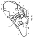
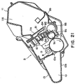
- Figure 21 is a vertical sectional view of another example of a process cartridge.
- Figure 22 is the diagram of the developer amount detection circuit for the developer amount detecting apparatus in the first example.
- Figure 23 is a schematic drawing of an example of a developer amount gauge.
- Figure 24 is a schematic drawing of another example of a developer amount gauge.
- Figure 25 is a vertical sectional view of the process cartridge in another embodiment of the present invention.
- Figure 26 is a longitudinal sectional view of a process cartridge according to an embodiment of the present invention.
- Figure 27 is the diagram of the developer amount detection circuit for the developer amount detecting apparatus according to the present invention.
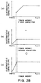
- Figure 28 is a graph which depicts the developer amount detection principle in accordance with the present invention.
- Figure 29 is a vertical cross-sectional view of the process cartridge in another embodiment of the present invention.
- Figure 30 is a vertical sectional view of another example of a developing apparatus equipped with a developer amount detecting apparatus.
- Hereinafter, an image developing apparatus, a process cartridge, an electrophotographic image forming apparatus, and a development unit frame, which are in accordance with the present invention will be described in more detail with reference to the appended drawings.
- First, referring to Figure 1, an example of an electrophotographic image forming apparatus in which a process cartridge is installable will be described. The electrophotographic image forming apparatus in this embodiment is an electrophotographic laser beam printer, which forms images on various recording media, for example, recording paper, OHP sheet, fabric, and the like, with the use of an electrophotographic image formation process.
- A laser beam printer A is provided with an electrophotographic photosensitive member in the form of a drum, that is, a
photosensitive drum 7. Thephotosensitive drum 7 is charged by acharge roller 8, i.e., a charging means. Then, a laser beam modulated with image data is projected onto thephotosensitive drum 7, from anoptical means 1 comprising alaser diode 1a, apolygon mirror 1b, alens 1c, and adeflection mirror 1d. As a result, a latent image is formed on thephotosensitive drum 7 in correspondence to the image data. This latent image is developed into a toner image, i.e., a visible image, by a developingmeans 9. - Referring to Figure 3, which makes it easier to understand the following description, the developing
means 9 is provided with adevelopment chamber 9A in which adevelopment roller 9a as a developer bearing member is disposed. The developer in adeveloper container 11A, as a developer storage portion, located next to thedevelopment chamber 9A is sent to thedevelopment roller 9a by the rotation of adeveloper sending member 9b. In thedevelopment chamber 9A, adeveloper stirring member 9e is disposed adjacent to thedevelopment roller 9a, to circulate the developer in thedevelopment chamber 9A. Thedevelopment roller 9a contains astationary magnet 9c. As thedevelopment roller 9a is rotated, the developer is borne and carried by the peripheral surface of thedevelopment roller 9a. Then, as thedevelopment roller 9a is rotated further, the developer on thedevelopment roller 9a is regulated by adevelopment blade 9d into a developer layer with a predetermined thickness, while being triboelectrically charged, and is delivered to the image developing area. In this image developing area, the developer is transferred from thedevelopment roller 9a onto the latent image on thephotosensitive drum 7. As a result, a toner image is formed on thephotosensitive drum 7. Thedevelopment roller 9a is connected to a development bias circuit so that development bias is applied to thedevelopment roller 9a. Normally, the development bias is compound bias comprising AC voltage and DC voltage. - Meanwhile, a piece of
recording medium 2 is conveyed from a sheet feeder cassette 3a, which stores plural sheets ofrecording medium 2, to an image transfer area by a combination of apickup roller 3b, conveyer roller pairs 3c and 3d, and a registration roller pair 3e, in synchronism with the progress of the toner image formation. In the transfer area, atransfer roller 4 as an image transferring means is disposed, and as voltage is applied to thetransfer roller 4, the toner image on thephotosensitive drum 7 is transferred onto therecording medium 2. - After the transfer, the
recording medium 2 is conveyed to a fixing means 5 along aconveyer guide 3f, and passed through the fixing means 5, which comprises a drivingroller 5c, and a fixingroller 5b containing aheater 5a. As therecording medium 2 is passed through the fixing means 5, the toner image having been transferred onto therecording medium 2 is fixed to therecording medium 2 with the application of heat and pressure from the fixing means 5. - Thereafter, the
recording medium 2 is advanced further, is passed through areversal path 3j, and then, is discharged into adelivery tray 6, bydischarge roller pairs delivery tray 6 is located at the top of themain assembly 14 of the laser beam printer A, i.e., an electrophotographic image forming apparatus. It should be noted here that therecording medium 2 can be discharged from the apparatusmain assembly 14, without going through the reversingpath 3j, by activating aflapper 3k. In such a case, therecording medium 2 is discharged by a discharge roller pair 3m. In this embodiment, theaforementioned pickup roller 3b,conveyer roller pairs conveyance guide 3f, dischargeroller pairs - After the toner image transfer onto the
recording medium 2 by thetransfer roller 4, thephotosensitive drum 7 is cleaned by a cleaning means 10; the developer remaining on thephotosensitive drum 7 is removed by the cleaning means 10. Then, thephotosensitive drum 7 is reused for the following cycle of image formation process. The cleaning means 10 comprises anelastic cleaning blade 10a placed in contact with thephotosensitive drum 7. It scrapes away the toner remaining on thephotosensitive drum 7 from thephotosensitive drum 7, and collects it into awaste toner bin 10b. - Referring to Figure 3, the process cartridge B in this example is an integral assembly of various frames and components therein. In production, a development unit (which makes up the developing apparatus portion) is formed by a welding a
developer storage frame 11 comprising a developer container (developer storage portion) for storing the developer, and adeveloper conveying member 9b, to adevelopment unit frame 12 which holds the developingmeans 9 made up of thedevelopment roller 9a,development blade 9d, and the like. Then, the process cartridge B is completed by integrally uniting this development unit with acleaning unit frame 13 in which thephotosensitive drum 7, the cleaning means 10 made up of thecleaning blade 10a and the like, and thecharger roller 8, are disposed. - The process cartridge B is rendered removably installable in the cartridge installing means with which the
main assembly 14 of an electrophotographic image forming apparatus is provided. The cartridge installing means in this embodiment is made up of a guiding means 13R (13L) formed as a part of the external right (left) wall of the process cartridge B (Figure 4), and guideportions 16R (16L) (Figure 5) formed as a part of the apparatusmain assembly 14, in which the guiding means 13R (13L) is insertable. - Further, the process cartridge B in this example is provided with a developer amount detecting apparatus as a means capable of continuously detecting the amount of the developer remainder in the
development chamber 9A as the developer in thedevelopment chamber 9A is consumed. - Referring to Figure 3, the developer amount detecting apparatus in this example comprises first and second electrically conductive portions (electrodes) 81 and 82, which are measurement electrodes, and are parts of
developer detecting portion 80. Theelectrodes development roller 9a. In order to detect the amount of the developer, voltage is applied to thefirst electrode 81 or thesecond electrode 82 to induce static electricity between theelectrodes electrodes first electrode 81. This process will be described later in detail. - The magnetic developer is attracted to the peripheral surface of the
development roller 9a by themagnetic roller 9c contained in thedeveloper roller 9a, and is borne on the peripheral surface of thedevelopment roller 9a as thedeveloper 9a is rotated. Then, as thedevelopment roller 9a is rotated further, the magnetic developer on thedevelopment roller 9a is scraped by thedevelopment blade 9d. As a result, an even layer of the magnetic developer is formed on the peripheral surface of thedevelopment roller 9a. - The first and
second electrodes development roller 9a enters between them. - The dielectric constant of developer is greater than that of air. Therefore, when there is developer between the first and
second electrodes development chamber 9A, a larger electrostatic capacity is provided between them than when not, because, when a sufficient amount of developer is in thedevelopment chamber 9A, the aforementioned developer scraped away from thedevelopment roller 9a continuously enters between the first andsecond electrodes development chamber 9A is consumed, the amount of the developer which enters between theelectrodes - In order to improve the accuracy with which the developer amount is continuously detected, all that is necessary is to increase the amount of change in the aforementioned electrostatic capacity, by increasing the sizes of the first and
second electrodes second electrodes - Referring to Figure 11 - 18, which will be helpful to better understand this example, the first and
second electrodes development roller 9a. They are formed of electrically conductive material such as stainless steel (BUS), iron, phosphor bronze, aluminum, electrically conductive resin, and the like, which are identical in terms of electrode function. However, in this embodiment, nonmagnetic metallic material such as nonmagnetic SUS was employed to prevent the electrode material from affecting developer circulation. - More specifically, in this example, the
first electrode 81 was formed of nonmagnetic SUS, and was 14 mm in width (W1), and 0.3 mm in thickness (t1). Thesecond electrode 82 was formed of nonmagnetic SUS, and was 17 mm in width (W2), and 0.5 mm in thickness (t2)- Arranging these electrodes along and in parallel to thedevelopment roller 9a in the longitudinal direction produced good results. The configurations of theelectrodes electrodes inward side 85, as shown in Figure 3, provides good results. - Further, in order to increase the surface areas of the
electrodes electrodes first electrode 81 or thesecond electrode 82 may be formed in the form of a round rod as illustrated in Figures 9 and 10, which show the examples of such arrangement, and in which the first and second electrodes, respectively, are in the form of a round rod. Although the number of the rod in the examples illustrated in Figures 9 and 10 is singular, it may be plural. - Next, the positioning of the
electrodes development roller 9a, the first andsecond electrodes narrow electrodes - Next, referring to Figure 13 - 16, the developer circulation within the
development chamber 9A will be described. - When a process cartridge, more specifically, the developing apparatus portion of the process cartridge, is used for the first time, no developer is present between the first and
second electrodes development chamber 9A. In this situation, first, the developer T in thedevelopment chamber 9A is sent toward thedevelopment roller 9a by the stirringmember 9e, and then, is attracted to the peripheral surface of thedevelopment roller 9a Then, as thedevelopment roller 9a is rotated, the developer is borne on the peripheral surface of thedevelopment roller 9a. As thedevelopment roller 9a is rotated further, the developer on the peripheral surface of thedevelopment roller 9a is leveled, that is, the excess amount of the developer on the peripheral surface of thedevelopment roller 9a is scraped away, and as it is scraped away, it enters between the first andsecond electrodes - As the developer T continues to enter into the gap between the first and
second electrodes development chamber 9A is still full of the developer T. Therefore, once the developer T enters the gap through theentrance 84, that is, the bottom side of the gap between theelectrodes development chamber 9A. Therefore, it does not occur until the amount of the developer T in thedevelopment chamber 9A reduces by a substantial amount that the developer T between theelectrodes development chamber 9A, the gap between the first andsecond electrodes - Referring to Figure 15, as the amount of the developer T in the
developer container 11A anddevelopment chamber 9A reduces due to the developer consumption, the portion of the developer which has been blocking the entrance (also, exit) 84 moves away from theentrance 84, allowing the developer T between the first andsecond electrodes development roller 9a by the magnetic fore as it falls, whereas the other may simply fall all the way to join the rest of the developer T in thedevelopment chamber 9A to be supplied again to thedevelopment roller 9a. Also, in certain class the developer T between the two electrodes is caused to directly return to the peripheral surface of thedevelopment roller 9a by the magnetic force. - In the situation illustrated in Figure 15, the amount of the developer in the
development chamber 9A has become small enough to allow the developer between theelectrodes development chamber 9A by an amount sufficient to make it necessary for the developer to be scraped away from thedevelopment roller 9a by thedevelopment blade 9b to be supplied into the gap between the first andsecond electrodes electrodes development chamber 9A. - In the last stage of toner consumption in the process cartridge B, that is, after the developer in the
developer container 11A anddevelopment chamber 9A has been virtually entirely consumed, the developer which remains adjacent to the tip of thedevelopment blade 9d for scraping away the excess amount of the developer layer on the peripheral surface of thedevelopment roller 9a, that is, the developer remaining between thedevelopment roller 9a andfirst electrode 82 is consumed until the developer is completely depleted (END state). During this stage, the resultant prints tend to suffer from white spots. - As is evident from the above description, according to this example, the amount of the developer in the
development chamber 9A is determined by measuring the amount of the developer between the first andsecond electrodes electrodes - Also according to this example, the structure configuration adjacent to the
electrodes second electrodes inward end 85; the gap is provided with only oneopening 84, which serves as the entrance as well as the exit. Therefore, widening the gap between theelectrodes - However, if the amount of the developer scraped away from the peripheral surface of the
development roller 9a by thedevelopment blade 9b per unit of time increases because of the increase in the rotational speed of thedevelopment roller 9a, or the like, the amount of the developer entering between the first andsecond electrodes electrodes electrodes - Figure 17 depicts a structural configuration as a solution to the above described problem of developer packing, according to which an
opening 85a, i.e., an exit, is provided, in addition to theopening 84, i.e., the entrance-exit, on the mostinward side 85 of the gap between theelectrodes electrodes - Next, the structure for attaching the first and
second electrodes - The developer
amount detecting portion 80 comprising the first andsecond electrodes electrodes electrodes development roller 9a where the developer remains until it is depleted. - Thus, in this example, the first and
second electrodes development unit frame 12, as shown in Figure 18. As for the means for attaching the first andsecond electrodes electrodes second electrodes second electrodes development roller 9a makes it possible to very closely detect the time when the developer runs out. - The first and
second electrodes development unit frame 12, and then, are attached thereto with an appropriate means, as described above. However, theelectrodes development unit frame 12 with the use of such a process as vapor deposition or printing, or may be built into thedevelopment unit frame 12, as electrically conductive portions, with the use of a combination of electrically conductive resin and two color molding. Compared to the design in this example in which the electrodes and development unit frame are manufactured independently from each other, these alternative designs are much smaller in terms of attachment error and/or component size error, and therefore, their employment can improve the positioning accuracy for the electrodes. - Further, when necessary, for example, in a case that the
development unit frame 12 is small, the design of the process cartridge B may be modified so that the first andsecond electrodes developer container 11A, as shown in Figure 19. In this case, theelectrodes - Further, the process cartridge B design may be modified as shown in Figure 20. In this case, the
second electrode 82 is attached to thedevelopment unit frame 12, and thefirst electrode 81 is attached to the front wall 11a of thedeveloper container 11A, so that the first andsecond electrodes development unit frame 12 is joined with thedeveloper container 11A. This arrangement affords more latitude in terms of the frame structure design for the process cartridge B. - In the preceding portions of this specification, the structural arrangement for continuously detecting the developer amount was described with reference to a case in which magnetic developer was used as the developer for the process cartridge B. However, the examples are also applicable to various process cartridges comprising a developing apparatus portion which employs nonmagnetic developer.
- In the case of a developing apparatus structure which employs nonmagnetic developer, a
developer coating roller 86 is used as a means for supplying thedevelopment roller 9a with the developer. Theroller 86 is an elastic member formed of sponge or the like, and is rotated in the counter direction to thedevelopment roller 9a, in contact with thedevelopment roller 9a. The developer is coated on thedevelopment roller 9a by the electrostatic force (measured in coulomb) generated by the contact. Immediately prior to the complete depletion of the developer T, the developer T remains above the interface between thedevelopment roller 9a anddeveloper coating roller 86. Thus, positioning the first andsecond electrodes - Next, referring to Figures 4 - 6, this example will be described regarding the structural arrangement for connecting the
electrodes main assembly 14 side. - In this example, the first and
second electrodes projections projections holes 12a and 12b with which thedevelopment unit frame 12 is provided, when the first andsecond electrodes development unit frame 12. - The
development unit frame 12 is provided with aholder 90, which is fixed to-thedevelopment unit frame 12, at one of the longitudinal end. Theholder 90 rotatively supports thedevelopment roller 9a with the interposition of a bearing. Theholder 90 is provided with a firstelectrical contact 91 and a secondelectrical contact 92. Thecontact portions electrical contacts aforementioned projections second electrodes holder 90 is fixed to thedevelopment unit frame 12, at one of the longitudinal ends. - The
contact portions 91b and 92b, that is, the ends opposite to the aforementioned free ends, of the first and secondelectrical contacts holder 90, being exposed from the outward surface of theholder 90 so that, as the process cartridge B is installed into the apparatusmain assembly 14, they become electrically connected to thecontacts 17 and 18 (Figure 5), respectively, positioned in the apparatusmain assembly 14. - With the provision of the above described structural configuration, as the process cartridge B is installed into the
main assembly 14 of an electrophotographic image forming apparatus, voltage is applied from the electrophotographic image forming apparatusmain assembly 14 to thefirst electrode 81 through the firstelectrical contact 91, and the voltage induced in thesecond electrode 82, which is in accordance with the electrostatic capacity between theelectrodes main assembly 14 through the secondelectrical contact 92. Of course, it is possible that voltage be applied from the electrophotographic image forming apparatusmain assembly 14 to thesecond electrode 82 through the firstelectrical contact 91. and the voltage induced in thefirst electrode 81 be outputted to the electrophotographic image forming apparatusmain assembly 14 through the secondelectrical contact 92. - Next, referring to Figure 22, an example of the above described principle in the form of a developer amount detecting apparatus will be described further. Figure 22 is an example of a diagram of a developer amount detection circuit, inclusive of the connection between the circuit and the developer
amount detecting portion 80 provided with the first andsecond electrodes - The detecting
portion 80, which has an electrostatic capacity Ca which fluctuates in accordance with the change in the developer amount, comprises an input electrode as an impedance element, that is, thefirst electrode 81 in this example and an output electrode, that is, thesecond electrode 82 in this example. The input electrode is connected to adevelopment bias circuit 101, as a development bias applying means, through the firstelectrical contact 91, and the output electrode is connected to thecontrol circuit 102 of the developeramount detection circuit 100 through the secondelectrical contact 92. A referential capacity element (Cb) is also connected to thedevelopment bias circuit 101, and establishes a reference voltage V1 for detecting the amount of the remaining developer, with the use of the AC current 11 applied through thebias circuit 101. It is obvious that, as the process cartridge B is installed into the apparatusmain assembly 14, the contact 19 (unillustrated in Figure 5) disposed in the apparatusmain assembly 14 makes electrical contact with thecontact portion 93a of theelectrical contact 93 of thedevelopment roller 9a, and as a result, development bias is applied to thedevelopment roller 9a from thebias circuit 101. - The
control circuit 102 establishes the reference voltage V1 by adding the amount V2 of the voltage drop caused by an AC current I1', that is, a current shunted by a volume VR1 from the AC current 11 applied to the reference impedance element, and a resistor R2, to voltage V3 established by resistors R3 and R4. - Therefore, an AC current 12 applied to the developer
amount detecting portion 80 is inputted into anamplifier 103, and then, is outputted as a voltage V4 (V1 - I2 x R5) which represents the amount of the remaining developer. Then, its output value is used as the value of the detected amount of the remaining developer. - The image forming apparatus in this example prompts a user to prepare a new process cartridge or a developer supply cartridge, by displaying the consumed amount of the developer determined based on the information obtained by continuously detecting the developer amount between the first and
second electrodes - Regarding the method for displaying the developer amount, the information obtained by the aforementioned developer amount detecting apparatus is displayed on the monitor screen of a user's personal computer or the like, as shown in Figures 23 and 24; a user is informed of the developer amount by observing the point on a
gauge 42 indicated by a hand (needle) 41 which moves in accordance with the developer amount. - The image forming apparatus main assembly itself may be provided with a display panel, such as an LED based
display panel 43 shown in Figure 25, which flashes at a position correspondent to the developer amount. - Figure 26 depicts an embodiment of the present invention. The developing apparatus in the process cartridge B in this embodiment is provided with a third electrically conductive portion (electrode) 83 as the measuring member for the developer
amount detecting portion 80. Otherwise, it is substantially the same in structure as the one in the process cartridge B in the first example. Thus, the structures and components in this embodiment which are the same as those in the first example will be given the same reference numbers as those given to the corresponding structures and components in the first example, and their detailed descriptions will be omitted. - In other words, this embodiment is a duplicate of the first example in terms of the first and second electrically conductive portions (electrodes) 81 and 82, their structures and positioning, developer circulation between the
electrodes electrodes electrodes - The primary object of the process cartridge structure in this embodiment is to accurately detect the point in time immediately before the printing errors in the form of white spots begin to be seen in finished prints. All that is necessary to accomplish this object is to detect the developer amount in the area in the process cartridge B, from which the last supply of the developer is consumed. Thus, in this embodiment, the developer amount in the immediate adjacencies of the second and
third electrodes development roller 9a, is detected as described in the description of the first embodiment, regarding the developer circulation. - In other words, in the case of the developer amount detecting apparatus in this embodiment, which is illustrated in Figure 26, not only the first and
second electrodes third electrode 83, is positioned along thedevelopment roller 9a. Thethird electrode 83 is disposed much closer to thedevelopment roller 9a than thefirst electrode 83. - With the provision of the above described structural arrangement, as voltage is applied to the
first electrode 81, static electricity is induced between the first andsecond electrodes development roller 9a andthird electrode 83 by the development bias applied to thedevelopment roller 9a, by an amount of Cc. The development amount is determined by measuring these electrostatic capacities Ca and Cc. - Illustrated in Figure 27 is an example of a developer amount detection circuit in this embodiment. The overall circuit structure is substantially the same as the developer amount detection circuit in the first embodiment given in Figure 22, with one exception that the
third electrode 83 is disposed in a way to oppose thedevelopment roller 9a so that static electricity is induced between thedevelopment roller 9a andthird electrode 83 by the amount of Cc. Therefore, the detailed description for this embodiment will be omitted. - Referring to Figure 27, the developer amount detection circuit in this embodiment is provided with a
contact 91 to be connected with theelectrode 17 of the electrophotographic image forming apparatusmain assembly 14 to apply voltage to thefirst electrode 81, and acontact 93 to be connected with theelectrode 19 of the apparatusmain assembly 14 to apply the development bias to thedevelopment roller 9a. The separate provision of thesecontacts - Further, the voltage to be applied to the
first electrode 81 is provided from thedevelopment bias circuit 101, eliminating the need for an additional power source. Therefore, cost increase can be avoided. - Further, the contacts are in the form of a single piece, and therefore, there is no stray capacitance, assuring that the electrostatic capacity is accurately measured.
- As described above, in this embodiment, the developer amount in the process cartridge B is accurately determined by continuously detecting the decrease in the amount of the developer between the
electrodes development roller 9a andelectrode 83. The relationship between the developer amount and the output of the toner amount detection circuit is graphically shown in Figure 28, (a), (b) and (c). - Again referring to Figure 27, the first electrostatic capacity element (Ca) provided by the first and
second electrodes development roller 9a andthird electrode 83, are connected in parallel, reducing the number of the contacts in the image forming apparatusmain assembly 14 and process cartridge B. Therefore, the process cartridge B in this embodiment is lower in cost. - Lengthy routing of wiring increases the chance that static electricity is induced between the adjacent portions of wiring, which in turn reduces detection accuracy. Thus, reducing the distance electric wiring is routed leads to improvement in detection accuracy. Therefore, the second and
third electrodes third electrodes third electrode 83 is bent so that the bent portion of theelectrode 83 extends away from thesecond electrode 82, reducing the distance between thethird electrode 83 anddevelopment roller 9a as described above. - Figure 30 depicts another example of a developing apparatus cartridge C.
- The developing apparatus C in this example is in the form of a cartridge comprising a developer carrier such as a
development roller 9a, adevelopment chamber 9A which contains toner to supply the developer carrier with developer, and a plasticdevelopment unit frame 11 in which the developer carrier anddevelopment chamber 9A are contained. In other words, the developing apparatus C a cartridge version of the developing apparatus portion of the process cartridge B in the first example and the embodiment described above, that is, a cartridge formed by eliminating thephotosensitive drum 7, charging means 8, and cleaning means 10, from the process cartridge B. Therefore, all the descriptions given to the structures of the developing apparatus portion and developer amount detecting means portion, in the first and second embodiments, also apply to the developing apparatus in this embodiment. Thus, the description of the structure and function of the developing apparatus in this embodiment will be omitted here, by referring to the preceding descriptions of the first example and the embodiment. - Needless to say, the developing apparatus in this example may be provided with the
third electrode 83. - As is evident from the description, according to the present invention, the amount of the remaining developer can be accurately and continuously detected.
- In the described embodiment, the amount of the remaining developer can be continuously detected while the amount of the remaining developer is in a range from approximately 30 % down to 0 %, provided that the entire amount of the developer contained in the developer container before a process cartridge is put to use for the first time is 100 %. However, the application of the present invention does not need to be limited to the described embodiment. For example, modifications may be made so that the amount of the remaining developer in the developer container can be continuously detected in a range from 50 % down to 0 %, or from 40 % down to 0 %. It should be noted here that "0 %" does not means a state of a process cartridge in which the developer has been completely depleted; it also includes another state of a process cartridge in which the amount of the developer in the process cartridge has decreased to a point close enough to disable the image forming apparatus to form images with a predetermined level of quality (development quality).
- As described above, according to the first aspect of the present invention, a developing apparatus, a process cartridge, or an electrophotographic image forming apparatus, comprises: a first electrically conductive portion; a second electrically conductive portion opposing the first electrically conductive portion; a first electrical contact for receiving the voltage to be applied to the first electrically conductive portion, from the electrophotographic image forming apparatus main assembly; a third electrically conductive portion for inducing static electricity between the developer carrying member and itself as voltage is applied to the third electrically conductive portion from the electrophotographic image forming apparatus main assembly; and a second electrical contact for transmitting to the electrophotographic image forming apparatus main assembly, compound electrical signals comprising electrical signals generated in accordance with the electrostatic capacity provided between the first and second electrically conductive portions as voltage is applied to the first electrically conductive portion, and electrical signals generated in accordance with the electrostatic capacity provided between the developer carrying member and third electrically conductive portion as voltage is applied to the developer carrying member, in order to enable the electrophotographic image forming apparatus main assembly to detect the amount of the remaining developer. Therefore, the amount of the remaining developer in the development chamber can be continuously detected as the developer is consumed. Further, the measurement errors, which occur when detecting the amount of the remaining developer on the basis of the fluctuation in the electrostatic capacity between two electrodes, in an unstable ambience, can be eliminated to reduce overall detection error. Therefore, a developing apparatus, a process cartridge, and an electrophotographic image forming apparatus, can be drastically improved in terms of convenience.
- Also, according to the first aspect of the present invention, a development unit frame comprises: a portion for supporting a developer carrying member for conveying developer to an electrophotographic photosensitive member to develop an electrostatic latent image formed on the electrophotographic photosensitive member; a portion for supporting a regulating member which regulates the amount of the developer allowed to remain on the peripheral surface of the developer carrying member; a portion for supporting the first electrically conductive portion; and a portion for supporting the second electrically conductive portion in such a way that the second electrically conductive portion opposes the first electrically conductive portion supported by the first electrically conductive portion supporting portion; and a portion for supporting the third electrically conductive portion in such a way that the third electrically conductive portion opposes the developer carrying member supported by the developer carrying member supporting portion. Therefore, it is assured that a developer amount detecting means or the like, which can continuously detect the amount of the developer remaining in the development chamber as the developer is consumed, is properly attached to the aforementioned developing apparatus, process cartridge, or electrophotographic image forming apparatus.
- As is evident from the above description of the embodiment of the present invention, according to the present invention, it is assured that the amount of the remaining developer can be continuously detected.
- while the invention has been described with reference to the structures disclosed herein, it is not confined to the details set forth and this application is intended to cover such modifications or changes as may come within the scope of the following claims.
Claims (22)
- A developer device (9) for developing an electrostatic latent image formed on an electrophotographic photosensitive member (7), said developer device being mountable to a main assembly (14) of an electrophotographic image forming apparatus, said developer device comprising:a developer carrier member (9a) for feeding a developer to said electrophotographic photosensitive member to develop the electrostatic latent image formed on the electrophotographic photosensitive member;a first electroconductive portion (81);a second electroconductive portion (82) for cooperating with said first electroconductive portion to provide an electrostatic capacity wherein said first electroconductive portion and said second electroconductive portion are disposed such that the developer may enter between them;a first electrical contact (91) for receiving a voltage to be applied to said first electroconductive portion from the main assembly of the electrophotographic image forming apparatus;a developer carrier member electrical contact (93) for receiving a voltage to be applied to said developer carrier member from the main assembly of the image-forming apparatus;a third electroconductive portion (83) for cooperating with said developer carrier member (9a) to provide an electrostatic capacity when a voltage is applied to said developer carrier member from the main assembly of said electrophotographic image-forming apparatus;a second electrical contact (92) for transmitting, to the main assembly of the electrophotographic image forming apparatus, a combined electric signal for permitting the main assembly of the image-forming apparatus to detect the remaining amount of the developer, the combined electric signal being formed ofan electric signal corresponding to an electrostatic capacity between said first electroconductive portion (81) and said second electroconductive portion (82) when a voltage is applied to said first electroconductive portion through said first electric contact (91) andan electric signal corresponding to an electrostatic capacity between said developer carrier member (9a) and the third electroconductive portion when a voltage is applied to said developer carrier member through said developer carrier member electrical contact (93), to detect the remaining amount of the developer in the developer device by the main assembly of the electrophotographic image forming apparatus.
- A developer device according to Claim 1, wherein said first electroconductive portion and second electroconductive portion are arranged in a longitudinal direction of a developer carrier member in the form of a developing roller, wherein said first electroconductive portion is disposed more remote from said developer carrier member than said second electroconductive portion.
- A developer device according to Claim 1 or 2, wherein said second electroconductive portion has one end portion which is bent toward said developer carrier member, and the electrostatic capacity is provided between the bent portion and said developer carrier member.
- A developer device according to Claim 1, claim 2 or claim 3, arranged such, that the developer is fed between said first electroconductive portion and said second electroconductive portion, and is retracted in a direction toward an entering side.
- A developer device according to Claim 1, claim 2 or claim 3, arranged such, that the developer fed between said first electroconductive portion and second electroconductive portion passes between said first electroconductive portion and second electroconductive portion.
- A developer device according to Claim 1, claim 2 or claim 3, wherein said first electroconductive portion and second electroconductive portion have a flat-plate-like shape, and a gap between said first electroconductive portion and second electroconductive portion is wider at a developer entering side.
- A developer device according to Claim 4, further comprising a magnet (9c) disposed in said developer carrier member, and said developer is a magnetic developer which is deposited on the surface of said developer carrier member.
- A developer device according to any one of Claims 1 to 3, wherein said third electroconductive portion is constituted integrally with said second electroconductive portion.
- A developer device according to Claim 8, wherein said third electroconductive portion (83) is at an angle relative to said second electroconductive portion (82)
- A developer device according to Claim 9, wherein said third electroconductive portion is disposed opposed to said developer carrier member, and wherein said third electroconductive portion is disposed closer to said developer carrier member than said first electroconductive portion and said second electroconductive portion.
- A process cartridge (B) detachably mountable to a main assembly (14) of an electrophotographic image forming apparatus, said process cartridge comprising:(a) an electrophotographic photosensitive member(7); and(b) a developer device (9) for developing an electrostatic latent image formed on the electrophotographic photosensitive member, said developer device including;a developer carrier member (9a) for feeding a developer to said electrophotographic photosensitive member to develop the electrostatic latent image formed on the electrophotographic photosensitive member;
a first electroconductive portion (81);
a second electroconductive portion (82) for cooperating with said first electroconductive portion to provide an electrostatic capacity, wherein said first electroconductive portion and said second electroconductive portion are disposed such that developer may enter between them;
a first electrical contact (91) for receiving a voltage to be applied to said first electroconductive portion from the main assembly of the electrophotographic image forming apparatus;
a developer carrier member electrical contact (93) for receiving a voltage from the main assembly of the image-forming apparatus;
a third electroconductive portion (93) for cooperating with said developer carrier member (9a) to provide an electrostatic capacity when a voltage is applied to said developer carrier member from the main assembly of said electrophotographic image forming apparatus;
a second electrical contact (92) for transmitting, to the main assembly of the electrophotographic image forming apparatus, a combined electric signal for permitting the main assembly of the image-forming apparatus to detect the remaining amount of the developer, the combined electric signal being formed of
an electric signal corresponding to an electrostatic capacity between said first electroconductive portion (81) and said second electroconductive portion (82) when a voltage is applied to said first electroconductive portion through said first electrical contact and
an electric signal corresponding to an electrostatic capacity between said developer carrier member and the third electroconductive portion when a voltage is applied to said developer carrier member through said developer carrier member electrical contact, to detect the remaining amount of the developer in the process cartridge by the main assembly of the electrophotographic image forming apparatus. - A process cartridge according to Claim 11, wherein said first electroconductive portion and second electroconductive portion are arranged in a longitudinal direction of a developer carrier member in the form of a developing roller, and wherein said first electroconductive portion is disposed more remote from said developer carrier member than said second electroconductive portion.
- A process cartridge according to Claim 11, wherein said second electroconductive portion has one end portion which is bent toward said developer carrier member, and the electrostatic capacity is provided between the bent portion and said developer carrier member.
- A process cartridge according to Claim 11, Claim 12 or Claim 13, wherein the developer is fed between said first electroconductive portion and said second electroconductive portion, and the developer fed to between said first electroconductive portion and said second electroconductive portion is retracted in a direction toward an entering side.
- A process cartridge according to Claim 11, Claim 12 or Claim 13, arranged such, that the developer fed between said first electroconductive portion and second electroconductive portion passes between said first electroconductive portion and second electroconductive portion.
- A process cartridge according to Claim 11, Claim 12 or Claim 13, wherein said first electroconductive portion and second electroconductive portion have a flat-plate-like shape, and the gap between said first electroconductive portion and second electroconductive portion is wider at a developer entering side.
- A process cartridge according to Claim 14, further comprising a magnet (9c) disposed in said developer carrier member, and said developer is a magnetic developer which is deposited on the surface of said developer carrier member.
- A process cartridge according to any one of Claims 11 to 13, wherein said third electroconductive portion is constituted integrally with said second electroconductive portion.
- A process cartridge according to Claim 18, wherein said third electroconductive portion is at an angle relative to said second electroconductive portion.
- A process cartridge according to Claim 19, wherein said third electroconductive portion is disposed opposed to said developer carrier member, and wherein said third electroconductive portion is disposed closer to said developer carrier member than said first electroconductive portion and said second electroconductive portion.
- An electrophotographic image forming apparatus for forming an image on a recording material, to which a process cartridge (B) is detachably mountable, said apparatus comprising:(i) mounting means (16R, 16L) for mounting the process cartridge, which includes:an electrophotographic photosensitive member (7); and a developer device (9) for developing an electrostatic latent image formed on the electrophotographic photosensitive member, said developer device including;a developer carrier member (9a) for feeding a developer to said electrophotographic photosensitive member to develop the electrostatic latent image formed on the electrophotographic photosensitive member;a first electroconductive portion (81);a second electroconductive portion (82) for cooperating with said first electroconductive portion to provide an electrostatic capacity wherein said first electroconductive portion and said second electroconductive portion are disposed such that the developer may enter between them;a first electrical contact (91) for receiving a voltage to be applied to said first electroconductive portion from the main assembly of the electrophotographic image forming apparatus;a developer carrier member electrical contact (93) for receiving a voltage to be applied to said developer carrier member from the main assembly of the image-forming apparatus;a third electroconductive portion (83) for cooperating with said developer carrier member to provide an electrostatic capacity when a voltage is applied to said developer carrier member from the main assembly of said electrophotographic image forming apparatus;a second electrical contact (92) for transmitting, to the main assembly of the electrophotographic image forming apparatus, a combined electric signal for permitting the main assembly of the image-forming apparatus to detect the remaining amount of the developer in the process cartridge, the combined electric signal being formed ofan electric signal corresponding to an electrostatic capacity between said first electroconductive portion and said second electroconductive portion when a voltage is applied to said first electroconductive portion through said first electrical contact andan electric signal corresponding to an electrostatic capacity between said developer carrier member and the third electroconductive portion when a voltage is applied to said developer carrier member through said developer carrier member electrical contact, to detect the remaining amount of the developer in the process cartridge by the main assembly of the electrophotographic image forming apparatus; and(ii) detecting means (80, 100) for detecting in substantially real time the amount of a developer existing in said process cartridge on the basis of the electric signal transmitted from said second electrical contact.
- An electrophotographic image forming apparatus according to Claim 21, wherein said developer amount detecting means is arranged to detect in substantially real time the amount of said developer in said process cartridge, and to display the result of the detection continuously.
Applications Claiming Priority (2)
| Application Number | Priority Date | Filing Date | Title |
|---|---|---|---|
| JP37383498 | 1998-12-28 | ||
| JP37383498 | 1998-12-28 |
Publications (3)
| Publication Number | Publication Date |
|---|---|
| EP1016939A2 EP1016939A2 (en) | 2000-07-05 |
| EP1016939A3 EP1016939A3 (en) | 2001-05-30 |
| EP1016939B1 true EP1016939B1 (en) | 2006-02-01 |
Family
ID=18502839
Family Applications (1)
| Application Number | Title | Priority Date | Filing Date |
|---|---|---|---|
| EP99310455A Expired - Lifetime EP1016939B1 (en) | 1998-12-28 | 1999-12-22 | Image developing apparatus, process cartridge, electrophotographic image forming apparatus, and development unit frame |
Country Status (7)
| Country | Link |
|---|---|
| US (2) | US6859627B2 (en) |
| EP (1) | EP1016939B1 (en) |
| KR (1) | KR100363808B1 (en) |
| CN (1) | CN1165818C (en) |
| AU (1) | AU6553099A (en) |
| CA (1) | CA2293188C (en) |
| DE (1) | DE69929667T2 (en) |
Families Citing this family (33)
| Publication number | Priority date | Publication date | Assignee | Title |
|---|---|---|---|---|
| US6859627B2 (en) * | 1998-12-28 | 2005-02-22 | Canon Kabushiki Kaisha | Image developing apparatus, process cartridge, electrophotographic image forming apparatus, and developing unit frame |
| US6912366B1 (en) * | 1999-08-31 | 2005-06-28 | Canon Kabushiki Kaisha | Image forming apparatus comprising means for detecting an amount of developer contained in a developer container, a memory for storing the amount detected by the detecting means, and control means for updating the information stored in the memory |
| JP3720671B2 (en) * | 2000-04-06 | 2005-11-30 | キヤノン株式会社 | Developing device, process cartridge, and electrophotographic image forming apparatus |
| US6946988B2 (en) * | 2000-11-10 | 2005-09-20 | Simple Devices | Detachable remote controller for an electronic entertainment device and a method for using the same |
| JP3697168B2 (en) * | 2001-03-09 | 2005-09-21 | キヤノン株式会社 | Process cartridge and electrophotographic image forming apparatus |
| US6785479B2 (en) | 2001-12-28 | 2004-08-31 | Canon Kabushiki Kaisha | Image forming apparatus having a control section for detecting an amount of developer and an amount detection method of developer of image forming apparatus |
| JP2003255806A (en) | 2002-02-28 | 2003-09-10 | Canon Inc | Process cartridge, developing device, and image forming apparatus |
| JP3848191B2 (en) * | 2002-03-25 | 2006-11-22 | キヤノン株式会社 | Developing device, process cartridge, and electrophotographic image forming apparatus |
| JP2003302825A (en) * | 2002-04-09 | 2003-10-24 | Canon Inc | Developing device, process cartridge and image forming apparatus |
| JP2004205950A (en) * | 2002-12-26 | 2004-07-22 | Canon Inc | Cleaning device, process cartridge, and image forming apparatus |
| JP3858875B2 (en) * | 2003-08-25 | 2006-12-20 | 村田機械株式会社 | Developer and image forming apparatus having the same |
| JP4110143B2 (en) * | 2004-01-30 | 2008-07-02 | キヤノン株式会社 | Electrophotographic image forming apparatus, unit detachable from electrophotographic image forming apparatus, and process cartridge |
| JP4095589B2 (en) * | 2004-02-27 | 2008-06-04 | キヤノン株式会社 | Electrophotographic image forming apparatus and process cartridge |
| US20050267518A1 (en) * | 2004-04-07 | 2005-12-01 | Tiax, Llc | Tourniquet and method of using same |
| JP4963363B2 (en) * | 2006-03-01 | 2012-06-27 | キヤノン株式会社 | Image forming apparatus and developer remaining amount detection method |
| JP4804212B2 (en) * | 2006-04-19 | 2011-11-02 | キヤノン株式会社 | Process cartridge, electrophotographic image forming apparatus, process cartridge production method and reproduction method |
| US7764887B2 (en) * | 2006-04-26 | 2010-07-27 | Ricoh Company, Limited | Developing device and image forming apparatus |
| CN200941842Y (en) * | 2006-05-25 | 2007-09-05 | 周光真 | Multi-functional helmet |
| US7555231B2 (en) * | 2006-09-14 | 2009-06-30 | Lexmark International, Inc. | Capacitive toner level sensor and methods of use |
| JP4667444B2 (en) | 2006-12-13 | 2011-04-13 | キヤノン株式会社 | Electrophotographic image forming apparatus |
| JP5506236B2 (en) | 2009-04-30 | 2014-05-28 | キヤノン株式会社 | Cartridge and electrophotographic image forming apparatus |
| TWI442195B (en) | 2009-12-16 | 2014-06-21 | Canon Kk | Process cartridge, photosensitive drum unit, developing unit and electrophotographic image forming apparatus |
| JP5862165B2 (en) | 2011-09-29 | 2016-02-16 | ブラザー工業株式会社 | Image forming apparatus |
| JP5906743B2 (en) | 2012-01-05 | 2016-04-20 | ブラザー工業株式会社 | Image forming apparatus |
| US9250567B2 (en) | 2013-07-12 | 2016-02-02 | Canon Kabushiki Kaisha | Developer container for detecting developer amount based on capacitance, developing apparatus, process cartridge, and image forming apparatus |
| JP6468747B2 (en) * | 2013-09-24 | 2019-02-13 | キヤノン株式会社 | Developer container, developing device, process cartridge, and image forming apparatus |
| JP6138181B2 (en) | 2014-04-15 | 2017-05-31 | キヤノン株式会社 | Resin molded product and cartridge used for image forming apparatus, method for manufacturing movable member used for image forming apparatus, and method for manufacturing cartridge |
| US9535398B2 (en) | 2014-09-04 | 2017-01-03 | Canon Kabushiki Kaisha | Developer cartridge, developing apparatus, process cartridge and image forming apparatus |
| JP6444210B2 (en) * | 2015-02-23 | 2018-12-26 | キヤノン株式会社 | Developer container, developing device, process cartridge, developer container forming method, developing device forming method, process cartridge forming method |
| JP6855284B2 (en) | 2017-03-03 | 2021-04-07 | キヤノン株式会社 | Cartridge and image forming device |
| US10466617B2 (en) * | 2017-12-19 | 2019-11-05 | Lexmark International, Inc. | Capacitive toner level sensor |
| US10969730B2 (en) | 2019-02-25 | 2021-04-06 | Canon Kabushiki Kaisha | Image forming apparatus and image forming unit |
| JP7205361B2 (en) * | 2019-04-17 | 2023-01-17 | 株式会社リコー | Toner amount detection device, toner amount detection method, toner amount detection program |
Family Cites Families (48)
| Publication number | Priority date | Publication date | Assignee | Title |
|---|---|---|---|---|
| US4133453A (en) * | 1975-12-18 | 1979-01-09 | Tokyo Shibaura Electric Co., Ltd. | Toner residual amount detecting device |
| JPS57154268A (en) * | 1981-03-19 | 1982-09-24 | Oki Electric Ind Co Ltd | Detector for remaining amount of developer |
| JPS58126556A (en) * | 1982-01-23 | 1983-07-28 | Canon Inc | Developing device |
| JPH01180379A (en) * | 1988-01-12 | 1989-07-18 | Nec Corp | Printer device |
| US5003917A (en) * | 1988-08-12 | 1991-04-02 | Minolta Camera Kabushiki Kaisha | Developing apparatus with image quality control |
| JPH02197880A (en) * | 1989-01-27 | 1990-08-06 | Canon Inc | Developer detection device |
| JPH03200989A (en) * | 1989-10-04 | 1991-09-02 | Canon Inc | Image forming device |
| US5623328A (en) | 1990-04-27 | 1997-04-22 | Canon Kabushiki Kaisha | Process cartridge and image forming system on which process cartridge is mountable |
| US5828928A (en) | 1990-04-27 | 1998-10-27 | Canon Kabushiki Kaisha | Process cartridge mountable in an image forming system and a method for assembling a cleaning device |
| US5294960A (en) | 1990-11-06 | 1994-03-15 | Canon Kabushiki Kaisha | Detachable two-frame process cartridge for an image forming apparatus |
| US5229821A (en) | 1990-11-30 | 1993-07-20 | Canon Kabushiki Kaisha | Process cartridge with toner depletion detection feature and image forming apparatus using the same |
| JP2899123B2 (en) | 1991-03-20 | 1999-06-02 | キヤノン株式会社 | Charging member, charging device, image forming apparatus provided with this charging device, and process unit detachable from this image forming device |
| JPH04355477A (en) * | 1991-05-31 | 1992-12-09 | Canon Inc | Image forming device |
| JP3255175B2 (en) | 1991-10-03 | 2002-02-12 | キヤノン株式会社 | Toner presence detection device |
| DE69223383T2 (en) | 1991-11-20 | 1998-04-16 | Canon Kk | Method of attaching a squeegee blade, work unit and imaging device |
| US5585895A (en) | 1991-12-19 | 1996-12-17 | Canon Kabushiki Kaisha | Developing device and process cartridge with it |
| JP3005130B2 (en) | 1992-01-10 | 2000-01-31 | キヤノン株式会社 | Charging device, image forming apparatus, and process cartridge |
| DE69320842T2 (en) | 1992-01-30 | 1999-03-04 | Canon Kk | Charging part, charging device, process cartridge and image forming device |
| JP3126532B2 (en) | 1992-02-10 | 2001-01-22 | キヤノン株式会社 | Cleaning device, process cartridge, and image forming apparatus |
| JP3259985B2 (en) | 1992-09-04 | 2002-02-25 | キヤノン株式会社 | Process cartridge and image forming apparatus |
| EP0586042B1 (en) | 1992-09-04 | 1998-09-02 | Canon Kabushiki Kaisha | Process cartridge and image forming apparatus |
| EP0586041B1 (en) | 1992-09-04 | 1997-03-19 | Canon Kabushiki Kaisha | Electrophotographic process cartridge and image forming apparatus with such process cartridge |
| EP0586044B1 (en) | 1992-09-04 | 1997-03-26 | Canon Kabushiki Kaisha | Process cartridge, method for assembling process cartridge and image forming apparatus |
| JPH06161242A (en) * | 1992-11-17 | 1994-06-07 | Canon Inc | Developing device |
| US5966566A (en) | 1993-03-24 | 1999-10-12 | Canon Kabushiki Kaisha | Recycle method for process cartridge and image forming apparatus |
| EP0843231B1 (en) | 1993-07-30 | 2001-10-31 | Canon Kabushiki Kaisha | Charging member, charging device and process cartridge detachably mountable to image forming apparatus |
| CA2128676C (en) | 1993-09-08 | 1997-12-23 | John D. Sotack | Capacitive sensor |
| JPH08179625A (en) | 1994-12-21 | 1996-07-12 | Canon Inc | Process cartridge and image forming device |
| US5943528A (en) | 1995-04-28 | 1999-08-24 | Canon Kabushiki Kaisha | Toner accommodating container with a gripping cover feature usable with a process cartridge, a process cartridge using the same, and an apparatus using the process cartridge |
| JP3268162B2 (en) | 1995-04-28 | 2002-03-25 | キヤノン株式会社 | Process cartridge and image forming apparatus |
| JP3294465B2 (en) | 1995-04-28 | 2002-06-24 | キヤノン株式会社 | Process cartridge and image forming apparatus |
| JP3154642B2 (en) | 1995-04-28 | 2001-04-09 | キヤノン株式会社 | Process cartridge, method for coupling toner developing frame and cleaning frame, and image forming apparatus |
| JP3774488B2 (en) | 1995-04-28 | 2006-05-17 | キヤノン株式会社 | Process cartridge and image forming apparatus |
| JPH0916056A (en) | 1995-06-30 | 1997-01-17 | Canon Inc | Process cartridge and image forming device |
| JP3372719B2 (en) | 1995-07-11 | 2003-02-04 | キヤノン株式会社 | Process cartridge and image forming apparatus |
| US5768658A (en) | 1995-07-21 | 1998-06-16 | Canon Kabushiki Kaisha | Electrode member, developing apparatus, process cartridge and image forming apparatus |
| US5768660A (en) | 1995-08-02 | 1998-06-16 | Canon Kabushiki Kaisha | Charging device and process cartridge |
| JP3445040B2 (en) * | 1995-10-09 | 2003-09-08 | キヤノン株式会社 | Image forming device |
| JP3869877B2 (en) | 1996-01-09 | 2007-01-17 | キヤノン株式会社 | Electrophotographic image forming apparatus, process cartridge, and developing device |
| JPH09211960A (en) | 1996-01-29 | 1997-08-15 | Canon Inc | Process cartridge and image forming device |
| JP3372747B2 (en) | 1996-02-09 | 2003-02-04 | キヤノン株式会社 | Developing device |
| JP3382465B2 (en) | 1996-07-04 | 2003-03-04 | キヤノン株式会社 | Process cartridge and electrophotographic image forming apparatus |
| JP3323749B2 (en) | 1996-08-01 | 2002-09-09 | キヤノン株式会社 | Magnetic sealing device, developing device, and image forming device |
| JP3563893B2 (en) | 1996-10-30 | 2004-09-08 | キヤノン株式会社 | Image forming apparatus and cartridge |
| US5987269A (en) * | 1998-02-13 | 1999-11-16 | Hewlett-Packard Company | Toner quantity measuring technique in an electrophotographic printer |
| JP3530751B2 (en) | 1998-10-09 | 2004-05-24 | キヤノン株式会社 | Process cartridge and electrophotographic image forming apparatus |
| JP3530752B2 (en) | 1998-10-09 | 2004-05-24 | キヤノン株式会社 | Electrophotographic image forming apparatus, process cartridge, developing device, developer supply container, and measuring component |
| US6859627B2 (en) * | 1998-12-28 | 2005-02-22 | Canon Kabushiki Kaisha | Image developing apparatus, process cartridge, electrophotographic image forming apparatus, and developing unit frame |
-
1999
- 1999-12-22 US US09/469,517 patent/US6859627B2/en not_active Expired - Lifetime
- 1999-12-22 DE DE69929667T patent/DE69929667T2/en not_active Expired - Lifetime
- 1999-12-22 EP EP99310455A patent/EP1016939B1/en not_active Expired - Lifetime
- 1999-12-24 CA CA002293188A patent/CA2293188C/en not_active Expired - Fee Related
- 1999-12-24 AU AU65530/99A patent/AU6553099A/en not_active Abandoned
- 1999-12-28 KR KR1019990063214A patent/KR100363808B1/en not_active IP Right Cessation
- 1999-12-28 CN CNB991229916A patent/CN1165818C/en not_active Expired - Lifetime
-
2004
- 2004-09-07 US US10/934,416 patent/US7095967B2/en not_active Expired - Fee Related
Also Published As
| Publication number | Publication date |
|---|---|
| US7095967B2 (en) | 2006-08-22 |
| CN1267842A (en) | 2000-09-27 |
| US20050025508A1 (en) | 2005-02-03 |
| CN1165818C (en) | 2004-09-08 |
| KR20000057109A (en) | 2000-09-15 |
| US20020012542A1 (en) | 2002-01-31 |
| DE69929667D1 (en) | 2006-04-13 |
| EP1016939A3 (en) | 2001-05-30 |
| CA2293188C (en) | 2002-12-10 |
| DE69929667T2 (en) | 2006-08-10 |
| KR100363808B1 (en) | 2002-12-11 |
| AU6553099A (en) | 2000-07-20 |
| US6859627B2 (en) | 2005-02-22 |
| EP1016939A2 (en) | 2000-07-05 |
| CA2293188A1 (en) | 2000-06-28 |
Similar Documents
| Publication | Publication Date | Title |
|---|---|---|
| EP1016939B1 (en) | Image developing apparatus, process cartridge, electrophotographic image forming apparatus, and development unit frame | |
| US6804475B2 (en) | Process cartridge comprising grounding, charging bias, and developing bias contacts and input and output contacts, and electrophotographic image forming apparatus to which the process cartridge is detachably mountable | |
| US6892035B2 (en) | Developing device, a process cartridge, and an electrophotographic image forming apparatus for detecting an amount of developer | |
| KR100630988B1 (en) | Electrophotographic image forming apparatus, process cartridge, developing device, developer supply container and measuring part therefor | |
| CA2285157C (en) | Electrophotographic image forming apparatus, process cartridge, developing device and measuring part | |
| EP1117015B1 (en) | Process cartridge and image forming apparatus | |
| JP2001092335A (en) | Process cartridge, electrophotographic image forming device and developer quantity detection member | |
| JP3848191B2 (en) | Developing device, process cartridge, and electrophotographic image forming apparatus | |
| EP1083464A2 (en) | Developing apparatus, process cartridge, feeding member and an elastic sheet | |
| JP3897504B2 (en) | Developing device, process cartridge, and electrophotographic image forming apparatus | |
| JP3984759B2 (en) | Developing device, process cartridge, and electrophotographic image forming apparatus | |
| AU782688B2 (en) | Image developing apparatus, process cartridge, electrophotographic image forming apparatus, and development unit frame | |
| JP2001117344A (en) | Developing device, process cartridge, electrophotographic image forming device and developing frame | |
| JP2001125464A (en) | Process cartridge, electrophotographic image forming device, developing device, developer amount detecting device, and developer rest detecting member | |
| JP2003195619A (en) | Developing device, process cartridge, and image forming apparatus | |
| JP2005121762A (en) | Developing device, processing cartridge, and electrophotographic image forming apparatus | |
| JP2001125463A (en) | Process cartridge, electrophotographic image forming device, developing device, developer amount detecting device, and developer rest detecting member | |
| JP2001125378A (en) | Developing device, process cartridge and electrophotographic image forming device |
Legal Events
| Date | Code | Title | Description |
|---|---|---|---|
| PUAI | Public reference made under article 153(3) epc to a published international application that has entered the european phase |
Free format text: ORIGINAL CODE: 0009012 |
|
| AK | Designated contracting states |
Kind code of ref document: A2 Designated state(s): CH DE FR GB IT LI |
|
| AX | Request for extension of the european patent |
Free format text: AL;LT;LV;MK;RO;SI |
|
| PUAL | Search report despatched |
Free format text: ORIGINAL CODE: 0009013 |
|
| AK | Designated contracting states |
Kind code of ref document: A3 Designated state(s): AT BE CH CY DE DK ES FI FR GB GR IE IT LI LU MC NL PT SE |
|
| AX | Request for extension of the european patent |
Free format text: AL;LT;LV;MK;RO;SI |
|
| 17P | Request for examination filed |
Effective date: 20011015 |
|
| AKX | Designation fees paid |
Free format text: CH DE FR GB IT LI |
|
| 17Q | First examination report despatched |
Effective date: 20040302 |
|
| GRAP | Despatch of communication of intention to grant a patent |
Free format text: ORIGINAL CODE: EPIDOSNIGR1 |
|
| GRAS | Grant fee paid |
Free format text: ORIGINAL CODE: EPIDOSNIGR3 |
|
| GRAA | (expected) grant |
Free format text: ORIGINAL CODE: 0009210 |
|
| AK | Designated contracting states |
Kind code of ref document: B1 Designated state(s): CH DE FR GB IT LI |
|
| PG25 | Lapsed in a contracting state [announced via postgrant information from national office to epo] |
Ref country code: LI Free format text: LAPSE BECAUSE OF FAILURE TO SUBMIT A TRANSLATION OF THE DESCRIPTION OR TO PAY THE FEE WITHIN THE PRESCRIBED TIME-LIMIT Effective date: 20060201 Ref country code: IT Free format text: LAPSE BECAUSE OF FAILURE TO SUBMIT A TRANSLATION OF THE DESCRIPTION OR TO PAY THE FEE WITHIN THE PRESCRIBED TIME-LIMIT;WARNING: LAPSES OF ITALIAN PATENTS WITH EFFECTIVE DATE BEFORE 2007 MAY HAVE OCCURRED AT ANY TIME BEFORE 2007. THE CORRECT EFFECTIVE DATE MAY BE DIFFERENT FROM THE ONE RECORDED. Effective date: 20060201 Ref country code: CH Free format text: LAPSE BECAUSE OF FAILURE TO SUBMIT A TRANSLATION OF THE DESCRIPTION OR TO PAY THE FEE WITHIN THE PRESCRIBED TIME-LIMIT Effective date: 20060201 |
|
| REG | Reference to a national code |
Ref country code: GB Ref legal event code: FG4D |
|
| REG | Reference to a national code |
Ref country code: CH Ref legal event code: EP |
|
| REF | Corresponds to: |
Ref document number: 69929667 Country of ref document: DE Date of ref document: 20060413 Kind code of ref document: P |
|
| REG | Reference to a national code |
Ref country code: CH Ref legal event code: PL |
|
| ET | Fr: translation filed | ||
| PLBE | No opposition filed within time limit |
Free format text: ORIGINAL CODE: 0009261 |
|
| STAA | Information on the status of an ep patent application or granted ep patent |
Free format text: STATUS: NO OPPOSITION FILED WITHIN TIME LIMIT |
|
| 26N | No opposition filed |
Effective date: 20061103 |
|
| PGFP | Annual fee paid to national office [announced via postgrant information from national office to epo] |
Ref country code: FR Payment date: 20131227 Year of fee payment: 15 |
|
| REG | Reference to a national code |
Ref country code: FR Ref legal event code: ST Effective date: 20150831 |
|
| PG25 | Lapsed in a contracting state [announced via postgrant information from national office to epo] |
Ref country code: FR Free format text: LAPSE BECAUSE OF NON-PAYMENT OF DUE FEES Effective date: 20141231 |
|
| PGFP | Annual fee paid to national office [announced via postgrant information from national office to epo] |
Ref country code: GB Payment date: 20181221 Year of fee payment: 20 |
|
| PGFP | Annual fee paid to national office [announced via postgrant information from national office to epo] |
Ref country code: DE Payment date: 20190228 Year of fee payment: 20 |
|
| REG | Reference to a national code |
Ref country code: DE Ref legal event code: R071 Ref document number: 69929667 Country of ref document: DE |
|
| REG | Reference to a national code |
Ref country code: GB Ref legal event code: PE20 Expiry date: 20191221 |
|
| PG25 | Lapsed in a contracting state [announced via postgrant information from national office to epo] |
Ref country code: GB Free format text: LAPSE BECAUSE OF EXPIRATION OF PROTECTION Effective date: 20191221 |