EP1014332A2 - Control device for a liquid crystal display apparatus - Google Patents
Control device for a liquid crystal display apparatus Download PDFInfo
- Publication number
- EP1014332A2 EP1014332A2 EP99310529A EP99310529A EP1014332A2 EP 1014332 A2 EP1014332 A2 EP 1014332A2 EP 99310529 A EP99310529 A EP 99310529A EP 99310529 A EP99310529 A EP 99310529A EP 1014332 A2 EP1014332 A2 EP 1014332A2
- Authority
- EP
- European Patent Office
- Prior art keywords
- signal
- liquid crystal
- crystal display
- frequency
- period
- Prior art date
- Legal status (The legal status is an assumption and is not a legal conclusion. Google has not performed a legal analysis and makes no representation as to the accuracy of the status listed.)
- Granted
Links
Images


Classifications
-
- G—PHYSICS
- G09—EDUCATION; CRYPTOGRAPHY; DISPLAY; ADVERTISING; SEALS
- G09G—ARRANGEMENTS OR CIRCUITS FOR CONTROL OF INDICATING DEVICES USING STATIC MEANS TO PRESENT VARIABLE INFORMATION
- G09G3/00—Control arrangements or circuits, of interest only in connection with visual indicators other than cathode-ray tubes
- G09G3/20—Control arrangements or circuits, of interest only in connection with visual indicators other than cathode-ray tubes for presentation of an assembly of a number of characters, e.g. a page, by composing the assembly by combination of individual elements arranged in a matrix no fixed position being assigned to or needed to be assigned to the individual characters or partial characters
- G09G3/34—Control arrangements or circuits, of interest only in connection with visual indicators other than cathode-ray tubes for presentation of an assembly of a number of characters, e.g. a page, by composing the assembly by combination of individual elements arranged in a matrix no fixed position being assigned to or needed to be assigned to the individual characters or partial characters by control of light from an independent source
- G09G3/36—Control arrangements or circuits, of interest only in connection with visual indicators other than cathode-ray tubes for presentation of an assembly of a number of characters, e.g. a page, by composing the assembly by combination of individual elements arranged in a matrix no fixed position being assigned to or needed to be assigned to the individual characters or partial characters by control of light from an independent source using liquid crystals
-
- G—PHYSICS
- G09—EDUCATION; CRYPTOGRAPHY; DISPLAY; ADVERTISING; SEALS
- G09G—ARRANGEMENTS OR CIRCUITS FOR CONTROL OF INDICATING DEVICES USING STATIC MEANS TO PRESENT VARIABLE INFORMATION
- G09G3/00—Control arrangements or circuits, of interest only in connection with visual indicators other than cathode-ray tubes
- G09G3/20—Control arrangements or circuits, of interest only in connection with visual indicators other than cathode-ray tubes for presentation of an assembly of a number of characters, e.g. a page, by composing the assembly by combination of individual elements arranged in a matrix no fixed position being assigned to or needed to be assigned to the individual characters or partial characters
- G09G3/34—Control arrangements or circuits, of interest only in connection with visual indicators other than cathode-ray tubes for presentation of an assembly of a number of characters, e.g. a page, by composing the assembly by combination of individual elements arranged in a matrix no fixed position being assigned to or needed to be assigned to the individual characters or partial characters by control of light from an independent source
- G09G3/3406—Control of illumination source
-
- G—PHYSICS
- G09—EDUCATION; CRYPTOGRAPHY; DISPLAY; ADVERTISING; SEALS
- G09G—ARRANGEMENTS OR CIRCUITS FOR CONTROL OF INDICATING DEVICES USING STATIC MEANS TO PRESENT VARIABLE INFORMATION
- G09G2320/00—Control of display operating conditions
- G09G2320/02—Improving the quality of display appearance
- G09G2320/0247—Flicker reduction other than flicker reduction circuits used for single beam cathode-ray tubes
-
- G—PHYSICS
- G09—EDUCATION; CRYPTOGRAPHY; DISPLAY; ADVERTISING; SEALS
- G09G—ARRANGEMENTS OR CIRCUITS FOR CONTROL OF INDICATING DEVICES USING STATIC MEANS TO PRESENT VARIABLE INFORMATION
- G09G2320/00—Control of display operating conditions
- G09G2320/04—Maintaining the quality of display appearance
- G09G2320/041—Temperature compensation
-
- G—PHYSICS
- G09—EDUCATION; CRYPTOGRAPHY; DISPLAY; ADVERTISING; SEALS
- G09G—ARRANGEMENTS OR CIRCUITS FOR CONTROL OF INDICATING DEVICES USING STATIC MEANS TO PRESENT VARIABLE INFORMATION
- G09G2320/00—Control of display operating conditions
- G09G2320/04—Maintaining the quality of display appearance
- G09G2320/043—Preventing or counteracting the effects of ageing
-
- G—PHYSICS
- G09—EDUCATION; CRYPTOGRAPHY; DISPLAY; ADVERTISING; SEALS
- G09G—ARRANGEMENTS OR CIRCUITS FOR CONTROL OF INDICATING DEVICES USING STATIC MEANS TO PRESENT VARIABLE INFORMATION
- G09G2320/00—Control of display operating conditions
- G09G2320/06—Adjustment of display parameters
- G09G2320/0626—Adjustment of display parameters for control of overall brightness
- G09G2320/064—Adjustment of display parameters for control of overall brightness by time modulation of the brightness of the illumination source
Definitions
- the present invention relates to a liquid crystal display (LCD) apparatus which is employed as a display apparatus incorporated in an information processing apparatus, an audio-video apparatus, an advertising indicator, etc. Furthermore, the present invention also relates to an electronic device for providing a control signal to the LCD apparatus.
- LCD liquid crystal display
- a typical LCD apparatus employs a cold cathode ray tube as a light source for illuminating the display panel from the back, and the light source is driven by a light source driving circuit.
- the method for controlling the brightness in the display panel can generally be classified into two types of methods. One is a current-based light modulation method wherein the luminance is controlled by varying a current amplitude of the cold cathode ray tube. The other is a chopping light modulation method wherein the light source is alternately turned ON/OFF at a high speed based on a light modulation signal, and the luminance is virtually controlled by changing the duty ratio which is a ratio between an ON period and an OFF period of the light source.
- the chopping method can accurately control the luminance over a wide brightness range.
- the frequency of flashing of the light used for the light modulation is apt to cause an interference with the driving frequency of the liquid crystal display device.
- flicker in the display and/or moving stripes are perceived on the screen.
- Japanese Laid-Open Publication No. 4-143722 discloses a backlight and a control method thereof.
- a light modulation signal generation circuit 21 is provided in a stage preceding a light source driving circuit 26 for driving a cold cathode ray tube 2 .
- the frequency of the light modulation signal of the light source driving circuit 26 is adjusted so that the shift-number and a shift direction factor of light/dark portions on the screen are slightly offset.
- a control device shown in Figure 13 includes a duty control circuit 15 and a monostable multivibrator 11 coupled via an OR circuit 12 to a light source driving circuit 16 for driving a fluorescent lamp 2 which acts as a backlight of a liquid crystal display panel 1 .
- the fluorescent lamp 2 is turned ON/OFF based on a rectangular wave signal whose duty cycle is variable.
- the rectangular wave signal is synchronized with a signal obtained by dividing a frequency of an image synchronization signal for a liquid crystal screen by an integer n (n>0).
- a light modulation signal frequency Fb and a driving frequency Ff of an LCD apparatus are set independent of each other. Therefore, even when a value suitable for the light modulation signal frequency Fb is determined by way of calculation, there remains a difficulty in regulating the driving frequency Ff and the light modulation signal frequency Fb with high accuracy while maintaining a desirable relationship therebetween. Furthermore, even when these frequencies are initially set to appropriate values, respectively, aging of the LCD device, temperature variation, etc., may cause a frequency-shift. whereby flicker in the display is perceived on the screen.
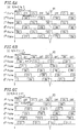
- Prior Art 2 Japanese Laid-Open Publication No. 3-64895 discloses a method for synchronizing the light modulation signal with the liquid crystal driving signal as shown in Figure 13.
- the frequency of the light modulation signal Prior Art 2 only describes "a signal corresponding to an image synchronization signal whose frequency is divided by an integer n equal to or greater than zero.”
- Prior Art 2 fails to disclose specifically what type of signal the image synchronization signal is, and what number is optimal for the integer n. Therefore, even when a light modulation signal is obtained by suitably dividing the frequency of a horizontal synchronization signal having a driving cycle of one horizontal line or a display data latch pulse, which are used as liquid crystal driving signals, flicker in the display may be generated in many cases.
- a liquid crystal display apparatus includes a liquid crystal display device; a light source for illuminating the liquid crystal display device; a LCD device driving circuit for providing a driving voltage to the liquid crystal display device based on a display data signal and a plurality of liquid crystal driving signals including a display data latch signal; a dividing circuit for dividing a frequency of the display data latch signal by a factor of N so as to obtain a period which is N times as large as that of the display data latch signal, where N is an integer greater than zero; a duty control circuit for changing an ON duty ratio of the frequency-divided signal by using the frequency-divided signal as a reference frequency; and a light source driving circuit for turning the light source ON/OFF based on a signal from the duty control circuit having the ON duty ratio set in the duty control circuit, wherein, where a driving duty is (1/D), and a remainder of D divided by the integer N is A, each of the integer N and the value D is set to an integer greater than zero which sati
- a liquid crystal display apparatus includes a liquid crystal display device; a light source for illuminating the liquid crystal display device; a LCD device driving circuit for providing a driving voltage to the liquid crystal display device based on a display data signal and a plurality of liquid crystal driving signals; a dividing circuit for dividing a frequency of a horizontal synchronization signal having a period of one horizontal period, to obtain a period which is N times as large as that of the a horizontal synchronization signal, where N is an integer greater than zero; a duty control circuit for changing an ON duty ratio of the frequency-divided signal by using the frequency-divided signal as a reference frequency; and a light source driving circuit for turning the light source ON/OFF based on a signal from the duty control circuit having the ON duty ratio set in the duty control circuit, wherein where a period of the vertical synchronization signal is M times as large as a period of the horizontal synchronization signal, and a remainder of M divided by N is A, each of the integer N and
- a liquid crystal display apparatus includes a liquid crystal display device; a light source for illuminating the liquid crystal display device; a LCD device driving circuit for providing a driving voltage to the liquid crystal display device based on a display data signal and a plurality of liquid crystal driving signals including a display data latch signal; a dividing circuit for dividing a frequency of the display data latch signal or a horizontal synchronization signal having a cycle of one horizontal period, to obtain a period which is M times as large as that of the display data latch signal or the horizontal synchronization signal, where M is an integer greater than zero; a duty control circuit for changing an ON duty ratio of the frequency-divided signal by using the frequency-divided signal as a reference frequency; and a light source driving circuit for turning the light source ON/OFF based on a signal from the duty control circuit having the ON duty ratio set in the duty control circuit, wherein, where a period of the display data latch signal or the horizontal synchronization signal is tLP, and a rising edge
- a liquid crystal display apparatus includes a liquid crystal display device; a light source for illuminating the liquid crystal display device; a LCD device driving circuit for providing a driving voltage to the liquid crystal display device based on a display data signal and a liquid crystal driving signal having a frame period T1; a duty control circuit for changing an ON duty ratio of a signal having a period T2; a light source driving circuit for turning the light source ON/OFF based on a signal having the ON duty ratio set in the duty control circuit, wherein, where a remainder of T1 divided by T2 is A, the division-number is set to an integer greater than zero which satisfies the following expression: -1 ⁇ ⁇ (T2/A)-2 ⁇ ⁇ 1.
- an electronic device for providing a control signal for use in a liquid crystal display apparatus wherein, where a driving duty ratio is 1/D, a division-number of a display data latch signal to be used in the liquid crystal display apparatus is an integer N, and a remainder of D divided by the division-number N is A, each of the division-number N and the value D is set to an integer greater than zero which satisfies the following expression: -1 ⁇ ⁇ (N/A)-2 ⁇ ⁇ 1.
- an electronic device for providing a control signal for use in a liquid crystal display apparatus wherein, where a division-number of a horizontal synchronization signal having a cycle of one horizontal period is an integer N, a cycle of a vertical synchronization signal to be used in the liquid crystal display apparatus is M times as large as that of a horizontal synchronization signal, and a remainder of the value M divided by the division-number N is A, each of the division-number N and the value M are set to an integer greater than zero which satisfies the following expression: -1 ⁇ ⁇ (N/A)-2 ⁇ ⁇ 1.
- an electronic device for providing a control signal for use in a liquid crystal display apparatus wherein, where a period of a display data latch signal or a horizontal synchronization signal having a cycle of one horizontal period to be used in the liquid crystal display apparatus is tLP, and a rising edge of a light modulation signal with respect to the beginning of a frame period is offset by (B ⁇ tLP), the value B is set to an integer greater than zero which satisfies the following expression: -1 ⁇ ⁇ (M/B)-2 ⁇ ⁇ 1.
- an electronic device for providing a control signal for use in a liquid crystal display apparatus, wherein, where a frame period of the liquid crystal display apparatus is T1, a signal having an ON duty ratio to be changed has a period T2, and a remainder of T1 divided by T2 is A, the electronic device outputs the control signal while setting a division-number to an integer greater than zero which satisfies the following expression: -1 ⁇ ⁇ (T2/A)-2 ⁇ ⁇ 1.
- the frequency of a display data latch signal for driving the liquid crystal display device or the frequency of a horizontal synchronization signal having a cycle of one horizontal period is divided by division-number N by a dividing circuit, and the frequency-divided signal is output to a duty control circuit.
- the duty control circuit changes the ON duty ratio of the frequency-divided signal, and outputs a signal having a modified duty ratio to a light source driving circuit. Based on the signal from the duty control circuit, the light source driving circuit drives the light source for illuminating the liquid crystal display device.
- the light source is turned ON/OFF for each frame (i.e., with the frame frequency).
- the frame frequency is typically equal to or greater than 60 Hz. With such a high frequency, flicker in the display is not perceived by the human eye because the cycle of flashing is extremely fast. Accordingly, light for the display can be appropriately modulated.
- the light modulation signal synchronizes with the fluctuated frequency because the light modulation signal is obtained by dividing the frequency of a liquid crystal display device driving signal.
- a stable driving operation can be carried out independent of such frequency fluctuation. Accordingly, the light for the display is consistently maintained in a suitable state while flicker in the display is reduced.
- the dividing circuit divides the frequency of a display data latch signal or the frequency of a horizontal synchronization signal having a period of "tLP" by a division-number M.
- a rising edge of the light modulation signal is offset with respect to the beginning of a frame period by (B ⁇ tLP) for each frame.
- the value B is set so as to satisfy the following expression: -1 ⁇ ⁇ (M/B)-2 ⁇ ⁇ 1.
- the light source is turned ON/OFF for each frame based on a frame frequency in a manner similar to that under condition 1.
- the value B can be set independent of the relationship between the division-number M and the driving duty ratio. Accordingly, flicker in the display can be reduced under a wider variety of conditions.
- the invention described herein makes possible the advantage of providing an LCD apparatus capable of suppressing the generation of flicker in the display and capable of maintaining a stable display with reduced flicker even when the driving frequency and/or the light modulation signal frequency fluctuate due to aging of the LCD apparatus and/or temperature variation.
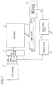
- FIG. 1 is a block diagram showing a liquid crystal display (LCD) apparatus according to Embodiment 1 of the present invention.
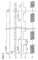
- FIG. 2 is a timing chart showing signals used in an operation of the LCD apparatus according to Embodiment 1 of the present invention.
- Figure 3 is a circuit diagram showing an exemplary configuration of a dividing circuit of the LCD apparatus according to Embodiment 1 of the present invention.
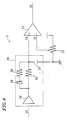
- Figure 4 is a circuit diagram showing an exemplary configuration of a duty control circuit of the LCD apparatus according to Embodiment 1 of the present invention.
- FIG. 5 is a timing chart showing signals used for an operation of the duty control circuit of the LCD apparatus according to Embodiment 1 of the present invention.
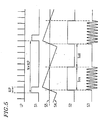
- FIGS 6A through 6C each illustrate principles for suppressing flicker in the display according to the present invention.
- FIG. 7 is a block diagram showing an LCD apparatus according to Embodiment 2 of the present invention.
- Figure 8 is a circuit diagram showing an exemplary configuration of a dividing circuit of the LCD apparatus according to Embodiment 2 of the present invention.
- Figure 9 is a timing chart showing signals used for an operation of a dividing circuit of the LCD apparatus according to Embodiment 2 of the present invention.
- FIG. 10 is a block diagram showing an LCD apparatus according to Embodiment 3 of the present invention.
- FIG 11 is a block diagram showing an LCD apparatus according to Embodiment 4 of the present invention.
- Figure 12 is a block diagram showing a back light according to Prior Art 1.
- FIG. 13 is a block diagram showing an LCD apparatus according to Prior Art 2.
- a liquid crystal display (LCD) apparatus according to Embodiment 1 of the present invention will be described with reference to Figures 1 through 6C .
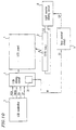
- An LCD apparatus is a simple matrix type LCD apparatus which includes, as shown in Figure 1 , a liquid crystal display panel 1 (hereinafter, referred to as the "LCD panel 1"), a light source 2 such as a cold cathode ray tube for illuminating the LCD panel 1 , a liquid crystal display device driving circuit 3 (hereinafter, referred to as the “LCD device driving circuit 3 "), a dividing circuit 4 , a duty control circuit 5 , a light source driving circuit 6 , and an LCD controller 7 .
- a liquid crystal display panel 1 hereinafter, referred to as the "LCD panel 1”
- a light source 2 such as a cold cathode ray tube for illuminating the LCD panel 1
- a liquid crystal display device driving circuit 3 hereinafter, referred to as the "LCD device driving circuit 3 "
- a dividing circuit 4 hereinafter, referred to as the "LCD device driving circuit 3 "
- a duty control circuit 5 a light source driving circuit 6
- the LCD controller 7 provides a display data signal DATA, and liquid crystal driving signals such as a display data transfer clock XCK, a scan start signal YD, a display data latch signal LP, and the like.
- the LCD device driving circuit 3 outputs a driving voltage to the LCD panel 1 based on the liquid crystal driving signals.
- the dividing circuit 4 divides the frequency of the display data latch signal LP by a division-number N (N is an integer greater than zero).
- the duty control circuit 5 changes an ON duty ratio of the frequency-divided signal from the dividing circuit 4 using the frequency of the frequency-divided signal as a reference frequency.
- the light source driving circuit 6 turns ON/OFF the light source based on the ON duty ratio set by the duty control circuit 5 .
- a simple matrix type LCD apparatus is typically driven by using the scan start signal YD and the display data latch signal LP .
- tLP represents a period of the display data latch signal LP .
- (1/D) is called the driving duty ratio (where D is not required to be equal to the number of dots in the vertical direction of the LCD apparatus, and is freely set to an integer as long as it satisfies the relationship D ⁇ V).
- the dividing circuit 4 divides the frequency of the display data latch signal LP to output a signal S1 having a period of (N ⁇ tLP) to the duty control circuit 5 (N is an integer greater than zero).
- the duty control circuit 5 changes the ON duty of the signal S1 to output a signal S2 having an ON duty of ⁇ Ton/(N ⁇ tLP) ⁇ to the light source driving circuit 6 .
- the light source driving circuit 6 it turned ON/OFF its output voltage to be provided to the light source 2 based on the signal S2 (see signal S3 ).
- the light source 2 is alternately switched between emission and non-emission states at a period of (N ⁇ tLP).
- flicker in the display can be reduced by setting the division-number N by a switch section 46 ( Figure 3 ) so as to satisfy Expression (1): -1 ⁇ ⁇ (N/A)-2 ⁇ ⁇ 1 where A represents the remainder of D/N.
- the division-number N is set to be a value which satisfies the following Expression (3): D/(1+m) ⁇ N ⁇ 3D/(1-3m)
- FIG. 3 shows an exemplary configuration of the dividing circuit 4 .
- the dividing circuit 4 includes counters 41 and 42 , a flip-flop 43 , inverter circuits 44 and 45 , and a switch section 46 for setting the division-number N.
- the division-number N is initially set with binary values through the switches 46 .
- the counter 42 outputs a pulse from its carry output RCO .
- the flip-flop 43 Based on the output pulse, the flip-flop 43 generates a signal S1 having a period of (NxtLPn), as shown in Figure 2 .
- FIG. 4 shows an exemplary configuration of the duty control circuit 5 .
- the duty control circuit 5 includes a low-pass filter circuit 58 , a variable resistor 53 , and a comparator 51 .
- the low-pass filter circuit 58 includes a buffer 52 , a diode 56 , resistors 54 and 55 , and a condenser 57 .
- the comparator 51 Upon receiving a DC voltage S5 set by the variable resistor 53 and a signal S4 output from the low-pass filter circuit 58 , the comparator 51 compares these signals with each other, and outputs the comparison result as a signal S2 .
- the low-pass filter circuit 58 Upon receiving the signal S1 having a period of (N ⁇ tLP), which has been obtained by dividing the frequency of the display data latch signal LP by the division-number N, the low-pass filter circuit 58 generates a triangular wave S4 , and outputs the triangular wave S4 to the comparator 51 .
- the comparator 51 compares the triangular wave S4 with the DC voltage S5 set by the variable resistor 53 . Based on the comparison result, the comparator 51 generates the signal S2 , which is high during a period wherein the triangular wave S4 exceeds the DC voltage S5 .
- the ON duty of the signal S2 can be changed by adjusting the DC voltage S5 .
- the light source driving circuit 6 Upon receiving the signal S2 , the light source driving circuit 6 outputs a voltage as shown as the signal S3 to the light source 2 .
- the light source 2 operates based on the signal S3 , i.e., alternately switched between emission and non-emission states at a period of (N ⁇ tLP).
- flicker in the display can be reduced by setting the division-number N at a value which satisfies Expression (1).
- the principle of flicker reduction will be described with reference to Figures 6A through 6C .
- Figures 6A through 6C each illustrate a flashing operation of the backlight of the LCD apparatus when it is controlled based on the chopping light modulation method.
- Figures 6A through 6C respectively correspond to the following three cases; (a) (N/A)-2 ⁇ 0; (b) (N/A) -2 ⁇ -1; and (c) (N/A)-2 > +1.
- Each of Figures 6A through 6C illustrates "ON-OFF" pattern of 1st to 6th frames.
- the backlight is turned ON/OFF for every frame, and flashing occurs at any point on the screen.
- flashing is not perceived by the human eye because the LCD apparatus is typically operated at a frame frequency which is equal to or greater than 60 Hz. Therefore, the display with reduced flicker can be realized.
- a liquid crystal driving signal is also used as a light modulation signal. Accordingly, the relationship expressed by Expression (1) does not vary after the division-number is once set to a predetermined value, even when the reference frequency is varied due to temperature variations and/or aging of the LCD device. Thus, a stable display with reduced flicker can be realized.
- the LCD apparatus according to Embodiment 2 has a configuration generally the same as that of Embodiment 1 , except that the internal structure of a dividing circuit 10 , and except that the dividing circuit 10 also receives the scan start signal YD in addition to the display data latch signal LP .
- Figure 8 shows a particular, exemplary configuration of the dividing circuit 10 .
- the dividing circuit 10 includes another circuit including a flip-flop 81 , a shift register 82 , a selector 83 , and a light source driving circuit 84 .
- the other details as to the configuration of the dividing circuit 10 is same as those described in Embodiment 1 .
- the scan start signal YD received by the dividing circuit 10 is provided to the flip-flop 81 and the shift register 82 which is composed of B flip-flops.
- the flip-flop 81 divides the frequency of the signal YD so as to obtain a signal S10 having a 1/2 frequency of the signal YD .
- the shift register 82 shifts the signal YD through B stages by using the display data latch signal LP as a clock, outputting the shifted signal as a signal S11 .
- the selector 83 Upon receiving the signals S10 and S11 , if the signal S10 is High, the selector 83 outputs the scan start signal YD from a terminal Y ; whereas, if the signal S10 is Low, the selector 83 outputs the signal S11 from the terminal Y as a signal S12 .
- the signal S12 output from the terminal Y is inverted by the light source driving circuit 84 and output to clear terminals CLR of the counters 41 and 42 .
- the frequency of the display data latch signal LP is divided by the division-number M set by the switch section 46 , thereby generating an output signal S1 having the frequency of (M ⁇ tLP), as shown in Figure 9 .
- the signal S1 is provided to the duty control circuit 5 , as shown in Figure 7 .
- the duty control circuit 5 changes the ON duty of the signal S1 , to generate a signal S2 having the ON duty of ⁇ Ton/(M ⁇ tLP) ⁇ , as shown in Figure 9 , and outputs the signal S2 to the light source driving circuit 6 .
- the light source driving circuit 6 turns ON/OFF the output to the light source 2 based on the signal S2 , as illustrated by the signal S3 in Figure 9 .
- the light source 2 is alternately switched its emission and non-emission states at the period of (M ⁇ tLP).
- the value B can be set independent of the relationship between the division-number M and the driving duty of the display data latch signal or the horizontal synchronization signal.
- flicker in the display can be reduced under a wider variety of conditions.
- the scan start signal YD and the scan start signal S12 which is shifted from the signal YD by (B ⁇ tLP) are used alternately for every two frames, the present invention is not limited to such a case. Needless to say, a rising edge of the signal with respect to the beginning of a frame may be offset by (B ⁇ tLP) with respect to the beginning of the previous frame while setting the value B so as to satisfy Expression ( 8 ).
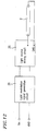
- Embodiment 3 of the present invention will now be described with reference to Figure 10 .
- the components which are identical with those used in Embodiment 1 will not be described herein.
- the alternating signal generation circuit 31 which is typically employed in a simple matrix type LCD, divides the frequency of the display data latch signal LP by a predetermined number of counts, thereby generating a signal S1 and outputting the signal S1 to the duty control circuit 5 .
- the alternating signal generation circuit 31 provides the alternating signal as a light modulation signal to the duty control circuit 5 . Accordingly, a dividing circuit can be omitted. In this case, since the period of the alternating signal can be determined independent of the flashing of the backlight, it is only required to regulate the driving duty ratio of 1/D so that predetermined conditions are satisfied.
- Embodiments 1-3 Although the simple matrix type LCD apparatus has been described in Embodiments 1-3, the present invention is not limited thereto.
- An active matrix type LCD apparatus for example, may be employed as long as it includes a backlight.
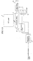
- Embodiment 4 of the present invention is now described with reference to Figure 11 , in which an active matrix type LCD panel is employed.
- some of the signals provided from a controller 7 to an LCD device driving circuit 3 are different from those used in Embodiment 1 ( Figure 1 ).
- a vertical synchronization signal Vsync and a horizontal synchronization signal Hsync are used in place of the scan start signal YD and the display data latch signal LP, respectively.
- the LCD device driving circuit 3 further receives a data enable signal ENAB from a controller 7 .
- the dividing circuit 4 receives the horizontal synchronization signal Hsync and the data enable signal ENAB , and divides the frequency of the horizontal synchronization signal Hsync by the data enable signal ENAB to generate a signal S1 . Subsequent operations of Embodiment 4 are same as those of Embodiment 1 .
- a light source which is employed as a backlight is not limited to the cold cathode ray tubes.
- a light emitting element such as a light emitting diode, an electroluminescent device, or the like, also can be used as the light source as long as light emitted therefrom can be modulated by controlling ON and OFF states of the light source.
- the driving duty of the LCD apparatus rarely changes from the predetermined value during a normal operation.
- the division-number N is manually set through the switches in the dividing circuit as shown in Embodiment 1, the present invention is not limited thereto.
- the division-number N may be calculated in any automatic manner so as to satisfy Expression (1). In such a case, light can be modulated while reducing flicker in the display even when the driving duty varies.
- a dividing circuit, a duty control circuit, and components pertinent thereto in the LCD apparatus is not essential to the present invention. Therefore, any arrangement can be employed within the scope of the present invention. For example, all of those circuits may be incorporated in the LCD apparatus, or may be incorporated in the light source driving circuit.
- the present invention has been described using an LCD apparatus as an example, the present invention is not limited thereto.
- the principle of the present invention is applicable to an electronic apparatus for providing a control signal for use in the LCD apparatus.
- the division-number N is set so as to satisfy the following expression: -1 ⁇ ⁇ (N/A) -2 ⁇ ⁇ 1.
- the frequency of the display data latch signal or the horizontal synchronization signal is divided by the division-number M by a dividing circuit so as to obtain a period of tLP, and a rising edge of a light modulation signal with respect to the beginning of the frame period is offset by (B ⁇ tLP) for every frame.
- the value B is set so as to satisfy the following expression: -1 ⁇ ⁇ (M/B)-2 ⁇ ⁇ 1.
- the state of the light source is switched between ON and OFF for each frame at the frame frequency. Therefore, light can be optimally modulated while reducing flicker in the display perceived by the human eye.
- the light modulation signal synchronizes with the fluctuated frequency.
- the light source can be driven in a stable manner free from any effect from such frequency fluctuation of the LCD driving signals. Accordingly, the display of the LCD panel with reduced flicker can be appropriately maintained.
- the present invention provides the light modulation over a wide brightness range, which is a major feature of the chopping light modulation method.
- the horizontal synchronization signal Hsync is divided to be used as a light modulation signal, thereby reducing flicker in the display of an active matrix type LCD apparatus.
- the value B can be set independent of the relationship between the division-number M of the display data latch signal or a horizontal synchronization signal and the driving duty, whereby flicker reduction can be realized under a wider variety of conditions.
- flicker in the display can be reduced without a dividing circuit, by using a signal having a period T1 and a signal having a period T2.
- the electronic apparatus sets the division-number N so as to satisfy the following expression: -1 ⁇ ⁇ (N/A)-2 ⁇ ⁇ 1
- the division-number N and the value M are set so as to satisfy the following expression: -1 ⁇ ⁇ (N/A)-2 ⁇ ⁇ 1.
- a display data latch signal or a horizontal synchronization signal is divided by a division-number M through a dividing circuit so as to obtain a period of tLP, a rising edge of a light modulation signal with respect to the beginning of a frame period is offset by (B ⁇ tLP) at every frame, and the value B is set so as to satisfy the following expression: -1 ⁇ ⁇ (M/B)-2 ⁇ ⁇ 1.
- a division-number N is set so as to satisfy the following expression: -1 ⁇ ⁇ (T2/A)-2 ⁇ ⁇ 1.
- the light source used in the LCD apparatus is turned ON/OFF at a frame frequency within each frame. Accordingly, a light provided to the LCD apparatus can be modulated so that flicker is not perceived by the human eye.
Landscapes
- Engineering & Computer Science (AREA)
- Physics & Mathematics (AREA)
- Computer Hardware Design (AREA)
- General Physics & Mathematics (AREA)
- Theoretical Computer Science (AREA)
- Chemical & Material Sciences (AREA)
- Crystallography & Structural Chemistry (AREA)
- Liquid Crystal Display Device Control (AREA)
- Control Of Indicators Other Than Cathode Ray Tubes (AREA)
- Liquid Crystal (AREA)
- Devices For Indicating Variable Information By Combining Individual Elements (AREA)
Abstract
Description
Claims (8)
- A liquid crystal display apparatus, comprising:a liquid crystal display device;a light source for illuminating the liquid crystal display device;a LCD device driving circuit for providing a driving voltage to the liquid crystal display device based on a display data signal and a plurality of liquid crystal driving signals including a display data latch signal;a dividing circuit for dividing a frequency of the display data latch signal by a factor of N so as to obtain a period which is N times as large as that of the display data latch signal, where N is an integer greater than zero;a duty control circuit for changing an ON duty ratio of the frequency-divided signal by using the frequency-divided signal as a reference frequency; anda light source driving circuit for turning the light source ON/OFF based on a signal from the duty control circuit having the ON duty ratio set in the duty control circuit, whereinwhere a driving duty ratio is (1/D), and a remainder of D divided by the integer N is A, each of the integer N and the value D is set to an integer greater than zero which satisfies the following expression:
- A liquid crystal display apparatus, comprising:a liquid crystal display device;a light source for illuminating the liquid crystal display device;a LCD device driving circuit for providing a driving voltage to the liquid crystal display device based on a display data signal and a plurality of liquid crystal driving signals;a dividing circuit for dividing a frequency of a horizontal synchronization signal having a period of one horizontal period, to obtain a period which is N times as large as that of the a horizontal synchronization signal, where N is an integer greater than zero;a duty control circuit for changing an ON duty ratio of the frequency-divided signal by using the frequency-divided signal as a reference frequency; anda light source driving circuit for turning the light source ON/OFF based on a signal from the duty control circuit having the ON duty ratio set in the duty control circuit, whereinwhere a period of the vertical synchronization signal is M times as large as a period of the horizontal synchronization signal, and a remainder of M divided by N is A, each of the integer N and the value M is set to an integer greater than zero which satisfies the following expression:
- A liquid crystal display apparatus, comprising:a liquid crystal display device;a light source for illuminating the liquid crystal display device;a LCD device driving circuit for providing a driving voltage to the liquid crystal display device based on a display data signal and a plurality of liquid crystal driving signals including a display data latch signal;a dividing circuit for dividing a frequency of the display data latch signal or a horizontal synchronization signal having a cycle of one horizontal period, to obtain a period which is M times as large as that of the display data latch signal or the horizontal synchronization signal, where M is an integer greater than zero;a duty control circuit for changing an ON duty ratio of the frequency-divided signal by using the frequency-divided signal as a reference frequency; anda light source driving circuit for turning the light source ON/OFF based on a signal from the duty control circuit having the ON duty ratio set in the duty control circuit, whereinwhere a period of the display data latch signal or the horizontal synchronization signal is tLP, and a rising edge of a light modulation signal with respect to the beginning of a frame period is offset by (B×tLP), the value B is set to an integer greater than zero which satisfies the following expression:
- A liquid crystal display apparatus, comprising:a liquid crystal display device;a light source for illuminating the liquid crystal display device;a LCD device driving circuit for providing a driving voltage to the liquid crystal display device based on a display data signal and a liquid crystal driving signal having a frame period T1;a duty control circuit for changing an ON duty ratio of a signal having a period T2;a light source driving circuit for turning the light source ON/OFF based on a signal having the ON duty ratio set in the duty control circuit, whereinwhere a remainder of T1 divided by T2 is A, the division-number is set to an integer greater than zero which satisfies the following expression:
- An electronic device for providing a control signal for use in a liquid crystal display apparatus, wherein
where a driving duty ratio is 1/D, a division-number of a display data latch signal to be used in the liquid crystal display apparatus is an integer N, and a remainder of D divided by the division-number N is A, each of the division-number N and the value D is set to an integer greater than zero which satisfies the following expression: - An electronic device for providing a control signal for use in a liquid crystal display apparatus, wherein
where a division-number of a horizontal synchronization signal having a cycle of one horizontal period is an integer N, a cycle of a vertical synchronization signal to be used in the liquid crystal display apparatus is M times as large as that of a horizontal synchronization signal, and a remainder of the value M divided by the division-number N is A, each of the division-number N and the value M are set to an integer greater than zero which satisfies the following expression: - An electronic device for providing a control signal for use in a liquid crystal display apparatus, wherein
where a period of a display data latch signal or a horizontal synchronization signal having a cycle of one horizontal period to be used in the liquid crystal display apparatus is tLP, and a rising edge of a light modulation signal with respect to the beginning of a frame period is offset by (B×tLP), the value B is set to an integer greater than zero which satisfies the following expression: - An electronic device for providing a control signal for use in a liquid crystal display apparatus, wherein
where a frame period of the liquid crystal display apparatus is T1, a signal having an ON duty ratio to be changed has a period T2, and a remainder of T1 divided by T2 is A, the electronic device outputs the control signal while setting a division-number to an integer greater than zero which satisfies the following expression:
Applications Claiming Priority (4)
| Application Number | Priority Date | Filing Date | Title |
|---|---|---|---|
| JP36804498 | 1998-12-24 | ||
| JP36804498 | 1998-12-24 | ||
| JP34146499 | 1999-11-30 | ||
| JP11341464A JP2000241796A (en) | 1998-12-24 | 1999-11-30 | Liquid crystal display device and electronic equipment outputting control signal of liquid crystal display device |
Publications (3)
| Publication Number | Publication Date |
|---|---|
| EP1014332A2 true EP1014332A2 (en) | 2000-06-28 |
| EP1014332A3 EP1014332A3 (en) | 2000-09-06 |
| EP1014332B1 EP1014332B1 (en) | 2008-02-20 |
Family
ID=26576973
Family Applications (1)
| Application Number | Title | Priority Date | Filing Date |
|---|---|---|---|
| EP99310529A Expired - Lifetime EP1014332B1 (en) | 1998-12-24 | 1999-12-23 | Control device for a liquid crystal display apparatus |
Country Status (5)
| Country | Link |
|---|---|
| US (1) | US6429839B1 (en) |
| EP (1) | EP1014332B1 (en) |
| JP (1) | JP2000241796A (en) |
| KR (1) | KR100354794B1 (en) |
| TW (1) | TW528998B (en) |
Cited By (5)
| Publication number | Priority date | Publication date | Assignee | Title |
|---|---|---|---|---|
| EP1213699A2 (en) | 2000-11-30 | 2002-06-12 | Hitachi, Ltd. | Backlight control for a liquid crystal display device |
| EP1489590A1 (en) * | 2002-03-28 | 2004-12-22 | Matsushita Electric Industries Co., Ltd. | Liquid crystal display device |
| EP1198160A3 (en) * | 2000-10-12 | 2008-11-12 | Hitachi, Ltd. | Liquid crystal display device and lighting device |
| EP2337011A1 (en) * | 2008-10-14 | 2011-06-22 | Sharp Kabushiki Kaisha | Lamp on/off operation control method, clock generation method, clock generation circuit, light source control circuit, and display device |
| CN104299578A (en) * | 2014-11-10 | 2015-01-21 | 深圳市华星光电技术有限公司 | Backlight unit and driving method thereof as well as liquid crystal display device |
Families Citing this family (44)
| Publication number | Priority date | Publication date | Assignee | Title |
|---|---|---|---|---|
| CN100363807C (en) * | 2000-06-15 | 2008-01-23 | 夏普株式会社 | Method and device for controlling the illumination of a liquid crystal display device |
| US7106350B2 (en) * | 2000-07-07 | 2006-09-12 | Kabushiki Kaisha Toshiba | Display method for liquid crystal display device |
| JP2002040386A (en) * | 2000-07-28 | 2002-02-06 | Fuji Xerox Co Ltd | Recording method, optical writing type recording medium to be used for the same, display device, and writing device |
| JP3971892B2 (en) * | 2000-09-08 | 2007-09-05 | 株式会社日立製作所 | Liquid crystal display |
| TW514860B (en) * | 2000-11-04 | 2002-12-21 | Au Optronics Corp | Automatic flicker improving method of display |
| JP2002323876A (en) * | 2001-04-24 | 2002-11-08 | Nec Corp | Picture display method in liquid crystal display and liquid crystal display device |
| KR100767370B1 (en) * | 2001-08-24 | 2007-10-17 | 삼성전자주식회사 | Liquid crystal display, and method for driving thereof |
| JP3610958B2 (en) * | 2002-03-05 | 2005-01-19 | セイコーエプソン株式会社 | Luminance control device and monitor device |
| JP4141708B2 (en) * | 2002-03-11 | 2008-08-27 | シャープ株式会社 | Liquid crystal display device and driving method thereof |
| EP1367558A3 (en) * | 2002-05-29 | 2008-08-27 | Matsushita Electric Industrial Co., Ltd. | Image display method and apparatus comprising luminance adjustment of a light source |
| KR20040009657A (en) * | 2002-07-24 | 2004-01-31 | 엘지전자 주식회사 | Apparatus for driving background light of liquid crystal display |
| US7147141B2 (en) * | 2002-11-13 | 2006-12-12 | Intel Corporation | Preconditioning via plug material for a via-in-pad ball grid array package |
| JP4516280B2 (en) * | 2003-03-10 | 2010-08-04 | ルネサスエレクトロニクス株式会社 | Display device drive circuit |
| KR100943715B1 (en) * | 2003-04-21 | 2010-02-23 | 삼성전자주식회사 | Power Supply, Liquid Crystal Display Device And Driving Method For The Same |
| US7187139B2 (en) | 2003-09-09 | 2007-03-06 | Microsemi Corporation | Split phase inverters for CCFL backlight system |
| US7468722B2 (en) * | 2004-02-09 | 2008-12-23 | Microsemi Corporation | Method and apparatus to control display brightness with ambient light correction |
| JP2005234241A (en) * | 2004-02-19 | 2005-09-02 | Sharp Corp | Liquid crystal display device |
| KR100697386B1 (en) * | 2004-03-17 | 2007-03-20 | 비오이 하이디스 테크놀로지 주식회사 | Method for driving liquid crystal display device and driving method thereof |
| US7112929B2 (en) | 2004-04-01 | 2006-09-26 | Microsemi Corporation | Full-bridge and half-bridge compatible driver timing schedule for direct drive backlight system |
| US20050259065A1 (en) * | 2004-05-19 | 2005-11-24 | Chin-Wen Chou | Back light source generator |
| US7755595B2 (en) | 2004-06-07 | 2010-07-13 | Microsemi Corporation | Dual-slope brightness control for transflective displays |
| TW200629210A (en) * | 2004-11-26 | 2006-08-16 | Hitachi Displays Ltd | Liquid-crystal display device and method of driving liquid-crystal display device |
| TWI317922B (en) * | 2004-12-13 | 2009-12-01 | Chi Mei Optoelectronics Corp | Liquid crystal display and driving method thereof |
| JP2006253591A (en) * | 2005-03-14 | 2006-09-21 | Mitsumi Electric Co Ltd | Channel data setting circuit and light emitting element driving circuit using it |
| KR101127848B1 (en) * | 2005-06-17 | 2012-03-21 | 엘지디스플레이 주식회사 | Back light unit and liquid crystal display device using the same |
| JP4621558B2 (en) * | 2005-07-27 | 2011-01-26 | 株式会社東芝 | Video display processing apparatus and backlight control method thereof |
| JP2007079369A (en) * | 2005-09-16 | 2007-03-29 | Renesas Technology Corp | Liquid crystal driving controller, liquid crystal panel module, and mobile terminal system |
| KR101159354B1 (en) * | 2005-12-08 | 2012-06-25 | 엘지디스플레이 주식회사 | Apparatus and method for driving inverter, and image display apparatus using the same |
| JP5066811B2 (en) * | 2006-02-23 | 2012-11-07 | エプソンイメージングデバイス株式会社 | Liquid crystal device and electronic device |
| WO2007113745A1 (en) * | 2006-04-06 | 2007-10-11 | Koninklijke Philips Electronics N.V. | Method and device for driving a lamp |
| WO2007125804A1 (en) * | 2006-04-24 | 2007-11-08 | Panasonic Corporation | Backlight controller and display |
| US7569998B2 (en) | 2006-07-06 | 2009-08-04 | Microsemi Corporation | Striking and open lamp regulation for CCFL controller |
| TWI346925B (en) * | 2006-08-28 | 2011-08-11 | Au Optronics Corp | Display and apparatus and method for power saving thereof |
| KR101311630B1 (en) * | 2006-10-12 | 2013-09-26 | 엘지디스플레이 주식회사 | Apparatus and method for driving LCD |
| KR101336285B1 (en) | 2007-02-13 | 2013-12-03 | 삼성디스플레이 주식회사 | Lamp driving circuit, inverter board and display apparatus having the inverter board |
| TWI394130B (en) * | 2008-03-26 | 2013-04-21 | Au Optronics Corp | Lcd and backlight module thereof |
| US8093839B2 (en) | 2008-11-20 | 2012-01-10 | Microsemi Corporation | Method and apparatus for driving CCFL at low burst duty cycle rates |
| TWI415096B (en) * | 2009-06-23 | 2013-11-11 | Ili Technology Corp | Method for back light control and apparatus thereof |
| TWI421820B (en) * | 2009-10-16 | 2014-01-01 | Ind Tech Res Inst | Display device, control method, and electronic system utilizing the same |
| JP5762449B2 (en) * | 2012-04-06 | 2015-08-12 | キヤノン株式会社 | Lighting device and control method thereof |
| JP2016046104A (en) * | 2014-08-22 | 2016-04-04 | キヤノン株式会社 | Luminaire, image display device and control method for luminaire |
| CN105448247A (en) * | 2016-01-04 | 2016-03-30 | 京东方科技集团股份有限公司 | Method and apparatus for modulating backlight source, lamp strip, backlight module, and display apparatus |
| JP7348809B2 (en) | 2019-10-29 | 2023-09-21 | コイト電工株式会社 | display control device |
| US11042053B1 (en) * | 2019-12-03 | 2021-06-22 | Tcl China Star Optoelectronics Technology Co., Ltd. | Light modulating method, light modulating device and storage medium |
Citations (2)
| Publication number | Priority date | Publication date | Assignee | Title |
|---|---|---|---|---|
| EP0406116A1 (en) * | 1989-06-30 | 1991-01-02 | Thomson-Csf | Process and device for dimming a fluorescent lamp of an LCD backlight |
| EP0685831A1 (en) * | 1994-05-31 | 1995-12-06 | Sharp Kabushiki Kaisha | Liquid crystal display with back-light control function |
Family Cites Families (8)
| Publication number | Priority date | Publication date | Assignee | Title |
|---|---|---|---|---|
| ES2040258T3 (en) * | 1986-09-20 | 1993-10-16 | Thorn Emi Plc | DISPLAY DEVICE. |
| US5184117A (en) * | 1989-06-28 | 1993-02-02 | Zenith Data Systems Corporation | Fluorescent backlight flicker control in an LCD display |
| JPH04143722A (en) | 1990-10-05 | 1992-05-18 | Hitachi Ltd | Back light for liquid crystal display device |
| JP2945229B2 (en) * | 1993-01-27 | 1999-09-06 | シャープ株式会社 | Backlight drive for LCD |
| JPH0784236A (en) * | 1993-09-16 | 1995-03-31 | Hitachi Ltd | Back light for liquid crystal display |
| US5539707A (en) * | 1995-06-15 | 1996-07-23 | Harris Corporation | Electroluminescent lamp driver system |
| JP3603462B2 (en) * | 1996-03-28 | 2004-12-22 | セイコーエプソン株式会社 | Backlight driving device and driving method |
| JPH10213789A (en) * | 1997-01-30 | 1998-08-11 | Nec Home Electron Ltd | Liquid crystal display device |
-
1999
- 1999-11-30 JP JP11341464A patent/JP2000241796A/en active Pending
- 1999-12-23 US US09/471,858 patent/US6429839B1/en not_active Expired - Fee Related
- 1999-12-23 EP EP99310529A patent/EP1014332B1/en not_active Expired - Lifetime
- 1999-12-24 KR KR1019990062334A patent/KR100354794B1/en not_active IP Right Cessation
- 1999-12-24 TW TW088123079A patent/TW528998B/en not_active IP Right Cessation
Patent Citations (2)
| Publication number | Priority date | Publication date | Assignee | Title |
|---|---|---|---|---|
| EP0406116A1 (en) * | 1989-06-30 | 1991-01-02 | Thomson-Csf | Process and device for dimming a fluorescent lamp of an LCD backlight |
| EP0685831A1 (en) * | 1994-05-31 | 1995-12-06 | Sharp Kabushiki Kaisha | Liquid crystal display with back-light control function |
Cited By (12)
| Publication number | Priority date | Publication date | Assignee | Title |
|---|---|---|---|---|
| EP1198160A3 (en) * | 2000-10-12 | 2008-11-12 | Hitachi, Ltd. | Liquid crystal display device and lighting device |
| US7683899B2 (en) | 2000-10-12 | 2010-03-23 | Hitachi, Ltd. | Liquid crystal display device having an improved lighting device |
| EP1213699A2 (en) | 2000-11-30 | 2002-06-12 | Hitachi, Ltd. | Backlight control for a liquid crystal display device |
| EP1213699A3 (en) * | 2000-11-30 | 2003-10-01 | Hitachi, Ltd. | Backlight control for a liquid crystal display device |
| US7830355B2 (en) | 2000-11-30 | 2010-11-09 | Hitachi, Ltd. | Liquid crystal display device |
| EP1489590A1 (en) * | 2002-03-28 | 2004-12-22 | Matsushita Electric Industries Co., Ltd. | Liquid crystal display device |
| EP1489590A4 (en) * | 2002-03-28 | 2008-07-23 | Matsushita Electric Ind Co Ltd | Liquid crystal display device |
| EP2337011A1 (en) * | 2008-10-14 | 2011-06-22 | Sharp Kabushiki Kaisha | Lamp on/off operation control method, clock generation method, clock generation circuit, light source control circuit, and display device |
| EP2337011A4 (en) * | 2008-10-14 | 2012-04-11 | Sharp Kk | Lamp on/off operation control method, clock generation method, clock generation circuit, light source control circuit, and display device |
| US8441429B2 (en) | 2008-10-14 | 2013-05-14 | Sharp Kabushiki Kaisha | Clock generation circuit, light source control circuit, and display device |
| CN104299578A (en) * | 2014-11-10 | 2015-01-21 | 深圳市华星光电技术有限公司 | Backlight unit and driving method thereof as well as liquid crystal display device |
| CN104299578B (en) * | 2014-11-10 | 2016-09-14 | 深圳市华星光电技术有限公司 | Back light unit and driving method, liquid crystal indicator |
Also Published As
| Publication number | Publication date |
|---|---|
| JP2000241796A (en) | 2000-09-08 |
| KR20000048407A (en) | 2000-07-25 |
| EP1014332A3 (en) | 2000-09-06 |
| TW528998B (en) | 2003-04-21 |
| KR100354794B1 (en) | 2002-10-05 |
| US6429839B1 (en) | 2002-08-06 |
| EP1014332B1 (en) | 2008-02-20 |
Similar Documents
| Publication | Publication Date | Title |
|---|---|---|
| US6429839B1 (en) | Liquid crystal display apparatus and electronic device for providing control signal to liquid crystal display apparatus | |
| EP0685831B1 (en) | Liquid crystal display with back-light control function | |
| EP1376528B1 (en) | Image display and displaying method | |
| US8373643B2 (en) | Frequency synthesis and synchronization for LED drivers | |
| US7312782B2 (en) | Liquid crystal display device | |
| US6771281B2 (en) | Modulation circuit and image display using the same | |
| JP3298548B2 (en) | Liquid crystal display | |
| EP1727119A1 (en) | Video display device | |
| US20110074301A1 (en) | Pulse-Width Modulated Signal Generator for Light-Emitting Diode Dimming | |
| CN110379377B (en) | Display method and display device for improving dynamic blurring and preventing flicker | |
| US6956549B2 (en) | LCD driver | |
| JP2013033215A (en) | Backlight device, control method for the same, and image display device | |
| CN112735313B (en) | Display panel and electronic device | |
| WO2023126027A2 (en) | Driver circuit of display panel | |
| US20090243506A1 (en) | Method and device for driving a lamp | |
| US8890909B2 (en) | Power control device, backlight unit, and liquid crystal display device | |
| JP2004245896A (en) | Video display unit | |
| CN116052588B (en) | Multistage frequency adjusting method and device for OLED display | |
| JP2015191809A (en) | Backlight device and display device | |
| US11062669B2 (en) | Driving circuit and driving method for liquid crystal display panel, and display device | |
| CN110992902B (en) | Display system and backlight control method thereof | |
| KR100794303B1 (en) | Automatic brightness control apparatus of liquid crystal display module for reducing power consumption and control method of the same | |
| CN113496678B (en) | Display device and operation method of backlight module | |
| US20240119908A1 (en) | Display panel and driving method thereof | |
| US20240135847A1 (en) | Display panel and electronic device |
Legal Events
| Date | Code | Title | Description |
|---|---|---|---|
| PUAI | Public reference made under article 153(3) epc to a published international application that has entered the european phase |
Free format text: ORIGINAL CODE: 0009012 |
|
| 17P | Request for examination filed |
Effective date: 20000124 |
|
| AK | Designated contracting states |
Kind code of ref document: A2 Designated state(s): GB |
|
| AX | Request for extension of the european patent |
Free format text: AL;LT;LV;MK;RO;SI |
|
| PUAL | Search report despatched |
Free format text: ORIGINAL CODE: 0009013 |
|
| AK | Designated contracting states |
Kind code of ref document: A3 Designated state(s): AT BE CH CY DE DK ES FI FR GB GR IE IT LI LU MC NL PT SE |
|
| AX | Request for extension of the european patent |
Free format text: AL;LT;LV;MK;RO;SI |
|
| AKX | Designation fees paid |
Free format text: GB |
|
| 17Q | First examination report despatched |
Effective date: 20030220 |
|
| REG | Reference to a national code |
Ref country code: DE Ref legal event code: 8566 |
|
| GRAP | Despatch of communication of intention to grant a patent |
Free format text: ORIGINAL CODE: EPIDOSNIGR1 |
|
| GRAS | Grant fee paid |
Free format text: ORIGINAL CODE: EPIDOSNIGR3 |
|
| GRAA | (expected) grant |
Free format text: ORIGINAL CODE: 0009210 |
|
| AK | Designated contracting states |
Kind code of ref document: B1 Designated state(s): GB |
|
| REG | Reference to a national code |
Ref country code: GB Ref legal event code: FG4D |
|
| PLBE | No opposition filed within time limit |
Free format text: ORIGINAL CODE: 0009261 |
|
| STAA | Information on the status of an ep patent application or granted ep patent |
Free format text: STATUS: NO OPPOSITION FILED WITHIN TIME LIMIT |
|
| 26N | No opposition filed |
Effective date: 20081121 |
|
| PGFP | Annual fee paid to national office [announced via postgrant information from national office to epo] |
Ref country code: GB Payment date: 20121219 Year of fee payment: 14 |
|
| GBPC | Gb: european patent ceased through non-payment of renewal fee |
Effective date: 20131223 |
|
| PG25 | Lapsed in a contracting state [announced via postgrant information from national office to epo] |
Ref country code: GB Free format text: LAPSE BECAUSE OF NON-PAYMENT OF DUE FEES Effective date: 20131223 |