EP1011298A1 - Substrate for formation of special pattern, and method of manufacture of substrate - Google Patents
Substrate for formation of special pattern, and method of manufacture of substrate Download PDFInfo
- Publication number
- EP1011298A1 EP1011298A1 EP99919593A EP99919593A EP1011298A1 EP 1011298 A1 EP1011298 A1 EP 1011298A1 EP 99919593 A EP99919593 A EP 99919593A EP 99919593 A EP99919593 A EP 99919593A EP 1011298 A1 EP1011298 A1 EP 1011298A1
- Authority
- EP
- European Patent Office
- Prior art keywords
- affinity
- fluid
- region
- base
- specific
- Prior art date
- Legal status (The legal status is an assumption and is not a legal conclusion. Google has not performed a legal analysis and makes no representation as to the accuracy of the status listed.)
- Granted
Links
Images


Classifications
-
- H—ELECTRICITY
- H05—ELECTRIC TECHNIQUES NOT OTHERWISE PROVIDED FOR
- H05K—PRINTED CIRCUITS; CASINGS OR CONSTRUCTIONAL DETAILS OF ELECTRIC APPARATUS; MANUFACTURE OF ASSEMBLAGES OF ELECTRICAL COMPONENTS
- H05K3/00—Apparatus or processes for manufacturing printed circuits
- H05K3/02—Apparatus or processes for manufacturing printed circuits in which the conductive material is applied to the surface of the insulating support and is thereafter removed from such areas of the surface which are not intended for current conducting or shielding
-
- B—PERFORMING OPERATIONS; TRANSPORTING
- B41—PRINTING; LINING MACHINES; TYPEWRITERS; STAMPS
- B41M—PRINTING, DUPLICATING, MARKING, OR COPYING PROCESSES; COLOUR PRINTING
- B41M3/00—Printing processes to produce particular kinds of printed work, e.g. patterns
- B41M3/006—Patterns of chemical products used for a specific purpose, e.g. pesticides, perfumes, adhesive patterns; use of microencapsulated material; Printing on smoking articles
-
- H—ELECTRICITY
- H05—ELECTRIC TECHNIQUES NOT OTHERWISE PROVIDED FOR
- H05K—PRINTED CIRCUITS; CASINGS OR CONSTRUCTIONAL DETAILS OF ELECTRIC APPARATUS; MANUFACTURE OF ASSEMBLAGES OF ELECTRICAL COMPONENTS
- H05K3/00—Apparatus or processes for manufacturing printed circuits
- H05K3/10—Apparatus or processes for manufacturing printed circuits in which conductive material is applied to the insulating support in such a manner as to form the desired conductive pattern
- H05K3/18—Apparatus or processes for manufacturing printed circuits in which conductive material is applied to the insulating support in such a manner as to form the desired conductive pattern using precipitation techniques to apply the conductive material
- H05K3/181—Apparatus or processes for manufacturing printed circuits in which conductive material is applied to the insulating support in such a manner as to form the desired conductive pattern using precipitation techniques to apply the conductive material by electroless plating
- H05K3/182—Apparatus or processes for manufacturing printed circuits in which conductive material is applied to the insulating support in such a manner as to form the desired conductive pattern using precipitation techniques to apply the conductive material by electroless plating characterised by the patterning method
- H05K3/185—Apparatus or processes for manufacturing printed circuits in which conductive material is applied to the insulating support in such a manner as to form the desired conductive pattern using precipitation techniques to apply the conductive material by electroless plating characterised by the patterning method by making a catalytic pattern by photo-imaging
-
- Y—GENERAL TAGGING OF NEW TECHNOLOGICAL DEVELOPMENTS; GENERAL TAGGING OF CROSS-SECTIONAL TECHNOLOGIES SPANNING OVER SEVERAL SECTIONS OF THE IPC; TECHNICAL SUBJECTS COVERED BY FORMER USPC CROSS-REFERENCE ART COLLECTIONS [XRACs] AND DIGESTS
- Y10—TECHNICAL SUBJECTS COVERED BY FORMER USPC
- Y10T—TECHNICAL SUBJECTS COVERED BY FORMER US CLASSIFICATION
- Y10T428/00—Stock material or miscellaneous articles
- Y10T428/24—Structurally defined web or sheet [e.g., overall dimension, etc.]
- Y10T428/24802—Discontinuous or differential coating, impregnation or bond [e.g., artwork, printing, retouched photograph, etc.]
-
- Y—GENERAL TAGGING OF NEW TECHNOLOGICAL DEVELOPMENTS; GENERAL TAGGING OF CROSS-SECTIONAL TECHNOLOGIES SPANNING OVER SEVERAL SECTIONS OF THE IPC; TECHNICAL SUBJECTS COVERED BY FORMER USPC CROSS-REFERENCE ART COLLECTIONS [XRACs] AND DIGESTS
- Y10—TECHNICAL SUBJECTS COVERED BY FORMER USPC
- Y10T—TECHNICAL SUBJECTS COVERED BY FORMER US CLASSIFICATION
- Y10T428/00—Stock material or miscellaneous articles
- Y10T428/31504—Composite [nonstructural laminate]
- Y10T428/31652—Of asbestos
- Y10T428/31663—As siloxane, silicone or silane
Definitions
- a certain amount of a fluid must be uniformly bonded over the entire pattern formation region in order to form a thin film in the shape of a pattern having a specific surface area.
- the above-mentioned universal substrates were not well suited to such applications.
- a thin film formation method that involved the formation of a bank had numerous drawbacks; namely, the trouble it took to form the bank, the excessive bumpiness of the substrate surface resulting from the bank, and the necessity to select a bank material that would work with both the substrate surface and the fluid.
- Still another invention that achieves the second object is a method for manufacturing a substrate for forming a patterned film by causing a specific fluid to adhere, comprising the step of:
- the fluid that serves as the material for the film is supplied to a cavity designed so that it can be filled with a fluid from an ink jet recording head. Voltage is then applied to a piezoelectric element designed such that a volumetric change can be effected in the cavity, and droplets of fluid are discharged from a nozzle so that the fluid will adhere evenly over the entire surface of the pattern formation region.
- Whether or not affinity is exhibited here is determined by the properties of the fluid with which the pattern is to be formed. For instance, if the fluid is one that includes polar molecules, such as water, then the surface region having polar groups will exhibit an affinity, while the surface region not having polar groups will not exhibit an affinity. Conversely, if the fluid is one that does not include polar molecules, such as many organic media, then the surface region having polar groups will not exhibit an affinity, while the surface region not having polar groups will exhibit an affinity. Which fluid to use is determined by what kind of material will be used to form the thin film.
- the pattern non-formation region 11 is the material of the base so that it will not exhibit an affinity to the fluid.
- the non-affinity regions 111 of the pattern formation region 10 are portions where the surface of the base is exposed, just as with the pattern non-formation region 11.
- the solvent component in the droplets will be removed when the droplets are dried, and the droplets will shrink in the position where they landed. Since there are no restrictions on the adhesion position, the droplets 12 that had initially linked together will split apart again and form islands 12b, as shown in Figures 5B and 6B. [A film] that splits up into the islands 12b will not work as a pattern.
- the droplets 12 that land on the substrate spread out sufficiently in the affinity regions 110. They are rejected, however, by the non-affinity regions 111, and are drawn into the adjacent affinity regions 110 through surface tension. Therefore, after they are thus drawn by the action of their surface tension, the droplets 12 only adhere to the affinity regions 110, as shown in Figure 4A. Even though the direction in which the droplets are discharged from the head may vary somewhat, as long as the droplets 12 land in a specific width from lines L2 to L4, they will always adhere in the affinity regions 110 between lines L2 and L4. Since the affinity regions 110 are separated from one another, or only touch at points, the droplets 12 that are in a single affinity region 110 will not infiltrate adjacent affinity regions 110 unless they land directly thereon.
- the manufacture is such that a self-aggregating single-molecule film that exhibits no affinity remains in the pattern non-formation region 11 and in the non-affinity regions 111 in the pattern formation region 10. If the base 100 is formed from a material that exhibits no affinity to the fluid, then the manufacture is such that a self-aggregating single-molecule film that exhibits an affinity remains in the affinity regions 110 in the pattern formation region 10.
- a plasma treatment involves the surface modification of a substrate by performing a high-voltage glow discharge under a specific atmospheric pressure.
- an insulating substrate such as glass or plastic
- a crosslinked layer and a large number of unreacted groups are generated on the substrate surface.
- the unreacted groups are oxidized and form carbonyl groups or hydroxyl groups. Because these are polar groups, they have an affinity to a fluid containing polar molecules.
- most types of glass and plastic exhibit no affinity to a fluid containing polar molecules. Therefore, it is possible to produce affinity regions and non-affinity regions by selectively subjecting the pattern formation side of a substrate to a plasma treatment. This embodiment is based on this principle, and involves creating affinity regions and non-affinity regions by subjecting only part of the region to a plasma treatment by the use of a mask.
- the mask formation step is a step in which a mask 203 is applied over the base 100.
- a substrate such as glass on whose surface is formed a thin film of one of these plastics can also be used.
- the mask 203 is formed in a pattern such that the mask will cover only those regions of the base 100 that are to be made hydrophobic. For instance, when a fluid containing polar molecules is used, the mask is provided so that the affinity regions 110 in the pattern formation region 10 will be exposed and all other regions will be covered.
- Figure 12 illustrates the substrate manufacturing process in this Embodiment 7 in cross sections.
- the charge application step is a step in which a charge is generated on the base 100.
- a material that lends itself to charging is used for the base 100.
- the material is a polymer, polyethylene terephthalate can be used.
- a charge application means such as a corona charger used in a laser printer is used in order to apply a charge 205 to the base 100 surface.
- the substrate surface is uniformly charged by bringing the corona charger or other charge application means into proximity therewith.
- a DC high voltage of 6 to 8 kV is applied to a tungsten wire with a diameter of 50 to 100 ⁇ m, and corona discharge is performed 8 to 10 mm away from the base surface.
- the bonding step is a step in which electrostatic attraction is utilized to bond a powder material 107 [6] to the charged region that was not decharged.
- This powder material 107 is a material such as a toner for a laser printer, for instance, and a material that can be bonded by electrostatic force is used.
- the material used here becomes a surface that exhibits an affinity to a fluid containing polar molecules after fixing.
- This material can be steel, glass beads, iron powder, one of these that has been coated with a resin, a mixture of a magnetic material and a resin, or the like.
- the powder material 107 which has the opposite polarity from that of the charged region on the base 100, adheres by electrostatic force to the region where the charge 205 is present.
- the manufacture involves leaving a thin film of a powder material that exhibits no affinity in the pattern non-formation region 11 and the non-affinity regions 111 in the pattern formation region 10. If the base 100 is formed from a material that exhibits no affinity to the fluid, then the manufacture involves leaving a thin film of a powder material that exhibits an affinity in the affinity regions 110 in the pattern formation region 10.
- Embodiment 8 of the present invention relates to a manufacturing method in which a film is formed directly on a base by using a printing technique.
- Fixing step ( Figure 13B): Once the thin film material has been transferred to the base 100, a heat treatment or other known technique is applied in order to stabilize the thin film material 108. This step allows the manufacture of a substrate on which a thin film is formed only in the affinity regions 110 in the pattern formation region 10.
- the substrate of Embodiment 1 can be manufactured by utilizing a known printing method to bond a thin film material.
- the base 100 is formed from a material that exhibits an affinity to the fluid, then it is printed with a thin film exhibiting no affinity in the pattern non-formation region 11 and in the non-affinity regions 111 in the pattern formation region 10. If the base 100 is formed from a material that exhibits no affinity to the fluid, then it is printed with a thin film exhibiting an affinity in the affinity regions 110 in the pattern formation region 10.
- the disposition of the affinity region and the pattern shapes in which the base is formed shown in Embodiment 1 are merely examples, and can be variously modified. Both a spotted pattern and a linear pattern can be variously modified in terms of the size, shape, and layout thereof. This is because these elements are determined according to the properties of the fluid.
- the method for manufacturing a substrate is not limited to those given in Embodiments 2 to 8 above, and various permutations thereof are possible, as long as [the substrate] is divided into a pattern formation region and a pattern non-formation region.
Landscapes
- Engineering & Computer Science (AREA)
- Chemical & Material Sciences (AREA)
- Chemical Kinetics & Catalysis (AREA)
- Manufacturing & Machinery (AREA)
- Microelectronics & Electronic Packaging (AREA)
- General Chemical & Material Sciences (AREA)
- Life Sciences & Earth Sciences (AREA)
- Pest Control & Pesticides (AREA)
- Application Of Or Painting With Fluid Materials (AREA)
- Manufacturing Of Printed Wiring (AREA)
- Other Surface Treatments For Metallic Materials (AREA)
- Structure Of Printed Boards (AREA)
- Particle Formation And Scattering Control In Inkjet Printers (AREA)
Abstract
Description
- The present invention relates to changing the shape of a universal substrate, and more particularly to the improvement of a substrate suited to bonding a liquid phase material in a specific pattern.
- Substrates called universal substrates have been around for some time. These substrates had spotted copper film regions to which solder adhered well, with these regions laid out in a regular pattern. It was possible with these universal substrates to solder or otherwise fix parts in any desired position on the substrate. The various parts were connected to other parts via lead wires, or were wired to each other by solder continuously applied by soldering iron in the copper film region.
- A certain amount of a fluid must be uniformly bonded over the entire pattern formation region in order to form a thin film in the shape of a pattern having a specific surface area. The above-mentioned universal substrates, however, were not well suited to such applications.
- Accordingly, to bond this specific amount of fluid to a pattern formation region of a specific surface area, it was, of course, necessary to form a bank (dividing member) along the outer periphery of the pattern formation region so that the fluid would not run out of the pattern formation region, and to keep the fluid from running out of the pattern region until it solidified.
- A thin film formation method that involved the formation of a bank, however, had numerous drawbacks; namely, the trouble it took to form the bank, the excessive bumpiness of the substrate surface resulting from the bank, and the necessity to select a bank material that would work with both the substrate surface and the fluid.
- In order to solve the above problems, the inventors conceived a method for forming a specific pattern with which it is possible to cause a certain amount of fluid to adhere uniformly without the use of a dividing member or the like within a pattern region of a specific shape.
- A first object of the present invention is to provide a substrate to which a suitable amount of fluid will adhere in a pattern formation region of a specific surface area.
- A second object of the present invention is to provide a method for manufacturing a substrate to which a suitable amount of fluid will adhere in a pattern formation region of a specific surface area.
- An invention that achieves the first object is a substrate for forming a patterned thin film by causing a specific fluid to adhere, comprising a pattern formation region patterned in a specific shape for forming the film. This substrate for forming a specific pattern is characterized in that the pattern formation region is constituted by the disposition according to specific rules of an affinity region having an affinity to the fluid within a non-affinity region not having an affinity to the fluid. For example, this substrate is constituted by the disposition of the pattern formation region by a plurality of specific rules. Alternatively, the pattern formation region is formed in a specific graphic shape.
- The "fluid" here is not only an ink, but any medium whose viscosity allows it to be discharged from a nozzle and which can be used in industrial applications. This fluid may be water-based or oil-based. It may also be a colloidal mixture. "Having an affinity" means that the contact angle with respect to the fluid is relatively small, while "not having an affinity" means that the contact angle with respect to the fluid is relatively large. These two expressions are used in contrast to each other for the sake of convenience in order to illustrate the behavior of the film with respect to the fluid. The above-mentioned "affinity region" or "non-affinity region" can be laid out in a spotted pattern, a mosaic pattern, a striped pattern, or any another pattern. The shape of the individual regions may be circular, triangular, rectangular or another such polyhedral shape, or linear. There are no restrictions on the size of the individual regions.
- An invention that achieves the second object is a method for manufacturing a substrate for forming a patterned film by causing a specific fluid to adhere, comprising the steps of:
- a) forming a paraffin layer by applying a paraffin coating to a base, and
- b) removing the paraffin layer from an affinity region having an affinity to the fluid by supplying energy along this affinity region such that the affinity region is disposed according to specific rules within a non-affinity region not having an affinity to the fluid in a pattern formation region in which the patterned film is formed.
-
- Another invention that achieves the second object is a method for manufacturing a substrate for forming a patterned film by causing a specific fluid to adhere, comprising the steps of:
- a) forming a metal layer from a specific metal on a base,
- b) removing the metal layer by supplying energy to the region other than the pattern formation region in which the patterned film is formed,
- c) removing the metal layer from a non-affinity region not having an affinity to the fluid by supplying energy along this non-affinity region such that an affinity region having an affinity to the fluid is disposed according to specific rules within the non-affinity region in the pattern formation region, and
- d) immersing the base from which the metal has been selectively removed in a mixed liquid containing a sulfur compound.
-
- The above-mentioned sulfur compound preferably has the opposite property from that of the base surface in regard to affinity to the fluid.
- Another invention that achieves the second object is a method for manufacturing a substrate for forming a patterned film by causing a specific fluid to adhere, comprising the steps of:
- a) masking [a base] with a mesh mask that covers the region other than a pattern formation region in which the patterned thin film is formed and also covers a non-affinity region not having an affinity to the fluid such that an affinity region having an affinity to the fluid is disposed according to specific rules within the non-affinity region in the pattern formation region,
- b) plasma-working the base covered with the mesh mask, and
- c) performing a modification treatment on the molecules dissociated by the plasma working.
-
- Yet another invention that achieves the second object is a method for manufacturing a substrate for forming a patterned film by causing a specific fluid to adhere, comprising the steps of:
- a) masking [a base] with a mesh mask that covers the region other than a pattern formation region in which the patterned thin film is formed and also covers a non-affinity region not having an affinity to the fluid such that an affinity region having an affinity to the fluid is disposed according to specific rules within the non-affinity region in the pattern formation region, and
- b) performing a modification treatment on the mesh-masked base by irradiating it with ultraviolet rays.
-
- Another invention that achieves the second object is a method for manufacturing a substrate for forming a patterned film by causing a specific fluid to adhere, comprising the steps of:
- a) forming a thin film from a material having an affinity to the fluid on a base furnished with a surface not having an affinity to the fluid,
- b) providing a photoresist that covers an affinity region having an affinity to the fluid such that the affinity region is disposed according to specific rules within a non-affinity region not having an affinity to the fluid in a pattern formation region in which the patterned film is formed, and
- c) etching the base on which the photoresist has been formed and etching the region other than the region where the photoresist is provided.
-
- Still another invention that achieves the second object is a method for manufacturing a substrate for forming a patterned film by causing a specific fluid to adhere, comprising the steps of:
- a) applying a charge to the entire surface of a base,
- b) dissipating the charge by applying energy to the region other than a pattern formation region in which the patterned thin film is formed,
- c) dissipating the charge of a non-affinity region not having an affinity to the fluid such that an affinity region having an affinity to the fluid is disposed according to specific rules within the non-affinity region in the pattern formation region, and
- d) bonding a specific substance to the affinity region where the charge was not dissipated.
-
- Still another invention that achieves the second object is a method for manufacturing a substrate for forming a patterned film by causing a specific fluid to adhere, comprising the step of:
- forming an affinity film in an affinity region having an affinity to the fluid such that the affinity region is disposed according to specific rules within a non-affinity region not having an affinity to the fluid in a pattern formation region in which the patterned thin film is formed.
-
- It is preferable here to employ an ink jet method to form the patterned film from a fluid on the substrate. First, the fluid that serves as the material for the film is supplied to a cavity designed so that it can be filled with a fluid from an ink jet recording head. Voltage is then applied to a piezoelectric element designed such that a volumetric change can be effected in the cavity, and droplets of fluid are discharged from a nozzle so that the fluid will adhere evenly over the entire surface of the pattern formation region.
-
- Fig. 1 is the substrate in
Embodiment 1, with A being a plan view and B a cross section thereof; - Fig. 2 is an example of the disposition of the affinity
region and non-affinity region in the pattern formation
region of the substrate in
Embodiment 1, where A is a square pattern, B is a variation thereon, C is a circle pattern, D is a variation thereon, E is a triangle pattern, F is a variation thereon, and G is a line pattern[1]; - Fig. 3 is a plan view of a substrate illustrating a variation on the shape of the pattern formation region;
- Fig. 4 is a diagram illustrating the operation of the
substrate in
Embodiment 1, with A being a spotted pattern and B a linear pattern; - Fig. 5 is a cross section of when droplets are discharged onto an ordinary substrate, with A being immediately after discharge and B after drying;
- Fig. 6 is a plan view of when droplets are discharged onto an ordinary substrate, with A being immediately after discharge and B after drying;
- Fig. 7 is the method for manufacturing a substrate in
Embodiment 2; - Fig. 8 is the method for manufacturing a substrate in
Embodiment 3; - Fig. 9 is the method for manufacturing a substrate in Embodiment 4;
- Fig. 10 is the method for manufacturing a substrate in Embodiment 5;
- Fig. 11 is the method for manufacturing a substrate in Embodiment 6;
- Fig. 12 is the method for manufacturing a substrate in Embodiment 7; and
- Fig. 13 is the method for manufacturing a substrate in Embodiment 8.
-
- Embodiments of the present invention will now be described through reference to the figures.
-
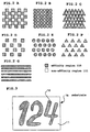
Embodiment 1 of the present invention relates to a substrate structure suited to the formation of a specific pattern. Figure 1 shows the appearance of the substrate inEmbodiment 1. Figure 1A is a plan view, and Figure 1B is a cross section along the A-A line in Figure 1A. As shown in Figure 1A, the substrate 1a ofEmbodiment 1 has apattern formation region 10 disposed in a pattern within apattern non-formation region 11 on the pattern formation side of a base. Thepattern formation region 10 is the region in which a thin film is formed by causing a specific fluid to adhere. Thepattern non-formation region 11 is the region in which this thin film is not formed. Thepattern non-formation region 11 becomes a region in which the base surface itself is exposed if the base is formed from a material that exhibits no affinity to the fluid. - The
pattern formation region 10 consists ofaffinity regions 110 having an affinity to the fluid, disposed alternately withnon-affinity regions 111 not having an affinity to the fluid. The alternating disposition of theaffinity regions 110 andnon-affinity regions 111 allows the fluid to be bonded in suitable amounts. Alternatively, the entire pattern formation region may consist of just anaffinity region 110. - The
affinity regions 110 can be disposed in a pattern in which square regions are touching each other as in Figure 2A, or in a pattern in which square regions have a specific spacing between them as in Figure 2D. They can also be disposed in a pattern in which circular regions are touching each other as in Figure 2B, or in a pattern in which circular regions have a specific spacing between them as in Figure 2E. They can also be disposed in a pattern in which triangular regions are touching each other as in Figure 2C, or in a pattern in which triangular regions have a specific spacing between them as in Figure 2F. Another possible pattern consists of parallel lines as in Figure 2G. In addition to these, any other polyhedral shapes, irregular shapes, or the like can be utilized. - Whether or not affinity is exhibited here is determined by the properties of the fluid with which the pattern is to be formed. For instance, if the fluid is one that includes polar molecules, such as water, then the surface region having polar groups will exhibit an affinity, while the surface region not having polar groups will not exhibit an affinity. Conversely, if the fluid is one that does not include polar molecules, such as many organic media, then the surface region having polar groups will not exhibit an affinity, while the surface region not having polar groups will exhibit an affinity. Which fluid to use is determined by what kind of material will be used to form the thin film. In this embodiment, the
pattern non-formation region 11 is the material of the base so that it will not exhibit an affinity to the fluid. Thenon-affinity regions 111 of thepattern formation region 10 are portions where the surface of the base is exposed, just as with thepattern non-formation region 11. - Table 1 shows examples of the materials that can be used as the
pattern non-formation region 11 andnon-affinity regions 111, and materials that can be used as theaffinity regions 110 in this embodiment.Constituent element When the fluid contains polar molecules When the fluid does not contain polar molecules Pattern non-formation region 11Non-affinity regions 111Bakelite, polyester, polyethylene, Teflon, PMMA, polypropylene, vinyl chloride polyvinyl alcohol, polyacrylic acid, nylon, glass Affinity regions 110 sulfur compounds having OH groups, silane coupling agents having OH, COOH, NH2, or other such groups sulfur compounds having alkyl groups, organic compound films (such as paraffin) - The shape, disposition, size, and so forth of the
pattern formation region 10 can be set as desired according to the intended application. Thepattern formation region 10 shown in Figure 1A consists of squares disposed in a regular pattern. Naturally, in addition to square, the shape of the pattern formation region may also be another polyhedral shape, circular, or an irregular shape. Thepattern formation region 10 may also be formed into graphics, such as characters or symbols, as shown in Figure 3. This applies to when a thin film of the fluid is made to adhere in the shape of characters, symbols, and so on. The disposition of the pattern formation region need not be regular, and may instead be irregular. There are no particular restrictions on the size of the pattern formation region, and this region can be variously increased or decreased in size. - Figures 5 and 6 show how the droplets adhere to a conventional substrate. Figure 5A is a cross section of when a plurality of
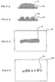
droplets 12 are discharged onto abase 100, and Figure 6A is a plan view thereof. If thedroplets 12 are continuously discharged onto a base on which a pattern formation region has not been formed as in this embodiment, then upon impact thedroplets 12 spread out as a result of surface tension, andadjacent droplets 12 join together as shown in Figure 5A. Since there is no boundary whatsoever for impeding this spreading of thedroplets 12, the profiles of the droplets spread out beyond the spreading that occurs upon impact, as shown in Figure 6A. If the fluid has a low solvent content, it will solidify while its profile is still spread out, making it difficult to form a fine pattern. If the solvent content is high, the solvent component in the droplets will be removed when the droplets are dried, and the droplets will shrink in the position where they landed. Since there are no restrictions on the adhesion position, thedroplets 12 that had initially linked together will split apart again and formislands 12b, as shown in Figures 5B and 6B. [A film] that splits up into theislands 12b will not work as a pattern. - The operation of the substrate 1a in the
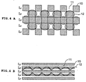
pattern formation region 10 of this embodiment will be described through reference to Figure 4. Figure 4A shows the form of the droplets on the substrate when droplets of fluid have adhered to the pattern in Figure 2A. Figure 4B shows the form of the droplets on the substrate when droplets of fluid have adhered to the pattern in Figure 2G. For both of the patterns in Figures 4A and 4B, we will assume that the droplets are bonded along a line L3 by an ink jet method. - As shown in Figure 4A, the
droplets 12 that land on the substrate spread out sufficiently in theaffinity regions 110. They are rejected, however, by thenon-affinity regions 111, and are drawn into theadjacent affinity regions 110 through surface tension. Therefore, after they are thus drawn by the action of their surface tension, thedroplets 12 only adhere to theaffinity regions 110, as shown in Figure 4A. Even though the direction in which the droplets are discharged from the head may vary somewhat, as long as thedroplets 12 land in a specific width from lines L2 to L4, they will always adhere in theaffinity regions 110 between lines L2 and L4. Since theaffinity regions 110 are separated from one another, or only touch at points, thedroplets 12 that are in asingle affinity region 110 will not infiltrateadjacent affinity regions 110 unless they land directly thereon. Sinceaffinity regions 110 bearingdroplets 12 are always touching or just slightly away next to [other]affinity regions 110 bearingdroplets 12, thedroplets 12 link together through surface tension. Therefore, thedroplets 12 link up along the path where they land, forming a contiguous pattern. Since theaffinity regions 110 bearingdroplets 12 are completely filled with droplets, adjacent droplets that have linked together do not separate when the droplets are dried. - As can be understood from the above, with the
pattern formation region 10 formed as in this embodiment, the fluid spreads out sufficiently in the region to which it adheres, but spreads no further. In other words, just the right amount of fluid adheres. As to the pattern layout of theaffinity regions 110, it is preferable for the individual patterns to be in point contact with one another. If the individual patterns are touching and linked completely, surface tension cannot be impeded at the affinity region boundaries, and there is the danger of uncontrolled infiltration by the droplets to adjoining affinity regions. Conversely, if the pattern spots are too far apart, this will impair the continuity of the droplets and lead to separation of the droplet pattern. - Meanwhile, with the linear pattern in Figure 4B, the
droplets 12 land along the line L3, andadjacent droplets 12 link up. With this linear pattern, as long as thedroplets 12 land between lines L2 and L4, they will be absorbed into the linking of the droplets centered on line L3, and the droplets will not spread out beyond the width from line L2 to line L4. Since line L3 is continuous, there will be no interruption in the droplet pattern as long as thedroplets 12 land so that they overlap. - When a pattern is formed using the
substrate 1[2] in this embodiment, any method that allows a fluid to adhere to the base surface can be applied. For instance, besides bonding by ink jet method, various coating methods such as spin coating, roll coating, die coating, and spray coating can also be applied. Because the substrate in this embodiment is structured such that a suitable amount of fluid will adhere, the fluid adheres evenly to thepattern formation region 10, but does not adhere to thepattern non-formation region 11, allowing the adhesion of the fluid to conform to the pattern. It is possible to form a thin film matching the pattern formation region by subjecting the adhering fluid to a heat treatment or the like to evaporate the solvent and produce a thin film. - As discussed above, this
Embodiment 1 allows a suitable amount of fluid to adhere in the pattern formation region, and the fluid does not adhere in the pattern non-formation region, so it is possible to form a thin film matching the pattern formation region. -
Embodiment 2 of the present invention relates to a method for manufacturing the substrate described inEmbodiment 1 above, in which paraffin or another such organic substance was used. - The manufacturing method of this embodiment will be described through reference to Figure 7. Figure 7 illustrates the substrate manufacturing process of the present invention in cross sections.
- Paraffin layer formation step (Figure 7A): The paraffin layer formation step is a step for forming a
paraffin layer 101 by coating the base 100 with paraffin. Thebase 100 is selected according to the fluid, that is, based on whether is has an affinity or does not have an affinity (hydrophobic, lipophilic) to the fluid. If the fluid contains no polar molecules, then ahydrophilic base 100 is used. If the fluid contains polar molecules, then a hydrophobic material is selected for thebase 100. Figure 7 shows the pattern formation when the fluid contains no polar molecules, in which case a hydrophilic material is used for thebase 100. For example, thebase 100 is made from poly-4-vinylpyrrolidone, polyethylene oxide, polyvinyl alcohol, cellulose, polyvinyl acetate, or the like. Roll coating, spin coating, spray coating, die coating, bar coating, or various other coating methods, or various printing methods, transfer methods, or the like can be applied for the formation of theparaffin layer 101. - Energy supply step (Figure 7B): The mask formation step[3] is a step in which the paraffin is evaporated by supplying energy to that part of the
paraffin layer 101 comprising thepattern non-formation region 11 and thenon-affinity regions 111 in thepattern formation region 10 when the fluid contains no polar molecules. Three types of energy are possible: optical, thermal, and optical and thermal [together], but the use of laser light is preferred for removing paraffin from a specific fine region. The paraffin may be evaporated by being irradiated with short-wavelength laser light, for example. - The aforementioned manufacturing step enables the
paraffin layer 101 to remain in theaffinity regions 110 of thepattern formation region 10. Adhesion of a non-polar molecule-containing fluid to the substrate will occur only in thepattern formation region 10. When a fluid to be adhered contains polar molecules, then supplying energy only to theaffinity regions 110 of thepattern formation region 10 will remove the paraffin. It is thereby possible to cause adhesion of polar molecule-containing fluids in theaffinity regions 110 only. - If the
base 100 is formed from a material that exhibits an affinity to the fluid, then it is manufactured so that the paraffin will remain in thepattern non-formation region 11 and in thenon-affinity regions 111 of thepattern formation region 10. If thebase 100 is formed from a material that exhibits no affinity to the fluid, then it is manufactured so that the paraffin will remain in theaffinity regions 110 of thepattern formation region 10. -
Embodiment 3 of the present invention relates to a method for manufacturing the substrate described inEmbodiment 1 above. In particular, this embodiment involves the use of a self-aggregating single-molecule film of a sulfur compound. - In this embodiment, a metal layer is provided to a base, and this product is immersed in a solution containing a sulfur compound to form a self-aggregating single-molecule film. The sulfur compound is made up of molecules having mercapto groups. This sulfur compound is dissolved in a 1 to 10 mM ethanol solution. A substrate on which a film of metal has been formed is immersed in this solution and allowed to stand for about an hour at room temperature, whereupon the sulfur compound spontaneously aggregates on the surface of the metal film. The atoms of metal and the sulfur atoms are covalently bonded, forming a single-molecule film of sulfur molecules two-dimensionally over the surface of the metal. The thickness of this film will vary with the molecular weight of the sulfur compound, but is about 10 to 50 angstroms. The self-aggregating single-molecule film can either be made to have or not to have an affinity to the fluid, as desired, by adjusting the composition of the sulfur compound.
- A thiol compound is favorable as the sulfur compound. "Thiol compound" as used here collectively refers to organic compounds having mercapto groups (R-SH, where R is an alkyl group or other hydrocarbon group, and -SH is a mercapto[4] group).
- Table 2 shows the typical compositions of thiol compounds having an affinity to a fluid, divided into a case when the fluid contains polar molecules and a case when no polar molecules are contained. n and m are natural numbers.
Fluid contains polar molecules Fluid does not contain polar molecules Composition of sulfur compound Sulfur compounds having OH groups or CO2H groups. HO2C(CH2)nSH, HO(CH2)nSH, etc. Linear alkanethiol expressed by CnH2n+2SH, fluorine compound expressed by CF3(CF2)m(CH2)nSH Composition of substrate Polyvinyl alcohol, polyacrylic acid, nylon, glass Bakelite, polyester, polyethylene, Teflon, PMMA, polypropylene, vinyl chloride - As can be seen from Table 2, the sulfur compound single-molecule film can be made to have an affinity to polar molecules or to have an affinity to non-polar molecules, as desired, by varying the composition. Figure 8 illustrates the substrate manufacturing process in this
Embodiment 3 in cross sections. - Metal layer formation step (Figure 8A): The metal layer formation step is a step in which a
metal layer 102 is formed on thebase 100. Thebase 100 is selected according to the fluid, that is, based on whether is has an affinity or does not have an affinity (hydrophobic, lipophilic) to the fluid. If the fluid contains no polar molecules, then ahydrophilic base 100 is used. If the fluid contains polar molecules, then a hydrophobic material is selected for thebase 100. Because of its chemical and physical stability, gold (Au) is preferred as themetal layer 102. In addition to gold, any metal that chemically adsorbs a sulfur compound may be used, such as silver (Ag), copper (Cu), indium (In), or gallium-arsenic (Ga-As). A known technique such as wet plating, vacuum vapor deposition, or vacuum sputtering can be used as the method for forming themetal layer 102. There are no particular restrictions on the type of method, however, as long as it is a film production method that allows a thin film of metal to be formed uniformly in a specific thickness. The role of the metal layer is to fix the sulfur compound layer, so the metal layer itself may be extremely thin. Accordingly, it may be formed in a thickness of about 500 to 2000 angstroms. - Depending on the
base 100, the adhesion between themetal layer 102 and the base 100 may be poor. In such a case, an interlayer is formed between the base 100 and themetal 102 in order to improve adhesion between the base and the metal layer. This interlayer is a material that increases the bonding strength between the base 100 and themetal layer 102, with favorable examples including nickel (Ni), chromium (Cr), tantalum (Ta),[5] and alloys of these (such as Ni-Cr). If an interlayer is provided, the bonding strength will be higher between the base 100 and themetal layer 102, and the sulfur compound layer will be more resistant to peeling as a result of mechanical abrasion. When an interlayer is formed under themetal layer 102, it is formed, for example, by applying chromium in a thickness of 100 to 300 angstroms by vacuum sputtering or ion plating. - Pattern formation step (Figure 8B): In the pattern formation step, metal is evaporated by applying energy to part of the
metal layer 102 formed on thebase 100. If the fluid contains polar molecules and thebase 100 is hydrophobic, or if the fluid does not contain polar molecules and thebase 100 is hydrophilic, then the energy is supplied to thepattern non-formation region 11 and to thenon-affinity regions 111 in thepattern formation region 10. If the fluid does not contain polar molecules and thebase 100 is hydrophobic, or if the fluid contains polar molecules and thebase 100 is hydrophilic, then the energy is only supplied to theaffinity regions 110 in thepattern formation region 10. Light is preferable as the energy, and laser light which can supply a high level of energy with a short wavelength is particularly favorable. A pick-up 200 is moved along pattern of the affinity regions or the non-affinity regions while emitting laser light. The metal that forms themetal layer 102 is evaporated from the region irradiated with the laser light, so the base 100 is exposed here. - Sulfur compound immersion step (Figure 8C): The sulfur compound immersion step is a step in which the substrate, including the metal layer from which part of the metal has been removed, is immersed in a solution of a sulfur compound to form a self-aggregating single-
molecule film 103. First, a solution is readied by dissolving a thiol compound of the composition used for the self-aggregating single-molecule film 103 in an organic solvent such as ethanol or isopropyl alcohol. For instance, if the fluid contains polar molecules and the self-aggregating single-molecule film 103 is to be made into theaffinity regions 110, then a hydrophilic sulfur compound solution is manufactured using a sulfur compound having OH or CO2H groups. If the fluid does not contain polar molecules and the self-aggregating single-molecule film 103 is to be made into theaffinity regions 110, then a hydrophilic sulfur compound solution is manufactured using a sulfur compound having alkyl groups. The base 100 that has been patterned with themetal layer 102 is then immersed in this solution. The immersion conditions comprise a sulfur compound concentration in the solution of 0.01 mM, a solution temperature of from normal temperature to about 50°C, and an immersion time of about 5 to 30 minutes. During the immersion treatment, the solution is agitated or circulated in order to form the sulfur compound layer more uniformly. - The sulfur molecules will aggregate on their own and form a single-molecule film if the metal surface is just kept clean, so this step does not require strict management of the conditions. Upon completion of the immersion, a single-molecule film of sulfur molecules having strong adhesion to just the surface of the metal is formed.
- Finally, the solution adhering to the base surface is washed away. Since the sulfur compound molecules adhering to portions other than the metal are not covalently bonded, they are easily washed away with a rinse of ethyl alcohol or the like.
- The above steps result in the manufacture of a
substrate 1 on which the self-aggregating single-molecule film 103 is formed in theaffinity regions 110 in thepattern formation region 10. - As discussed above, this
Embodiment 3 involves the use of a self-aggregating single-molecule film of a sulfur compound, allowing the manufacture of a substrate to which a liquid phase material can be stably bonded along a pattern. In particular, a self-aggregating single-molecule film of a sulfur compound is resistant to wear and has good physical and chemical resistance, making it suited to an industrial substrate. Appropriate selection of the sulfur compound allows the self-aggregating single-molecule film to be made either hydrophilic or hydrophobic according to the properties of the base. Furthermore, a fine pattern can be formed if laser light is used. - If the
base 100 is formed from a material that exhibits an affinity to the fluid, then the manufacture is such that a self-aggregating single-molecule film that exhibits no affinity remains in thepattern non-formation region 11 and in thenon-affinity regions 111 in thepattern formation region 10. If thebase 100 is formed from a material that exhibits no affinity to the fluid, then the manufacture is such that a self-aggregating single-molecule film that exhibits an affinity remains in theaffinity regions 110 in thepattern formation region 10. - Embodiment 4 of the present invention relates to a method for manufacturing the substrate of
Embodiment 1 by plasma treatment. - A plasma treatment involves the surface modification of a substrate by performing a high-voltage glow discharge under a specific atmospheric pressure. When an insulating substrate such as glass or plastic is subjected to a plasma treatment, a crosslinked layer and a large number of unreacted groups are generated on the substrate surface. When these are exposed to the air or an oxygen atmosphere, the unreacted groups are oxidized and form carbonyl groups or hydroxyl groups. Because these are polar groups, they have an affinity to a fluid containing polar molecules. On the other hand, most types of glass and plastic exhibit no affinity to a fluid containing polar molecules. Therefore, it is possible to produce affinity regions and non-affinity regions by selectively subjecting the pattern formation side of a substrate to a plasma treatment. This embodiment is based on this principle, and involves creating affinity regions and non-affinity regions by subjecting only part of the region to a plasma treatment by the use of a mask.
- The substrate manufacturing method of Embodiment 4 will now be described through reference to Figure 9.
- Mask formation step (Figure 9A): The mask formation step is a step in which a
mask 201 is applied over thebase 100. A material with which unreacted groups will appear upon irradiation with a plasma, [such as] a specific plastic, glass substrates whose surface has been coated with Teflon, and the like can be used as thebase 100. Themask 201 is formed in a pattern such that the mask will cover only those regions of the base 100 that are to be made hydrophobic. For instance, when a fluid containing polar molecules is used, the mask is provided so that thepattern non-formation region 11 and thenon-affinity regions 111 in thepattern formation region 10 will be exposed. The mask can be formed from a variety of materials, such as exposure masks, emulsion masks, and hard masks. When an exposure mask is used, it is formed from chromium, chromium oxide, silicon, silicon oxide, an oxidation film, or the like by vacuum vapor deposition, sputtering, CVD, or another such process. - Plasma irradiation step (Figure 9B): The plasma irradiation step is a step in which the
base 100 to which themask 201 has been applied is irradiated with aplasma 202. This plasma irradiation is carried out by glow discharge, in which a voltage of from several hundred to several thousand volts is applied using a neon transformer in argon gas of 10-1 to 100 Pa, for example. Other methods that can be applied include forming a discharge plasma by inductive coupling or capacity coupling using a discharge power source in the radio frequency band, and forming a discharge plasma by supplying microwave power to a discharge cell by waveguide. - This treatment generates ions, electrons, excited atoms or molecules, radicals, and so forth as active particles in the plasma, and changes the molecular structure of the surface of the
base 100. In other words, a crosslinked layer and a large number of unreacted groups appear at the portion irradiated with theplasm 202. - Surface modification step (Figure 9C): The surface modification step is a step in which the surface of the base 100 that has been plasma treated is modified through oxidation. The
base 100, on which unreacted groups and a crosslinked layer have appeared as a result of the above-mentioned plasma treatment, is exposed to the air or an oxygen atmosphere. The unreacted groups on the base 100 surface are oxidized intopolar groups 104, such as hydroxyl groups or carbonyl groups. Thesepolar groups 104 are hydrophilic and therefore readily wetted by water. Meanwhile, the region that was masked and not plasma treated is not hydrophilic, being unmodified plastic. - Therefore, the regions that were plasma treated become the
affinity regions 110, while the regions not plasma treated become thenon-affinity regions 111 or thepattern non-formation region 11. - Thus, with this Embodiment 4, the molecular structure of part of the region that makes up the base is changed by plasma treatment, which allows a film with no affinity to be changed into a film with an affinity, so the substrate of
Embodiment 1 can be provided without any new layer being formed. Because the composition is changed at the molecular level, this substrate is stable. - If the
base 100 is formed from a material that exhibits an affinity to the fluid, then the manufacture involves the plasma irradiation of thepattern non-formation region 11 and thenon-affinity regions 111 in thepattern formation region 10. If thebase 100 is formed from a material that exhibits no affinity to the fluid, then the manufacture involves the plasma irradiation of theaffinity regions 110 in thepattern formation region 10. - Embodiment 5 of the present invention relates to a method for manufacturing the substrate of
Embodiment 1 by ultraviolet irradiation. - Ultraviolet irradiation can be used as a means for modifying the surface of a resin, just as the above-mentioned plasma treatment can. If the substrate is formed from a resin such as polyester or polyethylene, or if it is covered with a thin film of these resins, because these resins are organic macromolecules with no polarity, the surface thereof inherently has no affinity to a fluid containing polar molecules, but has an affinity to a fluid not containing polar molecules. However, if this resin surface is irradiated with ultraviolet rays, the surface is activated just as with the plasma treatment, and OH groups or COOH groups appear. These groups are polar groups, so [the surface] ends up exhibiting an affinity to a fluid containing polar molecules. Affinity regions and non-affinity regions can be easily formed by using a mask to selectively irradiate with ultraviolet rays part of the pattern formation side of the substrate.
- The substrate manufacturing method of Embodiment 5 will now be described through reference to Figure 10.
- Mask formation step (Figure 10A): The mask formation step is a step in which a
mask 203 is applied over thebase 100. A material with which unreacted groups will appear upon irradiation with a plasma, and particularly a plastic such as polyester or polyethylene, is used as thebase 100. A substrate such as glass on whose surface is formed a thin film of one of these plastics can also be used. Themask 203 is formed in a pattern such that the mask will cover only those regions of the base 100 that are to be made hydrophobic. For instance, when a fluid containing polar molecules is used, the mask is provided so that theaffinity regions 110 in thepattern formation region 10 will be exposed and all other regions will be covered. The mask can be formed from a variety of materials, such as exposure masks, emulsion masks, and hard masks. When an exposure mask is used, it is formed from chromium, chromium oxide, silicon, silicon oxide, an oxidation film, or the like by vacuum vapor deposition, sputtering, CVD, or another such process. - Ultraviolet irradiation step (Figure 10B): The ultraviolet irradiation step is a step in which the
base 100 to which themask 203 has been applied is irradiated with ultraviolet rays. An ultraviolet lamp, for example, is used to perform this ultraviolet irradiation. This treatment excites the molecules and changes the covalent bond structure by applying energy in the form ofultraviolet rays 204 to the macromolecular surface of thebase 100. As a result, a large number of unreacted groups and a crosslinked layer appear in the exposed region of the base 100 irradiated with these ultraviolet rays 204. - Surface modification step (Figure 10C): The surface modification step is a step in which the surface of the base 100 that has undergone ultraviolet irradiation is modified through oxidation. When the
base 100, on which unreacted groups and a crosslinked layer have appeared as a result of the above-mentioned irradiation with the ultraviolet rays 204, is exposed to the air or an oxygen atmosphere, the unreacted groups on the base 100 surface are oxidized intopolar groups 105, such as hydroxyl groups or carbonyl groups. Thesepolar groups 104 have an affinity to a fluid such as water that contains polar molecules ([i.e., the groups are] hydrophilic) and therefore readily wetted by water. Meanwhile, the region that was masked and not exposed retains its properties as a plastic. In other words, it exhibits no affinity to a fluid containing polar molecules. Therefore, the regions that underwent ultraviolet irradiation become theaffinity regions 110, while the regions that did not undergo ultraviolet irradiation become thenon-affinity regions 111 or thepattern non-formation region 11. - Thus, with this Embodiment 5, the molecular structure of part of the region that makes up the base is changed by ultraviolet irradiation, which allows a film with no affinity to be changed into a film with an affinity, so the substrate of
Embodiment 1 can be provided without any new layer being formed. Because the composition is changed at the molecular level, this substrate is stable. - If the
base 100 is formed from a material that exhibits an affinity to the fluid, then the manufacture involves the ultraviolet irradiation of thepattern non-formation region 11 and thenon-affinity regions 111 in thepattern formation region 10. If thebase 100 is formed from a material that exhibits no affinity to the fluid, then the manufacture involves the ultraviolet irradiation of theaffinity regions 110 in thepattern formation region 10. - Embodiment 6 of the present invention relates to a method for manufacturing the substrate of
Embodiment 1 by photolithography. - The substrate manufacturing method of Embodiment 6 will now be described through reference to Figure 11. In the following description, we will assume that the base 100 exhibits no affinity to the fluid, and a layer that exhibits an affinity to the fluid is formed by photo-lithography in the
affinity regions 110 in thepattern formation region 10. However, if thebase 100 does exhibit an affinity to the fluid, then a layer that exhibits no affinity to the fluid is formed by photolithography in thepattern non-formation region 11 and in thenon-affinity regions 111 in thepattern formation region 10. - Affinity film formation step (Figure 11A): The affinity film formation step is a step in which a
thin film 106 is formed on the base surface from a material that exhibits an affinity to the fluid. Examples of thin film materials that exhibit an affinity to a fluid containing polar molecules include silane coupling agents having OH groups, COOH groups, NH2 groups, and so on. Spin coating, dipping, or another known thin film formation method can be employed as the method for forming this thin film. Thethin film 106 should be thick enough that it can be formed in a more or less uniform thickness by the above-mentioned manufacturing methods. - Exposure step (Figure 11B): The exposure step is a step in which the
thin film 106 is coated with aphotoresist 107 and masked according to the pattern formation, after which this is exposed and developed to leave behind thephotoresist 107. The photoresist can be a known material such as PMMA, PBS, or polyimide, and is determined by the relation between the etching method and thethin film material 106. After thephotoresist 107 has been applied by a coating method such as spinning, spraying, roll coating, or dipping, masking is performed in the same manner as described in Embodiment 4 or 5 above, and thephotoresist 107 is exposed. If the photoresist is a positive type, the mask covers theaffinity regions 110 in thepattern formation region 10. If the photoresist is a negative type, the mask covers thepattern non-formation region 11 and thenon-affinity regions 111 in thepattern formation region 10. The photoresist is exposed from above the mask by exposure to ordinary light or far ultraviolet rays. - Developing step (Figure 11C): The developing step is a step in which the
photoresist 107 is left behind in a pattern by developing the exposed photoresist. This developing is accomplished by causing a developer to adhere through spraying, dipping, or another such method. Next, a rinse liquid is made to adhere by the same method to remove any unnecessary photoresist. This treatment leaves behind thephotoresist 107 along the pattern on thethin film 106. - Etching step (Figure 11D): The etching step is a step in which the
thin film 106 and its remainingphotoresist 107 are etched to remove any unnecessarythin film 106. The etching liquid (in the case of wet etching) or etching gas (dry etching) is selected to be suited to the etching of thethin film 106, which is the material being etched. - The above step removes the
thin film 106 from everywhere except theaffinity regions 110 in thepattern formation region 10, and forms thepattern formation region 10 and thepattern non-formation region 11 on the base 100 surface. - As discussed above, with this Embodiment 6, it is also possible to manufacture the substrate of
Embodiment 1 by photolithography, which is commonly used as a thin film pattern formation method. - If the
base 100 is formed from a material that exhibits an affinity to the fluid, then the manufacture involves leaving a thin film that exhibits no affinity in thepattern non-formation region 11 and thenon-affinity regions 111 in thepattern formation region 10. If thebase 100 is formed from a material that exhibits no affinity to the fluid, then the manufacture involves leaving a thin film that exhibits an affinity in theaffinity regions 110 in thepattern formation region 10. - Embodiment 7 of the present invention relates to a method for manufacturing the substrate of
Embodiment 1 by application of a charge to the substrate. - Figure 12 illustrates the substrate manufacturing process in this Embodiment 7 in cross sections.
- Charge application step (Figure 12A): The charge application step is a step in which a charge is generated on the
base 100. A material that lends itself to charging is used for thebase 100. For example, if the material is a polymer, polyethylene terephthalate can be used. It is also possible to use PVK/Se, PVK-TNF, CFL/CTL, CTL/CGL, CTL (CGL), or the like, or an inorganic semiconductor based on selenium, Si:H, CdS, ZnO, or the like, which are used as photosensitive materials in laser printers. A charge application means such as a corona charger used in a laser printer is used in order to apply acharge 205 to the base 100 surface. The substrate surface is uniformly charged by bringing the corona charger or other charge application means into proximity therewith. In specific terms, a DC high voltage of 6 to 8 kV is applied to a tungsten wire with a diameter of 50 to 100 µm, and corona discharge is performed 8 to 10 mm away from the base surface. - Decharging step (Figure 12B): The decharging step is a step in which
energy 206 is selectively applied to the pattern formation side of the uniformly chargedbase 100 so as to partially release thecharge 205. Specifically, when optical energy or the like is supplied, optical carriers are produced and transport occurs in the exposed area, the surface charge is lost, and an electrostatic latent image is formed on the surface. Laser light is preferable as the energy supply source. This is because a latent image can be formed in a finer pattern. In addition, ultraviolet rays or other such optical energy may be added using a mask. When polyethylene terephthalate is used as the material for the base 100 as mentioned above, the decharged regions are thepattern non-formation region 11 and thenon-affinity regions 111 in thepattern formation region 10. - Bonding step (Figure 12C): The bonding step is a step in which electrostatic attraction is utilized to bond a
powder material 107[6] to the charged region that was not decharged. Thispowder material 107 is a material such as a toner for a laser printer, for instance, and a material that can be bonded by electrostatic force is used. The material used here becomes a surface that exhibits an affinity to a fluid containing polar molecules after fixing. This material can be steel, glass beads, iron powder, one of these that has been coated with a resin, a mixture of a magnetic material and a resin, or the like. In specific terms, thepowder material 107, which has the opposite polarity from that of the charged region on thebase 100, adheres by electrostatic force to the region where thecharge 205 is present. - Fixing step (Figure 12D): The fixing step is a step in which the
powder material 107 adhering to the base 100 surface is fixed. Once thepowder material 107 adheres to the charged region of thebase 100 due to the above-mentioned electrostatic force, heat is applied to the base 100 to melt thepowder material 107 and fix it to thebase 100. As a result, theaffinity regions 110 are formed by the fixing of the powder material in thepattern formation region 10. - As discussed above, with this Embodiment 7, the substrate of
Embodiment 1 comprising affinity regions and non-affinity regions can be manufactured by charging a substrate and fixing a powder material. - If the
base 100 is formed from a material that exhibits an affinity to the fluid, then the manufacture involves leaving a thin film of a powder material that exhibits no affinity in thepattern non-formation region 11 and thenon-affinity regions 111 in thepattern formation region 10. If thebase 100 is formed from a material that exhibits no affinity to the fluid, then the manufacture involves leaving a thin film of a powder material that exhibits an affinity in theaffinity regions 110 in thepattern formation region 10. - Embodiment 8 of the present invention relates to a manufacturing method in which a film is formed directly on a base by using a printing technique.
- Figure 13 illustrates the substrate manufacturing process in this Embodiment 8 in cross sections. Figure 13 serves to illustrate the manufacturing method when offset printing, which is a type of lithography, is utilized, for example.
- Printing step (Figure 13A): The printing step is a step in which a film having an affinity to the fluid, or a thin film with no affinity, is formed by a specific printing method. The printing apparatus must be one with which a hard substance such as a substrate can be printed. The difference from conventional printing is the use of a material that forms an affinity region or non-affinity region of the present invention instead of ink. If the 100 exhibits no affinity to a fluid containing polar molecules, the
material 108 is bonded by this printing apparatus to just theaffinity regions 110 in thepattern formation region 10. If the 100 exhibits an affinity to a fluid containing polar molecules, thematerial 108 is bonded by this printing apparatus to thepattern non-formation region 11 and to thenon-affinity regions 111 in thepattern formation region 10. In the figure, only thetransfer roll 207 is depicted out of the entire offset printing apparatus. Thethin film material 108 is transferred from thetransfer roll 207 to the pattern formation side of thebase 100. The printing method is not limited to offset printing, and can instead be direct printing or another lithographic method, or relief printing, intaglio printing, screen printing, a method that makes use of static electricity or magnetism, or the like. Specifically, any printing method with which a thin film material can be bonded instead of ink to a base by a known printing method can be applied. - Fixing step (Figure 13B): Once the thin film material has been transferred to the
base 100, a heat treatment or other known technique is applied in order to stabilize thethin film material 108. This step allows the manufacture of a substrate on which a thin film is formed only in theaffinity regions 110 in thepattern formation region 10. - As discussed above, with this Embodiment 8, the substrate of
Embodiment 1 can be manufactured by utilizing a known printing method to bond a thin film material. - If the
base 100 is formed from a material that exhibits an affinity to the fluid, then it is printed with a thin film exhibiting no affinity in thepattern non-formation region 11 and in thenon-affinity regions 111 in thepattern formation region 10. If thebase 100 is formed from a material that exhibits no affinity to the fluid, then it is printed with a thin film exhibiting an affinity in theaffinity regions 110 in thepattern formation region 10. - The present invention is not limited to the above embodiments, and many other variations are also possible.
- For instance, the disposition of the affinity region and the pattern shapes in which the base is formed shown in
Embodiment 1 are merely examples, and can be variously modified. Both a spotted pattern and a linear pattern can be variously modified in terms of the size, shape, and layout thereof. This is because these elements are determined according to the properties of the fluid. - Also, the method for manufacturing a substrate is not limited to those given in
Embodiments 2 to 8 above, and various permutations thereof are possible, as long as [the substrate] is divided into a pattern formation region and a pattern non-formation region. - With the present invention, a region having an affinity to a fluid and a region not having an affinity to a fluid are regularly disposed on a substrate, which makes it possible to provide a substrate with which a suitable amount of fluid can adhere to a pattern formation region of a specific surface area.
- Also, the present invention comprises a step for regularly disposing a region having an affinity to a fluid and a region not having an affinity on a substrate, which makes it possible to provide a method for manufacturing a substrate with which a suitable amount of fluid can adhere to a pattern formation region of a specific surface area.
- Therefore, a fine pattern that could not be formed in the past unless numerous steps were entailed using expensive equipment in a factory or the like can be manufactured easily and inexpensively.
Claims (18)
- A substrate for forming a specific pattern, being a substrate for forming a patterned thin film by causing a specific fluid to adhere,comprising a pattern formation region patterned in a specific shape for forming the thin film, andsaid pattern formation region being constituted by the disposition according to specific rules of an affinity region having an affinity to said fluid within a non-affinity region not having an affinity to said fluid.
- The substrate for forming a specific pattern defined in Claim 1, wherein a plurality of said pattern formation regions are disposed by specific rules.
- The substrate for forming a specific pattern defined in Claim 1, wherein said pattern formation region is formed in a specific graphic shape.
- A method for manufacturing a substrate for forming a patterned thin film by causing a specific fluid to adhere, comprising the steps of:forming a paraffin layer by applying a paraffin coating to a base that exhibits an affinity to the fluid; andremoving said paraffin layer by supplying energy to an affinity region having an affinity to said fluid such that said affinity region is disposed according to specific rules within a non-affinity region not having an affinity to said fluid in a pattern formation region in which said patterned film is formed.
- A method for manufacturing a substrate for forming a patterned thin film by causing a specific fluid to adhere, comprising the steps of:forming a paraffin layer by applying a paraffin coating to a base that exhibits no affinity to the fluid;removing said paraffin layer by supplying energy to a non-affinity region not having an affinity to said fluid such that an affinity region having an affinity to said fluid is disposed according to specific rules within said non-affinity region in a pattern formation region in which said patterned film is formed; andremoving said paraffin layer by supplying energy to a pattern non-formation region in which a patterned thin film is not formed.
- A method for manufacturing a substrate for forming a patterned thin film by causing a specific fluid to adhere, comprising the steps of:forming a metal layer from a specific metal on a base that exhibits an affinity to the fluid;removing said metal layer by supplying energy to an affinity region having an affinity to said fluid such that said affinity region is disposed according to specific rules within a non-affinity region not having an affinity to said fluid in a pattern formation region in which said patterned film is formed; andimmersing said base from which the metal has been selectively removed in a mixed liquid containing a sulfur compound.
- A method for manufacturing a substrate for forming a patterned thin film by causing a specific fluid to adhere, comprising the steps of:forming a metal layer from a specific metal on a base that exhibits no affinity to the fluid;removing said metal layer by supplying energy to the region other than the pattern formation region in which said patterned film is formed;removing said metal layer by supplying energy to a non-affinity region not having an affinity to said fluid such that an affinity region having an affinity to said fluid is disposed according to specific rules within said non-affinity region in said pattern formation region; andimmersing said base from which the metal has been selectively removed an a mixed liquid containing a sulfur compound.
- The method for manufacturing a substrate defined in either Claim 6 or 7, wherein said sulfur compound has the opposite property from that of the surface of said base in regard to affinity to said fluid.
- A method for manufacturing a substrate for forming a patterned thin film by causing a specific fluid to adhere, comprising the steps of:masking a base that exhibits no affinity to the fluid with a mesh mask that covers the region other than a pattern formation region in which said patterned thin film is formed and also covers a non-affinity region not having an affinity to said fluid such that an affinity region having an affinity to said fluid is disposed according to specific rules within said non-affinity region in said pattern formation region;plasma-working said base covered with the mesh mask; andperforming a modification treatment on the base surface that has been excited by said plasma working.
- A method for manufacturing a substrate for forming a patterned thin film by causing a specific fluid to adhere, comprising the steps of:masking a base that exhibits an affinity to the fluid with a mesh mask that covers an affinity region having an affinity to said fluid such that said affinity region is disposed according to specific rules within a non-affinity region not having an affinity to said fluid in a pattern formation region in which said patterned film is formed;plasma-working said base covered with the mesh mask; andperforming a modification treatment on the base surface that has been excited by said plasma working.
- A method for manufacturing a substrate for forming a patterned thin film by causing a specific fluid to adhere, comprising the steps of:masking a base that exhibits no affinity to the fluid with a mesh mask that covers the region other than a pattern formation region in which said patterned thin film is formed and also covers a non-affinity region not having an affinity to said fluid such that an affinity region having an affinity to said fluid is disposed according to specific rules within said non-affinity region in said pattern formation region; andperforming a modification treatment on said mesh-masked base by irradiating it with ultraviolet rays.
- A method for manufacturing a substrate for forming a patterned thin film by causing a specific fluid to adhere, comprising the steps of:masking a base that exhibits an affinity to the fluid with a mesh mask that covers an affinity region having an affinity to said fluid such that said affinity region is disposed according to specific rules within a non-affinity region not having an affinity to said fluid in a pattern formation region in which said patterned film is formed; andperforming a modification treatment on said mesh-masked base by irradiating it with ultraviolet rays.
- A method for manufacturing a substrate for forming a patterned thin film by causing a specific fluid to adhere, comprising the steps of:forming a thin film from a thin film material having an affinity to said fluid on a base furnished with a surface not having an affinity to the fluid;providing a photoresist such that an affinity region having an affinity to said fluid is disposed according to specific rules within a non-affinity region not having an affinity to said fluid in a pattern formation region in which said patterned film is formed; andetching the base on which said photoresist has been formed and etching the region other than the region where said photoresist is provided.
- A method for manufacturing a substrate for forming a patterned thin film by causing a specific fluid to adhere, comprising the steps of:forming a thin film from a thin film material not having an affinity to said fluid on a base furnished with a surface having an affinity to the fluid;providing a photoresist that covers the region other than a pattern formation region for forming said patterned thin film and also covers a non-affinity region not having an affinity to said fluid such that an affinity region having an affinity to said fluid is disposed according to specific rules within said non-affinity region in said pattern formation region; andetching the base on which said photoresist has been formed and etching the region other than the region where said photoresist is provided.
- A method for manufacturing a substrate for forming a patterned thin film by causing a specific fluid to adhere, comprising the steps of:applying a charge to the entire surface of a base that exhibits no affinity to the fluid;dissipating the charge by applying energy to the region other than a pattern formation region in which said patterned thin film is formed;dissipating the charge of a non-affinity region not having an affinity to said fluid such that an affinity region having an affinity to said fluid is disposed according to specific rules within said non-affinity region in said pattern formation region; andbonding a specific substance to the affinity region where the charge was not dissipated.
- A method for manufacturing a substrate for forming a patterned thin film by causing a specific fluid to adhere, comprising the steps of:applying a charge to the entire surface of a base that exhibits an affinity to the fluid;dissipating the charge of an affinity region having an affinity to said fluid such that said affinity region is disposed according to specific rules within a non-affinity region not having an affinity to said fluid in a pattern formation region in which said patterned thin film is formed; andbonding a specific substance to the affinity region where the charge was not dissipated.
- A method for manufacturing a substrate for forming a patterned thin film by causing a specific fluid to adhere, comprising the step of:printing an affinity film in an affinity region having an affinity to said fluid such that said affinity region is disposed according to specific rules within a non-affinity region not having an affinity to said fluid in a pattern formation region in which said patterned thin film is formed on a base that exhibits no affinity to the fluid.
- A method for manufacturing a substrate for forming a patterned thin film by causing a specific fluid to adhere, comprising the step of:printing a non-affinity film in the region other than a pattern formation region in which said patterned thin film is formed and in a disposed[7] affinity region having an affinity to said fluid such that said affinity region is disposed according to specific rules within a non-affinity region not having an affinity to said fluid in said pattern formation region on a base that exhibits an affinity to the fluid.
Applications Claiming Priority (3)
| Application Number | Priority Date | Filing Date | Title |
|---|---|---|---|
| JP13244698 | 1998-05-14 | ||
| JP13244698A JP3606047B2 (en) | 1998-05-14 | 1998-05-14 | Substrate manufacturing method |
| PCT/JP1999/002524 WO1999059386A1 (en) | 1998-05-14 | 1999-05-14 | Substrate for formation of special pattern, and method of manufacture of substrate |
Publications (3)
| Publication Number | Publication Date |
|---|---|
| EP1011298A1 true EP1011298A1 (en) | 2000-06-21 |
| EP1011298A4 EP1011298A4 (en) | 2003-08-27 |
| EP1011298B1 EP1011298B1 (en) | 2008-08-27 |
Family
ID=15081561
Family Applications (1)
| Application Number | Title | Priority Date | Filing Date |
|---|---|---|---|
| EP99919593A Expired - Lifetime EP1011298B1 (en) | 1998-05-14 | 1999-05-14 | Substrate for formation of special pattern, and method of manufacture of substrate |
Country Status (7)
| Country | Link |
|---|---|
| US (2) | US6733868B1 (en) |
| EP (1) | EP1011298B1 (en) |
| JP (1) | JP3606047B2 (en) |
| KR (1) | KR100597015B1 (en) |
| CN (2) | CN1247054C (en) |
| DE (1) | DE69939420D1 (en) |
| WO (1) | WO1999059386A1 (en) |
Cited By (9)
| Publication number | Priority date | Publication date | Assignee | Title |
|---|---|---|---|---|
| WO2004106077A1 (en) * | 2003-05-29 | 2004-12-09 | 3M Innovative Properties Company | Method for modifying the surface of substrate |
| EP1357772A3 (en) * | 2002-04-22 | 2005-01-19 | Seiko Epson Corporation | Manufacturing method for conductive layer wiring, layered structure member, electro-optic device, and electronic apparatus |
| WO2005014184A1 (en) * | 2003-07-18 | 2005-02-17 | Eastman Kodak Company | Method of pattern coating |
| FR2872911A1 (en) * | 2004-07-07 | 2006-01-13 | Commissariat Energie Atomique | METHOD FOR LOCATING A CHEMICAL OR BIOLOGICAL SPECIES ON A SUBSTRATE, MICROSYSTEM ANALYSIS AND BIOPUCE |
| WO2006046009A1 (en) * | 2004-10-29 | 2006-05-04 | Eastman Kodak Company | Method of multilayered patterned coating |
| WO2007003720A1 (en) * | 2005-07-01 | 2007-01-11 | Commissariat A L'energie Atomique | Low wetting hysteresis hydrophobic surface coating, method for depositing same, microcomponent and use |
| WO2006072066A3 (en) * | 2004-12-30 | 2007-09-07 | Du Pont | Organic electronic devices and methods |
| WO2007133419A2 (en) * | 2006-05-02 | 2007-11-22 | Boston Scientific Scimed, Inc. | Partially coated workpieces and method and system for making the same |
| EP2799154A1 (en) * | 2013-05-03 | 2014-11-05 | Nederlandse Organisatie voor toegepast -natuurwetenschappelijk onderzoek TNO | Slot-die coating method, apparatus, and substrate |
Families Citing this family (24)
| Publication number | Priority date | Publication date | Assignee | Title |
|---|---|---|---|---|
| JP3606047B2 (en) * | 1998-05-14 | 2005-01-05 | セイコーエプソン株式会社 | Substrate manufacturing method |
| JP2002340989A (en) * | 2001-05-15 | 2002-11-27 | Semiconductor Energy Lab Co Ltd | Measuring method, inspection method and inspection apparatus |
| US6973710B2 (en) * | 2001-08-03 | 2005-12-13 | Seiko Epson Corporation | Method and apparatus for making devices |
| JP4039035B2 (en) | 2001-10-31 | 2008-01-30 | セイコーエプソン株式会社 | Line pattern forming method, line pattern, electro-optical device, electronic device, non-contact card medium |
| US20030108725A1 (en) * | 2001-12-10 | 2003-06-12 | Matthew Hamilton | Visual images produced by surface patterning |
| GB0207350D0 (en) * | 2002-03-28 | 2002-05-08 | Univ Sheffield | Surface |
| JP2004066138A (en) * | 2002-08-07 | 2004-03-04 | Fujimori Gijutsu Kenkyusho:Kk | Thin film formation method, pattern formation method, and pattern formation apparatus |
| GB0313569D0 (en) * | 2003-06-12 | 2003-07-16 | Plasso Technology Ltd | Method |
| KR100623227B1 (en) * | 2004-05-27 | 2006-09-19 | 학교법인 영남학원 | Electrical printed devices fabricating method by offset printing process |
| DE102004058209A1 (en) * | 2004-12-02 | 2006-06-08 | Printed Systems Gmbh | Method and device for producing structures from functional materials |
| JP4151652B2 (en) * | 2005-01-11 | 2008-09-17 | セイコーエプソン株式会社 | Identification code drawing method |
| JP4929115B2 (en) * | 2007-09-28 | 2012-05-09 | 本田技研工業株式会社 | Painted metal product for outboard motor and its manufacturing method |
| JP5206154B2 (en) * | 2008-06-27 | 2013-06-12 | 富士通株式会社 | Wiring board manufacturing method |
| US8173552B2 (en) * | 2009-08-04 | 2012-05-08 | Intel Corporation | Method of fabricating an identification mark utilizing a liquid film assisted by a laser |
| JP5402511B2 (en) * | 2009-10-19 | 2014-01-29 | セイコーエプソン株式会社 | Liquid crystal device, manufacturing method thereof, and electronic apparatus |
| JP5797883B2 (en) * | 2010-06-07 | 2015-10-21 | 住友電気工業株式会社 | PCB for printed wiring board |
| US8828484B2 (en) * | 2013-01-28 | 2014-09-09 | Taiwan Semiconductor Manufacturing Co., Ltd. | Self-alignment due to wettability difference of an interface |
| CN103213940B (en) * | 2013-03-15 | 2016-04-06 | 北京工业大学 | One makes material have two kinds of infiltrating methods of difference based on micro-nano-scale |
| USD765327S1 (en) * | 2013-06-27 | 2016-08-30 | The Procter & Gamble Company | Pad |
| US9305807B2 (en) * | 2014-02-27 | 2016-04-05 | Palo Alto Research Center Incorporated | Fabrication method for microelectronic components and microchip inks used in electrostatic assembly |
| WO2016194968A1 (en) * | 2015-06-02 | 2016-12-08 | 株式会社村田製作所 | Metal layer formation method |
| DE102015224992A1 (en) * | 2015-12-11 | 2017-06-14 | Robert Bosch Gmbh | Method of microstructured application of a liquid or paste to a surface |
| WO2019177120A1 (en) * | 2018-03-16 | 2019-09-19 | Agc株式会社 | Film-coated base |
| JP2021181158A (en) * | 2018-08-20 | 2021-11-25 | Agc株式会社 | Method for producing base material with film |
Citations (12)
| Publication number | Priority date | Publication date | Assignee | Title |
|---|---|---|---|---|
| FR701903A (en) * | 1929-03-31 | 1931-03-25 | Process for applying colored designs to leather, etc. | |
| GB850934A (en) * | 1956-11-05 | 1960-10-12 | Keller Eberhard | Improvements in or relating to processes and apparatus for the production of coloured self-adhesive plates from aluminium foil |
| DE3535696A1 (en) * | 1985-10-05 | 1987-04-09 | Klaus Kalwar | Process and apparatus for the partial coating of a plastic part |
| US4729310A (en) * | 1982-08-09 | 1988-03-08 | Milliken Research Corporation | Printing method |
| US4833486A (en) * | 1987-07-08 | 1989-05-23 | Dataproducts Corporation | Ink jet image transfer lithographic |
| US4879176A (en) * | 1987-03-16 | 1989-11-07 | Minnesota Mining And Manufacturing Company | Surface modification of semicrystalline polymers |
| EP0351793A2 (en) * | 1988-07-19 | 1990-01-24 | VALEO VISION S.p.A. | A process for the production of a headlamp reflector made of a synthetic thermoplastic polymer, and a headlamp reflector made by such a process |
| WO1995021030A1 (en) * | 1994-02-07 | 1995-08-10 | The Government Of The United States Of America, Represented By The Secretary Of The Navy | Efficient chemistry for selective modification and metallization of substrates |
| EP0769331A1 (en) * | 1995-10-06 | 1997-04-23 | Ford Motor Company | Method for identifying and protecting an activated plastic surface |
| EP0794015A1 (en) * | 1996-03-04 | 1997-09-10 | Motorola, Inc. | Apparatus and method for patterning a surface |
| WO1997038802A1 (en) * | 1996-04-12 | 1997-10-23 | The Texas A & M University System | Polymeric self-assembled mono- and multilayers and their use in photolithography |
| WO1998040169A1 (en) * | 1997-03-14 | 1998-09-17 | The University Of Houston | Methods for making fluorinated surface modifying agents, methods of using same and products made using same |
Family Cites Families (25)
| Publication number | Priority date | Publication date | Assignee | Title |
|---|---|---|---|---|
| US3673961A (en) | 1960-04-27 | 1972-07-04 | Eastman Kodak Co | Xerothermographic process |
| NL139829B (en) * | 1964-03-21 | 1973-09-17 | Philips Nv | PROCESS FOR THE MANUFACTURE OF PHOTOSENSITIVE MATERIAL, THEREFORE MANUFACTURED PHOTOSENSITIVE MATERIAL AND OBJECT FROM THIS. |
| US3554125A (en) | 1967-04-26 | 1971-01-12 | Xerox Corp | Method of making a lithographic master and method of printing therewith |
| JPS5143769A (en) | 1974-10-14 | 1976-04-14 | Asahi Chemical Ind | 11 beeta dd arabinofuranoshirushitoshinjudotaino seizoho |
| JPS574116B2 (en) * | 1975-02-07 | 1982-01-25 | ||
| JPS51106638A (en) * | 1975-03-17 | 1976-09-21 | Hitachi Ltd | Zetsuentaihyomenno fukatsuseikaho |
| JPS5240886A (en) | 1975-09-29 | 1977-03-30 | Toshiba Corp | Cutting method by ultra hard alloy of titanium nitride and cutting too ls |
| JPS51108638A (en) * | 1976-02-23 | 1976-09-27 | Toyo Terumii Kk | MUDENKAIBUBUNMETSUKIHO |
| JPS51115658A (en) | 1976-03-16 | 1976-10-12 | Matsushita Electric Ind Co Ltd | Flux coating device |
| JPS58222592A (en) * | 1982-03-15 | 1983-12-24 | イ−ストマン・コダツク・カンパニ− | Method of forming conductive pattern |
| JPS5975205A (en) | 1982-10-25 | 1984-04-27 | Seiko Epson Corp | Manufacture of color filter |
| US5059513A (en) | 1983-11-01 | 1991-10-22 | Hoechst Celanese Corporation | Photochemical image process of positive photoresist element with maleimide copolymer |
| JPS6333895A (en) * | 1986-07-29 | 1988-02-13 | キヤノン株式会社 | Manufacture of electric circuit |
| JPS63270474A (en) * | 1986-12-10 | 1988-11-08 | Minoru Tsuda | Catalytic ink |
| JPS645095A (en) * | 1987-06-26 | 1989-01-10 | Tdk Corp | Formation of conductive pattern |
| US4836105A (en) | 1987-12-10 | 1989-06-06 | International Business Machines Corporation | Direct negative and offset master production using thermal liftoff |
| US5145758A (en) | 1988-07-29 | 1992-09-08 | Man Roland Druckmaschinen Ag | Method of producing a printing image carrier |
| US5272979A (en) | 1989-03-29 | 1993-12-28 | Presstek, Inc. | Plasma-jet imaging apparatus and method |
| US5254429A (en) | 1990-12-14 | 1993-10-19 | Anocoil | Photopolymerizable coating composition and lithographic printing plate produced therefrom |
| JPH05202483A (en) * | 1991-04-25 | 1993-08-10 | Shipley Co Inc | Method and composition for electroless metallization |
| US5468597A (en) | 1993-08-25 | 1995-11-21 | Shipley Company, L.L.C. | Selective metallization process |
| JPH07245467A (en) * | 1994-03-07 | 1995-09-19 | Ibiden Co Ltd | Manufacture of printed wiring board |
| JPH1115000A (en) * | 1997-06-26 | 1999-01-22 | Seiko Epson Corp | Liquid crystal display device and its manufacture |
| JP3960561B2 (en) * | 1998-01-28 | 2007-08-15 | セイコーエプソン株式会社 | Liquid ejection structure, ink jet recording head and printer |
| JP3606047B2 (en) * | 1998-05-14 | 2005-01-05 | セイコーエプソン株式会社 | Substrate manufacturing method |
-
1998
- 1998-05-14 JP JP13244698A patent/JP3606047B2/en not_active Expired - Fee Related
-
1999
- 1999-05-14 KR KR1020007000370A patent/KR100597015B1/en not_active IP Right Cessation
- 1999-05-14 CN CNB99801138XA patent/CN1247054C/en not_active Expired - Fee Related
- 1999-05-14 WO PCT/JP1999/002524 patent/WO1999059386A1/en active IP Right Grant
- 1999-05-14 CN CNA2005100676068A patent/CN1697598A/en active Pending
- 1999-05-14 DE DE69939420T patent/DE69939420D1/en not_active Expired - Lifetime
- 1999-05-14 EP EP99919593A patent/EP1011298B1/en not_active Expired - Lifetime
-
2000
- 2000-08-02 US US09/630,444 patent/US6733868B1/en not_active Expired - Lifetime
-
2004
- 2004-03-10 US US10/796,056 patent/US20040169004A1/en not_active Abandoned
Patent Citations (12)
| Publication number | Priority date | Publication date | Assignee | Title |
|---|---|---|---|---|
| FR701903A (en) * | 1929-03-31 | 1931-03-25 | Process for applying colored designs to leather, etc. | |
| GB850934A (en) * | 1956-11-05 | 1960-10-12 | Keller Eberhard | Improvements in or relating to processes and apparatus for the production of coloured self-adhesive plates from aluminium foil |
| US4729310A (en) * | 1982-08-09 | 1988-03-08 | Milliken Research Corporation | Printing method |
| DE3535696A1 (en) * | 1985-10-05 | 1987-04-09 | Klaus Kalwar | Process and apparatus for the partial coating of a plastic part |
| US4879176A (en) * | 1987-03-16 | 1989-11-07 | Minnesota Mining And Manufacturing Company | Surface modification of semicrystalline polymers |
| US4833486A (en) * | 1987-07-08 | 1989-05-23 | Dataproducts Corporation | Ink jet image transfer lithographic |
| EP0351793A2 (en) * | 1988-07-19 | 1990-01-24 | VALEO VISION S.p.A. | A process for the production of a headlamp reflector made of a synthetic thermoplastic polymer, and a headlamp reflector made by such a process |
| WO1995021030A1 (en) * | 1994-02-07 | 1995-08-10 | The Government Of The United States Of America, Represented By The Secretary Of The Navy | Efficient chemistry for selective modification and metallization of substrates |
| EP0769331A1 (en) * | 1995-10-06 | 1997-04-23 | Ford Motor Company | Method for identifying and protecting an activated plastic surface |
| EP0794015A1 (en) * | 1996-03-04 | 1997-09-10 | Motorola, Inc. | Apparatus and method for patterning a surface |
| WO1997038802A1 (en) * | 1996-04-12 | 1997-10-23 | The Texas A & M University System | Polymeric self-assembled mono- and multilayers and their use in photolithography |
| WO1998040169A1 (en) * | 1997-03-14 | 1998-09-17 | The University Of Houston | Methods for making fluorinated surface modifying agents, methods of using same and products made using same |
Non-Patent Citations (4)
| Title |
|---|
| "FABRICATION OF GOLD NANOSTRUCTURES BY LITHOGRAPHY WITH SELF-ASSEMBLED MONOLAYERS" IBM TECHNICAL DISCLOSURE BULLETIN, IBM CORP. NEW YORK, US, vol. 39, no. 12, 1 December 1996 (1996-12-01), pages 235-238, XP000686075 ISSN: 0018-8689 * |
| DRAKE J: "Chemical Technology in printing and imaging systems" CHEMICAL TECHNOLOGY IN PRINTING AND IMAGING SYSTEMS. YORK, OCT. 6 - 7, 1992, PROCEEDINGS OF THE SYMPOSIUM ON CHEMICAL TECHNOLOGY IN PRINTING AND IMAGING SYSTEMS, CAMBRIDGE, RSC, GB, 1992, pages 33-35,58-59, XP002189010 * |
| GILLEN G ET AL: "PATTERNING OF SELF-ASSEMBLED ALKANETHIOL MONOLAYERS ON SILVER BY MICROFOCUS ION AND ELECTRON BEAM BOMBARDMENT" APPLIED PHYSICS LETTERS, AMERICAN INSTITUTE OF PHYSICS. NEW YORK, US, vol. 65, no. 5, 1 August 1994 (1994-08-01), pages 534-536, XP000464868 ISSN: 0003-6951 * |
| See also references of WO9959386A1 * |
Cited By (18)
| Publication number | Priority date | Publication date | Assignee | Title |
|---|---|---|---|---|
| EP1357772A3 (en) * | 2002-04-22 | 2005-01-19 | Seiko Epson Corporation | Manufacturing method for conductive layer wiring, layered structure member, electro-optic device, and electronic apparatus |
| WO2004106077A1 (en) * | 2003-05-29 | 2004-12-09 | 3M Innovative Properties Company | Method for modifying the surface of substrate |
| US6969166B2 (en) | 2003-05-29 | 2005-11-29 | 3M Innovative Properties Company | Method for modifying the surface of a substrate |
| WO2005014184A1 (en) * | 2003-07-18 | 2005-02-17 | Eastman Kodak Company | Method of pattern coating |
| FR2872911A1 (en) * | 2004-07-07 | 2006-01-13 | Commissariat Energie Atomique | METHOD FOR LOCATING A CHEMICAL OR BIOLOGICAL SPECIES ON A SUBSTRATE, MICROSYSTEM ANALYSIS AND BIOPUCE |
| WO2006005887A1 (en) * | 2004-07-07 | 2006-01-19 | Commissariat A L'energie Atomique | Method for localizing a chemical or biological species on a substrate, analyzing microsystem and biochip |
| WO2006046009A1 (en) * | 2004-10-29 | 2006-05-04 | Eastman Kodak Company | Method of multilayered patterned coating |
| WO2006072066A3 (en) * | 2004-12-30 | 2007-09-07 | Du Pont | Organic electronic devices and methods |
| US8481104B2 (en) | 2004-12-30 | 2013-07-09 | E I Du Pont De Nemours And Company | Method of forming organic electronic devices |
| KR101290012B1 (en) * | 2004-12-30 | 2013-07-30 | 이 아이 듀폰 디 네모아 앤드 캄파니 | Organic electronic devices and methods |
| WO2007003720A1 (en) * | 2005-07-01 | 2007-01-11 | Commissariat A L'energie Atomique | Low wetting hysteresis hydrophobic surface coating, method for depositing same, microcomponent and use |
| US7989056B2 (en) | 2005-07-01 | 2011-08-02 | Commissariat A L'energie Atomique | Hydrophobic surface coating with low wetting hysteresis, method for depositing same, microcomponent and use |
| WO2007133419A2 (en) * | 2006-05-02 | 2007-11-22 | Boston Scientific Scimed, Inc. | Partially coated workpieces and method and system for making the same |
| WO2007133419A3 (en) * | 2006-05-02 | 2008-07-24 | Boston Scient Scimed Inc | Partially coated workpieces and method and system for making the same |
| EP2799154A1 (en) * | 2013-05-03 | 2014-11-05 | Nederlandse Organisatie voor toegepast -natuurwetenschappelijk onderzoek TNO | Slot-die coating method, apparatus, and substrate |
| WO2014178716A1 (en) * | 2013-05-03 | 2014-11-06 | Nederlandse Organisatie Voor Toegepast-Natuurwetenschappelijk Onderzoek Tno | Slot-die coating method, apparatus, and substrate |
| CN105358260A (en) * | 2013-05-03 | 2016-02-24 | 荷兰应用自然科学研究组织Tno | Slot-die coating method, apparatus, and substrate |
| US9640760B2 (en) | 2013-05-03 | 2017-05-02 | Nederlandse Organisatie Voor Toegepast—Natuurwetenschappelijk Onderzoek Tno | Slot-die coating method, apparatus, and substrate |
Also Published As
| Publication number | Publication date |
|---|---|
| CN1274516A (en) | 2000-11-22 |
| EP1011298A4 (en) | 2003-08-27 |
| EP1011298B1 (en) | 2008-08-27 |
| CN1697598A (en) | 2005-11-16 |
| JP3606047B2 (en) | 2005-01-05 |
| JPH11330666A (en) | 1999-11-30 |
| KR20010021806A (en) | 2001-03-15 |
| CN1247054C (en) | 2006-03-22 |
| DE69939420D1 (en) | 2008-10-09 |
| US6733868B1 (en) | 2004-05-11 |
| US20040169004A1 (en) | 2004-09-02 |
| WO1999059386A1 (en) | 1999-11-18 |
| KR100597015B1 (en) | 2006-07-06 |
Similar Documents
| Publication | Publication Date | Title |
|---|---|---|
| EP1011298A1 (en) | Substrate for formation of special pattern, and method of manufacture of substrate | |
| JP3539179B2 (en) | A substrate, a method of manufacturing a substrate, an integrated circuit, and a method of manufacturing an integrated circuit. | |
| KR100707236B1 (en) | Metal pattern and process for producing the same | |
| US20080047930A1 (en) | Method to form a pattern of functional material on a substrate | |
| US20040035605A1 (en) | Methods and apparatus for manufacturing electronic and electromechanical elements and devices by thin-film deposition and imaging | |
| KR101105991B1 (en) | Deposition and patterning process | |
| KR940004732A (en) | Pattern formation method and thin film formation method used for pattern formation | |
| WO2001077753A1 (en) | Photoimageable, aqueous acid soluble polyimide polymers | |
| WO2008118340A2 (en) | Method to form a pattern of functional material on a substrate including the treatment of a surface of a stamp | |
| WO2008118341A1 (en) | Method to form a pattern of functional material on a substrate using a stamp having a surface modifying material | |
| WO2009097301A1 (en) | Method for forming a thin layer of particulate on a substrate | |
| WO2008124130A1 (en) | Method to form a pattern of functional material on a substrate using a mask material | |
| KR20090015634A (en) | A method for forming metal pattern by using surface characteristics and metal patten formed thereby | |
| JP3921917B2 (en) | Manufacturing method of fine structure | |
| EP1831764A2 (en) | Nanofabrication based on sam growth | |
| JP2006021491A (en) | Laminated structure, optics using laminated structure, display element, arithmetic element and method for manufacturing these elements | |
| JP4100378B2 (en) | Pattern forming substrate and manufacturing method thereof | |
| JP4507893B2 (en) | Wiring board | |
| WO2002059985A1 (en) | Method of producing a track on a substrate | |
| JP3956930B2 (en) | substrate | |
| JP2009056685A (en) | Plate used for reverse offset printing, letterpress printing and intaglio printing, plate forming method, and printed matter forming method | |
| WO2017018103A1 (en) | Method for manufacturing wiring board and wiring board | |
| JPH11237793A (en) | Image forming mesh member and its production as well as image forming device using this mesh member | |
| JP2009135123A (en) | Pattern forming apparatus | |
| JPH09314891A (en) | Manufacture of electrode body |
Legal Events
| Date | Code | Title | Description |
|---|---|---|---|
| PUAI | Public reference made under article 153(3) epc to a published international application that has entered the european phase |
Free format text: ORIGINAL CODE: 0009012 |
|
| 17P | Request for examination filed |
Effective date: 20000114 |
|
| AK | Designated contracting states |
Kind code of ref document: A1 Designated state(s): DE FR GB NL |
|
| RIC1 | Information provided on ipc code assigned before grant |
Free format text: 7H 05K 1/02 A, 7H 05K 3/18 B, 7B 05D 1/32 B |
|
| A4 | Supplementary search report drawn up and despatched |
Effective date: 20030715 |
|
| RIC1 | Information provided on ipc code assigned before grant |
Ipc: 7B 05D 1/18 B Ipc: 7B 05D 3/06 B Ipc: 7B 05D 3/14 B Ipc: 7B 05D 1/32 B Ipc: 7H 05K 3/18 B Ipc: 7H 05K 1/02 A |
|
| 17Q | First examination report despatched |
Effective date: 20051230 |
|
| GRAP | Despatch of communication of intention to grant a patent |
Free format text: ORIGINAL CODE: EPIDOSNIGR1 |
|
| GRAS | Grant fee paid |
Free format text: ORIGINAL CODE: EPIDOSNIGR3 |
|
| GRAA | (expected) grant |
Free format text: ORIGINAL CODE: 0009210 |
|
| AK | Designated contracting states |
Kind code of ref document: B1 Designated state(s): DE FR GB NL |
|
| REG | Reference to a national code |
Ref country code: GB Ref legal event code: FG4D |
|
| REF | Corresponds to: |
Ref document number: 69939420 Country of ref document: DE Date of ref document: 20081009 Kind code of ref document: P |
|
| PG25 | Lapsed in a contracting state [announced via postgrant information from national office to epo] |
Ref country code: NL Free format text: LAPSE BECAUSE OF FAILURE TO SUBMIT A TRANSLATION OF THE DESCRIPTION OR TO PAY THE FEE WITHIN THE PRESCRIBED TIME-LIMIT Effective date: 20080827 |
|
| PLBE | No opposition filed within time limit |
Free format text: ORIGINAL CODE: 0009261 |
|
| STAA | Information on the status of an ep patent application or granted ep patent |
Free format text: STATUS: NO OPPOSITION FILED WITHIN TIME LIMIT |
|
| 26N | No opposition filed |
Effective date: 20090528 |
|
| REG | Reference to a national code |
Ref country code: FR Ref legal event code: PLFP Year of fee payment: 17 |
|
| PGFP | Annual fee paid to national office [announced via postgrant information from national office to epo] |
Ref country code: GB Payment date: 20150513 Year of fee payment: 17 Ref country code: DE Payment date: 20150506 Year of fee payment: 17 |
|
| PGFP | Annual fee paid to national office [announced via postgrant information from national office to epo] |
Ref country code: FR Payment date: 20150508 Year of fee payment: 17 |
|
| REG | Reference to a national code |
Ref country code: DE Ref legal event code: R119 Ref document number: 69939420 Country of ref document: DE |
|
| GBPC | Gb: european patent ceased through non-payment of renewal fee |
Effective date: 20160514 |
|
| REG | Reference to a national code |
Ref country code: FR Ref legal event code: ST Effective date: 20170131 |
|
| PG25 | Lapsed in a contracting state [announced via postgrant information from national office to epo] |
Ref country code: FR Free format text: LAPSE BECAUSE OF NON-PAYMENT OF DUE FEES Effective date: 20160531 Ref country code: DE Free format text: LAPSE BECAUSE OF NON-PAYMENT OF DUE FEES Effective date: 20161201 |
|
| PG25 | Lapsed in a contracting state [announced via postgrant information from national office to epo] |
Ref country code: GB Free format text: LAPSE BECAUSE OF NON-PAYMENT OF DUE FEES Effective date: 20160514 |