EP1008169B1 - Producing microstructures or nanostructures on a support - Google Patents
Producing microstructures or nanostructures on a support Download PDFInfo
- Publication number
- EP1008169B1 EP1008169B1 EP98939717A EP98939717A EP1008169B1 EP 1008169 B1 EP1008169 B1 EP 1008169B1 EP 98939717 A EP98939717 A EP 98939717A EP 98939717 A EP98939717 A EP 98939717A EP 1008169 B1 EP1008169 B1 EP 1008169B1
- Authority
- EP
- European Patent Office
- Prior art keywords
- crystalline
- lattice
- wafer
- defects
- wafers
- Prior art date
- Legal status (The legal status is an assumption and is not a legal conclusion. Google has not performed a legal analysis and makes no representation as to the accuracy of the status listed.)
- Expired - Lifetime
Links
Images
Classifications
-
- H—ELECTRICITY
- H01—ELECTRIC ELEMENTS
- H01L—SEMICONDUCTOR DEVICES NOT COVERED BY CLASS H10
- H01L21/00—Processes or apparatus adapted for the manufacture or treatment of semiconductor or solid state devices or of parts thereof
- H01L21/02—Manufacture or treatment of semiconductor devices or of parts thereof
- H01L21/04—Manufacture or treatment of semiconductor devices or of parts thereof the devices having at least one potential-jump barrier or surface barrier, e.g. PN junction, depletion layer or carrier concentration layer
- H01L21/18—Manufacture or treatment of semiconductor devices or of parts thereof the devices having at least one potential-jump barrier or surface barrier, e.g. PN junction, depletion layer or carrier concentration layer the devices having semiconductor bodies comprising elements of Group IV of the Periodic System or AIIIBV compounds with or without impurities, e.g. doping materials
- H01L21/30—Treatment of semiconductor bodies using processes or apparatus not provided for in groups H01L21/20 - H01L21/26
- H01L21/302—Treatment of semiconductor bodies using processes or apparatus not provided for in groups H01L21/20 - H01L21/26 to change their surface-physical characteristics or shape, e.g. etching, polishing, cutting
- H01L21/306—Chemical or electrical treatment, e.g. electrolytic etching
-
- B—PERFORMING OPERATIONS; TRANSPORTING
- B82—NANOTECHNOLOGY
- B82Y—SPECIFIC USES OR APPLICATIONS OF NANOSTRUCTURES; MEASUREMENT OR ANALYSIS OF NANOSTRUCTURES; MANUFACTURE OR TREATMENT OF NANOSTRUCTURES
- B82Y10/00—Nanotechnology for information processing, storage or transmission, e.g. quantum computing or single electron logic
-
- B—PERFORMING OPERATIONS; TRANSPORTING
- B82—NANOTECHNOLOGY
- B82Y—SPECIFIC USES OR APPLICATIONS OF NANOSTRUCTURES; MEASUREMENT OR ANALYSIS OF NANOSTRUCTURES; MANUFACTURE OR TREATMENT OF NANOSTRUCTURES
- B82Y30/00—Nanotechnology for materials or surface science, e.g. nanocomposites
-
- H—ELECTRICITY
- H01—ELECTRIC ELEMENTS
- H01L—SEMICONDUCTOR DEVICES NOT COVERED BY CLASS H10
- H01L21/00—Processes or apparatus adapted for the manufacture or treatment of semiconductor or solid state devices or of parts thereof
- H01L21/02—Manufacture or treatment of semiconductor devices or of parts thereof
- H01L21/02002—Preparing wafers
-
- H—ELECTRICITY
- H01—ELECTRIC ELEMENTS
- H01L—SEMICONDUCTOR DEVICES NOT COVERED BY CLASS H10
- H01L21/00—Processes or apparatus adapted for the manufacture or treatment of semiconductor or solid state devices or of parts thereof
- H01L21/02—Manufacture or treatment of semiconductor devices or of parts thereof
- H01L21/04—Manufacture or treatment of semiconductor devices or of parts thereof the devices having at least one potential-jump barrier or surface barrier, e.g. PN junction, depletion layer or carrier concentration layer
- H01L21/18—Manufacture or treatment of semiconductor devices or of parts thereof the devices having at least one potential-jump barrier or surface barrier, e.g. PN junction, depletion layer or carrier concentration layer the devices having semiconductor bodies comprising elements of Group IV of the Periodic System or AIIIBV compounds with or without impurities, e.g. doping materials
- H01L21/185—Joining of semiconductor bodies for junction formation
Definitions
- the present invention relates to the production of microstructures or nanostructures on a support.
- microstructures and the nanostructures for still smaller dimensions, are in the form of a network of microvolumes of material obtained on the surface of a support.
- microvolume means, for example, volumes of parallelepiped shape, preferably smaller than one micrometer.
- microstructures in semiconductor material and in particular in silicon, AsGa, III-V compounds and SiC.
- conducting materials such as metals, and dielectric materials such as SiO 2 .
- micro- or nanostructures are intended for the production of electronic, optical or optoelectronic devices.
- this type of structure allows the realization of a quantum dot array (called “quantum dots” in the English terminology), or electronic devices called mono-electron or Coulomb blocking (“Coulomb blockade”) or else light emitting devices.
- microstructures When we want to make microstructures, we use the techniques today in the field of microelectronics. In particular, the principles of lithography combined with dry or wet etching, ion implantation, deposition and heat treatment operations are used. For example, if one wants to make a square network of parallelepiped microvolumes monocrystalline silicon, each microvolume having 1 micron side to 0.2 microns thick, microvolumes being spaced from each other by 0.5 microns, can start from a SSI (Silicon On Insulator) wafer having a 0.2 micron thick monocrystalline silicon layer.
- SSI Silicon On Insulator
- a layer of photosensitive resin is applied to the silicon layer of the wafer and is insulated by means of an Electron Beam Pattern Generator ("Electron Beam Pattern Generator") so as to inscribe in the resin a matrix of rows and columns 0.5 ⁇ m wide representing the spaces between the microvolumes.
- the development of the resin releases the exposed parts, exposing the silicon layer corresponding to the array of rows and columns.
- the wafer is then subjected to a plasma etching treatment selectively attacking the silicon with respect to the resin. The etching process ends when the underlying silica layer is reached.
- an array of microvolumes each having 1 ⁇ m ⁇ 1 ⁇ m ⁇ 0.2 ⁇ m in size and spaced 0.5 ⁇ m apart is obtained. If necessary, the spaces between microvolumes can then be filled by a dielectric layer such as SiO 2 , or by using a thermal oxidation process or a CVD type deposit.
- microstructures with microvolumes of much smaller dimensions for example a few tens of nanometers
- condensation nuclei randomly distributed on the surface can be obtained.
- microstructures are multiple and depend on the particular properties of each. These properties are related to a size effect on the electronic states of carriers in these materials, surface effects, interface effects, the existence or not of intergranular phases, etc.
- a particular application is the production of light emitters, in particular from materials such as silicon which, in the solid monocrystalline state, are not emitters (see the article by T. KOMOKA already cited).
- Another application is the realization of electronic devices based on the quantum confinement of electronic carriers in microvolumes of the structure or Coulomb blocking effects. This application is described in the article " Modeling the Multiplicity of Conductance Structures in Clusters of Silicon Quantum Dots by DW BOERINGER and R. TSU, published in Mat. Res, Soc Symp, Proc Vol 358, pp. 569-574, 1995. , Materials Research Society.
- the present invention has been designed to allow the production of microstructures that may include microvolumes of dimensions significantly smaller than microvolumes currently achievable, for example a few tens of nm, economically and over large areas.
- these microstructures are organized according to a predetermined plan instead of being randomly distributed.
- the invention proposes a process for producing micro- or nanostructures, which applies to crystalline materials, whether they are semiconductors, conductors or dielectrics.
- the disagree parameter can be constituted by a given angle of offset in rotation of the crystal lattices presented by said faces.
- the network of defects obtained, called “twist” is a network of dislocations to character screws.
- the disagreement parameter can also be constituted by a difference in crystal lattice parameter between the crystalline materials of the faces of the wafers put in contact with the resulting defect network is called "misfit".
- the detuning parameter can also be constituted by a determined angle according to which the face of at least one of the platelets is offset with respect to the single crystallographic plane of direction corresponding to this face.
- the disoriented crystalline faces (one or both) with respect to a simple crystallographic plane are called vicinal.
- the fault network is called "miscut”.
- mismatch parameters are possible, for example by gluing two different materials and offset in rotation. Several networks are then formed.
- the contacting may preferably be hydrophobic type, that is to say, direct bonding of the faces of said wafers. It may be of the hydrophilic type, that is to say involving a thin intermediate layer, for example an oxide layer formed naturally on one face of a wafer or on the faces of the wafers.
- the method also comprises at least one heat treatment step intended either to complete the formation of the crystal defect network and / or the constraint network if the contacting is insufficient to complete it, or to complete it completely.
- this treatment may be able to reinforce the interatomic bonds between the faces of the platelets put in contact.
- This heat treatment can be performed before or after the thinning step.
- the thinning step may be carried out using a technique chosen from grinding, mechanical abrasion or chemical abrasion.
- the thinning step may also be carried out by cleaving one of the platelets which, before the contacting step has been subjected, through its contacting face, to an ion implantation step intended to create, at a determined depth and corresponding to the desired thinning, a layer of microcavities capable of generating a cleavage plane during a subsequent heat treatment step.
- the ion implantation can be carried out by means of hydrogen ions.
- the thinning step it can be provided at least one heat treatment step simultaneously making it possible to complete or complete the formation of the lattice of crystalline defects and / or the network of stresses, to reinforce the interatomic bonds between the faces of the platelets contacted and generate the cleavage plane.
- the micro- or nanostructure after the thinning step, it may be provided a step of selectively treating the lattice of crystalline defects and / or the stress network with respect to said crystalline zone .
- This selective treatment step may consist of conductive crystalline defects and / or the network of stresses so that said crystalline zone forms crystalline pads electrically connected to each other. In this case, it is possible to carry out a phosphorus diffusion which diffuses preferentially at the level of the crystalline defects.
- the selective treatment step may also consist of electrical insulation so that said crystalline zone forms crystalline pads electrically insulated from each other.
- the chemical etching may be preceded by a crystalline defects decoration phase and / or the stress network by precipitation of metal impurities or dopants.
- the network of defects produced by the techniques indicated above extends a small thickness on either side of the bonding surface of the two wafers.
- the stresses induced by these defects extend on each side of the interface, in the wafers, over distances of the order of magnitude of the dislocation period.
- the thinning of one of the platelets can be done by stopping the operation at a distance from the interface which is of the same order of magnitude.
- the surface stress field is nonuniform and is in the image of the underlying defect network.
- the selective treatment step can then consist in depositing, for example by epitaxy, a crystalline crystal detuned crystalline material with the crystalline material revealed by the thinning step, this deposited crystalline material forming an ordered set of islands in correspondence with the lattice of underlying crystal defects.
- the electrical isolation of the selective treatment may be of the type where electrical conduction can take place by a physical effect such as the tunnel effect or the Fowler-Nordheim effect.
- the selective treatment step can also consist in treating the crystalline defects and / or the network of stresses so that said crystalline zone forms crystalline pads connected to each other by semiconductor zones or having a potential barrier.
- the subject of the invention is also a micro- or nanostructure on a support, characterized in that it is obtained according to the method described above from platelets whose faces to be in contact are made of semiconductor materials. At least one of these faces to be contacted may be SiC or III-V semiconductor material such as AsGa or GaAlAs.
- the subject of the invention is also a micro-or nanostructure on a support, characterized in that it is obtained according to the method described above, one of the wafers consisting of a silicon-on-insulator wafer, Another wafer being made of silicon and constituting the thinned wafer, the method making it possible to obtain a micro- or nanostructure consisting of microvolumes of silicon on an insulating layer.
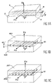
- FIGS. 1A, 1B and 1C illustrate three variants of implementation of the method according to the present invention.
- X 1 , X 2 and X 3 represent the crystallographic axes.
- the parameter that adjusts the defect density (or the average distance between defects) is the angle of rotation ⁇ existing between the crystal lattices presented by the faces contacted platelets 1 and 2.
- the parameter which regulates the density of defects (or the average distance between defects) is the angle of rotation ⁇ existing between the crystallographic planes of the plates 101 and 102 contacted.
- the parameter that adjusts the defect density (or the average distance between defects) is the mesh mismatch f 1 between the two crystalline materials of the platelets 201 and 202 contacted.
- one of the platelets can be prepared with a vicinal side shifted in the ⁇ 100> direction of 0.8 ° and glued on a non-vicinal silicon wafer (100).
- the densities of nanostructures obtained are then 2.7 ⁇ 10 15 / m 2 .
- a silicon wafer (100) is adhered to a second wafer having a SiGe layer on its surface. Since the mismatch f 1 is 2.1%, a 20 nm corner dislocation interface grating is formed. After thinning the wafer comprising the SiGe layer to approximately 10 nm, and after revelation by one of the described techniques, a density of nanostructures of the same order of magnitude as above is obtained. The bonding of a germanium wafer would produce a double clash and thus a density of nanostructures four times higher.
- Faces other than faces (100) may be used.
- the faces (111) produce at their interface hexagonal or triangular networks of dislocations.
- Faces (110) produce rectangular gratings.
- the Figure 1A shows two platelets 1 and 2 in silicon of crystallographic plane (1,0,0) when they come into contact and having plane faces, respectively 3 and 4, facing each other.
- the flat faces 3 and 4 received a surface treatment to make them hydrophobic. This will ensure an intimate and adherent contact of the faces 3 and 4.
- This surface treatment comprises a chemical cleaning step ending for example by a hydrofluoric acid etching step.
- the faces 3 and 4 are brought into contact with adhesion by molecular adhesion, for example at ambient temperature, ensuring that the crystal lattices presented by the two faces are offset relative to one another by an angle ⁇ determined, for example 0.6 °.
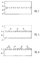
- the assembly constituted by these two inserts is then subjected to a heat treatment at a temperature of about 950 ° C for about 30 minutes. During this heat treatment, stronger and more numerous interatomic bonds are established between the two platelets. Due to the torsion angle existing between the two crystal lattices, an array of crystal defects, for example a dislocation lattice, is established in the vicinity of the interface between the two platelets, in a thin layer (a few tens to a few hundred nm) centered on the interface. This is schematically represented on the figure 2 where the reference 5 designates this interface, the crystalline defects (or dislocations) being represented under the reference 6.
- the spacing between two adjacent dislocations is a function of the ⁇ rotation angle of the crystal lattices of the two platelets.
- a surface treatment can then be implemented to differentiate, more specifically, the crystalline defects of the surrounding crystalline zone 8.
- Lateral dielectric isolation of microvolumes 9 can be performed.
- the oxide layer deposited on the microstructure 7 may be leveled, as shown in FIG. figure 4 , to keep only a deposit of insulation 11 between the microvolumes 9. In this case, we obtain a network of insulating material replacing the dislocation network.
- dislocation network conductive can also be carried out to make the dislocation network conductive, insulative, or even semiconductor depending on the intended application. This makes it possible to make the microvolumes or pads crystalline, either electrically connected to one another by conductive bonds, or electrically isolated, or connected by semiconductor zones or having a potential barrier. With regard to the electrical insulation, insulations such as electrical conduction through the insulating parts can also take place by tunnel effect for example, or by the Fowler-Nordheim effect or by any other physical effect. To make the dislocation network conductive, it is possible to carry out a phosphorus diffusion which diffuses preferentially at the level of the dislocations.
- Another possibility of carrying out the thinning step consists in applying the process described in the document FR-A-2,681,472 in order to obtain a cleavage of the wafer concerned.
- protons are implanted in this wafer to obtain a layer of microcavities at the desired depth of the face to be brought into contact. This face undergoes the cleaning and bonding treatment. The heat treatment is then applied. It allows to generate simultaneously the creation of dislocations and cleavage according to the layer of microcavities.
- One of the wafers may be an SSI (Silicon-On-Insulator) wafer called SOI ("Silicon on Insulator") in the English terminology and the other wafer may be a solid substrate. of silicon.
- SOI Silicon-On-Insulator
- the method according to the invention then provides a network of microvolumes of silicon on an insulating layer.
- the two platelets of crystalline material may be of a different nature, for example a silicon wafer and a gallium arsenide wafer, or a silicon wafer and a germanium wafer.
- platelets are not necessarily homogeneous. It suffices simply that the faces to be brought into contact are of crystalline material, the rest of the wafers may have other structures.
- the micro- or nanostructure can still be obtained from a network of constraints.
- This network of constraints can be revealed by various techniques.
- the constraint network can be revealed by deposition, by an epitaxial process (MOCVD, MBE, liquid phase epitaxy ...), on the thinned plate of a crystalline mesh detuned crystalline material.
- MOCVD epitaxial process
- MBE liquid phase epitaxy
- the preferential nucleation sites provided by the zones in compression (respectively in tension) will be favorable for the smaller (respectively larger) mesh deposits than the thinned plate.
- An ordered set of islands of size corresponding to the underlying network will thus be formed.
- This deposit can be illustrated from the variant of the process illustrated by the figure 1C .
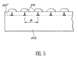
- An assembly has been prepared according to this variant, as described above, from an orientation silicon wafer (100) and a wafer comprising the SiGe layer. After thinning, we obtain the assembly represented at figure 5 where reference 202 designates the silicon wafer and the reference 201 'remains of the SiGe layer.
- a deposit of pure germanium is carried out under Stranski-Krastanov growth conditions. Nano-sized germanium islands 210 are nucleated vertically above the nodes of the dislocation network, in the stress-stress zones.
Abstract
Description
La présente invention concerne la réalisation de microstructures ou de nanostructures sur un support.The present invention relates to the production of microstructures or nanostructures on a support.
Les microstructures, et les nanostructures pour des dimensions encore inférieures, se présentent sous la forme d'un réseau de microvolumes de matériau obtenus à la surface d'un support. Par microvolume, on entend par exemple des volumes de forme parallélépipédique, de dimensions préférentiellement inférieures au micromètre.The microstructures, and the nanostructures for still smaller dimensions, are in the form of a network of microvolumes of material obtained on the surface of a support. By microvolume means, for example, volumes of parallelepiped shape, preferably smaller than one micrometer.
Généralement, on s'intéresse à des microstructures en matériau semiconducteur et en particulier en silicium, en AsGa, en composés III-V et en SiC. Cependant, on s'intéresse également aux matériaux conducteurs, tels que les métaux, et aux matériaux diélectriques tels que SiO2.Generally, one is interested in microstructures in semiconductor material and in particular in silicon, AsGa, III-V compounds and SiC. However, there is also interest in conducting materials, such as metals, and dielectric materials such as SiO 2 .
Ces micro- ou nanostructures sont destinées à la réalisation de dispositifs électroniques, optiques ou optoélectroniques. En particulier, ce type de structures permet la réalisation d'un réseau de boîtes quantiques (appelées "quantum dots" dans la terminologie anglo-saxonne), ou de dispositifs électroniques dits mono-électrons ou à blocage de Coulomb ("Coulomb blockade") ou encore de dispositifs émetteurs de lumière.These micro- or nanostructures are intended for the production of electronic, optical or optoelectronic devices. In particular, this type of structure allows the realization of a quantum dot array (called "quantum dots" in the English terminology), or electronic devices called mono-electron or Coulomb blocking ("Coulomb blockade") or else light emitting devices.
Lorsque l'on veut réaliser des microstructures, on utilise les techniques aujourd'hui classiques du domaine de la micro-électronique. En particulier, on utilise les principes de la lithographie combinée avec des opérations de gravure sèche ou humide, d'implantation ionique, de dépôts et de traitement thermique. Par exemple, si l'on veut réaliser un réseau carré de microvolumes parallélépipédiques en silicium monocristallin, chaque microvolume ayant 1 µm de côté pour 0,2 µm d'épaisseur, les microvolumes étant espacés les uns des autres de 0,5 µm, on peut partir d'une plaquette SSI (Silicium Sur Isolant) présentant une couche de silicium monocristallin de 0,2 µm d'épaisseur. On applique sur la couche de silicium de la plaquette une couche de résine photosensible que l'on insole grâce à une machine d'insolation à faisceau d'électrons ("Electron Beam Pattern Generator") de façon à inscrire dans la résine une matrice de lignes et de colonnes de largeur 0,5 µm représentant les espaces entre les microvolumes. Le développement de la résine dégage les parties exposées, mettant à nu la couche de silicium correspondant à la matrice de lignes et de colonnes. La plaquette est alors soumise à un traitement de gravure plasma attaquant sélectivement le silicium par rapport à la résine. Le procédé de gravure se termine quand la couche de silice sous-jacente est atteinte. Après enlèvement de la résine, on obtient un réseau de microvolumes ayant chacun 1 µm × 1 µm × 0,2 µm de dimensions et espacées de 0,5 µm. Si nécessaire, les espaces entre microvolumes peuvent être ensuite comblés par une couche diélectrique telle que SiO2, soit en utilisant un procédé d'oxydation thermique, soit un dépôt du type CVD.When we want to make microstructures, we use the techniques today in the field of microelectronics. In particular, the principles of lithography combined with dry or wet etching, ion implantation, deposition and heat treatment operations are used. For example, if one wants to make a square network of parallelepiped microvolumes monocrystalline silicon, each microvolume having 1 micron side to 0.2 microns thick, microvolumes being spaced from each other by 0.5 microns, can start from a SSI (Silicon On Insulator) wafer having a 0.2 micron thick monocrystalline silicon layer. A layer of photosensitive resin is applied to the silicon layer of the wafer and is insulated by means of an Electron Beam Pattern Generator ("Electron Beam Pattern Generator") so as to inscribe in the resin a matrix of rows and columns 0.5 μm wide representing the spaces between the microvolumes. The development of the resin releases the exposed parts, exposing the silicon layer corresponding to the array of rows and columns. The wafer is then subjected to a plasma etching treatment selectively attacking the silicon with respect to the resin. The etching process ends when the underlying silica layer is reached. After removal of the resin, an array of microvolumes each having 1 μm × 1 μm × 0.2 μm in size and spaced 0.5 μm apart is obtained. If necessary, the spaces between microvolumes can then be filled by a dielectric layer such as SiO 2 , or by using a thermal oxidation process or a CVD type deposit.
La réalisation d'un réseau de microvolumes peut aussi être obtenue en utilisant un procédé de lithographie par interférométrie ou holographie comme le divulgue l'article "
L'utilisation de ces techniques permet la réalisation de microstructures pour des dimensions de l'ordre du micromètre ou de quelques dixièmes de micromètre. Pour obtenir les meilleures résolutions en terme de lithographie, on utilise l'insolation par faisceau d'électrons ou un photorépéteur sur tranche fonctionnant avec une longueur d'onde de 248 nm ou 193 nm.The use of these techniques allows the production of microstructures for dimensions of the order of a micrometer or a few tenths of a micrometer. To obtain the best resolution in terms of lithography, electron beam irradiation or a wafer photorépéteur operating at a wavelength of 248 nm or 193 nm is used.
Pour réaliser des microstructures avec des microvolumes de dimensions bien inférieures (par exemple quelques dizaines de nanomètres), il n'existe pas de moyens connus dès lors que l'on souhaite obtenir, de façon économiquement acceptable et sur de grandes surfaces, des microstructures organisées selon un plan d'organisation prédéterminé.To make microstructures with microvolumes of much smaller dimensions (for example a few tens of nanometers), there are no known means when it is desired to obtain, economically acceptable and over large areas, organized microstructures. according to a predetermined organization plan.
On peut noter cependant que l'on peut réaliser des microvolumes d'un premier matériau à l'intérieur d'une matrice d'un deuxième matériau, par exemple en introduisant dans cette matrice, par implantation ionique, des atomes du premier matériau en une concentration telle et avec un traitement thermique tel que ces atomes se rassemblent en précipités à l'intérieur de la matrice. On peut ainsi obtenir des précipités de silicium dans une matrice de SiO2 de l'ordre de 10 nm. Une telle technique est décrite par exemple dans l'article "
De façon analogue, en réalisant un dépôt (par exemple, par évaporation) sur une surface, on peut obtenir des noyaux de condensation répartis au hasard sur la surface. L'article "
Les applications de ces microstructures sont multiples et dépendent des propriétés particulières de chacune. Ces propriétés sont liées à un effet de taille sur les états électroniques des porteurs dans ces matériaux, aux effets de surface, d'interface, à l'existence ou non de phases intergranulaires, etc. Une application particulière est la réalisation d'émetteurs de lumière, notamment à partir de matériaux tels que le silicium qui, à l'état monocristallin massif ne sont pas émetteurs (voir l'article de T. KOMOKA déjà cité). Une autre application est la réalisation de dispositifs électroniques basés sur le confinement quantique des porteurs électroniques dans les microvolumes de la structure ou à des effets de blocage de Coulomb. Cette application est décrite dans l'article "
Dans l'article de
La présente invention a été conçue afin de permettre la réalisation de micro-structures pouvant comporter des microvolumes de dimensions nettement inférieures aux microvolumes réalisables actuellement, par exemple quelques dizaines de nm, de façon économique et sur de grandes surfaces. En outre, ces microstructures sont organisées selon un plan prédéterminé au lieu d'être réparties au hasard.The present invention has been designed to allow the production of microstructures that may include microvolumes of dimensions significantly smaller than microvolumes currently achievable, for example a few tens of nm, economically and over large areas. In addition, these microstructures are organized according to a predetermined plan instead of being randomly distributed.
L'invention propose un procédé de réalisation, de micro- ou de nanostructures, qui s'applique à des matériaux cristallins, qu'ils soient semiconducteurs, conducteurs ou diélectriques.The invention proposes a process for producing micro- or nanostructures, which applies to crystalline materials, whether they are semiconductors, conductors or dielectrics.
L'invention a donc pour objet un procédé de réalisation de micro- ou de nanostructure sur un support, caractérisé en ce qu'il comporte les étapes suivantes :
- collage par mise en contact d'une face d'une première plaquette en matériau cristallin avec une face d'une deuxième plaquette en matériau cristallin, de façon que les réseaux cristallins présentés par lesdites faces présentent au moins un paramètre de désaccord apte à permettre la formation d'un réseau de défauts cristallins et/ou d'un réseau de contraintes au sein d'une zone cristalline s'étendant de part et d'autre de l'interface des deux plaquettes, au moins l'un desdits réseaux définissant la micro- ou la nanostructure,
- amincissement de l'une des deux plaquettes pour faire apparaître le réseau de défauts et/ou le réseau de contraintes sur un support constitué par l'autre plaquette et traitement sélectif du réseau de défauts cristallins et/ou du réseau de contraintes.
- bonding by contacting a face of a first wafer of crystalline material with a face of a second wafer of crystalline material, so that the crystal lattices presented by said faces have at least one detuning parameter capable of enabling the forming a network of crystalline defects and / or a network of stresses within a crystalline zone extending on either side of the interface of the two wafers, at least one of said networks defining the micro- or nanostructure,
- thinning of one of the two wafers to reveal the network of defects and / or the network of constraints on a support constituted by the other wafer and selective treatment of the lattice of crystalline defects and / or the network of constraints.
Le paramètre de désaccord peut être constitué par un angle déterminé de décalage en rotation des réseaux cristallins présentés par lesdites faces. Le réseau de défauts obtenu, dit de "twist" est un réseau de dislocations à caractère vis.The disagree parameter can be constituted by a given angle of offset in rotation of the crystal lattices presented by said faces. The network of defects obtained, called "twist" is a network of dislocations to character screws.
Le paramètre de désaccord peut aussi être constitué par une différence de paramètre de maille cristalline entre les matériaux cristallins des faces des plaquettes mises en contact le réseau de défauts obtenu est dit de "misfit".The disagreement parameter can also be constituted by a difference in crystal lattice parameter between the crystalline materials of the faces of the wafers put in contact with the resulting defect network is called "misfit".
Le paramètre de désaccord peut encore être constitué par un angle déterminé selon lequel la face d'au moins l'une des plaquettes est décalée par rapport au plan cristallographique simple de direction correspondant à cette face. Les faces cristallines désorientées (une seule ou les deux) par rapport à un plan cristallographique simple sont dites vicinales. Le réseau de défaut est dit de "miscut".The detuning parameter can also be constituted by a determined angle according to which the face of at least one of the platelets is offset with respect to the single crystallographic plane of direction corresponding to this face. The disoriented crystalline faces (one or both) with respect to a simple crystallographic plane are called vicinal. The fault network is called "miscut".
Toutes les combinaisons de paramètres de désaccord sont possibles, par exemple en collant deux matériaux différents et décalés en rotation. Plusieurs réseaux sont alors formés.All combinations of mismatch parameters are possible, for example by gluing two different materials and offset in rotation. Several networks are then formed.
La mise en contact peut être préférentiellement du type hydrophobe, c'est-à-dire à collage direct des faces desdites plaquettes. Elle peut être du type hydrophile, c'est-à-dire impliquant une fine couche intermédiaire, par exemple une couche d'oxyde formée naturellement sur une face d'une plaquette ou sur les faces des plaquettes.The contacting may preferably be hydrophobic type, that is to say, direct bonding of the faces of said wafers. It may be of the hydrophilic type, that is to say involving a thin intermediate layer, for example an oxide layer formed naturally on one face of a wafer or on the faces of the wafers.
Avantageusement, le procédé comporte en outre au moins une étape de traitement thermique destinée soit à compléter la formation du réseau de défauts cristallins et/ou du réseau de contraintes si la mise en contact est insuffisante pour l'achever, soit à l'achever complètement. De plus, ce traitement peut être apte à renforcer les liaisons interatomiques entre les faces des plaquettes mises en contact. Ce traitement thermique peut être réalisé avant ou après l'étape d'amincissement.Advantageously, the method also comprises at least one heat treatment step intended either to complete the formation of the crystal defect network and / or the constraint network if the contacting is insufficient to complete it, or to complete it completely. . In addition, this treatment may be able to reinforce the interatomic bonds between the faces of the platelets put in contact. This heat treatment can be performed before or after the thinning step.
L'étape d'amincissement peut être réalisée au moyen d'une technique choisie parmi la rectification, l'abrasion mécanique ou l'abrasion chimique.The thinning step may be carried out using a technique chosen from grinding, mechanical abrasion or chemical abrasion.
L'étape d'amincissement peut aussi être réalisée par clivage de l'une des plaquettes qui, avant l'étape de mise en contact a été soumise, au travers de sa face à mettre en contact, à une étape d'implantation ionique destinée à créer, à une profondeur déterminée et correspondant à l'amincissement désirée, une couche de microcavités susceptible de générer un plan de clivage lors d'une étape postérieure de traitement thermique. L'implantation ionique peut être réalisée au moyen d'ions hydrogène. Dans le cas où l'étape d'amincissement est ainsi réalisée, il peut être prévu au moins une étape de traitement thermique permettant simultanément de compléter ou d'achever la formation du réseau de défauts cristallins et/ou du réseau de contraintes, de renforcer les liaisons interatomiques entre les faces des plaquettes mises en contact et de générer le plan de clivage.The thinning step may also be carried out by cleaving one of the platelets which, before the contacting step has been subjected, through its contacting face, to an ion implantation step intended to create, at a determined depth and corresponding to the desired thinning, a layer of microcavities capable of generating a cleavage plane during a subsequent heat treatment step. The ion implantation can be carried out by means of hydrogen ions. In the case where the thinning step is thus performed, it can be provided at least one heat treatment step simultaneously making it possible to complete or complete the formation of the lattice of crystalline defects and / or the network of stresses, to reinforce the interatomic bonds between the faces of the platelets contacted and generate the cleavage plane.
En fonction des utilisations auxquelles la micro- ou la nanostructure est destinée, après l'étape d'amincissement, il peut être prévu une étape consistant à traiter sélectivement le réseau de défauts cristallins et/ou le réseau de contraintes par rapport à ladite zone cristalline. Ceci permet en particulier d'accentuer la différence de comportement physique/électrique ou optoélectronique des défauts cristallins par rapport à ladite zone cristalline ou, de façon plus générale, de délimiter des micro- ou nanovolumes dans ou au-dessus de la zone cristalline. Cette étape de traitement sélectif peut consister à rendre conducteurs les défauts cristallins et/ou le réseau de contraintes de manière que ladite zone cristalline forme des plots cristallins reliés électriquement entre eux. Dans ce cas, on peut procéder à une diffusion de phosphore qui diffuse préférentiellement au niveau des défauts cristallins. L'étape de traitement sélectif peut aussi consister en une isolation électrique afin que ladite zone cristalline forme des plots cristallins isolés électriquement entre eux. Dans ce cas, on peut procéder à une attaque chimique du réseau de défauts cristallins et/ou du réseau de contraintes, éventuellement suivie du dépôt d'un isolant électrique. L'attaque chimique peut être précédée d'une phase de décoration de défauts cristallins et/ou du réseau de contraintes par précipitation d'impuretés métalliques ou dopantes.Depending on the uses for which the micro- or nanostructure is intended, after the thinning step, it may be provided a step of selectively treating the lattice of crystalline defects and / or the stress network with respect to said crystalline zone . This makes it possible in particular to accentuate the difference in physical / electrical or optoelectronic behavior of the crystalline defects with respect to said crystalline zone or, more generally, to delimit micro- or nanovolumes in or above the crystalline zone. This selective treatment step may consist of conductive crystalline defects and / or the network of stresses so that said crystalline zone forms crystalline pads electrically connected to each other. In this case, it is possible to carry out a phosphorus diffusion which diffuses preferentially at the level of the crystalline defects. The selective treatment step may also consist of electrical insulation so that said crystalline zone forms crystalline pads electrically insulated from each other. In this case, it is possible to etch the crystal defect network and / or the stress network, possibly followed by the deposition of an electrical insulator. The chemical etching may be preceded by a crystalline defects decoration phase and / or the stress network by precipitation of metal impurities or dopants.
Le réseau de défauts produit par les techniques indiquées ci-dessus s'étend une faible épaisseur de part et d'autre de la surface de collage des deux plaquettes. Par contre, les contraintes induites par ces défauts s'étendent de chaque côté de l'interface, dans les plaquettes, sur des distances de l'ordre de grandeur de la période des dislocations. Ainsi, l'amincissement de l'une des plaquettes peut se faire en arrêtant l'opération à une distance de l'interface qui est du même ordre de grandeur. A la surface ainsi exposée, et avant d'être parvenu sur les défauts cristallins, le champ de contraintes en surface est non uniforme et est à l'image de réseau de défauts sous-jacent. L'étape de traitement sélectif peut alors consister à déposer, par exemple par épitaxie, un matériau cristallin désaccordé en maille cristalline avec le matériau cristallin révélé par l'étape d'amincissement, ce matériau cristallin déposé formant un ensemble ordonné d'îlots en correspondance avec le réseau de défauts cristallins sous-jacent.The network of defects produced by the techniques indicated above extends a small thickness on either side of the bonding surface of the two wafers. On the other hand, the stresses induced by these defects extend on each side of the interface, in the wafers, over distances of the order of magnitude of the dislocation period. Thus, the thinning of one of the platelets can be done by stopping the operation at a distance from the interface which is of the same order of magnitude. At the surface thus exposed, and before reaching the crystalline defects, the surface stress field is nonuniform and is in the image of the underlying defect network. The selective treatment step can then consist in depositing, for example by epitaxy, a crystalline crystal detuned crystalline material with the crystalline material revealed by the thinning step, this deposited crystalline material forming an ordered set of islands in correspondence with the lattice of underlying crystal defects.
L'isolation électrique du traitement sélectif peut être du type où une conduction électrique peut y avoir lieu par un effet physique tel que l'effet tunnel ou l'effet Fowler-Nordheim.The electrical isolation of the selective treatment may be of the type where electrical conduction can take place by a physical effect such as the tunnel effect or the Fowler-Nordheim effect.
L'étape de traitement sélectif peut aussi consister à traiter les défauts cristallins et/ou le réseau de contraintes de manière que ladite zone cristalline forme des plots cristallins reliés entre eux par des zones semiconductrices ou présentant une barrière de potentiel.The selective treatment step can also consist in treating the crystalline defects and / or the network of stresses so that said crystalline zone forms crystalline pads connected to each other by semiconductor zones or having a potential barrier.
L'invention a aussi pour objet une micro- ou nanostructure sur un support, caractérisée en ce qu'elle est obtenue selon le procédé décrit ci-dessus à partir de plaquettes dont les faces à mettre en contact sont en matériaux semiconducteurs. Au moins l'une de ces faces à mettre en contact peut être en SiC ou en matériau semiconducteur III-V tel que AsGa ou GaAlAs.The subject of the invention is also a micro- or nanostructure on a support, characterized in that it is obtained according to the method described above from platelets whose faces to be in contact are made of semiconductor materials. At least one of these faces to be contacted may be SiC or III-V semiconductor material such as AsGa or GaAlAs.
L'invention a encore pour objet une micro-ou nanostructure sur un support, caractérisée en ce qu'elle est obtenue selon le procédé décrit ci-dessus, l'une des plaquettes étant constituée d'une plaquette Silicium-Sur-Isolant, l'autre plaquette étant en silicium et constituant la plaquette amincie, le procédé permettant l'obtention d'une micro- ou d'une nanostructure constituée de microvolumes de silicium sur une couche d'isolant.The subject of the invention is also a micro-or nanostructure on a support, characterized in that it is obtained according to the method described above, one of the wafers consisting of a silicon-on-insulator wafer, Another wafer being made of silicon and constituting the thinned wafer, the method making it possible to obtain a micro- or nanostructure consisting of microvolumes of silicon on an insulating layer.
L'invention est telle que définie dans les revendications.The invention is as defined in the claims.
L'invention sera mieux comprise et d'autres avantages et particularités apparaîtront à la lecture de la description qui va suivre, donnée à titre d'exemple non limitatif, accompagnée des dessins annexés parmi lesquels :
- la
figure 1A représente deux plaquettes de matériau cristallin lors de leur mise en contact, selon une première variante du procédé de réalisation de la présente invention, - la
figure 1B représente deux plaquettes de matériau cristallin lors de leur mise en contact, selon une seconde variante du procédé de réalisation de la présente invention, - la
figure 1C représente deux plaquettes de matériau cristallin lors de leur mise en contact, selon une troisième variante du procédé de réalisation de la présente invention, - la
figure 2 est une vue de côté d'un ensemble formé des deux plaquettes de lafigure 1A après leur mise en contact, - la
figure 3 est une vue de côté de l'ensemble représenté à lafigure 2 , après l'étape d'amincissement du procédé selon la présente invention, - la
figure 4 est une vue de côté d'une microstructure obtenue par la présente invention, - la
figure 5 est une vue de côté d'une autre microstructure obtenue par la présente inivention.
- the
Figure 1A represents two platelets of crystalline material when they come into contact, according to a first variant of the embodiment method of the present invention, - the
Figure 1B represents two platelets of crystalline material when they come into contact, according to a second variant of the embodiment method of the present invention, - the
figure 1C represents two platelets of crystalline material when they come into contact, according to a third variant of the embodiment method of the present invention, - the
figure 2 is a side view of a set of two platelets of theFigure 1A after they are put in contact, - the
figure 3 is a side view of the assembly shown in thefigure 2 after the step of thinning the process according to the present invention, - the
figure 4 is a side view of a microstructure obtained by the present invention, - the
figure 5 is a side view of another microstructure obtained by the present invention.
Les
Le tableau ci-dessous donne les valeurs de l'angle de rotation β, de l'angle de désorientation α et du désaccord de maille f1 en fonction de la période p du réseau de défauts à l'interface (cas du silicium 100).
A titre d'exemple, pour la variante du procédé illustré par la
Pour obtenir une période de 19,2 nm avec la variante du procédé illustrée par la
Pour la variante du procédé illustrée par la
Des faces autres que des faces (100) peuvent être utilisées. Par exemple les faces (111) produisent à leur interface des réseaux hexagonaux ou triangulaires de dislocations. Des faces (110) produisent des réseaux rectangulaires. Deux faces d'orientations différentes, collées l'une sur l'autre, produisent également des réseaux périodiques ou quasi-périodiques.Faces other than faces (100) may be used. For example, the faces (111) produce at their interface hexagonal or triangular networks of dislocations. Faces (110) produce rectangular gratings. Two faces of different orientations, glued to one another, also produce periodic or quasi-periodic networks.
La variante du procédé illustré par la
Pour simplifier la description, on considère un réseau de défauts cristallins étant bien entendu qu'il est généralement associé à un réseau de contraintes et que des traitements sélectifs peuvent être également faits sur le réseau de contraintes.To simplify the description, consider a network of crystal defects being of course that it is generally associated with a network of constraints and that selective processing can also be done on the constraint network.
La
On effectue une mise en contact des faces 3 et 4 avec collage par adhésion moléculaire, par exemple à température ambiante, en veillant que les réseaux cristallins présentés par les deux faces soient décalés l'un par rapport à l'autre d'un angle β déterminé, par exemple 0,6°.The faces 3 and 4 are brought into contact with adhesion by molecular adhesion, for example at ambient temperature, ensuring that the crystal lattices presented by the two faces are offset relative to one another by an angle β determined, for example 0.6 °.
L'ensemble constitué par ces deux plaquettes solidarisées est alors soumis à un traitement thermique à une température de l'ordre de 950°C pendant environ 30 minutes. Lors de ce traitement thermique, des liaisons interatomiques plus fortes et plus nombreuses s'établissent entre les deux plaquettes. En raison de l'angle de torsion existant entre les deux réseaux cristallins, un réseau de défauts cristallins, par exemple un réseau de dislocations, s'établit au voisinage de l'interface entre les deux plaquettes, dans une couche de faible épaisseur (quelques dizaines à quelques centaines de nm) centrée sur l'interface. Ceci est représenté schématiquement sur la
L'expérience montre que ces dislocations forment un réseau régulier bidimensionnel (carré dans l'exemple donné ici) de pas d'environ 40 nm. Ces faits sont expliqués de manière théorique dans l'article "
L'espacement entre deux dislocations adjacentes est fonction de l'angle β de rotation des réseaux cristallins des deux plaquettes. La valeur de cet espacement varie comme l'inverse de sin(β/2). Pour β= 5°, on obtient un espacement entre dislocations adjacentes de 4,4 nm.The spacing between two adjacent dislocations is a function of the β rotation angle of the crystal lattices of the two platelets. The value of this spacing varies as the inverse of sin (β / 2). For β = 5 °, a spacing between adjacent dislocations of 4.4 nm is obtained.
Pour obtenir une microstructure à partir de l'ensemble représenté à la
Un traitement de surface peut ensuite être mis en oeuvre pour différencier, de manière plus spécifique, les défauts cristallins de la zone cristalline 8 environnante.A surface treatment can then be implemented to differentiate, more specifically, the crystalline defects of the surrounding
On peut, par exemple, au moyen d'un bain chimique attaquer sélectivement les défauts cristallins 6 sans attaquer la zone cristalline 8 adjacente. Dans l'exemple de réalisation donné ici, on peut utiliser les bains chimiques SECCO® ou WRIGHT®. On obtient alors un réseau de microvolumes de silicium de forme carrée, suivant un réseau au pas p de 40 nm, isolés les uns des autres par des espacements.It is possible, for example, by means of a chemical bath to selectively attack the
Une isolation diélectrique latérale des microvolumes 9 peut être effectuée. Pour cela on peut, par exemple, oxyder thermiquement la microstructure 7
ou effectuer un dépôt CVD. Pour certaines applications, la couche d'oxyde déposée sur la microstructure 7 peut être arasée, comme cela est représenté sur la
or make a CVD deposit. For some applications, the oxide layer deposited on the
Le traitement de surface peut aussi être mené pour rendre le réseau de dislocations conducteur, isolant, voire semiconducteur en fonction de l'application visée. Ceci permet de rendre les microvolumes ou plots cristallins, soit reliés électriquement entre eux par des liaisons conductrices, soit isolés électriquement, soit reliés par des zones semi-conductrices ou présentant une barrière de potentiel. Concernant l'isolation électrique, on comprend aussi des isolations telles que la conduction électrique à travers les parties isolantes peut avoir lieu par effet tunnel par exemple, ou par effet Fowler-Nordheim ou par tout autre effet physique. Pour rendre conducteur le réseau de dislocations, on peut réaliser une diffusion de phosphore qui diffuse préférentiellement au niveau des dislocations.Surface treatment can also be carried out to make the dislocation network conductive, insulative, or even semiconductor depending on the intended application. This makes it possible to make the microvolumes or pads crystalline, either electrically connected to one another by conductive bonds, or electrically isolated, or connected by semiconductor zones or having a potential barrier. With regard to the electrical insulation, insulations such as electrical conduction through the insulating parts can also take place by tunnel effect for example, or by the Fowler-Nordheim effect or by any other physical effect. To make the dislocation network conductive, it is possible to carry out a phosphorus diffusion which diffuses preferentially at the level of the dislocations.
Une autre possibilité de réaliser l'étape d'amincissement consiste à appliquer le procédé décrit dans le document
L'une des plaquettes, celle destinée à constituer le support, peut être une plaquette SSI (Silicium-Sur-Isolant) appelée SOI ("Silicon on Insulator") dans la terminologie anglo-saxonne et l'autre plaquette peut être un substrat massif de silicium. Le procédé selon l'invention procure alors un réseau de microvolumes de silicium sur une couche d'isolant.One of the wafers, that intended to constitute the support, may be an SSI (Silicon-On-Insulator) wafer called SOI ("Silicon on Insulator") in the English terminology and the other wafer may be a solid substrate. of silicon. The method according to the invention then provides a network of microvolumes of silicon on an insulating layer.
Les deux plaquettes de matériau cristallin peuvent être de nature différente, par exemple une plaquette de silicium et une plaquette d'arséniure de gallium, ou une plaquette de silicium et une plaquette de germanium. Par ailleurs, les plaquettes ne sont pas forcément homogènes. Il suffit simplement que les faces à mettre en contact soient en matériau cristallin, le reste des plaquettes pouvant présenter d'autres structures.The two platelets of crystalline material may be of a different nature, for example a silicon wafer and a gallium arsenide wafer, or a silicon wafer and a germanium wafer. In addition, platelets are not necessarily homogeneous. It suffices simply that the faces to be brought into contact are of crystalline material, the rest of the wafers may have other structures.
Comme il a été dit plus haut, la micro- ou la nanostructure peut encore être obtenue à partir d'un réseau de contraintes. Ce réseau de contraintes peut être révélé par diverses techniques.As mentioned above, the micro- or nanostructure can still be obtained from a network of constraints. This network of constraints can be revealed by various techniques.
Le réseau de contraintes peut être révélé par dépôt, par un procédé d'épitaxie (MOCVD, MBE, épitaxie en phase liquide...), sur la plaquette amincie d'un matériau cristallin désaccordé en maille cristalline. Dans le mode de croissance en îlots, les sites de nucléation préférentiels fournis par les zones en compression (respectivement en tension) seront favorables pour les dépôts à mailles plus petites (respectivement plus grandes) que la plaquette amincie. Il sera ainsi formé un ensemble ordonné d'îlots de taille correspondant au réseau sous-jacent.The constraint network can be revealed by deposition, by an epitaxial process (MOCVD, MBE, liquid phase epitaxy ...), on the thinned plate of a crystalline mesh detuned crystalline material. In the island growth mode, the preferential nucleation sites provided by the zones in compression (respectively in tension) will be favorable for the smaller (respectively larger) mesh deposits than the thinned plate. An ordered set of islands of size corresponding to the underlying network will thus be formed.
Ce dépôt peut être illustré à partir de la variante du procédé illustrée par la
Claims (25)
- Method for producing a micro or nanostructure on a substrate, characterized in that it comprises the following steps :- bonding by placing one surface (3) of a first wafer (1) in crystalline material in contact with one surface (4) of a second wafer (2) in crystalline material, such that the crystalline lattices presented by said surfaces offer at least one mismatch parameter able to allow the formation of a lattice of crystalline defects (6) and/or a lattice of strains within a crystalline zone (8) extending either side of the interface of the two wafers, at least one of said lattices determining the micro or nanostructure,- thinning one of the two wafers to expose the lattice defects and/or lattice strains on a substrate (10) formed by the other wafer,- selective treatment of the lattice crystalline defects (6) and/or lattice strains in relation to said crystalline zone (8).
- Method according to claim 1, characterized in that said mismatch parameter is formed by a determined angle of rotational shift (θ) in the crystalline lattices presented by said surfaces.
- Method according to claim 1, characterized in that said mismatch parameter is formed by a difference in crystalline mesh parameter between the crystalline materials of the contacted surfaces of the wafers.
- Method according to claim 1, characterized in that said mismatch parameter is formed by a determined angle (α) according to which the surface of at least one of the wafers is shifted in relation to the ordinary crystallographic plane direction corresponding to this surface.
- Method according to any one of claims 1 to 4, characterized in that the contacting is of hydrophobic type.
- Method according to any one of claims 1 to 4, characterized in that the contacting is of hydrophilic type.
- Method according to any one of claims 1 to 6, characterized in that, during the contacting step, the first wafer and second wafer are submitted to at least one of the following operations : heat treatment, pressurizing, application of an electric field.
- Method according to any one of claims 1 to 7, characterized in that it also comprises at least one heat treatment step intended to complete or end the formation of the lattice of crystalline defects and/or lattice strains.
- Method according to any one of claims 1 to 8, characterized in that the thinning step is conducted by means of a technique chosen from among grinding, mechanical polishing or chemical polishing.
- Method according to any one of claims 1 to 8, characterized in that the thinning step is conducted by cleavage of one of the wafers which, before the contacting step, is subjected via its contacting surface to an ion implantation step intended, at a determined depth corresponding to the required thinning, to create a layer of microcavities able to generate a cleavage plane during a subsequent heat treatment step.
- Method according to claim 10, characterized in that ion implantation is made by means of hydrogen ions.
- Method according to either of claims 10 or 11, when dependent on claim 7, characterized in that at least one heat treatment step is planned making it possible simultaneously to complete or end the formation of a lattice of crystalline defects and/or lattice of strains and to generate the cleavage plane.
- Method according to any of claims 1 to 12, characterized in that the selective treatment step consists of making conductive the crystalline defects (6) and/or the lattice strains such that said crystalline zone (8) forms crystalline pads electrically connected to one another.
- Method according to claim 13, characterized in that the crystalline defects (6) are made conductive by phosphorus diffusion.
- Method according to any of claims 1 to 12, characterized in that the selective treatment step consists of electric insulation (11) so that said crystalline zone forms crystalline pads (9) electrically insulated from one another.
- Method according to claim 15, characterized in that the selective treatment consists of chemically etching the crystalline defects and/or lattice strains.
- Method according to claim 16, characterized in that said chemical etching is preceded by a decoration phase of the crystalline defects and/or lattice strains by precipitation of metallic or doping impurities.
- Method according to claim 16, characterized in that chemical etching is followed by the depositing of an electric insulator.
- Method according to claim 15, characterized in that said electric insulation is of the type in which electric conduction may take place therein by means of a physical effect such as the tunnelling effect or the Fowler-Nordheim effect.
- Method according to any of claims 1 to 12, characterized in that the selective treatment step consists of treating the crystalline defects and/or lattice strains such that said crystalline zone forms crystalline pads connected together by semiconductor zones or having a potential barrier.
- Method according to any of claims 1 to 12, characterized in that the selective treatment step consists of depositing, by epitaxy, a crystalline material having crystalline mesh mismatch with the crystalline material exposed by the thinning step, this deposited crystalline material forming an arranged set of islands corresponding to the lattice of crystalline defects and/or underlying lattice strains.
- Micro or nanostructure on a substrate, characterized in that it is obtained according to any one of claims 1 to 21 from wafers (1,2), one of which has been thinned, these wafers having contacting surfaces(3,4) in semiconductor material, the crystalline lattices presented by said surfaces offering at least one mismatch parameter, the thinned wafer presenting on its surface a lattice of crystalline defects and/or lattice of strains from which arises said micro- or nanostructure.
- Micro or nanostructure on a substrate according to claim 22, characterized in that at least one of said contacting surfaces is in SiC.
- Micro or nanostructure on a substrate according to claim 21, characterized in that at least one of said contacting surfaces is in III-V semiconductor material such as AsGa or GaAlAs.
- Micro or nanostructure on a substrate, characterized in that it is obtained according to any one of claims 1 to 21, one of the wafers being formed by a Silicon-On-Insulator wafer, the other wafer being in silicon and forming the thinned wafer, the method enabling a micro or nanostructure to be obtained made up of silicon microvolumes on an insulator layer.
Applications Claiming Priority (3)
| Application Number | Priority Date | Filing Date | Title |
|---|---|---|---|
| FR9709264A FR2766620B1 (en) | 1997-07-22 | 1997-07-22 | PRODUCTION OF MICROSTRUCTURES OR NANOSTRUCTURES ON A SUPPORT |
| FR9709264 | 1997-07-22 | ||
| PCT/FR1998/001585 WO1999005711A1 (en) | 1997-07-22 | 1998-07-20 | Producing microstructures or nanostructures on a support |
Publications (2)
| Publication Number | Publication Date |
|---|---|
| EP1008169A1 EP1008169A1 (en) | 2000-06-14 |
| EP1008169B1 true EP1008169B1 (en) | 2009-01-14 |
Family
ID=9509456
Family Applications (1)
| Application Number | Title | Priority Date | Filing Date |
|---|---|---|---|
| EP98939717A Expired - Lifetime EP1008169B1 (en) | 1997-07-22 | 1998-07-20 | Producing microstructures or nanostructures on a support |
Country Status (6)
| Country | Link |
|---|---|
| US (1) | US6261928B1 (en) |
| EP (1) | EP1008169B1 (en) |
| JP (1) | JP4920131B2 (en) |
| DE (1) | DE69840480D1 (en) |
| FR (1) | FR2766620B1 (en) |
| WO (1) | WO1999005711A1 (en) |
Families Citing this family (28)
| Publication number | Priority date | Publication date | Assignee | Title |
|---|---|---|---|---|
| DE19853023A1 (en) | 1998-11-18 | 2000-05-31 | Forschungszentrum Juelich Gmbh | Process for the production of nanostructures in thin films |
| US6329070B1 (en) * | 1999-12-09 | 2001-12-11 | Cornell Research Foundation, Inc. | Fabrication of periodic surface structures with nanometer-scale spacings |
| FR2815121B1 (en) * | 2000-10-06 | 2002-12-13 | Commissariat Energie Atomique | PROCESS FOR REVELATION OF CRYSTALLINE DEFECTS AND / OR STRESS FIELDS AT THE MOLECULAR ADHESION INTERFACE OF TWO SOLID MATERIALS |
| FR2815026B1 (en) * | 2000-10-06 | 2004-04-09 | Commissariat Energie Atomique | METHOD FOR SELF-ORGANIZING MICROSTRUCTURES OR NANOSTRUCTURES AND MICROSTRUCTURE OR NANOSTRUCTURE DEVICE |
| FR2819099B1 (en) * | 2000-12-28 | 2003-09-26 | Commissariat Energie Atomique | METHOD FOR PRODUCING A STACKED STRUCTURE |
| US6913697B2 (en) | 2001-02-14 | 2005-07-05 | Science & Technology Corporation @ Unm | Nanostructured separation and analysis devices for biological membranes |
| US6699770B2 (en) * | 2001-03-01 | 2004-03-02 | John Tarje Torvik | Method of making a hybride substrate having a thin silicon carbide membrane layer |
| JP2002265831A (en) * | 2001-03-13 | 2002-09-18 | Ricoh Co Ltd | Ink composition and recording technology using the same |
| US6956268B2 (en) | 2001-05-18 | 2005-10-18 | Reveo, Inc. | MEMS and method of manufacturing MEMS |
| US7045878B2 (en) | 2001-05-18 | 2006-05-16 | Reveo, Inc. | Selectively bonded thin film layer and substrate layer for processing of useful devices |
| KR100425092B1 (en) * | 2001-05-29 | 2004-03-30 | 엘지전자 주식회사 | method for fabricating silicon compliant substrate |
| CN1164488C (en) * | 2001-07-25 | 2004-09-01 | 中山大学 | Process for preparing nm-class silicon carbide material |
| US7163826B2 (en) | 2001-09-12 | 2007-01-16 | Reveo, Inc | Method of fabricating multi layer devices on buried oxide layer substrates |
| US6875671B2 (en) | 2001-09-12 | 2005-04-05 | Reveo, Inc. | Method of fabricating vertical integrated circuits |
| EP1448908B1 (en) * | 2001-11-23 | 2006-02-01 | Universität Duisburg-Essen | Implant |
| JP2005279843A (en) * | 2004-03-29 | 2005-10-13 | Univ Of Tokyo | Crystal material including fine wires, method of producing it, and nanowire device using it |
| FR2876498B1 (en) * | 2004-10-12 | 2008-03-14 | Commissariat Energie Atomique | METHOD FOR PRODUCING PLANAR TRANSPARENT RESINANT HETEROSTRUCTURES |
| FR2877662B1 (en) | 2004-11-09 | 2007-03-02 | Commissariat Energie Atomique | PARTICLE NETWORK AND METHOD FOR MAKING SUCH A NETWORK |
| FR2895391B1 (en) * | 2005-12-27 | 2008-01-25 | Commissariat Energie Atomique | PROCESS FOR PRODUCING ORDINATED NANOSTRUCTURES |
| FR2895419B1 (en) * | 2005-12-27 | 2008-02-22 | Commissariat Energie Atomique | PROCESS FOR SIMPLIFIED REALIZATION OF AN EPITAXIC STRUCTURE |
| FR2895571B1 (en) * | 2005-12-28 | 2008-04-18 | Commissariat Energie Atomique | METHOD FOR PRODUCING AN ELECTROLUMINESCENT PN JUNCTION IN SEMICONDUCTOR MATERIAL BY MOLECULAR BONDING |
| FR2896493B1 (en) * | 2006-01-23 | 2008-02-22 | Commissariat Energie Atomique | METHOD FOR PRODUCING A SUPPORT FOR THE GROWTH OF LOCALIZED LONG NANOSTRUCTURES |
| FR2903810B1 (en) | 2006-07-13 | 2008-10-10 | Commissariat Energie Atomique | METHOD FOR NANOSTRUCTURING THE SURFACE OF A SUBSTRATE |
| JP2008060355A (en) * | 2006-08-31 | 2008-03-13 | Sumco Corp | Laminated wafer, and manufacturing method therefor |
| FR2925748B1 (en) | 2007-12-21 | 2010-01-29 | Commissariat Energie Atomique | DATA STORAGE MEDIUM AND ASSOCIATED METHOD |
| FR2937797B1 (en) * | 2008-10-28 | 2010-12-24 | S O I Tec Silicon On Insulator Tech | METHOD FOR MANUFACTURING AND PROCESSING A SEMICONDUCTOR-INSULATING TYPE STRUCTURE FOR DISPLACING DISLOCATIONS AND CORRESPONDING STRUCTURE |
| FR2978600B1 (en) | 2011-07-25 | 2014-02-07 | Soitec Silicon On Insulator | METHOD AND DEVICE FOR MANUFACTURING LAYER OF SEMICONDUCTOR MATERIAL |
| JP6355540B2 (en) * | 2014-12-04 | 2018-07-11 | 株式会社ディスコ | Wafer generation method |
Family Cites Families (18)
| Publication number | Priority date | Publication date | Assignee | Title |
|---|---|---|---|---|
| FR2681472B1 (en) * | 1991-09-18 | 1993-10-29 | Commissariat Energie Atomique | PROCESS FOR PRODUCING THIN FILMS OF SEMICONDUCTOR MATERIAL. |
| DE4133820A1 (en) * | 1991-10-12 | 1993-04-15 | Bosch Gmbh Robert | METHOD FOR PRODUCING SEMICONDUCTOR ELEMENTS |
| JP3237888B2 (en) * | 1992-01-31 | 2001-12-10 | キヤノン株式会社 | Semiconductor substrate and method of manufacturing the same |
| JP3192000B2 (en) * | 1992-08-25 | 2001-07-23 | キヤノン株式会社 | Semiconductor substrate and manufacturing method thereof |
| JP2908150B2 (en) * | 1992-11-27 | 1999-06-21 | 日本電気株式会社 | SOI substrate structure and manufacturing method thereof |
| FR2714524B1 (en) | 1993-12-23 | 1996-01-26 | Commissariat Energie Atomique | PROCESS FOR MAKING A RELIEF STRUCTURE ON A SUPPORT IN SEMICONDUCTOR MATERIAL |
| FR2715502B1 (en) | 1994-01-26 | 1996-04-05 | Commissariat Energie Atomique | Structure having cavities and method for producing such a structure. |
| FR2715501B1 (en) | 1994-01-26 | 1996-04-05 | Commissariat Energie Atomique | Method for depositing semiconductor wafers on a support. |
| JPH07263721A (en) * | 1994-03-25 | 1995-10-13 | Nippondenso Co Ltd | Semiconductor device and manufacture thereof |
| FR2725074B1 (en) * | 1994-09-22 | 1996-12-20 | Commissariat Energie Atomique | METHOD FOR MANUFACTURING A STRUCTURE COMPRISING A THIN SEMI-CONDUCTIVE LAYER ON A SUBSTRATE |
| US5932048A (en) * | 1995-04-06 | 1999-08-03 | Komatsu Electronic Metals Co., Ltd. | Method of fabricating direct-bonded semiconductor wafers |
| JP3441277B2 (en) * | 1995-12-26 | 2003-08-25 | 株式会社東芝 | Semiconductor device and manufacturing method thereof |
| FR2756973B1 (en) | 1996-12-09 | 1999-01-08 | Commissariat Energie Atomique | METHOD FOR INTRODUCING A GASEOUS PHASE IN A CLOSED CAVITY |
| US6013563A (en) * | 1997-05-12 | 2000-01-11 | Silicon Genesis Corporation | Controlled cleaning process |
| US5877070A (en) * | 1997-05-31 | 1999-03-02 | Max-Planck Society | Method for the transfer of thin layers of monocrystalline material to a desirable substrate |
| US5882987A (en) * | 1997-08-26 | 1999-03-16 | International Business Machines Corporation | Smart-cut process for the production of thin semiconductor material films |
| US5981400A (en) * | 1997-09-18 | 1999-11-09 | Cornell Research Foundation, Inc. | Compliant universal substrate for epitaxial growth |
| US5897362A (en) * | 1998-04-17 | 1999-04-27 | Lucent Technologies Inc. | Bonding silicon wafers |
-
1997
- 1997-07-22 FR FR9709264A patent/FR2766620B1/en not_active Expired - Fee Related
-
1998
- 1998-07-20 US US09/463,226 patent/US6261928B1/en not_active Expired - Lifetime
- 1998-07-20 DE DE69840480T patent/DE69840480D1/en not_active Expired - Lifetime
- 1998-07-20 EP EP98939717A patent/EP1008169B1/en not_active Expired - Lifetime
- 1998-07-20 JP JP2000504598A patent/JP4920131B2/en not_active Expired - Lifetime
- 1998-07-20 WO PCT/FR1998/001585 patent/WO1999005711A1/en active Application Filing
Also Published As
| Publication number | Publication date |
|---|---|
| JP2001511599A (en) | 2001-08-14 |
| JP4920131B2 (en) | 2012-04-18 |
| US6261928B1 (en) | 2001-07-17 |
| EP1008169A1 (en) | 2000-06-14 |
| FR2766620A1 (en) | 1999-01-29 |
| WO1999005711A1 (en) | 1999-02-04 |
| DE69840480D1 (en) | 2009-03-05 |
| FR2766620B1 (en) | 2000-12-01 |
Similar Documents
| Publication | Publication Date | Title |
|---|---|---|
| EP1008169B1 (en) | Producing microstructures or nanostructures on a support | |
| EP1354346B1 (en) | Method for producing a thin film comprising implantation of gaseous species | |
| EP2175478B1 (en) | Method for transferring a thin film comprising a step of generating inclusions | |
| EP0801419B1 (en) | Process of making a thin semiconductor film comprising electronic devices | |
| EP1576658B1 (en) | Method of producing mixed substrates and structure thus obtained | |
| FR2816445A1 (en) | METHOD FOR MANUFACTURING A STACKED STRUCTURE COMPRISING A THIN FILM ADHERING TO A TARGET SUBSTRATE | |
| WO2005064657A1 (en) | Method of sealing two plates with the formation of an ohmic contact therebetween | |
| EP0994503A1 (en) | Structure comprising a thin layer composed of material containing conductive and isolation regions and method for manufacturing the structure | |
| EP0763849A1 (en) | Process for preparing thin semiconductor films | |
| FR2845523A1 (en) | METHOD FOR MAKING A SUBSTRATE BY TRANSFERRING A DONOR WAFER HAVING FOREIGN SPECIES, AND ASSOCIATED DONOR WAFER | |
| WO2007020351A1 (en) | Method of transferring a thin film onto a support | |
| FR2907966A1 (en) | Substrate e.g. silicon on insulator substrate, manufacturing method, involves forming superficial amorphous layer in part of thin layer by implantation of atomic species in thin layer, and recrystallizing amorphous layer | |
| FR2864970A1 (en) | Composite support to receive a transferred layer for epitaxy of working layers for electronics, optical and opto-electronic applications | |
| EP3900029A1 (en) | Substrate of the semi-conductor-on-insulator type for radiofrequency applications | |
| FR3055467A1 (en) | METHOD FOR PRODUCING A TENSION-CONTAINING LAYER BASED ON GERMANIUM TIN | |
| EP1337683B1 (en) | Method for automatic organisation of microstructures or nanostructures and related device obtained | |
| EP4030467B1 (en) | Method for direct hydrophilic bonding of substrates | |
| WO2023186595A1 (en) | Method for transferring a thin film onto a support substrate | |
| FR3121281A1 (en) | METHOD FOR MANUFACTURING A COMPOSITE STRUCTURE COMPRISING A THIN LAYER OF SINGLE-CRYSTALLINE SEMICONDUCTOR ON A SUPPORT SUBSTRATE | |
| EP3446328A1 (en) | Multilayer photoreceptor device, layers of which have different lattice parameters | |
| FR2812451A1 (en) | Fabrication of a silicon-on-insulator device having thin semiconducting islands surrounded by insulating material |
Legal Events
| Date | Code | Title | Description |
|---|---|---|---|
| PUAI | Public reference made under article 153(3) epc to a published international application that has entered the european phase |
Free format text: ORIGINAL CODE: 0009012 |
|
| 17P | Request for examination filed |
Effective date: 20000113 |
|
| AK | Designated contracting states |
Kind code of ref document: A1 Designated state(s): DE FR GB IT |
|
| RAP1 | Party data changed (applicant data changed or rights of an application transferred) |
Owner name: COMMISSARIAT A L'ENERGIE ATOMIQUE |
|
| GRAP | Despatch of communication of intention to grant a patent |
Free format text: ORIGINAL CODE: EPIDOSNIGR1 |
|
| GRAS | Grant fee paid |
Free format text: ORIGINAL CODE: EPIDOSNIGR3 |
|
| GRAA | (expected) grant |
Free format text: ORIGINAL CODE: 0009210 |
|
| AK | Designated contracting states |
Kind code of ref document: B1 Designated state(s): DE FR GB IT |
|
| REG | Reference to a national code |
Ref country code: GB Ref legal event code: FG4D Free format text: NOT ENGLISH |
|
| REF | Corresponds to: |
Ref document number: 69840480 Country of ref document: DE Date of ref document: 20090305 Kind code of ref document: P |
|
| PLBE | No opposition filed within time limit |
Free format text: ORIGINAL CODE: 0009261 |
|
| STAA | Information on the status of an ep patent application or granted ep patent |
Free format text: STATUS: NO OPPOSITION FILED WITHIN TIME LIMIT |
|
| 26N | No opposition filed |
Effective date: 20091015 |
|
| REG | Reference to a national code |
Ref country code: FR Ref legal event code: PLFP Year of fee payment: 19 |
|
| REG | Reference to a national code |
Ref country code: FR Ref legal event code: PLFP Year of fee payment: 20 |
|
| PGFP | Annual fee paid to national office [announced via postgrant information from national office to epo] |
Ref country code: DE Payment date: 20170713 Year of fee payment: 20 Ref country code: IT Payment date: 20170712 Year of fee payment: 20 Ref country code: FR Payment date: 20170731 Year of fee payment: 20 Ref country code: GB Payment date: 20170721 Year of fee payment: 20 |
|
| REG | Reference to a national code |
Ref country code: DE Ref legal event code: R071 Ref document number: 69840480 Country of ref document: DE |
|
| REG | Reference to a national code |
Ref country code: GB Ref legal event code: PE20 Expiry date: 20180719 |
|
| PG25 | Lapsed in a contracting state [announced via postgrant information from national office to epo] |
Ref country code: GB Free format text: LAPSE BECAUSE OF EXPIRATION OF PROTECTION Effective date: 20180719 |