EP0988633B1 - Control circuit for a non-volatile semi-conductor memory system - Google Patents
Control circuit for a non-volatile semi-conductor memory system Download PDFInfo
- Publication number
- EP0988633B1 EP0988633B1 EP98936116A EP98936116A EP0988633B1 EP 0988633 B1 EP0988633 B1 EP 0988633B1 EP 98936116 A EP98936116 A EP 98936116A EP 98936116 A EP98936116 A EP 98936116A EP 0988633 B1 EP0988633 B1 EP 0988633B1
- Authority
- EP
- European Patent Office
- Prior art keywords
- circuit
- data
- input
- gate
- level converter
- Prior art date
- Legal status (The legal status is an assumption and is not a legal conclusion. Google has not performed a legal analysis and makes no representation as to the accuracy of the status listed.)
- Expired - Lifetime
Links
Images

Classifications
-
- G—PHYSICS
- G11—INFORMATION STORAGE
- G11C—STATIC STORES
- G11C16/00—Erasable programmable read-only memories
- G11C16/02—Erasable programmable read-only memories electrically programmable
- G11C16/06—Auxiliary circuits, e.g. for writing into memory
-
- G—PHYSICS
- G11—INFORMATION STORAGE
- G11C—STATIC STORES
- G11C16/00—Erasable programmable read-only memories
- G11C16/02—Erasable programmable read-only memories electrically programmable
- G11C16/06—Auxiliary circuits, e.g. for writing into memory
- G11C16/10—Programming or data input circuits
Definitions
- the present invention relates to a control circuit for a non-volatile semiconductor memory device, with a Level converter circuit, which has an output value and a this output value complementary output value to a bit line and / or a word line of the semiconductor memory arrangement creates, and with one between an input circuit and the locking circuit lying level converter circuit (Latch) that in the semiconductor memory device data to be stored temporarily.
- a Level converter circuit which has an output value and a this output value complementary output value to a bit line and / or a word line of the semiconductor memory arrangement creates, and with one between an input circuit and the locking circuit lying level converter circuit (Latch) that in the semiconductor memory device data to be stored temporarily.
- Non-volatile semiconductor memory devices such as Flash memory and electrically erasable programmable Read-only memories (EEPROM) need to be attached or removed of charges and thus data from the individual memory cells Voltages of typically 15 V. These voltages, which is the normal supply voltage Vdd, which is of the order of magnitude 5 V lies, significantly exceed, are in the following also referred to as "high voltages". Depending on the operating mode are the high voltages on word lines or Bit lines or on word lines and bit lines one Semiconductor memory array created.
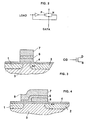
- FIG. 3 schematically illustrates the structure of a so-called stack gate cell.
- This stack gate cell has a source zone 1 and a drain zone 2 in a semiconductor substrate 3.
- the source zone 1 and the drain zone 2 are both n + -doped, while the semiconductor substrate 3 has a p-doping.
- the source zone 1 and the drain zone 2 and the channel region of the semiconductor substrate 3 between the source zone 1 and the drain zone 2 are provided with a tunnel oxide layer 4 made of, for example, silicon dioxide.
- a floating gate 5 made of, for example, polycrystalline silicon is located on the tunnel oxide layer 4 in the region between the drain zone 2 and the source zone 1.
- An intermediate polydielectric 6 and a control gate 7 are also arranged on this floating gate 5.
- FN tunnels For deleting and programming data, such Stack gate cell the so-called "Fowler-Nordheim tunnel" (FN tunnels) can be applied.
- FN tunnels Low-Nordheim tunnels
- 0 V is applied to drain zone 2 and +15 V.
- the control gate 7 applied.
- electrons tunnel out of the Channel area through the tunnel oxide layer 4 into the floating Gate 5.
- programming for example, 0 V is on the control gate 7 and +15 V at drain zone 2, what electrons from the floating gate 5 through the tunnel oxide layer 4 into the Drain zone 2 can tunnel.
- hot-e programming When programming with hot electrons (“hot-e programming") are to the control gate 7, for example +15 V, to the Drain zone 2 + 5V and applied to source zone 1 0V. Thereby electrons migrate from drain zone 2 to the source zone 1 and tunnel simultaneously through the tunnel oxide layer 4 in the floating gate 5.
- an EEPROM is programmable byte and erasable while a flash memory by hot electrons or FN tunnels programmable byte by byte and by FN tunnels can be deleted in blocks.
- FIG. 4 shows, as another type of memory cell, a so-called split-gate cell with a semiconductor substrate 3, an n + -doped source zone 1, an n + -doped drain zone 2, a tunnel oxide layer 4, a floating gate 5, an intermediate polydielectric 6 and a control gate 7.
- the "lowered" part of the control gate 7 is also referred to as the series gate 8, since the increased control gate 7 and the series gate 8 can be regarded as interconnected gates of two NMOS transistors connected in series.
- the stack cell shown in Fig. 3 is by a in this Figure shown on the right, "CG" the control gate 7, "D” the connection of the drain zone 2 and “S” the connection of source zone 1 means.
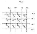
- Memory cells of the type shown in Fig. 3 can be a semiconductor memory with bit lines BL0, BL1, BL2, BL3 and word lines WL0, WL1, WL2 and WL3 form like this schematically is indicated in Fig. 5.
- high voltages are required can be selectively applied to selected word lines or bit lines to delete or to delete individual memory cells program.
- semiconductor memory arrays but also specially regulated voltages with a higher one Constancy than the supply voltage due to high voltages of for example, 15 V can be switched.
- bit lines for flash memories with negative programming voltage
- IEDM International Electron Device Meeting
- a control circuit is used to generate such control voltages needed that the desired voltages with high Should deliver consistency and a small footprint.
- control circuit according to EP 0 154 379 A2 contains a large number of PMOS transistors that are relatively large space requirement and lower electricity yield to have.
- a control circuit is the input mentioned type with the characterizing features of the claim 1 trained.
- the input circuit is composed of one with its source-drain path between a data input and a first data output lying first NMOS transistor and a series connection of two between ground and a second data output lying second and third NMOS transistors are formed, the gate of the second NMOS transistor with gate of the first NMOS transistor and gate of third NMOS transistor with source or drain of the first NMOS transistor are connected. It is expressly noted that such an input circuit is also separate from the Control circuit can be used when using simple Averaging generates a signal and a signal inverted to this should be.
- the control circuit according to the invention can be done with a few Realize components on a small area so that they are on narrowest space in the grid of the memory matrix of the semiconductor memory arrangement can be accommodated.
- the input circuit is made up of just three NMOS transistors, so that they are particularly easy and inexpensive to implement is what semiconductor memory devices or their Grid is of paramount importance. Since there are no PMOS transistors input circuit can be used in a common tub can be accommodated, which is an additional Space advantage means. As a result of the higher current yield of NMOS transistors compared to PMOS transistors can also make the entire circuit particularly small be interpreted.
- the locking circuit can advantageously be made there are two inverters connected in antiparallel.
- Fig. 1 shows the circuit structure of a drive circuit according to the invention.
- This control circuit consists of a Level converter circuit 10, a latch circuit (Latch) 11 and an input circuit 12.
- the level converter circuit 10 consists of PMOS transistors P1, P2 and NMOS transistors N4, N5 and has output connections D and DN on that with the bit lines or word lines of a semiconductor memory device are connected.
- the output lines D or DN represent depending on an input value of "1" or "0", which is connected to an input DATA, a voltage VPROG or 0 V are available.
- the output connection is DN complementary to the output terminal D and delivers 0 V or a voltage VPROG if there is a voltage at the output terminal D. V from VPROG or 0 V.
- VPROG an externally supplied voltage
- the transistors N4, N5, P1 and P2 the Feeding this voltage VPROG to the output connection D or DN controlled, the output DN complementary to the output D is, as has already been explained above.
- a level converter circuit associated with the level converter circuit 10 is similar, is from the aforementioned US-A-5,293,561 known per se.
- the level converter circuit 10 is the latch circuit 11 upstream, which consist of two antiparallel to each other Inverters I1 and I2 exist.
- an input circuit 12 made of three NMOS transistors N1 to N3.
- the data to be saved for example 5 V for a data value "1" are over a Input DATA fed to the input circuit.
- Source or drain of transistor N1 connected to input DATA which also applies to the gate of the transistor N3, the one with the transistor N2 is connected in series.
- Gates of transistors N1 and N2 are connected to one another and to a LOAD connection connected.
- the control circuit according to the invention is particularly well suited for data stored in a non-volatile semiconductor memory device should be programmed. These dates are buffered in the locking circuit 11, and there will be a regulated voltage VPROG for each bit line made available.
- the control circuit is in this Application provided separately for each bit line or word line.
- the data to be programmed is sent to the input line DATA created. With a positive pulse at the connection The data is then LOAD into the latch circuit 11 taken over.
- the signal at the output connection DN is there component to the signal at the output terminal D and delivers 0 V or a voltage VPROG if the voltage at Output terminal D has the value VPROG or 0 V.
- control circuit on a bit line and / or a word line for the general distribution of high voltages.
- the input circuit 12 is only made up of the three NMOS transistors N1, N2 and N3 built. It is special simple and inexpensive to implement, what kind of Memory grid circuits is of paramount importance. There no PMOS transistors can be used, this can Circuit part are generated in a common tub what means a considerable space advantage.
- the input circuit Depending on the input date, 12 pulls the node on the right in FIG. 1 the locking circuit via the transistor N (at the input terminal DATA is "0") at 0 V or the left node to 0 V via transistors N2 and N3.
- the input circuit 12 can be compared to PMOS transistors be designed to be particularly small. Specifically, the sum of the Width of the transistors N2 and N3 may only be as large as the width of a PMOS transistor with a corresponding one CMOS transfer gate (see Fig. 2). For control the input circuit 12 is still only one signal LOAD needed. An additional inverted signal like this is required in itself with a CMOS transfer gate not to be used.
- the control circuit according to the invention does not require an additional one Input inverter for controlling the transistors N4 and N5, but it will do the job of Inverters I1 and I2 of the interlock circuit used.
- the advantageous combination of the locking circuit 11 with the level converter circuit 10 thus saves components and is therefore particularly suitable for use in area-critical Memory grid circuits suitable.
Landscapes
- Read Only Memory (AREA)
- Static Random-Access Memory (AREA)
- Non-Volatile Memory (AREA)
- Semiconductor Memories (AREA)
Abstract
Description
Die vorliegende Erfindung betrifft eine Ansteuerschaltung für eine nichtflüchtige Halbleiterspeicheranordnung, mit einer Pegelwandlerschaltung, die einen Ausgangswert und einen zu diesem Ausgangswert komplementären Ausgangswert an eine Bitleitung und/oder eine Wortleitung der Halbleiterspeicheranordnung anlegt, und mit einer zwischen einer Eingabeschaltung und der Pegelwandlerschaltung liegenden Verriegelungsschaltung (Latch), die die in der Halbleiterspeicheranordnung zu speichernden Daten zwischenspeichert.The present invention relates to a control circuit for a non-volatile semiconductor memory device, with a Level converter circuit, which has an output value and a this output value complementary output value to a bit line and / or a word line of the semiconductor memory arrangement creates, and with one between an input circuit and the locking circuit lying level converter circuit (Latch) that in the semiconductor memory device data to be stored temporarily.
Eine solche Ansteuerschaltung ist aus der EP 0 154 379 A2 bekannt.Such a control circuit is known from EP 0 154 379 A2.
Nichflüchtige Halbleiter-Speicheranordnungen, wie beispielsweise Flash-Speicher und elektrisch löschbare programmierbare Festwertspeicher (EEPROM) benötigen zum Aufbringen bzw. Entfernen von Ladungen und damit Daten aus den einzelnen Speicherzellen Spannungen von typischerweise 15 V. Diese Spannungen, die die normale Versorgungsspannung Vdd, die in der Größenordnung 5 V liegt, wesentlich übersteigen, werden im folgenden auch als "Hochspannungen" bezeichnet. Je nach der Betriebsart werden die Hochspannungen an Wortleitungen oder Bitleitungen oder auch an Wortleitungen und Bitleitungen einer Halbleiter-Speicheranordnung angelegt.Non-volatile semiconductor memory devices, such as Flash memory and electrically erasable programmable Read-only memories (EEPROM) need to be attached or removed of charges and thus data from the individual memory cells Voltages of typically 15 V. These voltages, which is the normal supply voltage Vdd, which is of the order of magnitude 5 V lies, significantly exceed, are in the following also referred to as "high voltages". Depending on the operating mode are the high voltages on word lines or Bit lines or on word lines and bit lines one Semiconductor memory array created.
Fig. 3 veranschaulicht schematisch den Aufbau einer sogenannten
Stapel-Gate-Zelle. Diese Stapel-Gate-Zelle weist eine
Source-Zone 1 und eine Drain-Zone 2 in einem Halbleitersubstrat
3 auf. Die Source-Zone 1 und die Drain-Zone 2 sind beide
n+-dotiert, während das Halbleitersubstrat 3 eine p-Dotierung
hat. Die Source-Zone 1 und die Drain-Zone 2 sowie der
Kanalbereich des Halbleitersubstrates 3 zwischen der Source-Zone
1 und der Drain-Zone 2 sind mit einer Tunneloxidschicht
4 aus beispielsweise Siliciumdioxid versehen. Auf der Tunneloxidschicht
4 befindet sich im Bereich zwischen der Drain-Zone
2 und der Source-Zone 1 ein Floating Gate 5 aus beispielsweise
polykristallinem Silicium. Auf diesem Floating
Gate 5 sind noch ein Zwischenpolydielektrikum 6 und ein Steuergate
7 angeordnet.3 schematically illustrates the structure of a so-called stack gate cell. This stack gate cell has a
Zum Löschen und Programmieren von Daten kann bei einer solchen
Stapel-Gate-Zelle das sogenannte "Fowler-Nordheim-Tunneln"
(FN-Tunneln) angewandt werden. Bei einem Löschvorgang
werden beispielsweise 0 V an die Drain-Zone 2 und +15 V an
das Steuergate 7 angelegt. Dann tunneln Elektronen aus dem
Kanalbereich durch die Tunneloxidschicht 4 in das Floating
Gate 5. Beim Programmieren liegen beispielsweise 0 V am Steuergate
7 und +15 V an der Drain-Zone 2, was Elektronen aus
dem Floating Gate 5 durch die Tunneloxidschicht 4 in die
Drain-Zone 2 tunneln läßt. Es ist aber auch möglich, zum Programmieren
beispielsweise -11 V an das Steuergate 7 und +4 V
an die Drain-Zone 2 anzulegen. Auch hierdurch werden Elektronen
veranlaßt, aus dem Floating Gate 5 in die Drain-Zone 2 zu
tunneln.For deleting and programming data, such
Stack gate cell the so-called "Fowler-Nordheim tunnel"
(FN tunnels) can be applied. When deleting
For example, 0 V is applied to
Beim Programmieren mit heißen Elektronen ("hot-e-Programmieren")
werden an das Steuergate 7 beispielsweise +15 V, an die
Drain-Zone 2 +5V und an die Source-Zone 1 0 V angelegt. Dadurch
wandern Elektronen aus der Drain-Zone 2 zur Source-Zone
1 und tunneln gleichzeitig durch die Tunneloxidschicht 4 in
das Floating Gate 5.When programming with hot electrons ("hot-e programming")
are to the
Ein EEPROM ist bekanntlich byteweise programmierbar und löschbar, während ein Flash-Speicher durch heiße Elektronen oder FN-Tunneln byteweise programmierbar und durch FN-Tunneln blockweise löschbar ist.As is well known, an EEPROM is programmable byte and erasable while a flash memory by hot electrons or FN tunnels programmable byte by byte and by FN tunnels can be deleted in blocks.
Fig. 4 zeigt als anderen Speicherzellentyp eine sogenannte
Split-Gate-Zelle mit einem Halbleitersubstrat 3, einer n+-dotierten
Source-Zone 1, einer n+-dotierten Drain-Zone 2, einer
Tunneloxidschicht 4, einem Floating Gate 5, einem Zwischenpolydielektrikum
6 und einem Steuergate 7. Der "abgesenkte"
Teil des Steuergates 7 wird auch als Seriengate 8 bezeichnet,
da das erhöhte Steuergate 7 und das Seriengate 8
als miteinander verbundene Gates von zwei in Reihe geschalteten
NMOS-Transistoren angesehen werden können.FIG. 4 shows, as another type of memory cell, a so-called split-gate cell with a
Die in Fig. 3 gezeigte Stapelzelle wird durch ein in dieser
Figur rechts dargestelltes Symbol wiedergegeben, wobei "CG"
das Steuergate 7, "D" den Anschluß der Drain-Zone 2 und "S"
den Anschluß der Source-Zone 1 bedeutet.The stack cell shown in Fig. 3 is by a in this
Figure shown on the right, "CG"
the
Speicherzellen der in Fig. 3 gezeigten Art können einen Halbleiterspeicher mit Bitleitungen BL0, BL1, BL2, BL3 und Wortleitungen WL0, WL1, WL2 und WL3 bilden, wie dies schematisch in Fig. 5 angedeutet ist.Memory cells of the type shown in Fig. 3 can be a semiconductor memory with bit lines BL0, BL1, BL2, BL3 and word lines WL0, WL1, WL2 and WL3 form like this schematically is indicated in Fig. 5.
Bei einer Halbleiter-Speicheranordnung müssen Hochspannungen selektiv an ausgewählte Wortleitungen bzw. Bitleitungen anlegbar sein, um einzelne Speicherzellen zu löschen oder zu programmieren. Neben Halbleiter-Speicheranordnungen müssen aber auch speziell geregelte Spannungen mit einer höheren Konstanz als die Versorgungsspannung durch Hochspannungen von beispielsweise 15 V geschaltet werden.In a semiconductor memory device, high voltages are required can be selectively applied to selected word lines or bit lines to delete or to delete individual memory cells program. In addition to semiconductor memory arrays but also specially regulated voltages with a higher one Constancy than the supply voltage due to high voltages of for example, 15 V can be switched.
Ein wichtiger Anwendungsfall ist beispielsweise die Ansteuerung der Bitleitungen bei Flash-Speichern mit negativer Programmierspannung (vergleiche hierzu beispielsweise R. Heinrich, W. Heinrigs, G. Tempel, J. Winnerl, T. Zettler, in Proc. of the International Electron Device Meeting (IEDM), 1993, Seiten 445 bis 448). Zur Erzielung konstanter Programmierbedingungen wird hier beispielsweise die Bitleitungsspannung auf 5 V geregelt, während an den Wortleitungen -12 V anliegen. Auch solche geregelte Spannungen von beispielsweise 5 V, die unter der Versorgungsspannung von 5,5 V liegen, werden im folgenden unter "Hochspannung" verstanden.An important application is, for example, control the bit lines for flash memories with negative programming voltage (see for example R. Heinrich, W. Heinrigs, G. Tempel, J. Winnerl, T. Zettler, in Proc. of the International Electron Device Meeting (IEDM), 1993, pages 445 to 448). To achieve constant programming conditions for example, the bit line voltage regulated to 5 V, while -12 V are present on the word lines. Such regulated voltages of, for example, 5 V, which are below the supply voltage of 5.5 V. hereinafter referred to as "high voltage".
Zur Erzeugung derartiger Ansteuerspannungen wird eine Ansteuerschaltung benötigt, die die gewünschten Spannungen mit hoher Konstanz und geringem Flächenbedarf liefern soll. A control circuit is used to generate such control voltages needed that the desired voltages with high Should deliver consistency and a small footprint.
Im Einzelnen ist in der US-A-5, 293, 561 eine Ansteuerschaltung mit einer Spannungsverteilerschaltung für die separate Versorgung von Speicherfeld und Speicher für Redundanzeinstellungen mit Hochspannungen beschrieben. Diese bekannte Ansteuerschaltung hat insbesondere eine Pegelwandlerschaltung, die einen Ausgangswert und einen zu diesem Ausgangswert komplementären Ausgangswert an eine Halbleiter-Speicheranordnung anzulegen vermag.Specifically, there is a drive circuit in US-A-5, 293, 561 with a voltage distribution circuit for separate supply of memory field and memory for redundancy settings described with high voltages. This known control circuit in particular has a level converter circuit that an initial value and one complementary to this initial value Output value to a semiconductor memory device is able to invest.
Es hat sich aber gezeigt, daß die bekannte Ansteuerschaltung gemäß der US-A-5,293,561 für die Bitleitungsansteuerung wenig geeignet ist, da sie keine Zwischenspeicherung von Daten ermöglicht. Außerdem enthält die bekannte Ansteuerschaltung NMOS-Transistoren vom Verarmungstyp, die als zusätzliche Bauelemente einen beträchtlichen technologischen Aufwand bedingen.However, it has been shown that the known control circuit little in accordance with US-A-5,293,561 for bit line driving is suitable because it does not allow data to be cached. It also contains the known control circuit Depletion-type NMOS transistors used as additional components require considerable technological effort.
Die Ansteuerschaltung gemäß der EP 0 154 379 A2 enthält hingegen eine große Zahl von PMOS-Transistoren, die einen relativ großen Flächenbedarf und eine geringere Stromergiebigkeit haben.The control circuit according to EP 0 154 379 A2, however, contains a large number of PMOS transistors that are relatively large space requirement and lower electricity yield to have.
Es ist daher Aufgabe der vorliegenden Erfindung, eine Ansteuerschaltung für eine nichtflüchtige Halbleiter-Speicheranordnung zu schaffen, die mit möglichst wenigen Bauelementen auf kleiner Fläche realisierbar ist, so daß sie auf engstem Raum im Raster der Speichermatrix der HalbleiterSpeicheranordnung aufgebaut werden kann, und die Ansteuerspannungen mit hoher Konstanz auch im Hochspannungsbereich abzugeben vermag.It is therefore an object of the present invention to provide a control circuit for a non-volatile semiconductor memory arrangement which can be implemented with as few components as possible in a small area, so that it can be built up in the smallest space in the grid of the memory matrix of the semiconductor memory arrangement, and the control voltages can deliver high consistency even in the high-voltage range.
Zur Lösung dieser Aufgabe ist eine Ansteuerschaltung der eingangs
genannten Art mit den kennzeichnenden Merkmalen des Anspruchs
1 ausgebildet.To solve this problem, a control circuit is the input
mentioned type with the characterizing features of the
Die Eingabeschaltung ist in erfindungsgemäßer Weise aus einem mit seiner Source-Drain-Strecke zwischen einem Dateneingang und einem ersten Datenausgang liegenden ersten NMOS-Transistor und einer Reihenschaltung aus zwei zwischen Masse und einem zweiten Datenausgang liegenden zweiten und dritten NMOS-Transistoren gebildet, wobei Gate des zweiten NMOS-Transistors mit Gate des ersten NMOS-Transistors und Gate des dritten NMOS-Transistors mit Source bzw. Drain des ersten NMOS-Transistors verbunden sind. Es sei ausdrücklich angemerkt, daß eine solche Eingabeschaltung auch getrennt von der Ansteuerschaltung eingesetzt werden kann, wenn mit einfachen Mitteln ein Signal und ein zu diesem invertiertes Signal erzeugt werden sollen.In the manner according to the invention, the input circuit is composed of one with its source-drain path between a data input and a first data output lying first NMOS transistor and a series connection of two between ground and a second data output lying second and third NMOS transistors are formed, the gate of the second NMOS transistor with gate of the first NMOS transistor and gate of third NMOS transistor with source or drain of the first NMOS transistor are connected. It is expressly noted that such an input circuit is also separate from the Control circuit can be used when using simple Averaging generates a signal and a signal inverted to this should be.
Die erfindungsgemäße Ansteuerschaltung läßt sich mit wenigen Bauelementen auf kleiner Fläche realisieren, so daß sie auf engstem Raum im Raster der Speichermatrix der Halbleiter-Speicheranordnung untergebracht werden kann. Die Eingabeschaltung ist aus lediglich drei NMOS-Transistoren aufgebaut, so daß sie besonders einfach und flächengünstig zu realisieren ist, was für Halbleiter-Speicheranordnungen bzw. deren Raster von höchster Bedeutung ist. Da hier keine PMOS-Transistoren zum Einsatz kommen, kann die Eingabeschaltung in einer gemeinsamen Wanne untergebracht werden, was einen zusätzlichen Flächenvorteil bedeutet. Infolge der höheren Stromergiebigkeit der NMOS-Transistoren im Vergleich zu PMOS-Transistoren kann zudem die gesamte Schaltung besonders klein ausgelegt werden.The control circuit according to the invention can be done with a few Realize components on a small area so that they are on narrowest space in the grid of the memory matrix of the semiconductor memory arrangement can be accommodated. The input circuit is made up of just three NMOS transistors, so that they are particularly easy and inexpensive to implement is what semiconductor memory devices or their Grid is of paramount importance. Since there are no PMOS transistors input circuit can be used in a common tub can be accommodated, which is an additional Space advantage means. As a result of the higher current yield of NMOS transistors compared to PMOS transistors can also make the entire circuit particularly small be interpreted.
Die Verriegelungsschaltung kann in vorteilhafter Weise aus zwei antiparallel geschalteten Invertern bestehen.The locking circuit can advantageously be made there are two inverters connected in antiparallel.
Nachfolgend wird die Erfindung anhand der Zeichnungen näher erläutert. Es zeigen:
- Fig. 1
- ein Schaltbild der erfindungsgemäßen Ansteuerschaltung;
- Fig. 2
- ein CMOS-Transfergate;
- Fig. 3
- ein Schnittbild einer Stapel-Gate-Zelle;
- Fig. 4
- ein Schnittbild einer Split-Gate-Zelle, und
- Fig. 5
- eine Speicherzellenmatrix mit Wortleitungen und Bitleitungen.
- Fig. 1
- a circuit diagram of the control circuit according to the invention;
- Fig. 2
- a CMOS transfer gate;
- Fig. 3
- a sectional view of a stack gate cell;
- Fig. 4
- a sectional view of a split gate cell, and
- Fig. 5
- a memory cell matrix with word lines and bit lines.
Die Fig. 3 bis 5 sind bereits eingangs erläutert worden.3 to 5 have already been explained at the beginning.
Fig. 1 zeigt den Schaltungsaufbau einer erfindungsgemäßen Ansteuerschaltung.
Diese Ansteuerschaltung besteht aus einer
Pegelwandlerschaltung 10, einer Verriegelungsschaltung
(Latch) 11 und einer Eingabeschaltung 12. Die Pegelwandlerschaltung
10 besteht aus PMOS-Transistoren P1, P2 und NMOS-Transistoren
N4, N5 und weist Ausgangsanschlüsse D bzw. DN
auf, die mit den Bitleitungen bzw. Wortleitungen einer Halbleiter-Speicheranordnung
verbunden sind. Die Ausgangsleitungen
D bzw. DN stellen je nach einem Eingangswert von "1" bzw.
"0", der an einem Eingang DATA liegt, eine Spannung VPROG
bzw. 0 V zur Verfügung. Dabei ist der Ausgangsanschluß DN
komplementär zu dem Ausgangsanschluß D und liefert 0 V bzw.
eine Spannung VPROG, wenn am Ausgangsanschluß D eine Spannung
V von VPROG bzw. 0 V anliegt.Fig. 1 shows the circuit structure of a drive circuit according to the invention.
This control circuit consists of a
An Drain bzw. Source der PMOS-Transistoren P1 bzw. P2 liegt eine von außen zugeführte Spannung VPROG von beispielsweise 15 V. Mittels der Transistoren N4, N5, P1 und P2 wird die Einspeisung dieser Spannung VPROG zum Ausgangsanschluß D bzw. DN gesteuert, wobei der Ausgang DN komplementär zum Ausgang D ist, wie dies oben bereits erläutert wurde.Is on the drain or source of the PMOS transistors P1 and P2 an externally supplied voltage VPROG, for example 15 V. Using the transistors N4, N5, P1 and P2, the Feeding this voltage VPROG to the output connection D or DN controlled, the output DN complementary to the output D is, as has already been explained above.
Eine Pegelwandlerschaltung, die zu der Pegelwandlerschaltung
10 ähnlich ist, ist aus der bereits genannten US-A-5,293,561
an sich bekannt.A level converter circuit associated with the
Der Pegelwandlerschaltung 10 ist die Verriegelungsschaltung
11 vorgeschaltet, die aus zwei antiparallel zueinander liegenden
Invertern I1 und I2 besteht. Vor dieser Verriegelungsschaltung
11 liegt eine Eingabeschaltung 12 aus drei NMOS-Transistoren
N1 bis N3. Die zu speichernden Daten, also beispielsweise
5 V für einen Datenwert "1", werden über einen
Eingang DATA der Eingabeschaltung zugeführt. Dabei ist Source
bzw. Drain des Transistors N1 mit dem Eingang DATA verbunden,
was auch für Gate des Transistors N3 gilt, der mit dem Transistor
N2 in Reihe geschaltet ist. Gates der Transistoren N1
und N2 sind miteinander verbunden und an einen Anschluß LOAD
angeschlossen. Liegen an dem Anschluß LOAD beispielsweise 5
V, so leiten die Transistoren N1 und N2, so daß 0 V an dem in
Fig. 1 linken Eingang der Verriegelungsschaltung 11 liegen,
während beispielsweise ein Datensignal "1" von 5 V über den
Transistor N1 dem in Fig. 1 rechten Eingang der Verriegelungsschaltung
11 (vermindert um die Einsatzspannung des
Transistors N1) zugeführt wird.The
Die erfindungsgemäße Ansteuerschaltung ist besonders gut geeignet
für Daten, welche in eine nichtflüchtige Halbleiter-Speicheranordnung
programmiert werden sollen. Diese Daten
werden in der Verriegelungsschaltung 11 zwischengespeichert,
und es wird eine geregelte Spannung VPROG für jede Bitleitung
zur Verfügung gestellt. Die Ansteuerschaltung wird bei dieser
Anwendung getrennt für jede Bitleitung bzw. Wortleitung vorgesehen.
Die zu programmierenden Daten werden an die Eingangsleitung
DATA angelegt. Durch einen positiven Puls am Anschluß
LOAD werden die Daten sodann in die Verriegelungsschaltung
11 übernommen. An den Ausgangsanschlüssen D und DN
stellt die Pegelwandlerschaltung 10 dann je nach Eingangswert
"1" bzw. "0" am Eingangsanschluß DATA die Spannung VPROG bzw.
0 V zur Verfügung. Das Signal am Ausgangsanschluß DN ist dabei
kompelementär zu dem Signal am Ausgangsanschluß D und
liefert 0 V bzw. eine Spannung VPROG, wenn die Spannung am
Ausgangsanschluß D den Wert VPROG bzw. 0 V hat. The control circuit according to the invention is particularly well suited
for data stored in a non-volatile semiconductor memory device
should be programmed. These dates
are buffered in the locking
Selbstverständlich kann die erfindungsgemäße Ansteuerschaltung an einer Bitleitung und/oder einer Wortleitung für die allgemeine Verteilung von Hochspannungen eingesetzt werden.Of course, the control circuit according to the invention on a bit line and / or a word line for the general distribution of high voltages.
Die Eingabeschaltung 12 ist lediglich aus den drei NMOS-Transistoren
N1, N2 und N3 aufgebaut. Sie ist damit besonders
einfach und flächendeckend günstig zu realisieren, was für
Speicher-Rasterschaltungen von höchster Bedeutung ist. Da
keine PMOS-Transistoren zum Einsatz kommen, kann dieser
Schaltungsteil in einer gemeinsamen Wanne erzeugt werden, was
einen erheblichen Flächenvorteil bedeutet. Die Eingabeschaltung
12 zieht je nach Eingabedatum den in Fig. 1 rechten Knoten
der Verriegelungsschaltung über den Transistor N (am Eingangsanschluß
DATA liegt "0") auf 0 V oder den linken Knoten
über die Transistoren N2 und N3 auf 0 V.The
Durch die höhere Stromergiebigkeit von NMOS-Transistoren im
Vergleich zu PMOS-Transistoren kann die Eingabeschaltung 12
besonders klein ausgelegt werden. Speziell muß die Summe der
Weite der Transistoren N2 und N3 nur maximal so groß sein wie
die Weite eines PMOS-Transistors mit einem entsprechenden
CMOS-Transfergate (vergleiche Fig. 2). Für die Ansteuerung
der Eingabeschaltung 12 wird weiterhin nur das eine Signal
LOAD benötigt. Ein zusätzliches invertiertes Signal, wie es
an sich bei einem CMOS-Transfergate erforderlich ist, braucht
nicht verwendet zu werden.Due to the higher current yield of NMOS transistors in
The
Die erfindungsgemäße Ansteuerschaltung benötigt keinen zusätzlichen
Eingangsinverter für die Ansteuerung der Transistoren
N4 und N5, sondern es wird hierfür die Funktion der
Inverter I1 und I2 der Verriegelungsschaltung ausgenutzt. Die
vorteilhafte Kombination der Verriegelungsschaltung 11 mit
der Pegelwandlerschaltung 10 spart somit Bauelemente ein und
ist deshalb besonders für den Einsatz in flächenkritischen
Speicherrasterschaltungen geeignet.The control circuit according to the invention does not require an additional one
Input inverter for controlling the transistors
N4 and N5, but it will do the job of
Inverters I1 and I2 of the interlock circuit used. The
advantageous combination of the locking
Claims (2)
- Drive circuit for a non-volatile semiconductor storage arrangement, having a level converter circuit (10) which applies an output value (D) and an output value (DN) complementary to this output value to a bit line and/or a word line of the semiconductor storage arrangement, with a latch circuit (11) which lies between an input circuit (12) and the level converter circuit (10) and temporarily stores the data to be stored in the semiconductor storage arrangement, characterized in that the input cicuit (12) consists of a first NMOS transistor (N1) with its source-drain path lying between a data input (DATA) and a first data output connected to a control input of the level converter circuit (10), and a series circuit consisting of two second and third NMOS transistors (N2, N3) lying between earth and a second data output which is connected to a control connection of the level converter circuit (10) and is complementary to the control connection, the gate of the second NMOS transistor (N2) being connected to the gate of the first NMOS transistor (N1) and the gate of the third NMOS transistor (N3) being connected to the data input (DATA).
- Drive circuit according to Claim 1, characterized in that the latch circuit (11) consists of two inverters (I1, I2) connected in antiparallel.
Applications Claiming Priority (3)
| Application Number | Priority Date | Filing Date | Title |
|---|---|---|---|
| DE19725181 | 1997-06-13 | ||
| DE19725181A DE19725181A1 (en) | 1997-06-13 | 1997-06-13 | Drive circuit for non-volatile semiconductor memory device |
| PCT/DE1998/001560 WO1998058384A1 (en) | 1997-06-13 | 1998-06-08 | Control circuit for a non-volatile semi-conductor memory system |
Publications (2)
| Publication Number | Publication Date |
|---|---|
| EP0988633A1 EP0988633A1 (en) | 2000-03-29 |
| EP0988633B1 true EP0988633B1 (en) | 2001-05-09 |
Family
ID=7832475
Family Applications (1)
| Application Number | Title | Priority Date | Filing Date |
|---|---|---|---|
| EP98936116A Expired - Lifetime EP0988633B1 (en) | 1997-06-13 | 1998-06-08 | Control circuit for a non-volatile semi-conductor memory system |
Country Status (12)
| Country | Link |
|---|---|
| US (1) | US6137315A (en) |
| EP (1) | EP0988633B1 (en) |
| JP (1) | JP3399547B2 (en) |
| KR (1) | KR20010013737A (en) |
| CN (1) | CN1124617C (en) |
| AT (1) | ATE201112T1 (en) |
| BR (1) | BR9810100A (en) |
| DE (2) | DE19725181A1 (en) |
| ES (1) | ES2157666T3 (en) |
| RU (1) | RU2221286C2 (en) |
| UA (1) | UA42887C2 (en) |
| WO (1) | WO1998058384A1 (en) |
Families Citing this family (7)
| Publication number | Priority date | Publication date | Assignee | Title |
|---|---|---|---|---|
| DE19921868C2 (en) * | 1999-05-11 | 2001-03-15 | Siemens Ag | Circuit arrangement for checking the states of a memory device |
| US7440311B2 (en) * | 2006-09-28 | 2008-10-21 | Novelics, Llc | Single-poly non-volatile memory cell |
| US7554860B1 (en) | 2007-09-21 | 2009-06-30 | Actel Corporation | Nonvolatile memory integrated circuit having assembly buffer and bit-line driver, and method of operation thereof |
| CN103036548B (en) | 2007-12-28 | 2016-01-06 | 夏普株式会社 | Semiconductor device and display unit |
| CN101878592B (en) * | 2007-12-28 | 2012-11-07 | 夏普株式会社 | Semiconductor device and display device |
| CN101965607B (en) | 2007-12-28 | 2013-08-14 | 夏普株式会社 | Auxiliary capacity wiring driving circuit and display device |
| JP4981928B2 (en) | 2007-12-28 | 2012-07-25 | シャープ株式会社 | Display drive circuit and display device |
Family Cites Families (8)
| Publication number | Priority date | Publication date | Assignee | Title |
|---|---|---|---|---|
| US4599707A (en) * | 1984-03-01 | 1986-07-08 | Signetics Corporation | Byte wide EEPROM with individual write circuits and write prevention means |
| US4716312A (en) * | 1985-05-07 | 1987-12-29 | California Institute Of Technology | CMOS logic circuit |
| US4654547A (en) * | 1985-06-28 | 1987-03-31 | Itt Corporation | Balanced enhancement/depletion mode gallium arsenide buffer/comparator circuit |
| FR2604554B1 (en) * | 1986-09-30 | 1988-11-10 | Eurotechnique Sa | SECURITY DEVICE FOR PROGRAMMING AN ELECTRICALLY PROGRAMMABLE NON-VOLATILE MEMORY |
| JP2773786B2 (en) * | 1991-02-15 | 1998-07-09 | 日本電気アイシーマイコンシステム株式会社 | Write voltage generation circuit |
| JP3173247B2 (en) * | 1993-09-29 | 2001-06-04 | ソニー株式会社 | Level shifter |
| US5682345A (en) * | 1995-07-28 | 1997-10-28 | Micron Quantum Devices, Inc. | Non-volatile data storage unit method of controlling same |
| JP3404712B2 (en) * | 1996-05-15 | 2003-05-12 | 株式会社東芝 | Nonvolatile semiconductor memory device and writing method thereof |
-
1997
- 1997-06-13 DE DE19725181A patent/DE19725181A1/en not_active Ceased
-
1998
- 1998-06-08 DE DE59800692T patent/DE59800692D1/en not_active Expired - Lifetime
- 1998-06-08 AT AT98936116T patent/ATE201112T1/en active
- 1998-06-08 ES ES98936116T patent/ES2157666T3/en not_active Expired - Lifetime
- 1998-06-08 WO PCT/DE1998/001560 patent/WO1998058384A1/en not_active Application Discontinuation
- 1998-06-08 RU RU2000100927/09A patent/RU2221286C2/en not_active IP Right Cessation
- 1998-06-08 EP EP98936116A patent/EP0988633B1/en not_active Expired - Lifetime
- 1998-06-08 JP JP50354499A patent/JP3399547B2/en not_active Expired - Fee Related
- 1998-06-08 UA UA99126788A patent/UA42887C2/en unknown
- 1998-06-08 BR BR9810100-5A patent/BR9810100A/en not_active IP Right Cessation
- 1998-06-08 KR KR1019997011752A patent/KR20010013737A/en not_active Application Discontinuation
- 1998-06-08 CN CN98806144A patent/CN1124617C/en not_active Expired - Fee Related
-
1999
- 1999-12-13 US US09/460,346 patent/US6137315A/en not_active Expired - Fee Related
Also Published As
| Publication number | Publication date |
|---|---|
| ATE201112T1 (en) | 2001-05-15 |
| KR20010013737A (en) | 2001-02-26 |
| BR9810100A (en) | 2000-08-08 |
| RU2221286C2 (en) | 2004-01-10 |
| CN1260901A (en) | 2000-07-19 |
| EP0988633A1 (en) | 2000-03-29 |
| US6137315A (en) | 2000-10-24 |
| CN1124617C (en) | 2003-10-15 |
| DE59800692D1 (en) | 2001-06-13 |
| ES2157666T3 (en) | 2001-08-16 |
| JP2001505350A (en) | 2001-04-17 |
| WO1998058384A1 (en) | 1998-12-23 |
| UA42887C2 (en) | 2001-11-15 |
| JP3399547B2 (en) | 2003-04-21 |
| DE19725181A1 (en) | 1999-02-25 |
Similar Documents
| Publication | Publication Date | Title |
|---|---|---|
| DE4000787C2 (en) | ELECTRICALLY ERASABLE AND PROGRAMMABLE SEMICONDUCTOR STORAGE DEVICE | |
| DE3929816C2 (en) | Electrically erasable and programmable semiconductor memory device and method for erasing and programming this semiconductor memory device | |
| DE4036973C2 (en) | Circuit for generating an erase or programming voltage in a semiconductor memory circuit that is higher than an externally supplied supply voltage | |
| DE4232025C2 (en) | Electrically erasable and programmable non-volatile semiconductor memory with automatic write check controller | |
| DE4035660C2 (en) | Electrically programmable memory device and method for accessing / programming memory cells | |
| DE4233248C2 (en) | Non-volatile semiconductor memory device and method for erasing data in blocks in a non-volatile semiconductor memory device | |
| DE69434550T2 (en) | Non-volatile semiconductor memory device which reduces the requirements for the dielectric strength | |
| DE4119394C2 (en) | Nonvolatile semiconductor memory device and data erasure method therefor | |
| DE69636178T2 (en) | Method for erasing a Flash EEPROM memory cell | |
| DE4343722C2 (en) | Precision reference voltage circuit suitable for use in computer systems | |
| DE4014117C2 (en) | ||
| DE3934303C2 (en) | Address decoder for non-volatile memories | |
| DE60303511T2 (en) | PROCEDURE FOR DELETING A FLASH MEMORY USING A PRE-ERRING PROCEDURE | |
| DE3032657A1 (en) | NON-VOLATILE, ELECTRICALLY CHANGEABLE STATIC SEMICONDUCTOR STORAGE ARRANGEMENT WITH OPTIONAL ACCESS. | |
| DE2742526A1 (en) | ELECTRICALLY PROGRAMMABLE MOS FIXED VALUE MEMORY | |
| DE4213741C2 (en) | Memory matrix with memory cells arranged in rows and columns | |
| DE4040492A1 (en) | AUTOMATIC CLEAR OPTIMIZATION CIRCUIT FOR AN ELECTRICALLY CLEAR AND PROGRAMMABLE SEMICONDUCTOR STORAGE AND AUTOMATIC CLEAR OPTIMIZATION METHOD | |
| DE102004063581A1 (en) | Semiconductor element | |
| DE3035484A1 (en) | NON-VOLATILE SEMICONDUCTOR MEMORY | |
| DE2514582C2 (en) | CIRCUIT FOR GENERATING READING PULSES | |
| EP0100772B1 (en) | Electrically programmable memory array | |
| DE2347968A1 (en) | ASSOCIATIVE MEMORY CIRCUIT | |
| DE60003451T2 (en) | WORDLINE SIGNALS OF A FLASH STORAGE REMAIN LOSS EVERYWHERE ON THE CHIP | |
| EP0988633B1 (en) | Control circuit for a non-volatile semi-conductor memory system | |
| DE4135032A1 (en) | EEPROM with memory cells contg. MOS with charge layer and control gate - has transistor with drain breakdown voltage adjuster for specified operational range |
Legal Events
| Date | Code | Title | Description |
|---|---|---|---|
| PUAI | Public reference made under article 153(3) epc to a published international application that has entered the european phase |
Free format text: ORIGINAL CODE: 0009012 |
|
| 17P | Request for examination filed |
Effective date: 19991206 |
|
| AK | Designated contracting states |
Kind code of ref document: A1 Designated state(s): AT CH DE ES FR GB IT LI |
|
| GRAG | Despatch of communication of intention to grant |
Free format text: ORIGINAL CODE: EPIDOS AGRA |
|
| GRAG | Despatch of communication of intention to grant |
Free format text: ORIGINAL CODE: EPIDOS AGRA |
|
| GRAH | Despatch of communication of intention to grant a patent |
Free format text: ORIGINAL CODE: EPIDOS IGRA |
|
| 17Q | First examination report despatched |
Effective date: 20000929 |
|
| GRAH | Despatch of communication of intention to grant a patent |
Free format text: ORIGINAL CODE: EPIDOS IGRA |
|
| GRAA | (expected) grant |
Free format text: ORIGINAL CODE: 0009210 |
|
| AK | Designated contracting states |
Kind code of ref document: B1 Designated state(s): AT CH DE ES FR GB IT LI |
|
| REF | Corresponds to: |
Ref document number: 201112 Country of ref document: AT Date of ref document: 20010515 Kind code of ref document: T |
|
| REG | Reference to a national code |
Ref country code: CH Ref legal event code: NV Representative=s name: SIEMENS SCHWEIZ AG Ref country code: CH Ref legal event code: EP |
|
| REF | Corresponds to: |
Ref document number: 59800692 Country of ref document: DE Date of ref document: 20010613 |
|
| ITF | It: translation for a ep patent filed |
Owner name: STUDIO JAUMANN P. & C. S.N.C. |
|
| REG | Reference to a national code |
Ref country code: ES Ref legal event code: FG2A Ref document number: 2157666 Country of ref document: ES Kind code of ref document: T3 |
|
| GBT | Gb: translation of ep patent filed (gb section 77(6)(a)/1977) |
Effective date: 20010730 |
|
| ET | Fr: translation filed | ||
| REG | Reference to a national code |
Ref country code: GB Ref legal event code: IF02 |
|
| PLBE | No opposition filed within time limit |
Free format text: ORIGINAL CODE: 0009261 |
|
| STAA | Information on the status of an ep patent application or granted ep patent |
Free format text: STATUS: NO OPPOSITION FILED WITHIN TIME LIMIT |
|
| 26N | No opposition filed | ||
| PGFP | Annual fee paid to national office [announced via postgrant information from national office to epo] |
Ref country code: CH Payment date: 20030520 Year of fee payment: 6 |
|
| PGFP | Annual fee paid to national office [announced via postgrant information from national office to epo] |
Ref country code: ES Payment date: 20030617 Year of fee payment: 6 |
|
| PG25 | Lapsed in a contracting state [announced via postgrant information from national office to epo] |
Ref country code: ES Free format text: LAPSE BECAUSE OF NON-PAYMENT OF DUE FEES Effective date: 20040609 |
|
| PG25 | Lapsed in a contracting state [announced via postgrant information from national office to epo] |
Ref country code: LI Free format text: LAPSE BECAUSE OF NON-PAYMENT OF DUE FEES Effective date: 20040630 Ref country code: CH Free format text: LAPSE BECAUSE OF NON-PAYMENT OF DUE FEES Effective date: 20040630 |
|
| REG | Reference to a national code |
Ref country code: CH Ref legal event code: PL |
|
| PG25 | Lapsed in a contracting state [announced via postgrant information from national office to epo] |
Ref country code: IT Free format text: LAPSE BECAUSE OF NON-PAYMENT OF DUE FEES;WARNING: LAPSES OF ITALIAN PATENTS WITH EFFECTIVE DATE BEFORE 2007 MAY HAVE OCCURRED AT ANY TIME BEFORE 2007. THE CORRECT EFFECTIVE DATE MAY BE DIFFERENT FROM THE ONE RECORDED. Effective date: 20050608 |
|
| REG | Reference to a national code |
Ref country code: ES Ref legal event code: FD2A Effective date: 20040609 |
|
| PGFP | Annual fee paid to national office [announced via postgrant information from national office to epo] |
Ref country code: FR Payment date: 20110630 Year of fee payment: 14 |
|
| PGFP | Annual fee paid to national office [announced via postgrant information from national office to epo] |
Ref country code: GB Payment date: 20110620 Year of fee payment: 14 Ref country code: AT Payment date: 20110613 Year of fee payment: 14 |
|
| PGFP | Annual fee paid to national office [announced via postgrant information from national office to epo] |
Ref country code: DE Payment date: 20110818 Year of fee payment: 14 |
|
| REG | Reference to a national code |
Ref country code: AT Ref legal event code: MM01 Ref document number: 201112 Country of ref document: AT Kind code of ref document: T Effective date: 20120608 |
|
| GBPC | Gb: european patent ceased through non-payment of renewal fee |
Effective date: 20120608 |
|
| REG | Reference to a national code |
Ref country code: FR Ref legal event code: ST Effective date: 20130228 |
|
| PG25 | Lapsed in a contracting state [announced via postgrant information from national office to epo] |
Ref country code: FR Free format text: LAPSE BECAUSE OF NON-PAYMENT OF DUE FEES Effective date: 20120702 Ref country code: DE Free format text: LAPSE BECAUSE OF NON-PAYMENT OF DUE FEES Effective date: 20130101 Ref country code: GB Free format text: LAPSE BECAUSE OF NON-PAYMENT OF DUE FEES Effective date: 20120608 |
|
| REG | Reference to a national code |
Ref country code: DE Ref legal event code: R119 Ref document number: 59800692 Country of ref document: DE Effective date: 20130101 |
|
| PG25 | Lapsed in a contracting state [announced via postgrant information from national office to epo] |
Ref country code: AT Free format text: LAPSE BECAUSE OF NON-PAYMENT OF DUE FEES Effective date: 20120608 |