EP0968569B1 - Power interface circuit for a tdma transmitter - Google Patents
Power interface circuit for a tdma transmitter Download PDFInfo
- Publication number
- EP0968569B1 EP0968569B1 EP98911325A EP98911325A EP0968569B1 EP 0968569 B1 EP0968569 B1 EP 0968569B1 EP 98911325 A EP98911325 A EP 98911325A EP 98911325 A EP98911325 A EP 98911325A EP 0968569 B1 EP0968569 B1 EP 0968569B1
- Authority
- EP
- European Patent Office
- Prior art keywords
- voltage
- channel mosfet
- gate
- supply
- interface circuit
- Prior art date
- Legal status (The legal status is an assumption and is not a legal conclusion. Google has not performed a legal analysis and makes no representation as to the accuracy of the status listed.)
- Expired - Lifetime
Links
Images


Classifications
-
- H—ELECTRICITY
- H04—ELECTRIC COMMUNICATION TECHNIQUE
- H04B—TRANSMISSION
- H04B1/00—Details of transmission systems, not covered by a single one of groups H04B3/00 - H04B13/00; Details of transmission systems not characterised by the medium used for transmission
- H04B1/02—Transmitters
- H04B1/04—Circuits
-
- H—ELECTRICITY
- H03—ELECTRONIC CIRCUITRY
- H03K—PULSE TECHNIQUE
- H03K17/00—Electronic switching or gating, i.e. not by contact-making and –breaking
- H03K17/06—Modifications for ensuring a fully conducting state
- H03K17/063—Modifications for ensuring a fully conducting state in field-effect transistor switches
-
- H—ELECTRICITY
- H03—ELECTRONIC CIRCUITRY
- H03F—AMPLIFIERS
- H03F1/00—Details of amplifiers with only discharge tubes, only semiconductor devices or only unspecified devices as amplifying elements
- H03F1/02—Modifications of amplifiers to raise the efficiency, e.g. gliding Class A stages, use of an auxiliary oscillation
- H03F1/0205—Modifications of amplifiers to raise the efficiency, e.g. gliding Class A stages, use of an auxiliary oscillation in transistor amplifiers
- H03F1/0211—Modifications of amplifiers to raise the efficiency, e.g. gliding Class A stages, use of an auxiliary oscillation in transistor amplifiers with control of the supply voltage or current
- H03F1/0244—Stepped control
-
- H—ELECTRICITY
- H04—ELECTRIC COMMUNICATION TECHNIQUE
- H04B—TRANSMISSION
- H04B1/00—Details of transmission systems, not covered by a single one of groups H04B3/00 - H04B13/00; Details of transmission systems not characterised by the medium used for transmission
- H04B1/38—Transceivers, i.e. devices in which transmitter and receiver form a structural unit and in which at least one part is used for functions of transmitting and receiving
- H04B1/40—Circuits
- H04B1/44—Transmit/receive switching
Definitions
- This invention generally relates to the field of power interface circuits and, more particularly, to power interface circuits for time division multiple access (TDMA) transmitters.
- TDMA time division multiple access
- TDMA communication systems have been widely used in today's digital cellular systems, to communicate voice and data between a plurality of portable or mobile transceiver units.
- a radio frequency channel is subdivided into a number of TDMA channels comprising time slots during which the transceiver units communicate TDMA messages with each other.
- Each transceiver unit includes a TDMA transmitter that transmits bursts of messages during an assigned transmit channel and a TDMA receiver that receives the messages during an assigned receive channel.
- each transmitter includes a radio frequency power amplifier (RFPA), which draws relatively significant battery current when energized.
- RFPA radio frequency power amplifier
- the transmitter is equipped with a power interface circuit that selectively couples the supply voltage to the RFPA only during an assigned transmit channel, to minimize battery current drain.
- RFPA radio frequency power amplifier
- the transmitter is equipped with a power interface circuit that selectively couples the supply voltage to the RFPA only during an assigned transmit channel, to minimize battery current drain.
- such power interface circuit includes a switch that connects and disconnects the supply voltage to and from the RFPA under the control of a switch control signal.
- FIG. 1 shows schematic diagram of one conventional power interface circuit 10 that uses such p-channel MOSFET 12, which is biased through resistors 11 and 13 to selectively connect and disconnect a supply voltage provided on line 14 to an RFPA 16.
- the p-channel MOSFET is turned on to connect the supply voltage to the RFPA 16 during one binary state and is turned off to disconnect the supply voltage from the RFPA 16 during another binary state.
- a negative voltage is applied across the transistor's gate-to-source junction that increases (or enhances) the conductivity of its p-channel.
- a negative gate voltage i.e. ground
- a positive gate voltage i.e. V SUPPLY
- n-channel MOSFETs occupy two to three times less die space and provide faster switching speeds. They could also be configured to protect the RFPA from voltage peaks through simple regulation circuits, for example, by coupling a Zener diode at the gate of the MOSFET. Thus, the n-channel MOSFETs are an attractive alternative to p-channel MOSFETs in communication system switching applications.
- n-channel MOSFETs Despite the advantages offered by the n-channel MOSFETs, their use in portable communication units have been limited because in order to use the n-channel MOSFET as a switch, the MOSFET must be biased to operate in an on-state. Biasing the n-channel MOSFET in the on-state requires application of a gate voltage that is more positive than the supply voltage; a task not easily achievable-given the supply voltage is the highest voltage available in the communication unit.
- a switch control circuit controls the n-channel MOSFET to connect or disconnect the power supply to and from the TDMA power amplifier.
- the switch control signal has a first binary state during which the switch control signal has a first voltage level, and it has a second binary state during which the switch control signal has a second voltage level.
- the switch control circuit turns off the n-channel MOSFET to disconnect the power supply from the power amplifier during the first binary state, and it turns on the n-channel MOSFET to connect the power supply to the power amplifier during the second binary state.
- the n-channel MOSFET has a drain coupled to the power supply and a source connected to the power amplifier.
- the power interface circuit uses the first and second voltage levels of the switch control signal to control the switching state of the n-channel MOSFET by controlling a gate-to-source voltage level.
- the power interface circuit uses the first voltage level to place the n-channel MOSFET in an off-state by producing a gate-to-source voltage level that is less than a threshold voltage level corresponding to the pinch-off voltage of the MOSFET.
- the power interface circuit uses the second voltage level to place the n-channel MOSFET in an on-state by producing a gate-to-source voltage level that is greater than the threshold voltage.
- the N-channel MOSFET protects the power amplifier from supply voltage fluctuations.
- a Zener diode may be coupled to the gate of the n-channel MOSFET to regulate the gate voltage, thereby protecting the power amplifier.
- the power interface circuit includes a capacitor that is charged during the first binary state, when the control signal, which is coupled to the gate of the n-channel MOSFET, provides the first voltage level that turns off the n-channel MOSFET. Subsequently, during the second binary state, the capacitor is connected to the gate of the n-channel MOSFET to provide the second voltage level that is equal to or greater than the threshold voltage that turns on the MOSFET.
- the second voltage level provided by the capacitor is substantially equal to the sum of the voltage level of the control signal during the second binary state and the voltage level to which the capacitor was charged to during the first binary state.
- the power interface circuit includes a reference voltage generator that produces a reference voltage level and a capacitor switch circuit that controls the connections of the capacitor.
- the capacitor switch circuit connects the capacitor to the reference voltage generator, which charges the capacitor to the reference voltage level.
- the capacitor switch circuit connects the capacitor to the gate of the n-channel MOSFET.
- the capacitor which is coupled to the supply control signal, provides a gate voltage level that is substantially equal to the reference voltage level plus the level of control signal during the second binary state.
- the capacitor switch circuit includes MOSFETs in one exemplary embodiment of the invention and includes bipolar transistors in another exemplary embodiment.
- transmitters used in other systems having different access methodologies e.g., code division multiple access (CDMA) on frequency division multiple access (FDMA)
- CDMA code division multiple access
- FDMA frequency division multiple access
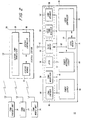
- FIG. 2 there is shown a block diagram of an exemplary TDMA communication system 22 that includes a plurality of portable TDMA transceiver units 24 that communicate with each other through a central control station 26.
- the portable transceiver units and the central control station communicate with each other over one or more frequency channels that are subdivided into TDMA channels, which are time slots during which TDMA messages are communicated.
- the central station includes a central TDMA transceiver 28 that is configured to communicate the messages with the portable transceiver units in accordance with predefined RF modulation and demodulation techniques.
- a central controller 30 executes a central control program, which is stored in a central memory 32, to control the overall operation of the TDMA communication system, including the assignment of the TDMA channels and the routing of various data and control signals within the system.
- Each portable transceiver unit 24 includes a local controller 34 that, under the control of a local control program stored in a local memory 36, controls the overall operation of the transceiver unit, including the transmission and reception of the TDMA messages during designated TDMA channels.
- the transceiver unit includes a TDMA receiver section 38 and a TDMA transmitter section 40 that are connected to a common antenna 42 via an RX/TX switch 44, which operates under the control of the local controller to couple the antenna to the transmitter section and the receiver section during corresponding transmit and receive channels.
- the transmitter section transmits bursts of messages, and the receiver section receives the messages during a designated TDMA receive channel. Additionally, the receiver section can also be used to make control or traffic channel measurements during other channels.
- a power supply 46 such as a battery, provides a supply voltage on line 48, which can be, for example, approximately 5 volts, to operate various sections of the transceiver unit.
- the receiver section 38 includes a local TDMA receiver 50 that demodulates TDMA messages received through the antenna 42 during a corresponding receive channel.
- a TDMA decoder 52 decodes the received TDMA messages and delivers them to a user as an audio or text message.
- the transmitter section 40 includes a TDMA encoder 54 that appropriately encodes audio or text messages from the user into encoded TDMA messages and delivers them to a TDMA modulator 56.
- the modulated TDMA messages are applied to an RFPA 58 which, when energized during a corresponding TDMA transmit channel, amplifies the modulated messages and couples them, through the TX/RX switch 44, to the antenna.
- the local controller 34 In accordance with the TDMA transmit and receive channel assignments of a particular transceiver unit 24, the local controller 34 generates a supply control signal on line 60, for controlling the switching of the power supply 46 and the RFPA 58, and it generates a TX/RX switch control signal on line 62, for controlling the switching of the TX/RX switch 44 between the receiver and the transmitter sections 38 and 40.
- the TDMA transmitter section includes a power interface circuit 64 that is configured according to the present invention, to provide the switching function between the supply voltage and the RFPA 58.
- the supply control signal which is generated by the local controller 34 on line 60.
- the supply control signal is at one of two binary states: a first binary state when the power supply is disconnected from the RFPA 58, and a second binary state when the power supply is connected to the RFPA 58.
- the supply control signal has a first voltage level V 1 , e.g. zero volts, and during the subsequent second binary state, it has a second voltage level V 2 , e.g. 3.75 volts.
- each first binary state corresponds to the period when the transmitter section 40 is disabled from transmitting
- the duration of each second binary state corresponds to the period when the transmitter section is enabled to transmit TDMA messages.
- Fig. 3 depicts an example wherein the supply control signal toggles the RFPA 58 on and off at approximately a 50 % duty cycle, those skilled in the art will appreciate that this waveform is idealized for discussion purposes and that, in practice, the duty cycle will vary depending on, for example, the number of time slots per TDMA frame that a transceiver unit is transmitting, whether discontinuous transmission techniques are applied, etc.
- the power interface circuit 64 uses an n-channel MOSFET, which is turned off during the first binary state to disconnect the supply voltage from the RFPA 58 and is turned on during the second binary state to connect the supply voltage to the RFPA 58.
- the n-channel MOSFET is turned off by being biased to an off-state and is turned on by being biased placed to an on-state.
- the power interface circuit 64 biases the n-channel MOSFET to the on-state by producing a gate-to-source voltage V GS , i.e., the voltage across the gate and the source of the n-channel MOSFET, that is greater or more positive than a threshold voltage V T that corresponds to the pinch-off voltage of the MOSFET.
- V GS gate-to-source voltage
- V T threshold voltage
- the power interface circuit Conversely, to bias the n-channel MOSFET to off-state with minimum channel conductivity, the power interface circuit produces a gate-to-source voltage V GS of zero volts that is less than the threshold voltage V T . This voltage will reduce the drain current I D to a negligible value, thus, turning off the n-channel MOSFET.
- the power interface circuit takes advantage of the first voltage level (V 1 ) and the second voltage level (V 2) of the supply control signal, to provide the biasing voltages for the n-channel MOSFET. More particularly, during the second binary state, the power interface circuit uses the second voltage level V 2 to provide a gate-to-source voltage V GS that is more positive than the threshold voltage V T .
- the gate-to-source voltage V GS during the second binary state is provided by connecting a capacitor to the gate of the n-channel MOSFET.
- the capacitor which is initially charged during the first binary state, provides the more positive gate-to-source voltage V GS using the voltage level of the supply control signal during the second binary state.
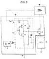
- FIG. 4 shows a schematic diagram of one exemplary embodiment of the power interface circuit 64 of the present invention.
- the power interface circuit includes an n-channel MOSFET 66 that is biased via the supply voltage, the RFPA 58, and a switch control circuit 70.
- the drain of the n-channel MOSFET 66 is coupled to the power supply, its source is coupled to the RFPA 58, and its gate is coupled to the switch control circuit 70.
- the switch control circuit In response to the supply control signal, the switch control circuit provides a gate voltage that controls the on-state and off-state of the n-channel MOSFET 66. Assuming the supply voltage provided by the power supply is 5 volts, the switch control circuit provides a gate voltage that is about 7.5 volts, i.e., V T of 2.5 volts above the battery supply voltage, which turns on the n-channel MOSFET 66.
- the switch control circuit 70 controls the switching state of the n-channel MOSFET 66 based on the binary state of the supply control signal.
- the switch control circuit uses the first voltage level V 1 during the first binary state to provide a first gate voltage that turns off the n-channel MOSFET by reducing the gate-to-source voltage V GS to zero volts, which is less than the threshold voltage V T .
- the switch control circuit uses the second voltage level V 2 to turn on the n-channel MOSFET by increasing the gate-to-source voltage V GS to a voltage level that is greater than the threshold voltage V T . In this way, the switch control circuit 70 operates the n-channel MOSFET in the on-state and off-state, in response to the voltage levels of the supply control signal during the first and second binary states.
- the switch control circuit 70 includes a complementary MOSFET pair comprising a p-channel MOSFET 72 and an n-channel MOSFET 74 that are connected to each other in series, and a capacitor 76 that is coupled across the complementary MOSFET pair.
- the p-channel MOSFET 72 and the n-channel MOSFET 74 have a common junction 78 at their drains that is connected to the gate of the n-channel MOSFET 66, to provide the gate voltage.
- the switch control circuit 70 includes a reference voltage generator 80 that generates a reference voltage V ref on line 82 substantially equal to the second voltage level V 2 , which in this example is about 3.75 volts.
- the reference voltage is provided by the power supply 46, as shown by the dotted lines.
- the reference voltage V ref may also be equal to the supply voltage.
- the reference voltage V ref is coupled to the gates of the p-channel MOSFET 72 and the n-channel MOSFET 74.
- the reference voltage V ref also couples to the source of the p-channel MOSFET 72 and to one end of the capacitor through a diode 84.
- the supply control signal on line 60 is coupled to the other end of the capacitor and to the source of the n-channel MOSFET 74, through a resistor 86.
- the p-channel and the n-channel MOSFETs 72 and 74 function in a complementary manner with respect to each other. That is, when the p-channel MOSFET 72 is on the n-channel MOSFET 74 is off, and vice versa.
- the reference voltage turns off the p-channel MOSFET 72 and turns on the n-channel MOSFET 74.
- the capacitor 76 is charged to the reference voltage level V ref . Consequently, the first voltage level V 1 of zero volts is applied as the gate voltage to the n-channel MOSFET 66, which operates the n-channel MOSFET 66 in the off-state and disconnects the power supply 46 from the RFPA 58.
- the n-channel MOSFET 74 turns off.
- the supply control signal which is coupled to the capacitor 76, produces a source voltage at the p-channel MOSFET 72 the reference voltage level V ref plus the second voltage level V 2 .
- This source voltage turns on the p-channel MOSFET 72 to connect the capacitor 76 to the gate of the n-channel MOSFET 66.
- the capacitor applies a gate voltage to the n-channel MOSFET 66 equal to the reference voltage level V ref plus the second voltage level V 2 .
- the gate voltage so produced insures a positive gate-to-source voltage of about 2.5 volts (7.5 volts gate voltage minus 5 volts supply voltage at the source) is developed, to operate the n-channel MOSFET 66 in the on-state.
- the n-channel MOSFET connects the supply voltage to the RFPA 58, which enables the transmission of the TDMA messages during the second binary state.
- the complementary MOSFETs 72 and 74 constitute a capacitor switch circuit that is responsive to the supply control signal, to control the charging of the capacitor during the first binary state and the second binary state.
- a Zener diode 73 may be coupled to the gate of the n-channel MOSFET 66 to regulate the gate voltage.
- a zener diode with 7.5- volts breakdown voltage insures that the gate-to-source voltage is greater than or equal to the threshold voltage V T , when the supply voltage is used as the reference voltage.
- the RFPA 58 is protected from voltage variations of the supply voltage. This is mainly because the voltage applied to the RFPA 58 is set by a source voltage that follows the gate voltage independent of the variations at the drain, which is coupled to the supply voltage.
- the gate voltage level is set by the reference voltage, which in one exemplary embodiment is independently generated from the supply voltage by the reference voltage generator 80.
- the reference voltage is supplied by the power supply, as in the other exemplary arrangement described above, the regulating Zener diode 73 makes the gate voltage independent of the voltage variations of the supply voltage.
- a second exemplary embodiment of the invention which operates similar to the arrangement of FIG. 4, uses a PNP bipolar transistor 90 and an NPN bipolar transistor 92, instead of the MOSFETs 72 and 74, for implementing the switch control circuit 70.
- the PNP transistor 90 is closed and the NPN 92 transistor is open, thereby charging the capacitor 76 to the voltage reference, while applying the first voltage level V 1 to the gate of the n-channel MOSFET 66.
- the n-channel MOSFET 66 is turned off, disconnecting the power supply 46 from the RFPA 58.
- the PNP transistor 90 opens.
- the gate-to-source voltage at the n-channel MOSFET turns on the n-channel MOSFET 66 and connecting the power supply to the RFPA.
- the present invention provides a simple and effective arrangement for using an n-channel MOSFET in the power interface circuit of a TDMA transmitter, thus reducing the size of such circuit and increasing its switching speed.
- the present invention takes advantage of the voltage levels provided by the supply control signal to raise the gate-to-source potential across the n-channel MOSFET to a more positive level than that provided by the power supply of the transceiver unit. In this way, the n-channel MOSFET is selectively operated in the on-state or off-state, to control the switching function between the power supply and the RFPA.
Landscapes
- Engineering & Computer Science (AREA)
- Computer Networks & Wireless Communication (AREA)
- Signal Processing (AREA)
- Power Engineering (AREA)
- Transmitters (AREA)
- Electronic Switches (AREA)
- Time-Division Multiplex Systems (AREA)
- Direct Current Feeding And Distribution (AREA)
- Transceivers (AREA)
Description
- This invention generally relates to the field of power interface circuits and, more particularly, to power interface circuits for time division multiple access (TDMA) transmitters.
- TDMA communication systems have been widely used in today's digital cellular systems, to communicate voice and data between a plurality of portable or mobile transceiver units. In such systems, a radio frequency channel is subdivided into a number of TDMA channels comprising time slots during which the transceiver units communicate TDMA messages with each other. Each transceiver unit includes a TDMA transmitter that transmits bursts of messages during an assigned transmit channel and a TDMA receiver that receives the messages during an assigned receive channel.
- In order to minimize battery current drain, a critical resource in the portable communication units, certain components of the TDMA transmitter and receiver may be energized only during their assigned channels. Moreover, even during the assigned channels, transmitter components may be turned off during periods of silence to still further reduce consumption. For example, each transmitter includes a radio frequency power amplifier (RFPA), which draws relatively significant battery current when energized. Thus, the transmitter is equipped with a power interface circuit that selectively couples the supply voltage to the RFPA only during an assigned transmit channel, to minimize battery current drain. Generally, such power interface circuit includes a switch that connects and disconnects the supply voltage to and from the RFPA under the control of a switch control signal.
- Conventionally, p-channel metal-oxide semiconductor field-effect transistors (MOSFETs) have been used as switches in the power interface circuits, for example as shown in JP 08 204796. FIG. 1 shows schematic diagram of one conventional
power interface circuit 10 that uses such p-channel MOSFET 12, which is biased throughresistors line 14 to anRFPA 16. In response to a voltage supply control signal online 18, which has two binary states, the p-channel MOSFET is turned on to connect the supply voltage to theRFPA 16 during one binary state and is turned off to disconnect the supply voltage from theRFPA 16 during another binary state. - To turn on the p-
channel MOSFET 12, a negative voltage is applied across the transistor's gate-to-source junction that increases (or enhances) the conductivity of its p-channel. Under the arrangement of FIG. 1, a negative gate voltage, i.e. ground, is applied to the p-channel MOSFET, through abipolar transistor 20, to turn on the p-channel MOSFET, and a positive gate voltage, i.e. VSUPPLY, is applied to turn it off. - Because of the desire to minimize the size and cost of portable communication units and increase their transmission speed, manufacturers are continuously searching for ways to reduce the size of the circuitry used in such units, while increasing their switching speed. Compared to p-channel MOSFETs, n-channel MOSFETs occupy two to three times less die space and provide faster switching speeds. They could also be configured to protect the RFPA from voltage peaks through simple regulation circuits, for example, by coupling a Zener diode at the gate of the MOSFET. Thus, the n-channel MOSFETs are an attractive alternative to p-channel MOSFETs in communication system switching applications.
- Despite the advantages offered by the n-channel MOSFETs, their use in portable communication units have been limited because in order to use the n-channel MOSFET as a switch, the MOSFET must be biased to operate in an on-state. Biasing the n-channel MOSFET in the on-state requires application of a gate voltage that is more positive than the supply voltage; a task not easily achievable-given the supply voltage is the highest voltage available in the communication unit.
- Thus, there exists a need for a power interface circuit that can bias an n-channel MOSFET to provide selective switching between the supply voltage and the RFPA of a TDMA transmitter. The present invention addresses this need.
- The present invention that addresses this need is embodied in a power interface circuit that uses an n-channel MOSFET, to control the application of a supply voltage as provided by a power supply to a TDMA power amplifier. In response to a switch control signal, a switch control circuit controls the n-channel MOSFET to connect or disconnect the power supply to and from the TDMA power amplifier. The switch control signal has a first binary state during which the switch control signal has a first voltage level, and it has a second binary state during which the switch control signal has a second voltage level. The switch control circuit turns off the n-channel MOSFET to disconnect the power supply from the power amplifier during the first binary state, and it turns on the n-channel MOSFET to connect the power supply to the power amplifier during the second binary state.
- In one of the exemplary features of the present invention, the n-channel MOSFET has a drain coupled to the power supply and a source connected to the power amplifier. The power interface circuit uses the first and second voltage levels of the switch control signal to control the switching state of the n-channel MOSFET by controlling a gate-to-source voltage level. During the first binary state, the power interface circuit uses the first voltage level to place the n-channel MOSFET in an off-state by producing a gate-to-source voltage level that is less than a threshold voltage level corresponding to the pinch-off voltage of the MOSFET. During the second binary state, the power interface circuit uses the second voltage level to place the n-channel MOSFET in an on-state by producing a gate-to-source voltage level that is greater than the threshold voltage. Under this arrangement, the N-channel MOSFET protects the power amplifier from supply voltage fluctuations. Alternatively, a Zener diode may be coupled to the gate of the n-channel MOSFET to regulate the gate voltage, thereby protecting the power amplifier.
- According to other exemplary features of the present invention, the power interface circuit includes a capacitor that is charged during the first binary state, when the control signal, which is coupled to the gate of the n-channel MOSFET, provides the first voltage level that turns off the n-channel MOSFET. Subsequently, during the second binary state, the capacitor is connected to the gate of the n-channel MOSFET to provide the second voltage level that is equal to or greater than the threshold voltage that turns on the MOSFET. The second voltage level provided by the capacitor is substantially equal to the sum of the voltage level of the control signal during the second binary state and the voltage level to which the capacitor was charged to during the first binary state.
- According to still other exemplary features of the present invention, the power interface circuit includes a reference voltage generator that produces a reference voltage level and a capacitor switch circuit that controls the connections of the capacitor. During the first binary state, the capacitor switch circuit connects the capacitor to the reference voltage generator, which charges the capacitor to the reference voltage level. During the second binary state, the capacitor switch circuit connects the capacitor to the gate of the n-channel MOSFET. The capacitor, which is coupled to the supply control signal, provides a gate voltage level that is substantially equal to the reference voltage level plus the level of control signal during the second binary state. The capacitor switch circuit includes MOSFETs in one exemplary embodiment of the invention and includes bipolar transistors in another exemplary embodiment.
- Other features and advantages of the present invention will become apparent from the following description of the preferred embodiment, taken in conjunction with the accompanying drawings, which illustrate, by way of example, the principles of the invention.
-
- FIG. 1 is a schematic diagram of a conventional power interface circuit.
- FIG. 2 is a block diagram of a TDMA communication system that advantageously uses an exemplary power interface circuit according to the present invention.
- FIG. 3 is a timing diagram of a supply control signal generated by the TDMA communication system of the FIG. 2.
- FIG. 4 is a schematic diagram of a power interface circuit according to one of the exemplary embodiments of the present invention.
- FIG. 5 is a schematic diagram of a power interface circuit according to another exemplary embodiment of the present invention.
- Those skilled in the art will appreciate that the present invention can be applied in other environments. For example, transmitters used in other systems having different access methodologies (e.g., code division multiple access (CDMA) on frequency division multiple access (FDMA)) could also be controlled in accordance with the following techniques.
- With respect to FIG. 2, there is shown a block diagram of an exemplary TDMA communication system 22 that includes a plurality of portable
TDMA transceiver units 24 that communicate with each other through acentral control station 26. The portable transceiver units and the central control station communicate with each other over one or more frequency channels that are subdivided into TDMA channels, which are time slots during which TDMA messages are communicated. The central station includes acentral TDMA transceiver 28 that is configured to communicate the messages with the portable transceiver units in accordance with predefined RF modulation and demodulation techniques. Acentral controller 30 executes a central control program, which is stored in acentral memory 32, to control the overall operation of the TDMA communication system, including the assignment of the TDMA channels and the routing of various data and control signals within the system. - Each
portable transceiver unit 24 includes alocal controller 34 that, under the control of a local control program stored in alocal memory 36, controls the overall operation of the transceiver unit, including the transmission and reception of the TDMA messages during designated TDMA channels. The transceiver unit includes aTDMA receiver section 38 and aTDMA transmitter section 40 that are connected to acommon antenna 42 via an RX/TX switch 44, which operates under the control of the local controller to couple the antenna to the transmitter section and the receiver section during corresponding transmit and receive channels. The transmitter section transmits bursts of messages, and the receiver section receives the messages during a designated TDMA receive channel. Additionally, the receiver section can also be used to make control or traffic channel measurements during other channels. Apower supply 46, such as a battery, provides a supply voltage online 48, which can be, for example, approximately 5 volts, to operate various sections of the transceiver unit. - The
receiver section 38 includes alocal TDMA receiver 50 that demodulates TDMA messages received through theantenna 42 during a corresponding receive channel. ATDMA decoder 52 decodes the received TDMA messages and delivers them to a user as an audio or text message. Thetransmitter section 40 includes aTDMA encoder 54 that appropriately encodes audio or text messages from the user into encoded TDMA messages and delivers them to aTDMA modulator 56. The modulated TDMA messages are applied to anRFPA 58 which, when energized during a corresponding TDMA transmit channel, amplifies the modulated messages and couples them, through the TX/RX switch 44, to the antenna. In accordance with the TDMA transmit and receive channel assignments of aparticular transceiver unit 24, thelocal controller 34 generates a supply control signal online 60, for controlling the switching of thepower supply 46 and theRFPA 58, and it generates a TX/RX switch control signal online 62, for controlling the switching of the TX/RX switch 44 between the receiver and thetransmitter sections power interface circuit 64 that is configured according to the present invention, to provide the switching function between the supply voltage and theRFPA 58. - With reference to FIG. 3, a diagram of the supply control signal, which is generated by the
local controller 34 online 60, is shown. At any given time, the supply control signal is at one of two binary states: a first binary state when the power supply is disconnected from theRFPA 58, and a second binary state when the power supply is connected to theRFPA 58. During the first binary state, the supply control signal has a first voltage level V1, e.g. zero volts, and during the subsequent second binary state, it has a second voltage level V2, e.g. 3.75 volts. As described above, the duration of each first binary state corresponds to the period when thetransmitter section 40 is disabled from transmitting, and the duration of each second binary state corresponds to the period when the transmitter section is enabled to transmit TDMA messages. Although Fig. 3 depicts an example wherein the supply control signal toggles theRFPA 58 on and off at approximately a 50 % duty cycle, those skilled in the art will appreciate that this waveform is idealized for discussion purposes and that, in practice, the duty cycle will vary depending on, for example, the number of time slots per TDMA frame that a transceiver unit is transmitting, whether discontinuous transmission techniques are applied, etc. - According to the present invention, the
power interface circuit 64 uses an n-channel MOSFET, which is turned off during the first binary state to disconnect the supply voltage from theRFPA 58 and is turned on during the second binary state to connect the supply voltage to theRFPA 58. The n-channel MOSFET is turned off by being biased to an off-state and is turned on by being biased placed to an on-state. - The
power interface circuit 64 biases the n-channel MOSFET to the on-state by producing a gate-to-source voltage VGS, i.e., the voltage across the gate and the source of the n-channel MOSFET, that is greater or more positive than a threshold voltage VT that corresponds to the pinch-off voltage of the MOSFET. As a result, negative charges are induced into the n-type channel increasing its conductivity and allowing drain current ID to flow, consequently, turning on the n-channel MOSFET. Under the current state of the art, the n-channel MOSFET used by the present invention requires a threshold voltage VT of about 2.5 volts, to provide maximum channel conductivity. - Conversely, to bias the n-channel MOSFET to off-state with minimum channel conductivity, the power interface circuit produces a gate-to-source voltage VGS of zero volts that is less than the threshold voltage VT. This voltage will reduce the drain current ID to a negligible value, thus, turning off the n-channel MOSFET. According to one of the exemplary features of the present invention, the power interface circuit takes advantage of the first voltage level (V1) and the second voltage level (V2) of the supply control signal, to provide the biasing voltages for the n-channel MOSFET. More particularly, during the second binary state, the power interface circuit uses the second voltage level V2 to provide a gate-to-source voltage VGS that is more positive than the threshold voltage VT. As described later in detail, the gate-to-source voltage VGS during the second binary state is provided by connecting a capacitor to the gate of the n-channel MOSFET. The capacitor, which is initially charged during the first binary state, provides the more positive gate-to-source voltage VGS using the voltage level of the supply control signal during the second binary state.
- FIG. 4 shows a schematic diagram of one exemplary embodiment of the
power interface circuit 64 of the present invention. The power interface circuit includes an n-channel MOSFET 66 that is biased via the supply voltage, theRFPA 58, and aswitch control circuit 70. The drain of the n-channel MOSFET 66 is coupled to the power supply, its source is coupled to theRFPA 58, and its gate is coupled to theswitch control circuit 70. - In response to the supply control signal, the switch control circuit provides a gate voltage that controls the on-state and off-state of the n-
channel MOSFET 66. Assuming the supply voltage provided by the power supply is 5 volts, the switch control circuit provides a gate voltage that is about 7.5 volts, i.e., VT of 2.5 volts above the battery supply voltage, which turns on the n-channel MOSFET 66. Theswitch control circuit 70 controls the switching state of the n-channel MOSFET 66 based on the binary state of the supply control signal. Using the first voltage level V1 during the first binary state, the switch control circuit provides a first gate voltage that turns off the n-channel MOSFET by reducing the gate-to-source voltage VGS to zero volts, which is less than the threshold voltage VT. Using the second voltage level V2, the switch control circuit turns on the n-channel MOSFET by increasing the gate-to-source voltage VGS to a voltage level that is greater than the threshold voltage VT. In this way, theswitch control circuit 70 operates the n-channel MOSFET in the on-state and off-state, in response to the voltage levels of the supply control signal during the first and second binary states. - As shown in FIG. 4, the
switch control circuit 70 according to this embodiment of the present invention includes a complementary MOSFET pair comprising a p-channel MOSFET 72 and an n-channel MOSFET 74 that are connected to each other in series, and acapacitor 76 that is coupled across the complementary MOSFET pair. The p-channel MOSFET 72 and the n-channel MOSFET 74 have acommon junction 78 at their drains that is connected to the gate of the n-channel MOSFET 66, to provide the gate voltage. In one exemplary embodiment, theswitch control circuit 70 includes areference voltage generator 80 that generates a reference voltage Vref online 82 substantially equal to the second voltage level V2, which in this example is about 3.75 volts. In another exemplary embodiment, the reference voltage is provided by thepower supply 46, as shown by the dotted lines. Thus, the reference voltage Vref may also be equal to the supply voltage. The reference voltage Vref is coupled to the gates of the p-channel MOSFET 72 and the n-channel MOSFET 74. The reference voltage Vref also couples to the source of the p-channel MOSFET 72 and to one end of the capacitor through adiode 84. The supply control signal online 60 is coupled to the other end of the capacitor and to the source of the n-channel MOSFET 74, through aresistor 86. Under this arrangement, the p-channel and the n-channel MOSFETs channel MOSFET 72 is on the n-channel MOSFET 74 is off, and vice versa. - During the first binary state, when the supply control signal is at the first voltage level V1 of zero volts, the reference voltage turns off the p-
channel MOSFET 72 and turns on the n-channel MOSFET 74. As a result, thecapacitor 76 is charged to the reference voltage level Vref. Consequently, the first voltage level V1 of zero volts is applied as the gate voltage to the n-channel MOSFET 66, which operates the n-channel MOSFET 66 in the off-state and disconnects thepower supply 46 from theRFPA 58. - During the second binary state, when the supply control signal rises to the second voltage level V2 of 3.75 volts, the n-
channel MOSFET 74 turns off. At the same time, the supply control signal, which is coupled to thecapacitor 76, produces a source voltage at the p-channel MOSFET 72 the reference voltage level Vref plus the second voltage level V2. This source voltage turns on the p-channel MOSFET 72 to connect thecapacitor 76 to the gate of the n-channel MOSFET 66. As a result, the capacitor applies a gate voltage to the n-channel MOSFET 66 equal to the reference voltage level Vref plus the second voltage level V2. The gate voltage so produced insures a positive gate-to-source voltage of about 2.5 volts (7.5 volts gate voltage minus 5 volts supply voltage at the source) is developed, to operate the n-channel MOSFET 66 in the on-state. When operating in the on-state, the n-channel MOSFET connects the supply voltage to theRFPA 58, which enables the transmission of the TDMA messages during the second binary state. Accordingly, thecomplementary MOSFETs - A
Zener diode 73, shown in dotted line, may be coupled to the gate of the n-channel MOSFET 66 to regulate the gate voltage. For example, a zener diode with 7.5- volts breakdown voltage insures that the gate-to-source voltage is greater than or equal to the threshold voltage VT, when the supply voltage is used as the reference voltage. It may be appreciated that under the arrangement described in FIG. 4, theRFPA 58 is protected from voltage variations of the supply voltage. This is mainly because the voltage applied to theRFPA 58 is set by a source voltage that follows the gate voltage independent of the variations at the drain, which is coupled to the supply voltage. The gate voltage level is set by the reference voltage, which in one exemplary embodiment is independently generated from the supply voltage by thereference voltage generator 80. In case the reference voltage is supplied by the power supply, as in the other exemplary arrangement described above, the regulatingZener diode 73 makes the gate voltage independent of the voltage variations of the supply voltage. - With reference to Fig. 5, a second exemplary embodiment of the invention which operates similar to the arrangement of FIG. 4, uses a PNP
bipolar transistor 90 and an NPNbipolar transistor 92, instead of theMOSFETs switch control circuit 70. During the first binary state, thePNP transistor 90 is closed and theNPN 92 transistor is open, thereby charging thecapacitor 76 to the voltage reference, while applying the first voltage level V1 to the gate of the n-channel MOSFET 66. As a result, the n-channel MOSFET 66 is turned off, disconnecting thepower supply 46 from theRFPA 58. During the second binary state when theNPN transistor 92 is closed, thePNP transistor 90 opens. As a result, the gate-to-source voltage at the n-channel MOSFET turns on the n-channel MOSFET 66 and connecting the power supply to the RFPA. - From the foregoing description it will be appreciated that the present invention provides a simple and effective arrangement for using an n-channel MOSFET in the power interface circuit of a TDMA transmitter, thus reducing the size of such circuit and increasing its switching speed. The present invention takes advantage of the voltage levels provided by the supply control signal to raise the gate-to-source potential across the n-channel MOSFET to a more positive level than that provided by the power supply of the transceiver unit. In this way, the n-channel MOSFET is selectively operated in the on-state or off-state, to control the switching function between the power supply and the RFPA.
- Although the invention has been described in detail with reference only to the presently preferred embodiment, those skilled in the art will appreciate that various modifications can be made without departing from the invention as defined by the following claims.
Claims (16)
- A power interface circuit (64) for a power amplifier (58), comprising:a power supply (46) that supplies a supply voltage to the power amplifier (58);an n-channel MOSFET (66) coupled between the power supply (46) and the power amplifier (58) that selectively connects the supply voltage to the power amplifier (58);a switch control circuit (70) that controls the n-channel MOSFET (66) in response to a supply control signal (60), the supply control signal (60) having a first binary state during which the n-channel MOSFET (66) is turned off and a second binary state during which the n-channel MOSFET (66) is turned on, wherein the supply control signal (60) produces a first gate voltage to turn off the n-channel MOSFET (66) and produces a second gate voltage to turn on the n-channel MOSFET (66); anda Zener diode (73) that is coupled to the n-channel MOSFET (66) to regulate the second gate voltage independently of the supply voltage (46).
- The power interface circuit (64) of claim 1, wherein the supply control signal (60) has a first voltage level during the first binary state and a second voltage level during the second binary state, wherein the n-channel MOSFET (66) is responsive to the first voltage level to be turned off and it is responsive to the second voltage level to be turned on.
- The power interface circuit (64) of claim 2, wherein the n-channel MOSFET (66) includes a gate-to-source junction, and wherein the first voltage level produces the first gate voltage across the gate-to-source junction of the n-channel MOSFET (66), and the second voltage level produces the second gate voltage across the gate-to-source junction of the n-channel MOSFET (66).
- The power interface circuit (64) of claim 3, wherein the switch control circuit (70) includes a capacitor (76) that applies the second gate voltage.
- The power interface circuit (64) of claim 3, wherein the first gate voltage is less than a threshold level.
- The power interface circuit (64) of claim 3, wherein the second gate voltage is greater than or equal to a threshold level.
- The power interface circuit (64) of claim 4 further including a reference voltage generator (80) that generates a reference voltage (VREF); wherein during the first binary state, the capacitor (76) is charged to the reference voltage level, and during the second binary state, the supply control signal is coupled to the n-channel MOSFET (66) through the capacitor (76).
- The power interface circuit (64) of claim 7 further including a capacitor switch circuit (84,72,74,86;84,90,92) that is responsive to the supply control signal (60), for controlling the connections of the capacitor (76) during the first binary state and the second binary state.
- The power interface circuit (64) of claim 8, wherein the capacitor switch circuit includes MOSFETs (72,74).
- The power interface circuit (64) of claim 8, wherein the capacitor switch circuit includes bipolar transistors (90,92).
- The power interface circuit (64) of claim 7, wherein the reference voltage is provided by the power supply (46), and where the Zener-diode (73) is coupled to the gate (G) of the n-channel MOSFET (66) to regulate the second gate voltage at a level that is grater than the threshold level.
- The power interface circuit (64) of claim 7, wherein the n-channel MOSFET (66) has a drain (D) coupled to the power supply (46) and a source (S) coupled to the power amplifier (58).
- A time division multiple access transmitter, comprising:a power amplifier;a power supply that supplies a voltage to the power amplifier; anda power interface circuit as defined in any one of claims 1 to 12.
- A method for selectively providing a supply voltage (46) to a power amplifier (58), characterised by the steps of:supplying a switch control signal (60) having a first binary state and a second binary state;turning off an n-channel MOSFET (66) during the first binary state, to disconnect the supply voltage (46) from the power amplifier (58); turning on the n-channel MOSFET (66) during the second binary state to connect the supply voltage (46) to the power amplifier (58); and regulating a gate voltage (G) that turns on the n-channel MOSFET (66) independently of the supply voltage (46), by using a Zener diode (73).
- The method of claim 14, wherein the switch control signal (60) has a first voltage level during the first binary state that turns off the n-channel MOSFET (66) and a second voltage level during the second binary state that turns on the n-channel MOSFET (66).
- The method of claim 14, wherein the first voltage level produces a first gate voltage across a gate-to-source junction of the n-channel MOSFET (66) that is less than a threshold level, and the second voltage level produces a second gate voltage that is grater than the threshold level.
Applications Claiming Priority (3)
| Application Number | Priority Date | Filing Date | Title |
|---|---|---|---|
| US08/819,937 US5892403A (en) | 1997-03-18 | 1997-03-18 | Power interface circuit for a TDMA transmitter |
| US819937 | 1997-03-18 | ||
| PCT/SE1998/000484 WO1998042080A1 (en) | 1997-03-18 | 1998-03-17 | Power interface circuit for a tdma transmitter |
Publications (2)
| Publication Number | Publication Date |
|---|---|
| EP0968569A1 EP0968569A1 (en) | 2000-01-05 |
| EP0968569B1 true EP0968569B1 (en) | 2006-08-09 |
Family
ID=25229487
Family Applications (1)
| Application Number | Title | Priority Date | Filing Date |
|---|---|---|---|
| EP98911325A Expired - Lifetime EP0968569B1 (en) | 1997-03-18 | 1998-03-17 | Power interface circuit for a tdma transmitter |
Country Status (11)
| Country | Link |
|---|---|
| US (1) | US5892403A (en) |
| EP (1) | EP0968569B1 (en) |
| JP (1) | JP2001515673A (en) |
| KR (1) | KR100464894B1 (en) |
| CN (1) | CN1100397C (en) |
| AU (1) | AU740807B2 (en) |
| BR (1) | BR9808274A (en) |
| EE (1) | EE9900408A (en) |
| HK (1) | HK1028498A1 (en) |
| MY (1) | MY123877A (en) |
| WO (1) | WO1998042080A1 (en) |
Families Citing this family (19)
| Publication number | Priority date | Publication date | Assignee | Title |
|---|---|---|---|---|
| US6148220A (en) | 1997-04-25 | 2000-11-14 | Triquint Semiconductor, Inc. | Battery life extending technique for mobile wireless applications |
| SE9803960L (en) | 1998-11-19 | 2000-05-20 | Ericsson Telefon Ab L M | cellular phone |
| US6373340B1 (en) * | 2000-08-14 | 2002-04-16 | K. S. Waves, Ltd. | High-efficiency audio power amplifier |
| US6624702B1 (en) | 2002-04-05 | 2003-09-23 | Rf Micro Devices, Inc. | Automatic Vcc control for optimum power amplifier efficiency |
| US7010284B2 (en) | 2002-11-06 | 2006-03-07 | Triquint Semiconductor, Inc. | Wireless communications device including power detector circuit coupled to sample signal at interior node of amplifier |
| US20040072554A1 (en) * | 2002-10-15 | 2004-04-15 | Triquint Semiconductor, Inc. | Automatic-bias amplifier circuit |
| US20040070454A1 (en) * | 2002-10-15 | 2004-04-15 | Triquint Semiconductor, Inc. | Continuous bias circuit and method for an amplifier |
| US7058374B2 (en) * | 2002-10-15 | 2006-06-06 | Skyworks Solutions, Inc. | Low noise switching voltage regulator |
| US20040125759A1 (en) * | 2002-12-27 | 2004-07-01 | Yochem Donald M. | Method and mobile station for operating in accordance with a discontinuous transmission mode |
| US7177370B2 (en) * | 2003-12-17 | 2007-02-13 | Triquint Semiconductor, Inc. | Method and architecture for dual-mode linear and saturated power amplifier operation |
| FR2890258B1 (en) * | 2005-08-30 | 2007-10-12 | Thales Sa | DEVICE AND METHOD FOR AMPLIFYING IMPULSE RF SIGNALS |
| US20090072225A1 (en) * | 2007-09-18 | 2009-03-19 | Electronics And Telecommunications Research Institute | Flat panel display device having organic thin film transistor and manufacturing method thereof |
| KR100907255B1 (en) * | 2007-09-18 | 2009-07-10 | 한국전자통신연구원 | Display Device Having Organic Thin Film Transistor |
| MY150267A (en) * | 2008-08-13 | 2013-12-31 | Motorola Solutions Inc | Method and apparatus for controling output power of communication equipment |
| US8471404B2 (en) * | 2009-09-16 | 2013-06-25 | Silicon Laboratories Inc. | System and method for supporting high burst current in a current limited system |
| JP5806076B2 (en) * | 2011-10-11 | 2015-11-10 | 古野電気株式会社 | RF pulse signal generation switching circuit, RF pulse signal generation circuit, and target detection apparatus |
| KR101847678B1 (en) * | 2014-01-09 | 2018-04-10 | 주식회사 만도 | Method and apparatus for implementing protection circuit based on zener diode |
| CN105786143A (en) * | 2014-12-25 | 2016-07-20 | 鸿富锦精密工业(武汉)有限公司 | Power supply system for electronic equipment |
| US9740326B2 (en) * | 2015-03-31 | 2017-08-22 | Synaptics Incorporated | Sensor array with split-drive differential sensing |
Family Cites Families (5)
| Publication number | Priority date | Publication date | Assignee | Title |
|---|---|---|---|---|
| US5111084A (en) * | 1990-05-31 | 1992-05-05 | Westinghouse Electric Corp. | Low loss drain pulser circuit for solid state microwave power amplifiers |
| JPH06261386A (en) * | 1993-03-05 | 1994-09-16 | Pioneer Electron Corp | Muting control circuit |
| US5423078A (en) * | 1993-03-18 | 1995-06-06 | Ericsson Ge Mobile Communications Inc. | Dual mode power amplifier for analog and digital cellular telephones |
| JPH08204796A (en) * | 1995-01-24 | 1996-08-09 | Oki Electric Ind Co Ltd | Power supply control circuit for radio equipment |
| US5514995A (en) * | 1995-01-30 | 1996-05-07 | Micrel, Inc. | PCMCIA power interface |
-
1997
- 1997-03-18 US US08/819,937 patent/US5892403A/en not_active Expired - Lifetime
-
1998
- 1998-03-10 MY MYPI98001033A patent/MY123877A/en unknown
- 1998-03-17 WO PCT/SE1998/000484 patent/WO1998042080A1/en active IP Right Grant
- 1998-03-17 CN CN98805240A patent/CN1100397C/en not_active Expired - Fee Related
- 1998-03-17 KR KR10-1999-7008527A patent/KR100464894B1/en not_active IP Right Cessation
- 1998-03-17 AU AU65301/98A patent/AU740807B2/en not_active Ceased
- 1998-03-17 EE EEP199900408A patent/EE9900408A/en unknown
- 1998-03-17 JP JP54044398A patent/JP2001515673A/en not_active Ceased
- 1998-03-17 EP EP98911325A patent/EP0968569B1/en not_active Expired - Lifetime
- 1998-03-17 BR BR9808274-4A patent/BR9808274A/en not_active IP Right Cessation
-
2000
- 2000-11-30 HK HK00107692A patent/HK1028498A1/en not_active IP Right Cessation
Also Published As
| Publication number | Publication date |
|---|---|
| CN1257622A (en) | 2000-06-21 |
| US5892403A (en) | 1999-04-06 |
| CN1100397C (en) | 2003-01-29 |
| KR100464894B1 (en) | 2005-01-05 |
| HK1028498A1 (en) | 2001-02-16 |
| AU6530198A (en) | 1998-10-12 |
| MY123877A (en) | 2006-06-30 |
| AU740807B2 (en) | 2001-11-15 |
| WO1998042080A1 (en) | 1998-09-24 |
| JP2001515673A (en) | 2001-09-18 |
| EP0968569A1 (en) | 2000-01-05 |
| KR20000076423A (en) | 2000-12-26 |
| EE9900408A (en) | 2000-04-17 |
| BR9808274A (en) | 2000-05-16 |
Similar Documents
| Publication | Publication Date | Title |
|---|---|---|
| EP0968569B1 (en) | Power interface circuit for a tdma transmitter | |
| US9660848B2 (en) | Methods and structures to generate on/off keyed carrier signals for signal isolators | |
| KR101902900B1 (en) | Power path switching in an electronic device including a plurality of charging ports | |
| US5689818A (en) | Mobile terminal device for telecommunications, including a switch circuit | |
| EP1698093A2 (en) | Rf backscatter transmission with zero dc power consumption | |
| US6072995A (en) | Flexible current control in power amplifiers | |
| US7529536B2 (en) | RF-controlled power saving communication system | |
| US6756843B2 (en) | Signal transmitter with pulse-controlled amplification | |
| EP0700165B1 (en) | Portable transceiver | |
| CA2019266A1 (en) | Burst mode transmitter/receiver unit | |
| US6343222B1 (en) | Dual mode power controllers and related method and radiotelephones | |
| US7116566B2 (en) | Method and circuit for controlling switching frequency signal | |
| KR19990087501A (en) | Voltage Regulator Integrated Circuits Useful for High Voltage Electronic Encoders | |
| EP1161800B1 (en) | A portable radio transceiver | |
| US5825160A (en) | Power control circuit in wireless mobile communication system | |
| KR100279374B1 (en) | Power supply circuit of wireless modem | |
| EP0225644B1 (en) | Power supply switch circuit for use in a transceiver or the like | |
| KR19990051189A (en) | Power supply voltage drop prevention device in mobile terminal | |
| AU2003201127A1 (en) | High-frequency signal switching | |
| KR100435555B1 (en) | Transceiver for half duplex communication, particularly concerned with discriminating power of a transmitter from power of a receiver when applying the power | |
| KR100323075B1 (en) | RF communication Device of low power | |
| KR940013271A (en) | Transmission output limiting circuit and method | |
| KR20010004497A (en) | Apparatus for controlling of power amplifier in portable wireless telephone set | |
| JPS6231225A (en) | Portable type radio transmitter/receiver |
Legal Events
| Date | Code | Title | Description |
|---|---|---|---|
| PUAI | Public reference made under article 153(3) epc to a published international application that has entered the european phase |
Free format text: ORIGINAL CODE: 0009012 |
|
| 17P | Request for examination filed |
Effective date: 19991018 |
|
| AK | Designated contracting states |
Kind code of ref document: A1 Designated state(s): ES GB IT SE |
|
| 17Q | First examination report despatched |
Effective date: 20040303 |
|
| RAP1 | Party data changed (applicant data changed or rights of an application transferred) |
Owner name: TELEFONAKTIEBOLAGET LM ERICSSON (PUBL) |
|
| GRAP | Despatch of communication of intention to grant a patent |
Free format text: ORIGINAL CODE: EPIDOSNIGR1 |
|
| GRAS | Grant fee paid |
Free format text: ORIGINAL CODE: EPIDOSNIGR3 |
|
| GRAA | (expected) grant |
Free format text: ORIGINAL CODE: 0009210 |
|
| AK | Designated contracting states |
Kind code of ref document: B1 Designated state(s): ES GB IT SE |
|
| PG25 | Lapsed in a contracting state [announced via postgrant information from national office to epo] |
Ref country code: IT Free format text: LAPSE BECAUSE OF FAILURE TO SUBMIT A TRANSLATION OF THE DESCRIPTION OR TO PAY THE FEE WITHIN THE PRESCRIBED TIME-LIMIT;WARNING: LAPSES OF ITALIAN PATENTS WITH EFFECTIVE DATE BEFORE 2007 MAY HAVE OCCURRED AT ANY TIME BEFORE 2007. THE CORRECT EFFECTIVE DATE MAY BE DIFFERENT FROM THE ONE RECORDED. Effective date: 20060809 |
|
| REG | Reference to a national code |
Ref country code: GB Ref legal event code: FG4D |
|
| PG25 | Lapsed in a contracting state [announced via postgrant information from national office to epo] |
Ref country code: SE Free format text: LAPSE BECAUSE OF FAILURE TO SUBMIT A TRANSLATION OF THE DESCRIPTION OR TO PAY THE FEE WITHIN THE PRESCRIBED TIME-LIMIT Effective date: 20061109 |
|
| PG25 | Lapsed in a contracting state [announced via postgrant information from national office to epo] |
Ref country code: ES Free format text: LAPSE BECAUSE OF FAILURE TO SUBMIT A TRANSLATION OF THE DESCRIPTION OR TO PAY THE FEE WITHIN THE PRESCRIBED TIME-LIMIT Effective date: 20061120 |
|
| PLBE | No opposition filed within time limit |
Free format text: ORIGINAL CODE: 0009261 |
|
| STAA | Information on the status of an ep patent application or granted ep patent |
Free format text: STATUS: NO OPPOSITION FILED WITHIN TIME LIMIT |
|
| 26N | No opposition filed |
Effective date: 20070510 |
|
| GBPC | Gb: european patent ceased through non-payment of renewal fee |
Effective date: 20070317 |
|
| PG25 | Lapsed in a contracting state [announced via postgrant information from national office to epo] |
Ref country code: GB Free format text: LAPSE BECAUSE OF NON-PAYMENT OF DUE FEES Effective date: 20070317 |