EP0959571B1 - Apparatus for the homodyne reception of optical phase shift-keyed signals - Google Patents
Apparatus for the homodyne reception of optical phase shift-keyed signals Download PDFInfo
- Publication number
- EP0959571B1 EP0959571B1 EP99109840A EP99109840A EP0959571B1 EP 0959571 B1 EP0959571 B1 EP 0959571B1 EP 99109840 A EP99109840 A EP 99109840A EP 99109840 A EP99109840 A EP 99109840A EP 0959571 B1 EP0959571 B1 EP 0959571B1
- Authority
- EP
- European Patent Office
- Prior art keywords
- output
- input
- signal
- signals
- laser
- Prior art date
- Legal status (The legal status is an assumption and is not a legal conclusion. Google has not performed a legal analysis and makes no representation as to the accuracy of the status listed.)
- Expired - Lifetime
Links
Images


Classifications
-
- H—ELECTRICITY
- H04—ELECTRIC COMMUNICATION TECHNIQUE
- H04B—TRANSMISSION
- H04B10/00—Transmission systems employing electromagnetic waves other than radio-waves, e.g. infrared, visible or ultraviolet light, or employing corpuscular radiation, e.g. quantum communication
- H04B10/60—Receivers
-
- H—ELECTRICITY
- H04—ELECTRIC COMMUNICATION TECHNIQUE
- H04B—TRANSMISSION
- H04B10/00—Transmission systems employing electromagnetic waves other than radio-waves, e.g. infrared, visible or ultraviolet light, or employing corpuscular radiation, e.g. quantum communication
- H04B10/60—Receivers
- H04B10/61—Coherent receivers
- H04B10/63—Homodyne, i.e. coherent receivers where the local oscillator is locked in frequency and phase to the carrier signal
-
- H—ELECTRICITY
- H04—ELECTRIC COMMUNICATION TECHNIQUE
- H04B—TRANSMISSION
- H04B10/00—Transmission systems employing electromagnetic waves other than radio-waves, e.g. infrared, visible or ultraviolet light, or employing corpuscular radiation, e.g. quantum communication
- H04B10/60—Receivers
- H04B10/61—Coherent receivers
- H04B10/64—Heterodyne, i.e. coherent receivers where, after the opto-electronic conversion, an electrical signal at an intermediate frequency [fIF] is obtained
-
- H—ELECTRICITY
- H04—ELECTRIC COMMUNICATION TECHNIQUE
- H04L—TRANSMISSION OF DIGITAL INFORMATION, e.g. TELEGRAPHIC COMMUNICATION
- H04L27/00—Modulated-carrier systems
- H04L27/18—Phase-modulated carrier systems, i.e. using phase-shift keying
- H04L27/22—Demodulator circuits; Receiver circuits
- H04L27/227—Demodulator circuits; Receiver circuits using coherent demodulation
- H04L27/2271—Demodulator circuits; Receiver circuits using coherent demodulation wherein the carrier recovery circuit uses only the demodulated signals
- H04L27/2272—Demodulator circuits; Receiver circuits using coherent demodulation wherein the carrier recovery circuit uses only the demodulated signals using phase locked loops
Landscapes
- Engineering & Computer Science (AREA)
- Computer Networks & Wireless Communication (AREA)
- Signal Processing (AREA)
- Physics & Mathematics (AREA)
- Electromagnetism (AREA)
- Optical Communication System (AREA)
- Digital Transmission Methods That Use Modulated Carrier Waves (AREA)
Description
Die Erfindung bezieht sich auf eine Vorrichtung für den homodynen Empfang optischer
phasenumgetasteter Signale nach dem Oberbegriff des Patentanspruchs 1.The invention relates to a device for homodyne optical reception
phase-shift keyed signals according to the preamble of
Es sind verschiedene Modulationsverfahren für Digitalsignal-Systeme der Telekommunikationstechnik bekannt, die mit Phasenumtastung arbeiten, wobei die für die Demodulation notwendige Trägerrückgewinnung beispielsweise durch Vervielfachung, durch Remodulation oder mit Hilfe des Costas-Regelkreises erfolgen kann. Bei Verwendung solcher oder ähnlicher Systeme in Zusammenhang mit optischen Signalen stellt sich häufig das Problem der Phasenregelung einer lokalen Laserquelle, was relativ aufwendig ist. Ein optischer Homodynempfänger der eingangs erwähnter Art für PSK-Signale ist beispielsweise aus der EP 0 535 494 A2 bekannt. There are various modulation methods for digital signal systems in telecommunications technology known to work with phase shift keying, the one for demodulation necessary carrier recovery, for example by multiplication, by remodulation or can be done using the Costas control loop. When using such or similar systems in connection with optical signals often arises the problem of phase control of a local laser source, which is relatively complex. An optical homodyne receiver of the type mentioned at the beginning for PSK signals is for example known from EP 0 535 494 A2.
Es ist daher Aufgabe der Erfindung, eine Vorrichtung für den homodynen Empfang optischer phasenumgetasteter Signale zu schaffen, die zu einer einfacheren Phasenregelung der lokalen Laserquelle führt.It is therefore an object of the invention to provide a device for homodyne optical reception to create phase shift keyed signals that result in easier phase control the local laser source.
Diese Aufgabe wird in vorteilhafter Weise erfindungsgemäss durch eine Vorrichtung
nach Patentanspruch 1 gelöst.According to the invention, this object is advantageously achieved by a device
solved according to
Andere vorteilhafte Ausführungen der Erfindung ergeben sich aus den weiteren abhängigen Ansprüchen.Other advantageous embodiments of the invention result from the further dependent ones Claims.
Die Erfindung wird nachfolgend beispielsweise an Hand einer Zeichnung näher erläutert.
Es zeigt:
- Fig. 1
- das Blockschaltbild eines In-Phasen-Empfängers nach der Erfindung,
- Fig. 2
- ein Zustandsdiagramm der Trägerphasen und der Spannung der empfangenen Signale in einem In-Phasen-Empfänger,
- Fig. 3
- eine schematische Darstellung eines beispielhaften Signals in einem solchen Fall,
- Fig. 4
- das Blockschaltbild eines kombinierten In-Phasen- und Quadratur-Empfän-gers nach der Erfindung,
- Fig. 5
- ein Zustandsdiagramm der Trägerphasen und der Spannung der empfangenen Signale in einem In-Phasen- und Quadratur-Empfänger,
- Fig. 6
- eine schematische Darstellung eines beispielhaften Signals in diesem Fall, und
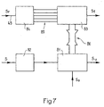
- Fig. 7
- eine schematische Darstellung einer Frequenzakquisitionsschaltung.
It shows:
- Fig. 1
- the block diagram of an in-phase receiver according to the invention,
- Fig. 2
- a state diagram of the carrier phases and the voltage of the received signals in an in-phase receiver,
- Fig. 3
- 1 shows a schematic illustration of an exemplary signal in such a case,
- Fig. 4
- the block diagram of a combined in-phase and quadrature receiver according to the invention,
- Fig. 5
- a state diagram of the carrier phases and the voltage of the received signals in an in-phase and quadrature receiver,
- Fig. 6
- is a schematic representation of an exemplary signal in this case, and
- Fig. 7
- a schematic representation of a frequency acquisition circuit.
Die erfindungsgemässe Vorrichtung 1 nach Fig. 1 umfasst einen Überlagerungsempfänger,
bestehend aus einem optischen Koppler 11, auch Hybrid genannt, und einem elektrooptischen
Wandler 12, auch Abgleichschaltung genannt, sowie einen Daten-Entscheider
2, einen Fenster-Komparator 3, auch Fenster-Diskriminator genannt, und
eine Rückkopplungseinheit 4, deren Ausgang über einen Umschalter 5, der einem Filter
6 nachgeschaltet ist, mit dem Steuereingang eines Lokal-Oszillator-Lasers 7 verbunden
ist Der die Datensignale Sd liefernde Entscheider 2 und der Komparator 3 sind eingangsseitig
an den Ausgang des Überlagerungsempfängers bzw. des E/O-Wandlers 12
angeschlossen. Die Einheit 4 wird eingangsseitig einerseits mit den vom Entscheider 2
gelieferten Datensignalen Sd und andererseits mit dem Ausgangssignal Sb des Komparators
3 beaufschlagt.The
Der optische Koppler 11 des miniaturisierten Überlagerungsempfängers weist einen Eingang
111 für einen empfangenen Lichstrahl der Frequenz fe und einen Eingang 112 für
einen von der Laserquelle 7 gelieferten Laserstrahl der Frequenz fq auf. Von den zwei
Ausgängen des Kopplers 11 liefert der eine Ausgang 113 ein optisches Summensignal
und der andere Ausgang 114 ein optisches Differenzsignal. Diese zwei optischen Signale
wirken auf je eine lichtempfindliche Diode 121 bzw. 122, die sie in entsprechende
elektrische Signale umwandeln, die in einem sich in der Schaltung 12 befindenden Verstärker
123 addiert werden, dessen Ausgang das analoge Datensignal S liefert. Der Entscheider
2 ist ein als einfacher Regenerator wirkender Nulldurchgangskomparator, der
die digitalen, das heisst rechteckförmigen Datensignale Sd abgibt.The optical coupler 11 of the miniaturized heterodyne receiver has an
Der Fenster-Komparator 3 umfasst zwei Komparatoren 31, 32, deren Signaleingänge
gemeinsam mit dem Ausgangssignal S des E/O-Wandlers 12 beaufschlagt werden, wobei
das Ausgangssignal L des Komparators 31 und das invertierte Ausgangssignal H
des Komparators 32 von einem UND-Gatter 33 verknüpft werden. In Fig. 1 sind mit L0
und H0 die Schwellenwerte der Komparatoren 31 bzw. 32 bezeichnet.The window comparator 3 comprises two
Die Rückkopplungseinheit 4 umfasst zwei UND-Gatter 41, 42, die je einen gemeinsam
mit dem Ausgang des Fenster-Komparators 3 verbundenen Eingang aufweisen. Der andere
Eingang des UND-Gatters 41 ist mit dem digitalen Datensignal Sd und der andere
Eingang des UND-Gatters 42 mit dem invertierten Datensignal Sd beaufschlagt. Die
Ausgänge der UND-Gatter 41 und 42 sind mit je einem Eingang eines Differenzverstärkers
43 verbunden, dessen Ausgang über das Filter 6 und den Umschalter 5 mit dem
Steuereingang des Lokal-Oszillator-Lasers 7 verbunden ist. Das Loop-Filter 6 kann ein
Tiefpass-Filter sein. The
Die Vorrichtung umfasst zudem eine zwischen dem Ausgang des E/O-Wandlers 12 und
dem anderen Eingang des Umschalters 5 eingefügte Frequenzakquisitionsschaltung 8,
die zudem ausgebildet ist, um den Umschalter 5 zu steuern. Für den Fenster-Komparator
3 nach Fig. 1 gilt folgende Wahrheitstabelle:
In dieser Wahrheitstabelle sind S das vom E/O-Wandler 12 gelieferte analoge Signal, Sd
das vom Entscheider 2 gewonnene Datensignal, H und L die Ausgangssignale der Komparatoren
32 bzw. 31, Sb ein vom Fenster-Komparator 3 geliefertes Synchronisationsbit
und Sv und Sw die Ausgangssignale der Gatter 41 bzw. 42. Das demodulierte Datensignal
ist allerdings mit Rauschen, Phasenfehlern und anderen Störungen behaftet.In this truth table, S is the analog signal supplied by the E /
Im Phasenkreis nach Fig. 2 beziehen sich die Referenz-Achsen auf eine Datenübertragung ohne Phasenfehler, wobei die Punkte d0 und d1 in der realen Achse Signale mit einer Phasenverschiebung von ± 90° darstellen, für die keine Auswertung der Trägerphase stattfindet. Der Punkt S in der imaginären Achse hingegen entspricht einem Signal mit einer Phasenverschiebung von 0°, bei dem eine Auswertung der Trägerphase möglich ist.In the phase circle according to FIG. 2 , the reference axes relate to data transmission without phase errors, the points d0 and d1 in the real axis representing signals with a phase shift of ± 90 ° for which no evaluation of the carrier phase takes place. The point S in the imaginary axis, however, corresponds to a signal with a phase shift of 0 °, in which an evaluation of the carrier phase is possible.
Im Phasenkreis nach Fig. 2 sind auch Punkte d0', d1' und S' dargestellt, die sich auf eine Datenübertragung mit einem Phasenfehler F beziehen, wobei die Punkte d0' und d1' Signale mit einer Phasenverschiebung von 180° darstellen, für die keine Auswertung der Trägerphase stattfindet. Der Punkt S in der Nähe des Punkts S' hingegen entspricht einem Signal mit einer erwarteten Phasenverschiebung von ungefähr 0°, bei dem eine Auswertung der Trägerphase möglich ist.In the phase circle according to FIG. 2 , points d0 ', d1' and S 'are also shown which relate to data transmission with a phase error F, the points d0' and d1 'representing signals with a phase shift of 180 °, for which none Evaluation of the carrier phase takes place. The point S near the point S ', however, corresponds to a signal with an expected phase shift of approximately 0 °, in which an evaluation of the carrier phase is possible.
In Fig. 2 unten sind die entsprechenden Spannungen der Signale d0, d0', S, S', d1' und d1 und in Fig. 3 mit punktierten geraden Linien links die untere oder niedere Grenzspannung L0 (Fig. 1) und rechts die obere oder höhere Grenzspannung H0 (Fig.1) des Fensterdiskriminators 3 angegeben. Die Empfangsspannung ist bei F > 0 positiv und bei F < 0 negativ. Dadurch kann eine Regelung der Phase F zu 0 erfolgen.In Fig. 2 below the corresponding voltages of the signals d0, d0 ', S, S', d1 'and d1 and in Fig. 3 with dotted straight lines on the left the lower or lower limit voltage L 0 ( Fig. 1 ) and on the right Upper or higher limit voltage H 0 ( Fig.1 ) of the window discriminator 3 specified. The receive voltage is positive at F> 0 and negative at F <0. This allows phase F to be regulated to 0.
Die erfindungsgemässe Vorrichtung 10 nach Fig. 4 umfasst einen In-Phasen-Überlagerungsempfänger,
einen Daten-Entscheider 20, einen Fenster-Komparator 30 und
eine gesteuerte Rückkopplungseinheit 40, deren Ausgang über einen Umschalter 50 mit
vorgeschaltetem Filter 60 an den Steuereingang eines Lokal-Oszillator-Lasers 70 angeschlossen
ist Dabei umfasst dieser Überlagerungsempfänger einen optischen Koppler
101 mit einem nachgeschalteten E/O-Wandler 102. Der die In-Phasen-Datensignale Si
liefernde Entscheider 20 und der Fenster-Komparator 30 sind eingangsseitig an den
Ausgang dieses E/O-Wandlers 102 angeschlossen. Die gesteuerte Rückkopplungseinheit
40 wird eingangsseitig einerseits mit den vom Entscheider 20 gelieferten digitalen
Datensignalen Si und andererseits mit dem Ausgangssignal des Komparators 30 beaufschlagt.The
Die Vorrichtung 10 nach Fig. 4 weist zusätzlich zwei optische Strahlteiler 13 und 14 mit
je einem Eingang 131 für das zu empfangende Licht bzw. einem Eingang 141 für das
Licht des Lokal-Oszillator-Lasers 70 sowie einen Quadratur-Überlagerungsempfänger
mit einem nachgeschalteten Daten-Entscheider 21 auf. Dieser Quadratur-Überlagerungs-empfänger
umfasst ebenfalls einen optischen Koppler 91 und einen E/O-Wandler
92, die gleich oder ähnlich wie die Elemente 101 bzw. 102 in Fig. 4 oder die
Elemente 11 bzw. 12 in Fig. 1 aufgebaut sein können. Auch die Daten-Entscheider 20
und 21 in Fig. 4 können gleich wie der Entscheider 2 in Fig. 1 aufgebaut sein. Entsprechendes
gilt für die Elemente 30, 50, 60, 70 und 80 in Fig. 4, die den Elementen 3, 5, 6,
7 bzw. 8 in Fig. 1 an sich gleich und unter sich in gleicher Weise geschaltet sein können.The
Die optischen Koppler 91 und 101 dieser miniaturisierten an sich bekannten Überlagerungsempfänger
weisen je zwei Eingänge 93 und 94 bzw. 103 und 104 auf. Die optischen
Strahiteiler 13 und 14 haben je zwei Ausgänge 133, 134 bzw. 143, 144, wobei die
Ausgänge 133 und 143 mit den Eingängen 103 bzw. 104 des Kopplers 101 des In-Phasen-Kanals
und die Ausgänge 134 und 144 mit den Eingängen 93 bzw. 94 des
Kopplers 91 des Quadratur-Kanals verbunden sind. Der Entscheider 21 ist ebenfalls ein
einfacher Regenerator, der als Nulldurchgangskomparator wirkt. Er liefert digitale Datensignale,
nämlich die Datensignale Sq des Quadraturkanals, die gemäss der Erfindung
zusätzlich dem Steuereingang der gesteuerten Rückkopplungseinheit 40 zugeführt werden.The
Die Rückkopplungseinheit 40 umfasst zwei UND-Gatter 44, 45, die je einen gemeinsam
mit dem Ausgang des Fenster-Komparators 30 verbundenen Eingang aufweisen. Der
andere Eingang des UND-Gatters 44 ist mit dem digitalen Datensignal Si und der andere
Eingang des UND-Gatters 45 mit dem invertierten Datensignal Si beaufschlagt Die Ausgänge
der UND-Gatter 44 und 45 sind mit je einem Eingang eines Modulo-2-Addierers
46 bzw. 47 verbunden, die je einen zweiten invertierenden Eingang aufweisen, die gemeinsam
mit dem Ausgang des Entscheiders 21 verbunden sind. Die Ausgänge der Addierer
46 und 47 sind mit je einem Eingang eines Differenzverstärkers 48 verbunden,
dessen Ausgang über das Filter 60 und den Umschalter 50 mit dem Steuereingang des
Lokal-Oszillator-Lasers 70 verbunden ist. Das Filter 60 ist das Loop-Filter des OPLL und
kann zum Beispiel als Tiefpass-Filter realisiert werden. Die von der Laserquelle 70 gelieferte
Strahlung wird dem Eingang 141 des Quadratur-Strahlteilers 14 zugeführt.The
Die Vorrichtung nach Fig. 4 umfasst zudem eine zwischen dem Ausgang des E/O-Wandlers
102 und dem anderen Eingang des Umschalters 50 eingefügte Frequenzakquisitionsschaltung
80, die zusätzlich den Umschalter 50 steuert. 4 also includes a
Die Schaltungen 101, 102, 20 und 30 nach Fig. 4 arbeiten genauso wie die entsprechenden
Elemente 11, 12, 2 und 3 nach Fig. 1.The
Im Phasenkreis nach Fig. 5 beziehen sich die Referenz-Achsen auf eine Datenübertragung ohne Phasenfehler, wobei die Punkte d0 und d1 in der realen Achse Signale mit einer Phasenverschiebung von ± 90° darstellen, für die keine Auswertung der Trägerphase stattfindet. Die Punkte S1 und S2 in der imaginären Achse hingegen entsprechen Signalen mit einer Phasenverschiebung von 0° bzw. 180°, bei denen eine Auswertung der Trägerphase möglich ist.5, the reference axes relate to data transmission without phase errors, with points d0 and d1 in the real axis with signals represent a phase shift of ± 90 ° for which no evaluation of the carrier phase takes place. The points S1 and S2 in the imaginary axis, however, correspond Signals with a phase shift of 0 ° or 180 °, for which an evaluation the carrier phase is possible.
Im Phasenkreis nach Fig. 2 sind auch Punkte d0', d1' und S1', S2' dargestellt, die sich auf eine Datenübertragung mit einem Phasenfehler F beziehen, wobei die Punkte d0' und d1' Signale mit einer Phasenverschiebung von ± 90° darstellen, für die keine Auswertung der Trägerphase stattfindet. Die Punkte S1' und S2' in der Nähe der Punkte S1 bzw. S2 hingegen entsprechen Signalen mit einer Phasenverschiebung von 0° bzw. 180°, beidenen eine Auswertung der Trägerphase möglich ist.Points d0 ', d1' and S1 ', S2' are also shown in the phase circle according to FIG. 2 , which relate to data transmission with a phase error F, the points d0 'and d1' representing signals with a phase shift of ± 90 ° for which there is no evaluation of the carrier phase. The points S1 'and S2' in the vicinity of the points S1 and S2, on the other hand, correspond to signals with a phase shift of 0 ° or 180 °, for which an evaluation of the carrier phase is possible.
In Fig. 5 unten sind die entsprechenden Spannungswerte der Signale d0; d0'; S2'; S1,
S2; S1'; d1'; d1 und in Fig. 6 unten mit punktierten parallelen Linien die untere Grenzspannung
L0 (Fig. 4) und die höhere Grenzspannung H0 (Fig. 4) des Fensterdiskriminators
30 für den In-Phasen-Kanal und rechts für den Quadraturkanal angegeben. Die
Empfangsspannung ist bei F > 0 positiv und bei F < 0 negativ. In Fig. 6 rechts sind die
entsprechenden Spannungswerte der Signale S1, d1, d1, S2, d0, d1, S1, d0 dargestellt.In Fig. 5 below are the corresponding voltage values of the signals d0; d0 '; S2 '; S1, S2; S1 '; d1 '; d1 and in FIG. 6 below with dotted parallel lines the lower limit voltage L 0 ( FIG. 4 ) and the higher limit voltage H 0 ( FIG. 4 ) of the
Die Frequenzakquisitionsschaltung 8 oder 80 nach Fig. 7 umfasst einen Mikroprozessor
81, an den ein Detektor 82 und eine Steuerschaltung 83 angeschlossen sind, und eine
Filterbank 84. Der Mikroprozessor 81 wird mit einem Startsignal S0 gestartet. Der an den
E/O-Wandler 12 bzw. 102 angeschlossene Detektor 82 entscheidet, ob ein echtes Signal
S vorhanden ist oder nicht, und liefert dementsprechend ein Signal 1 oder 0 an den
Mikroprozessor 81. Die Filterbank 84, die mit dem über eine Leitung 49 geführten Ausgangs-signal
Sr der Rückkopplungseinheit 4 bzw. 40 beaufschlagt wird und eine Anzahl
n Frequenzfehlerbereiche, z. B. bis 10, unterscheiden kann, liefert über einen Bus oder
Leitungen 85 entsprechende Diskriminierungssignale an die Steuerschaltung 83, die
über einen Bus 86 mit dem Mikroprozessor 81 verbunden ist, der ein Steuersignal Su für
den Umschalter 5 bzw. 50 liefert. Die Steuerschaltung 83 ihrerseits liefert ein Signal Sf,
das über den Umschalter 5 bzw. 50 dem Lokal-Oszillator-Laser 7 bzw. 70 zugeführt werden
kann.The
Die Frequenzakquisitionsschaltung 8 bzw. 80 funktioniert forlgendermassen:The
Das Eingangssignal S0 startet zunächst einen groben Frequenzsuchlauf des LO-Lasers
7 bzw. 70, der dann durch die Frequenzakquisitionsschaltung 8 bzw. 80 über den Umschalter
5 bzw. 50 auf Steuerung geschaltet wird.The input signal S0 first starts a rough frequency search of the
Wenn in einem zweiten Verfahrensschritt beim Eingang des Detektors 82 ein Signal S
festgestellt wird, das heisst, wenn der LO-Laser sich nun in der Nähe der Soll-Frequenz
befindet, wird durch den Mikroprozessor 81 die Abstimmgeschwindigkeit deutlich reduziert,
um einen Feinsuchlauf zu starten.If a signal S is detected in a second method step at the input of the
In einem dritten Verfahrensschritt wird der Frequenzfehler, das heisst, das Signal Sr auf
0 geregelt. In weiterer Ausgestaltung der Erfindung kann das Signal Sr auch über die
Leitung 49 der Frequenzakquisitionsschaltung 8 bzw. 80 zur Auswertung geführt werden.In a third method step, the frequency error, that is to say the signal Sr, is regulated to zero . In a further embodiment of the invention, the signal Sr can also be routed via
Wenn schliesslich der Mikroprozessor 81 feststellt, dass die Frequenzakquisition erreicht
wurde, schaltet die Frequenzakquisitionsschaltung 8 bzw. 80 auf Normalbetrieb und ab
diesem Moment wird der LO-Laser 7 bzw. 70 nun über das Loop-Filter 6 bzw. 60 geregelt.
Die Frequenzakquisition wird beispielsweise erreicht, wenn das Signal Sr nicht mehr
schwingt.When the
Die erwähnten Überlagerungsempfänger sind an sich bekannte miniaturisierte Bauteile
(optical hybrid + balanced receiver). Die Frequenzakquisitionsschaltung 8 bzw. 80 bewirkt,
dass die Frequenz fq des von der Laserquelle gelieferten unmodulierten Laserstrahls
geregelt wird, um eine Übereinstimmung dieser Frequenz fq mit der Frequenz fe
des empfangenen modulierten Lichtstrahls zu erreichen. Durch die Fensterdiskriminator-Schaltung
wird eine Phasenregelung der lokalen Laserquelle durchgeführt, bis ein Einrasten
der Phase erreicht wird. Bei Ausfall der Frequenzsynchronisierung wird der Umschalter
5 oder 50 wieder auf die Frequenzakquisitionsschaltung 8 bzw. 80 geschaltet.
Wenn die Frequenzsynchronisierung erreicht ist, schaltet der Umschalter nochmals auf
die Fensterdiskriminator-Schaltung um.The superimposed receivers mentioned are miniaturized components known per se (optical hybrid + balanced receiver). The
Die Arbeitsweise der erfindungsgemässen Vorrichtung ist somit weitgehend unabhängig vom angewendeten Algorithmus für die Frequenzakquisition.The mode of operation of the device according to the invention is therefore largely independent from the applied frequency acquisition algorithm.
Die Verwendung der Fensterdiskriminator-Schaltung bzw. des Fensterkomparators für den homodynen Empfang optischer phasenumgetasteter Signale ermöglicht die Bestimmung der Phase des optischen Trägersignals und damit die Phasenregelung der lokalen Laserquelle.The use of the window discriminator circuit or the window comparator for The determination enables the homodyne reception of optical phase-shift keyed signals the phase of the optical carrier signal and thus the phase control of the local Laser source.
Die Phasenregelung greift dabei auf orthogonale Trägerzustände zurück, die entweder injiziert werden, oder aber bereits, wie beim QPSK-Verfahren (Quadrature Phase Shift Keying), per se vorhanden sind. Bei der erfindungsgemässen Vorrichtung wird also der Schwellenwertentscheider des Standardempfängers um zwei oder mehrere zusätzliche Schwellen erweitert. Die Vorrichtung kann auch beim QASK-Verfahren (Quadrature Amplitude Shift Keying) oder beim BPSK-Verfahren (Binary Phase Shift Keying) mit möglichen Synchronisationssignalen verwendet werden.The phase control uses orthogonal carrier states that either injected, or already, as in the QPSK (Quadrature Phase Shift Keying), are available per se. In the device according to the invention, the Threshold decision makers of the standard receiver by two or more additional ones Thresholds expanded. The device can also be used in the QASK (Quadrature Amplitude Shift Keying) or with the BPSK process (Binary Phase Shift Keying) with possible Synchronization signals are used.
Durch die Erfindung wurde zudem die Erkenntnis gewonnen, dass die Verbindung 49
zwischen dem Ausgang der Rückkopplungseinheit 4 bzw. 40 und der Frequenzakquisitionsschaltung
8 bzw. 80 auch entfallen kann. Sie wird vorzugsweise gebraucht, wenn
die Abstimmungsgeschwindigkeit gross im Verhältnis zur Bandbreite der optischen Regelschleife
ist.The invention also gave the knowledge that the
Die durch die Eingänge 111 bzw. 131 empfangene modulierte Strahlung kann zirkular
polarisiert sein. Mit Hilfe einer vorgeschalteten λ/4-Platte kann eine Umsetzung auf eine
linear polarisierte Welle erfolgen. Am Ausgang des LO-Lasers 7 bzw. 70 können zusätzliche
Mittel zur Regelung der Polarisation eingesetzt werden.The modulated radiation received by the
Die erfindungsgemässe Vorrichtung zeichnet sich in hervorragender Weise durch eine grosse langzeitige Stabilität aus. Zudem ist ihre Realisierung sehr wenig aufwendig.The device according to the invention is outstandingly characterized by a great long-term stability. In addition, their implementation is very inexpensive.
Claims (10)
- Apparatus for the homodyne reception of phase shift-keyed signals with a heterodyne receiver (11, 12: 101, 102, 91, 92) which is provided with an input (111; 103; 93) for a light beam and an input (104; 94) for a laser signal of a local oscillator laser (7: 70), with a frequency acquisition circuit (8; 80) connected to the output of the heterodyne receiver (11, 12: 101, 102, 91, 92) and supplying signals (Sf) for the local oscillator laser (7; 70), and with a feedback unit (4; 40) for an OPLL loop inserted between the output of a data discriminator (2: 20) connected after the heterodyne receiver (11, 12; 101, 102; 91, 92) and a second input of the frequency acquisition circuit (8, 80), characterised in that a window discriminator (3; 30) the output signal (Sb) of which is used to regulate the local oscillator laser (7; 70) is inserted between the output of the heterodyne receiver (11, 12; 101,102; 91, 92) and a second input of the feedback unit (4; 40).
- Apparatus according to Claim 1, characterised in that a changeover switch (5) is provided for feeding the output signal (Sf) of the feedback unit (4) or the output signal of the frequency acquisition circuit (8) to the control input of the local oscillator laser (7).
- Apparatus according to Claim 1 or 2, characterised in that a filter circuit (6; 60) is connected before or after the changeover switch (5; 50).
- Apparatus according to Claims 1 to 3, characterised in that the feedback unit (40) has a control input connected to the output of an additional data discriminator (21) provided for a quadrature channel.
- Apparatus according to Claims 1 to 4, characterised in that at least one of these data discriminators (2; 20; 21) is a zero-crossing comparator.
- Apparatus according to Claims 1 to 5, characterised in that two optical beam splitters (13, 14) and an additional heterodyne receiver (91,92) for a quadrature channel are present, the beam splitters (13, 14) being connected to the two heterodyne receivers (101, 102, 91, 92) and the output of the local oscillator laser (70) being connected to the input of one of these beam splitters (14).
- Apparatus according to Claims 1 to 6, characterised in that the window discriminator (3; 30) has two or more thresholds.
- Apparatus according to Claims 2 to 7, characterised in that the apparatus has a detector (82) and a control circuit (83), in that the frequency acquisition circuit (8; 80) has a microprocessor (81) connected on the input side to this detector and on the output side to this control circuit (83), and in that the microprocessor (81) supplies a control signal (Su) for the changeover switch (5; 50), in that the detector is configured to decide whether or not a true signal is present at the output of an alternation converter (12; 102) of the heterodyne receiver and accordingly to supply a control signal to the microprocessor (81) and in that the control circuit (83) is configured to supply a control signal (Sf) for the local oscillator laser (7; 70) via the changeover switch (5; 50).
- Apparatus according to Claim 8, characterised in that the frequency acquisition circuit (8, 80) includes a filter circuit (84) connected on the input side to the output of the feedback unit (4, 40) and which can distinguish at least two frequency ranges, in order to supply corresponding discrimination signals to the control circuit (83).
- Apparatus according to Claims 1 to 9, characterised in that the heterodyne receiver has an optical coupler (11) with an input (111) for an incoming light beam and an input (112) for a laser beam supplied by the laser source (7), in that one output (113) of the coupler (11) supplies an optical summation signal and the other output (114) supplies an optical difference signal, and in that each of these two optical signals acts on a light-sensitive diode (121, 122) which converts them into corresponding electrical signals which are added in an amplifier (123) located in the circuit (12) the output of which amplifier (123) supplies an analog data signal (S).
Applications Claiming Priority (2)
| Application Number | Priority Date | Filing Date | Title |
|---|---|---|---|
| CH213098 | 1998-10-22 | ||
| CH213098 | 1998-10-22 |
Publications (2)
| Publication Number | Publication Date |
|---|---|
| EP0959571A1 EP0959571A1 (en) | 1999-11-24 |
| EP0959571B1 true EP0959571B1 (en) | 2001-08-29 |
Family
ID=4226587
Family Applications (1)
| Application Number | Title | Priority Date | Filing Date |
|---|---|---|---|
| EP99109840A Expired - Lifetime EP0959571B1 (en) | 1998-10-22 | 1999-05-19 | Apparatus for the homodyne reception of optical phase shift-keyed signals |
Country Status (5)
| Country | Link |
|---|---|
| US (1) | US6704375B1 (en) |
| EP (1) | EP0959571B1 (en) |
| JP (1) | JP2000134159A (en) |
| CA (1) | CA2276919A1 (en) |
| DE (1) | DE59900216D1 (en) |
Families Citing this family (9)
| Publication number | Priority date | Publication date | Assignee | Title |
|---|---|---|---|---|
| US6819879B1 (en) * | 1999-12-29 | 2004-11-16 | Nortel Networks Limited | Method and apparatus for encoding optical power and non-payload data in an optical signal |
| US7599627B2 (en) | 2001-05-31 | 2009-10-06 | Teradvance Communications, Llc | Method and system for a polarization mode dispersion tolerant optical homodyne detection system with optimized transmission modulation |
| US20040208646A1 (en) * | 2002-01-18 | 2004-10-21 | Seemant Choudhary | System and method for multi-level phase modulated communication |
| CN101442364B (en) * | 2007-11-19 | 2011-10-19 | 富士通株式会社 | Light coherent receiver, frequency difference estimation apparatus and method for light coherent receiver |
| US8401399B2 (en) | 2009-05-28 | 2013-03-19 | Freedom Photonics, Llc. | Chip-based advanced modulation format transmitter |
| US9344196B1 (en) | 2009-05-28 | 2016-05-17 | Freedom Photonics, Llc. | Integrated interferometric optical transmitter |
| US8526823B2 (en) | 2010-09-28 | 2013-09-03 | Acacia Communications, Inc. | Reconfigurable DSP performance in optical transceivers |
| US10320152B2 (en) | 2017-03-28 | 2019-06-11 | Freedom Photonics Llc | Tunable laser |
| US11923908B2 (en) * | 2021-03-19 | 2024-03-05 | The Trustees Of The University Of Pennsylvania | Integrated coherent receiver with off PLL bandwidth demodulation |
Family Cites Families (19)
| Publication number | Priority date | Publication date | Assignee | Title |
|---|---|---|---|---|
| US4037171A (en) * | 1976-02-17 | 1977-07-19 | Bell Telephone Laboratories, Incorporated | High speed tone decoder utilizing a phase-locked loop |
| US4423390A (en) * | 1981-01-09 | 1983-12-27 | Harris Corporation | Side lock avoidance network for PSK demodulator |
| JPH0239131A (en) * | 1988-07-29 | 1990-02-08 | Hitachi Ltd | Method for stabilizing frequency interval and optical heterodyne or optical homodyne communication method |
| US5007106A (en) * | 1989-11-08 | 1991-04-09 | At&T Bell Laboratories | Optical Homodyne Receiver |
| JP3001943B2 (en) * | 1990-08-30 | 2000-01-24 | 株式会社東芝 | Polarization switching light source, optical receiver, and coherent optical transmission system |
| JPH04144320A (en) * | 1990-10-05 | 1992-05-18 | Hitachi Ltd | Homodyne optical receiver |
| DE4110138C1 (en) * | 1991-03-27 | 1992-03-05 | Deutsche Forschungsanstalt Fuer Luft- Und Raumfahrt Ev, 5300 Bonn, De | Carrier recovery for optical PSK homodyne receiver - by rotating local oscillator phase 90 deg. for one synchronisation bit period to produce phase error signal |
| JP2798526B2 (en) * | 1991-06-20 | 1998-09-17 | 富士通株式会社 | Frequency discriminator |
| DE69200654T2 (en) * | 1991-08-30 | 1995-05-24 | Philips Nv | Tunable laser oscillator. |
| GB2260046B (en) * | 1991-09-26 | 1995-02-15 | Northern Telecom Ltd | Optical communications systems |
| EP0535494A3 (en) * | 1991-10-01 | 1993-09-22 | Siemens Aktiengesellschaft | Optical homodyne receiver for psk signals |
| GB2264834A (en) * | 1992-02-25 | 1993-09-08 | Northern Telecom Ltd | Optical transmission system |
| JPH077390A (en) * | 1993-06-18 | 1995-01-10 | Uniden Corp | High speed scan radio receiver and search/scan erroneous stop preventing method |
| DE4331882A1 (en) * | 1993-09-20 | 1995-03-23 | Siemens Ag | Method for operating optical heterodyne receivers with a control device which has a capture range to regulate an intermediate frequency of the receiver at an ideal value and a receiver to carry out a method of this type |
| JP3231545B2 (en) * | 1994-06-28 | 2001-11-26 | 富士通株式会社 | Optical frequency stabilizer |
| JP3866283B2 (en) * | 1994-09-14 | 2007-01-10 | コーニンクレッカ フィリップス エレクトロニクス エヌ ヴィ | Wireless transmission system and wireless device used in this system |
| US5657307A (en) * | 1995-03-10 | 1997-08-12 | Sharp Kabushiki Kaisha | Optical data reading apparatus and method |
| DE19514386A1 (en) * | 1995-04-19 | 1996-10-24 | Hertz Inst Heinrich | Optical frequency generator |
| US5687261A (en) * | 1996-01-24 | 1997-11-11 | California Institute Of Technology | Fiber-optic delay-line stabilization of heterodyne optical signal generator and method using same |
-
1999
- 1999-05-19 DE DE59900216T patent/DE59900216D1/en not_active Expired - Lifetime
- 1999-05-19 EP EP99109840A patent/EP0959571B1/en not_active Expired - Lifetime
- 1999-07-06 CA CA002276919A patent/CA2276919A1/en not_active Abandoned
- 1999-07-14 JP JP11200296A patent/JP2000134159A/en active Pending
- 1999-07-28 US US09/363,301 patent/US6704375B1/en not_active Expired - Fee Related
Also Published As
| Publication number | Publication date |
|---|---|
| US6704375B1 (en) | 2004-03-09 |
| JP2000134159A (en) | 2000-05-12 |
| EP0959571A1 (en) | 1999-11-24 |
| DE59900216D1 (en) | 2001-10-04 |
| CA2276919A1 (en) | 2000-04-22 |
Similar Documents
| Publication | Publication Date | Title |
|---|---|---|
| DE602005006231T2 (en) | Method and apparatus for the coherent demodulation of BPSK (binary phase-shift modulation) signals | |
| DE3111729C2 (en) | ||
| DE10114779A1 (en) | Sending and receiving unit | |
| EP1540858A1 (en) | Method for the transmission of optical polarization multiplex signals | |
| DE2359465A1 (en) | DIVERSITY RECEPTION SYSTEM | |
| DE3243464A1 (en) | METHOD FOR COHERENTLY DETECTING AND DEMODULATING A PHASE-MODULATED CARRIER WAVE IN ANY POLARIZATION CONDITION, AND DEVICE FOR CARRYING OUT THE METHOD | |
| EP0959571B1 (en) | Apparatus for the homodyne reception of optical phase shift-keyed signals | |
| DE2749434A1 (en) | ZERO CONTROL DEVICE FOR A MULTIPLE ANTENNA AREA | |
| DE3739484C2 (en) | ||
| DE3902826C2 (en) | ||
| DE4191618B4 (en) | Programmable digital frequency-phase discriminator | |
| DE10025237B4 (en) | Method and device for simultaneous synchronization and improved automatic frequency tracking in a communication device | |
| DE69736892T2 (en) | Non-coherent direct conversion receiver with six-gate circuit | |
| DE4331882A1 (en) | Method for operating optical heterodyne receivers with a control device which has a capture range to regulate an intermediate frequency of the receiver at an ideal value and a receiver to carry out a method of this type | |
| DE2913172B2 (en) | Receiver for high-frequency electromagnetic oscillations with frequency readjustment | |
| DE69927957T2 (en) | Demodulator with rotation means for frequency offset correction | |
| DE3216088A1 (en) | DEVICE FOR DETECTING SIGNALS INCLUDING AT LEAST ONE FIRST AND SECOND SIGNALS MODULATED ON A CARRIER SHAFT | |
| DE69736756T2 (en) | Correction of phase noise of a PLL in a PSK or QAM receiver | |
| DE69835101T2 (en) | Digital demodulator | |
| EP0065763A2 (en) | Arrangement for the fast detection of frequency-shift keying signals in a radio link | |
| DE4103687C2 (en) | Phase locked loop for demodulation | |
| DE3718103C2 (en) | ||
| DE2905331A1 (en) | Radio receiver for amplitude modulated signals - uses phase locked local oscillator and near zero intermediate frequency | |
| EP1083717B1 (en) | Phase control of a local oscillator in a coherent, optical, homodyne receiver for PSK signals | |
| DE2051879A1 (en) | Receiver for impulses modulated to a Tragerfre frequency and lying in a certain signal band |
Legal Events
| Date | Code | Title | Description |
|---|---|---|---|
| PUAI | Public reference made under article 153(3) epc to a published international application that has entered the european phase |
Free format text: ORIGINAL CODE: 0009012 |
|
| AK | Designated contracting states |
Kind code of ref document: A1 Designated state(s): BE CH DE FR GB IT LI SE |
|
| AX | Request for extension of the european patent |
Free format text: AL;LT;LV;MK;RO;SI |
|
| 17P | Request for examination filed |
Effective date: 19991013 |
|
| 17Q | First examination report despatched |
Effective date: 20000117 |
|
| RAP1 | Party data changed (applicant data changed or rights of an application transferred) |
Owner name: CONTRAVES SPACE AG |
|
| AKX | Designation fees paid |
Free format text: BE CH DE FR GB IT LI SE |
|
| GRAG | Despatch of communication of intention to grant |
Free format text: ORIGINAL CODE: EPIDOS AGRA |
|
| GRAG | Despatch of communication of intention to grant |
Free format text: ORIGINAL CODE: EPIDOS AGRA |
|
| GRAH | Despatch of communication of intention to grant a patent |
Free format text: ORIGINAL CODE: EPIDOS IGRA |
|
| GRAH | Despatch of communication of intention to grant a patent |
Free format text: ORIGINAL CODE: EPIDOS IGRA |
|
| GRAA | (expected) grant |
Free format text: ORIGINAL CODE: 0009210 |
|
| AK | Designated contracting states |
Kind code of ref document: B1 Designated state(s): BE CH DE FR GB IT LI SE |
|
| REG | Reference to a national code |
Ref country code: CH Ref legal event code: EP |
|
| REF | Corresponds to: |
Ref document number: 59900216 Country of ref document: DE Date of ref document: 20011004 |
|
| REG | Reference to a national code |
Ref country code: CH Ref legal event code: NV Representative=s name: OK PAT AG PATENTE MARKEN LIZENZEN |
|
| GBT | Gb: translation of ep patent filed (gb section 77(6)(a)/1977) |
Effective date: 20011117 |
|
| ET | Fr: translation filed | ||
| REG | Reference to a national code |
Ref country code: GB Ref legal event code: IF02 |
|
| PG25 | Lapsed in a contracting state [announced via postgrant information from national office to epo] |
Ref country code: SE Free format text: LAPSE BECAUSE OF NON-PAYMENT OF DUE FEES Effective date: 20020520 |
|
| PGFP | Annual fee paid to national office [announced via postgrant information from national office to epo] |
Ref country code: BE Payment date: 20020527 Year of fee payment: 4 |
|
| PLBE | No opposition filed within time limit |
Free format text: ORIGINAL CODE: 0009261 |
|
| STAA | Information on the status of an ep patent application or granted ep patent |
Free format text: STATUS: NO OPPOSITION FILED WITHIN TIME LIMIT |
|
| 26N | No opposition filed | ||
| EUG | Se: european patent has lapsed | ||
| PG25 | Lapsed in a contracting state [announced via postgrant information from national office to epo] |
Ref country code: GB Free format text: LAPSE BECAUSE OF NON-PAYMENT OF DUE FEES Effective date: 20030519 |
|
| PG25 | Lapsed in a contracting state [announced via postgrant information from national office to epo] |
Ref country code: BE Free format text: LAPSE BECAUSE OF NON-PAYMENT OF DUE FEES Effective date: 20030531 |
|
| BERE | Be: lapsed |
Owner name: *CONTRAVES SPACE A.G. Effective date: 20030531 |
|
| GBPC | Gb: european patent ceased through non-payment of renewal fee |
Effective date: 20030519 |
|
| PG25 | Lapsed in a contracting state [announced via postgrant information from national office to epo] |
Ref country code: IT Free format text: LAPSE BECAUSE OF NON-PAYMENT OF DUE FEES Effective date: 20050519 |
|
| REG | Reference to a national code |
Ref country code: CH Ref legal event code: PFA Owner name: OERLIKON SPACE AG Free format text: CONTRAVES SPACE AG#SCHAFFHAUSERSTRASSE 580#8052 ZUERICH (CH) -TRANSFER TO- OERLIKON SPACE AG#SCHAFFHAUSERSTRASSE 580#8052 ZUERICH (CH) |
|
| REG | Reference to a national code |
Ref country code: FR Ref legal event code: CD |
|
| REG | Reference to a national code |
Ref country code: FR Ref legal event code: PLFP Year of fee payment: 18 |
|
| REG | Reference to a national code |
Ref country code: DE Ref legal event code: R082 Ref document number: 59900216 Country of ref document: DE Representative=s name: RACH, WERNER, DIPL.-CHEM. DR.RER.NAT., DE Ref country code: DE Ref legal event code: R081 Ref document number: 59900216 Country of ref document: DE Owner name: THALES ALENIA SPACE SCHWEIZ AG, CH Free format text: FORMER OWNER: OERLIKON SPACE AG, ZUERICH, CH Ref country code: DE Ref legal event code: R081 Ref document number: 59900216 Country of ref document: DE Owner name: OEI OPTO AG, CH Free format text: FORMER OWNER: OERLIKON SPACE AG, ZUERICH, CH |
|
| REG | Reference to a national code |
Ref country code: CH Ref legal event code: PUE Owner name: OEI OPTO AG, CH Free format text: FORMER OWNER: OERLIKON SPACE AG, CH |
|
| REG | Reference to a national code |
Ref country code: CH Ref legal event code: NV Representative=s name: TROESCH SCHEIDEGGER WERNER AG, CH |
|
| REG | Reference to a national code |
Ref country code: FR Ref legal event code: TP Owner name: RUAG SCHWEIZ AG, CH Effective date: 20170213 |
|
| REG | Reference to a national code |
Ref country code: FR Ref legal event code: PLFP Year of fee payment: 19 |
|
| PGFP | Annual fee paid to national office [announced via postgrant information from national office to epo] |
Ref country code: CH Payment date: 20170505 Year of fee payment: 19 Ref country code: DE Payment date: 20170516 Year of fee payment: 19 Ref country code: FR Payment date: 20170413 Year of fee payment: 19 |
|
| REG | Reference to a national code |
Ref country code: CH Ref legal event code: NV Representative=s name: ISLER AND PEDRAZZINI AG, CH |
|
| REG | Reference to a national code |
Ref country code: CH Ref legal event code: PFA Owner name: THALES ALENIA SPACE SCHWEIZ AG, CH Free format text: FORMER OWNER: OEI OPTO AG, CH |
|
| REG | Reference to a national code |
Ref country code: DE Ref legal event code: R082 Ref document number: 59900216 Country of ref document: DE Representative=s name: RACH, WERNER, DIPL.-CHEM. DR.RER.NAT., DE Ref country code: DE Ref legal event code: R081 Ref document number: 59900216 Country of ref document: DE Owner name: THALES ALENIA SPACE SCHWEIZ AG, CH Free format text: FORMER OWNER: OEI OPTO AG, ZUERICH, CH |
|
| REG | Reference to a national code |
Ref country code: DE Ref legal event code: R119 Ref document number: 59900216 Country of ref document: DE |
|
| REG | Reference to a national code |
Ref country code: CH Ref legal event code: PL |
|
| PG25 | Lapsed in a contracting state [announced via postgrant information from national office to epo] |
Ref country code: CH Free format text: LAPSE BECAUSE OF NON-PAYMENT OF DUE FEES Effective date: 20180531 Ref country code: LI Free format text: LAPSE BECAUSE OF NON-PAYMENT OF DUE FEES Effective date: 20180531 |
|
| PG25 | Lapsed in a contracting state [announced via postgrant information from national office to epo] |
Ref country code: FR Free format text: LAPSE BECAUSE OF NON-PAYMENT OF DUE FEES Effective date: 20180531 Ref country code: DE Free format text: LAPSE BECAUSE OF NON-PAYMENT OF DUE FEES Effective date: 20181201 |