EP0951138B1 - Method for attenuating spurious signals and receiver - Google Patents
Method for attenuating spurious signals and receiver Download PDFInfo
- Publication number
- EP0951138B1 EP0951138B1 EP99660061A EP99660061A EP0951138B1 EP 0951138 B1 EP0951138 B1 EP 0951138B1 EP 99660061 A EP99660061 A EP 99660061A EP 99660061 A EP99660061 A EP 99660061A EP 0951138 B1 EP0951138 B1 EP 0951138B1
- Authority
- EP
- European Patent Office
- Prior art keywords
- mixer
- receiver
- frequency
- currents
- transistors
- Prior art date
- Legal status (The legal status is an assumption and is not a legal conclusion. Google has not performed a legal analysis and makes no representation as to the accuracy of the status listed.)
- Expired - Lifetime
Links
Images


Classifications
-
- H—ELECTRICITY
- H03—ELECTRONIC CIRCUITRY
- H03D—DEMODULATION OR TRANSFERENCE OF MODULATION FROM ONE CARRIER TO ANOTHER
- H03D7/00—Transference of modulation from one carrier to another, e.g. frequency-changing
- H03D7/14—Balanced arrangements
- H03D7/1425—Balanced arrangements with transistors
- H03D7/1433—Balanced arrangements with transistors using bipolar transistors
-
- H—ELECTRICITY
- H03—ELECTRONIC CIRCUITRY
- H03D—DEMODULATION OR TRANSFERENCE OF MODULATION FROM ONE CARRIER TO ANOTHER
- H03D7/00—Transference of modulation from one carrier to another, e.g. frequency-changing
- H03D7/14—Balanced arrangements
- H03D7/1425—Balanced arrangements with transistors
- H03D7/145—Balanced arrangements with transistors using a combination of bipolar transistors and field-effect transistors
-
- H—ELECTRICITY
- H03—ELECTRONIC CIRCUITRY
- H03D—DEMODULATION OR TRANSFERENCE OF MODULATION FROM ONE CARRIER TO ANOTHER
- H03D7/00—Transference of modulation from one carrier to another, e.g. frequency-changing
- H03D7/14—Balanced arrangements
- H03D7/1425—Balanced arrangements with transistors
- H03D7/1458—Double balanced arrangements, i.e. where both input signals are differential
-
- H—ELECTRICITY
- H03—ELECTRONIC CIRCUITRY
- H03D—DEMODULATION OR TRANSFERENCE OF MODULATION FROM ONE CARRIER TO ANOTHER
- H03D2200/00—Indexing scheme relating to details of demodulation or transference of modulation from one carrier to another covered by H03D
- H03D2200/0001—Circuit elements of demodulators
- H03D2200/0033—Current mirrors
-
- H—ELECTRICITY
- H03—ELECTRONIC CIRCUITRY
- H03D—DEMODULATION OR TRANSFERENCE OF MODULATION FROM ONE CARRIER TO ANOTHER
- H03D2200/00—Indexing scheme relating to details of demodulation or transference of modulation from one carrier to another covered by H03D
- H03D2200/0041—Functional aspects of demodulators
- H03D2200/0043—Bias and operating point
Definitions
- the invention relates to a method for attenuating spurious signals in a receiver in which radio signals are mixed to a second frequency, e.g. to an intermediate frequency (IF) or, in the case of so-called direct conversion, straight to the baseband, i.e. 0-Hz IF, and in addition the invention relates to a receiver.
- IF intermediate frequency
- the invention thus pertains to a method defined in the preamble of claim 1 and a receiver defined in the preamble of claim 7.
- the biggest problem is usually the mixing of the received signal.
- Mixing is used for converting a high-frequency received signal down to a lower intermediate frequency. Attempts are made to attenuate in different ways the mixing results of even and odd orders which are brought about in the mixing in addition to the desired result.
- the mixing results of even orders are canceled by means of balanced or double-balanced mixer constructions. In the ideal situation, the even mixing results of two branches of a mixer cancel each other as being opposite. In practice, the attenuation caused by canceling is sufficient when the intermediate frequency is right and frequency-selective filtering is used.
- Spurious responses will also be generated in a direct-conversion receiver, the worst being modulation-frequency interference at the receiver's mixer output caused by a strong amplitude-modulated (AM) signal of another transceiver. This will appear even if the frequency of the interfering signal considerably deviated from the receiving frequency.
- These interferences are mainly caused by the second-order distortion component which contains a variable-level DC component proportional to the amplitude of the interference-causing signal.
- the variable-amplitude signal produces at the mixer output a signal which comprises a variable DC component and the frequency of which is identical with the varying of the amplitude.
- This signal is attenuated in accordance with the mixer's balance accuracy and linearity. Sufficient attenuation can be achieved e.g. by using a mixer that has a good signal amplitude tolerance. In this way even spurious signals of a large amplitude will not cause a considerable interfering signal at the mixer output.
- a mixer can be based on a Gilbert cell.
- Such a mixer has to use large currents, high operating voltages and high local oscillator level to achieve a small relative portion of interfering signal and small effect on the mixer operating points. Additionally, the balance of the incoming RF signal, balance of the amplification of the different branches of the mixer, and the balance of the local oscillator are of great importance to the attenuation of spurious signals of even orders.
- the low voltage used nowadays because of the tendency to reduce power consumption causes that not all mixer types provide sufficient attenuation of spurious signals. Tolerances of the components used in the mixers are too wide to achieve a balance good enough at low voltages.
- a prior art document US-A-5 584 066 discloses balancing the mixer of a double superheterodyne receiver by adjusting bias voltages of transistors in the mixer in order to reduce carrier leakage through the mixer.
- the method according to the invention is characterized by what is expressed in claim 1.
- the receiver according to the invention is characterized by what is expressed in claim 7.
- Preferred embodiments of the invention are described in the dependent claims.
- the invention pertains to a method for attenuating spurious signals in a mixer of a receiver in which radio signals are mixed to a second frequency which may also be the baseband frequency. Mixing is balanced by adjusting transistor base bias voltages and/or currents in those transistors of the mixer circuit that receive the local oscillator signal.
- the invention also pertains to a receiver that comprises a mixer for mixing radio signals to a second frequency, which may also be the baseband frequency, and means for attenuating spurious signals while receiving radio signals.
- the means for attenuating spurious signals comprises balance-adjusting means of mixer circuit to adjust the balance of the circuit by adjusting transistor base bias voltages and/or currents in those transistors of the mixer circuit that receive the local oscillator signal.
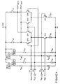
- Fig. 1 shows a known Gilbert cell used for realizing integrated IF parts such as variable gain amplifiers and mixers.
- a Gilbert cell two input voltages are multiplied into one output voltage, i.e. the voltage difference at the outputs is the product of the differences in the input voltages.
- a first voltage difference is coupled to terminals V X+ and V X- wherefrom the voltages are taken to the bases of transistors Q3, Q4 and Q6, Q7, respectively.
- a second voltage difference is coupled to terminals V Y+ and V Y- wherefrom the voltage is amplified by transistors Q5 and Q8.
- Transistors Q5 and Q8 are coupled through resistors R E1 and R E2 to a field effect transistor (FET) Q9 which is controlled by a bias voltage V BIAS and coupled to a negative operating voltage.
- Transistors Q3 and Q7 amplify a positive voltage difference V X+ and V X- , and the amplified voltage difference is coupled to outputs voltage through resistors R L1 and R L2 .
- Transistors Q2 and Q4 amplify a negative voltage difference V X+ and V X- , and the amplified voltage difference is crosscoupled to outputs V OUT+ and V OUT- .
- Fig. 2 shows in the form of flow diagram a balance adjustment method for a mixer according to the invention.
- possible previous bias voltages 1 are removed.
- the balance error 2 of the mixer is determined by coupling a radio signal to the receiver inputs, thus causing a spurious signal in the mixer, which is then measured at the mixer outputs.
- a bias voltage 3 correcting the balance error is set, preferably by feeding an inversely proportional CTRL byte corresponding to the error to the adjustment block by means of a digital controller. If the error-correcting bias voltage cannot be determined on the basis of the measurement result, a trial bias voltage is set.
- CTRL byte means a binary number that sets the control for the CTRL lines.
- the binary lines of the CTRL byte control the switching transistors in the adjustment block, so that I BIAS is changed and the voltages between the terminals of the bias resistors change.
- the potential of the operating point of the mixer's transistor input is adjusted according to the point between the bias resistors.
- the adjustment block forms a variable voltage across the resistor in the series connection when the adjustment is carried out by means of current.
- the adjustment block may also be implemented using a variable voltage source.
- the operational input signals of the transistors are alternating voltages conducted by a capacitive component. When the bias voltage that corrects or at least changes the balance error has been generated, it is checked whether the error correction was successful, i.e. whether the mixer is in balance 4.
- step 2 If not, operation returns to step 2 to determine the remaining error and change the bias voltages on the basis of that determination. If the setting of the bias reduced the balance error, the bias is increased, but if the balance error became bigger the bias is taken back towards zero or, if zero is reached, the bias is set on the second line of the input pair. Thus, bias voltage remains advantageously only on one of the lines of the input pair in the balanced state.
- the data of the balancing controller are stored in memory and normal operation of the mixer is started 5.
- Fig. 3 shows in a circuit diagram an adjustment block for the bias voltage of a mixer according to the invention.
- a current from a reference current source I REF flows via a transistor Q REF from the operating voltage VDD to ground.
- Current I REF is mirrored to a bias current circuit on the right.
- Current I BIASB through transistor Q BIASB constitutes the invariable fundamental part of bias current I BIAS .
- Transistors Q1, Q2, ... QN and Q1S, Q2S, ... QNS make up N parallel series connections, and a sum current of I 1 , I 2 , ... IN through said series connections constitutes the variable part of bias current I BIAS .
- Transistors Q1, Q2, ... QN are mutually binarily weighted such that transistors Q1S, Q2S, ... QNS, which are controlled by control lines CTRL 1, 2, ... N and connected in series with said transistors, can raise current I BIAS by 2 N -1 levels, which means the current gets 2 N values.
- Binary weighting of the currents is achieved e.g. by connecting transistors in parallel in such a way that Q1 comprises one transistor, Q2 comprises two transistors, etc. With field effect transistors (FET), the currents may also be set by selecting the channel widths.
- FET field effect transistors
- the currents are weighted preferably according to the following series: 1, 2, 4, 8, etc., i.e. 2 N , where N ⁇ 0.
- current I 1 is I REF /200
- current I 2 is I REF /100
- IN is I REF /(200/2 N-1 ).
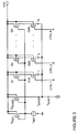
- Fig. 4 shows in a circuit diagram a mixer according to the invention.
- the blocks are for local oscillator signal pair V LO+ and V LO- and radio-frequency signal pair V RF+ and V RF- , which control through capacitive elements C1 and C2 as well as C3 and C4 the transistors Q10, Q11, Q13, Q14 and Q12, Q15.
- Blocks BLO+, BLO-, BRF+ and BRF- are used to produce currents and, thus, voltages to four parallel bias resistor series connections R B1 and R B2 , R B3 and R B4 , R B5 and R B6 as well as R B7 and R B8 .
- adjustment block current I BIAS is the same as the necessary base current of the corresponding transistor, e.g. a beta-compensated base current
- a resistor connected to ground is not used with that adjustment block. For example, if adjustment blocks BRF+ and BRF- feed the base current of transistors Q15 and Q12, resistors R B6 and R B8 are left out and the corresponding bias voltage is set by adjusting the base current.
- Load impedances Z L3 , Z L4 , transistors Q10, Q11, Q12,Q13, Q14, Q15 and emitter impedances Z E3 , Z E4 constitute a known mixer the outputs of which give signals V OUT+ and V OUT- .
- the balance is adjusted preferably as described above, but the most perfect balance is achieved by adjusting the bias voltages of the transistor pair's mutually corresponding transistors Q10, Q11 and Q13, Q14 separately.
- the controls of the transistors that get their control from the same line, such as Q10 and Q14, are separated from each other and the bias voltages of them both are adjusted individually.
- Fig. 5 shows in a circuit diagram a radio-frequency amplifier stage according to the invention which also can be used to correct a mixer's balance error.
- the blocks are for a radio-frequency signal pair V RF+ and V RF- which control through capacitive elements C5 and C6 transistors Q16 and Q17.
- Blocks BRF+ and BRF- are used to produce currents and, thus, voltages to two parallel bias resistor series connections R B9 , R B10 and R B11 , R B12 .
- Load impedances Z L5 , Z L6 , transistors Q16, Q17, emitter impedances Z E5 , Z E6 and current source I DIFF constitute a known radio-frequency amplifier stage.
- the circuit according to Fig. 5 described above can also be used as local oscillator buffer. Then the balance error of the local oscillator port can be corrected by adjusting the buffer.
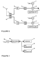
- Fig. 6 shows in the form of block diagram essential parts of a transceiver according to the invention.
- the transceiver shares a common antenna 6 from which a signal is received and filtered by a bandpass filter 7 and amplified by an amplifier 8 and refiltered 9. Then the signal at the radio reception frequency is mixed to an intermediate frequency in a balanced mixer 10 according to the invention.
- a local oscillator 11 feeds the mixer 10 at the frequency of f OSC1 .
- the balance of the mixer 10 is adjusted by a controller 12. From the intermediate frequency on the reception continues in accordance with the prior art.
- a signal to be transmitted is modulated at the local oscillator 14 frequency f OSC2 by means of a modulator 13.
- the balance of the modulator 13 is adjusted by a controller 15.
- the modulated signal is bandpass-filtered by a filter 16 and amplified by an amplifier 17 and filtered again by a filter 18 and fed to the antenna 6. Otherwise the transmitter is preferably realized according to the prior art, and this document does not take a position on the use of balancing according to the invention in it.
- Fig. 7 shows in a block diagram essential components of a controller of an adjustment block according to the invention.
- the processor 20 of a digital controller is stepped by an oscillator 19 at frequency F PRO .
- the controller executes a program from memory 21, which preferably is both read only memory (ROM) and random access memory (RAM). Measurement data on the balance is obtained by means of an A/D converter 22.
- Bias voltages are controlled by a D/A converter 23 which preferably comprises an adjustment block according to Fig. 3 in which current is switched by means of digital binary control to adjust the bias voltages.
- a radio receiver the spurious response of which is to be reduced.
- the receiver is adjusted preferably only once before use.
- a test signal is coupled to the receiver input, and the interfering signal level is measured from the receiver output.
- the test signal is generated in such a way that it produces a spurious response to be minimized.
- a trial setting is chosen e.g. for the adjustment block BRF+ of the positive line of the RF input, and the interfering signal level is measured again.
- Tuning data for the balance achieved through the minimization of spurious response are stored in the memory of the apparatus wherefrom they can be loaded by means of a microprocessor or digital signal processor (DSP) always on start-up. Fuses, microswitches, programmable gate circuits and the like can also be used for the immediate control of the adjustment block.
- DSP digital signal processor
- the selection of the bias voltage initial setting line and the level of the setting can also be realized as a preferably calculatory value based on interference measurement data.
- Empirical knowledge can also be utilized when estimating the bias voltage value on the basis of the measurement result.
- the received signal is converted digital.
- the method is advantageously applied in such a way that the spurious response is measured, adjusted as small as possible, and the settings are stored in memory by carrying out the necessary routines with a digital signal processor.
- the tuning is particularly fast as it is carried out by coupling a test signal to the antenna and executing a tuning program.
- the adjustment blocks are controlled by a microprocessor or preferably with the same digital signal processor.
- a serial or parallel bus is used for the control. For a serial bus an adjustment block needs a separate logic to control the transistors.
- the balance can also be tuned without a test signal while the local oscillator is operating.
- a comparative element is coupled to the mixer outputs to compare the voltage difference of the output pair. Particularly the DC component is compared. Tuning is performed by decreasing the voltage difference to its minimum value. However, because of bias voltages in the comparative element itself, the inputs of the comparative element must switch places and the comparison has to be repeated. The average of the tunings gives a result which is as accurate as possible. However, this tuning result is not as accurate as the one achieved using a test signal. If this type of tuning is accurate enough for the application, the tuning can be carried out automatically with a digital signal processor.
- the exemplary adjustment block was here realized by field effect transistors but the circuit can also be realized using bipolar transistors, for example.
Description
- The invention relates to a method for attenuating spurious signals in a receiver in which radio signals are mixed to a second frequency, e.g. to an intermediate frequency (IF) or, in the case of so-called direct conversion, straight to the baseband, i.e. 0-Hz IF, and in addition the invention relates to a receiver. The invention thus pertains to a method defined in the preamble of
claim 1 and a receiver defined in the preamble of claim 7. - When aiming at good linearity in radio reception, the biggest problem is usually the mixing of the received signal. Mixing is used for converting a high-frequency received signal down to a lower intermediate frequency. Attempts are made to attenuate in different ways the mixing results of even and odd orders which are brought about in the mixing in addition to the desired result. The mixing results of even orders are canceled by means of balanced or double-balanced mixer constructions. In the ideal situation, the even mixing results of two branches of a mixer cancel each other as being opposite. In practice, the attenuation caused by canceling is sufficient when the intermediate frequency is right and frequency-selective filtering is used. Then the frequencies causing the second order are attenuated already before the mixer down to a level where not too many of those frequencies will be generated in the mixer. However, there are receivers in which it is advantageous to use an intermediate frequency that might temporarily have a second-order spurious signal. Such a receiver is found e.g. in a multiple-frequency transceiver using one intermediate frequency and a common local oscillator.
- Spurious responses will also be generated in a direct-conversion receiver, the worst being modulation-frequency interference at the receiver's mixer output caused by a strong amplitude-modulated (AM) signal of another transceiver. This will appear even if the frequency of the interfering signal considerably deviated from the receiving frequency. These interferences are mainly caused by the second-order distortion component which contains a variable-level DC component proportional to the amplitude of the interference-causing signal. The variable-amplitude signal produces at the mixer output a signal which comprises a variable DC component and the frequency of which is identical with the varying of the amplitude. This signal is attenuated in accordance with the mixer's balance accuracy and linearity. Sufficient attenuation can be achieved e.g. by using a mixer that has a good signal amplitude tolerance. In this way even spurious signals of a large amplitude will not cause a considerable interfering signal at the mixer output.
- From the prior art it is known a so-called Gilbert cell which is widely used in integrated multiplier circuits of communications systems, especially in mobile communication devices. Multiplier circuits are used in integrated IF parts such as mixers and variable gain amplifiers.
- A mixer can be based on a Gilbert cell. Such a mixer has to use large currents, high operating voltages and high local oscillator level to achieve a small relative portion of interfering signal and small effect on the mixer operating points. Additionally, the balance of the incoming RF signal, balance of the amplification of the different branches of the mixer, and the balance of the local oscillator are of great importance to the attenuation of spurious signals of even orders. The low voltage used nowadays because of the tendency to reduce power consumption causes that not all mixer types provide sufficient attenuation of spurious signals. Tolerances of the components used in the mixers are too wide to achieve a balance good enough at low voltages.
- It is a problem with known radio receivers that single unbalanced mixers produce, in addition to the desired mixing result, spurious signals of both even and odd orders.
- It is another problem with known radio receivers that spurious signals of even orders, which are generated in balanced mixers in addition to the desired mixing result, are insufficiently attenuated at low voltages.
- A prior art document
US-A-5 584 066 discloses balancing the mixer of a double superheterodyne receiver by adjusting bias voltages of transistors in the mixer in order to reduce carrier leakage through the mixer. - It is an object of the invention to improve the attenuation of spurious signals of even orders so that an adequate end result will be achieved even with low operating voltages and smaller currents.
- The method according to the invention is characterized by what is expressed in
claim 1. The receiver according to the invention is characterized by what is expressed in claim 7. Preferred embodiments of the invention are described in the dependent claims. - The invention pertains to a method for attenuating spurious signals in a mixer of a receiver in which radio signals are mixed to a second frequency which may also be the baseband frequency. Mixing is balanced by adjusting transistor base bias voltages and/or currents in those transistors of the mixer circuit that receive the local oscillator signal.
- The invention also pertains to a receiver that comprises a mixer for mixing radio signals to a second frequency, which may also be the baseband frequency, and means for attenuating spurious signals while receiving radio signals. The means for attenuating spurious signals comprises balance-adjusting means of mixer circuit to adjust the balance of the circuit by adjusting transistor base bias voltages and/or currents in those transistors of the mixer circuit that receive the local oscillator signal.
- It is an advantage of the invention that in the mixing to a second frequency spurious signals of even orders caused by balance errors resulting from component tolerances are considerably attenuated.
- The invention will now be described in more detail with reference to the accompanying drawing wherein
- Fig. 1
- shows in the form of circuit diagram a known Gilbert cell,
- Fig. 2
- shows in the form of flow diagram a method according to the invention for adjusting the balance of a mixer,
- Fig. 3
- shows in the form of circuit diagram a bias voltage adjustment block of a mixer according to the invention,
- Fig. 4
- shows in the form of circuit diagram a mixer according to the invention,
- Fig. 5
- shows in the form of circuit diagram a radio-frequency stage according to the invention,
- Fig. 6
- shows in the form of block diagram essential parts of a transceiver according to the invention, and
- Fig. 7
- shows in the form of block diagram a controller according to the invention for controlling an adjustment block.
- Fig. 1 shows a known Gilbert cell used for realizing integrated IF parts such as variable gain amplifiers and mixers. In a Gilbert cell two input voltages are multiplied into one output voltage, i.e. the voltage difference at the outputs is the product of the differences in the input voltages. A first voltage difference is coupled to terminals VX+ and VX- wherefrom the voltages are taken to the bases of transistors Q3, Q4 and Q6, Q7, respectively. A second voltage difference is coupled to terminals VY+ and VY- wherefrom the voltage is amplified by transistors Q5 and Q8. Transistors Q5 and Q8 are coupled through resistors RE1 and RE2 to a field effect transistor (FET) Q9 which is controlled by a bias voltage VBIAS and coupled to a negative operating voltage. Transistors Q3 and Q7 amplify a positive voltage difference VX+ and VX-, and the amplified voltage difference is coupled to outputs voltage through resistors RL1 and RL2. Transistors Q2 and Q4 amplify a negative voltage difference VX+ and VX-, and the amplified voltage difference is crosscoupled to outputs VOUT+ and VOUT-.
- Fig. 2 shows in the form of flow diagram a balance adjustment method for a mixer according to the invention. First, possible
previous bias voltages 1 are removed. Then, thebalance error 2 of the mixer is determined by coupling a radio signal to the receiver inputs, thus causing a spurious signal in the mixer, which is then measured at the mixer outputs. Next, abias voltage 3 correcting the balance error is set, preferably by feeding an inversely proportional CTRL byte corresponding to the error to the adjustment block by means of a digital controller. If the error-correcting bias voltage cannot be determined on the basis of the measurement result, a trial bias voltage is set. CTRL byte means a binary number that sets the control for the CTRL lines. The binary lines of the CTRL byte control the switching transistors in the adjustment block, so that IBIAS is changed and the voltages between the terminals of the bias resistors change. The potential of the operating point of the mixer's transistor input is adjusted according to the point between the bias resistors. In other words, the adjustment block forms a variable voltage across the resistor in the series connection when the adjustment is carried out by means of current. The adjustment block may also be implemented using a variable voltage source. The operational input signals of the transistors are alternating voltages conducted by a capacitive component. When the bias voltage that corrects or at least changes the balance error has been generated, it is checked whether the error correction was successful, i.e. whether the mixer is in balance 4. If not, operation returns to step 2 to determine the remaining error and change the bias voltages on the basis of that determination. If the setting of the bias reduced the balance error, the bias is increased, but if the balance error became bigger the bias is taken back towards zero or, if zero is reached, the bias is set on the second line of the input pair. Thus, bias voltage remains advantageously only on one of the lines of the input pair in the balanced state. When the balancing has succeeded, the data of the balancing controller are stored in memory and normal operation of the mixer is started 5. - Fig. 3 shows in a circuit diagram an adjustment block for the bias voltage of a mixer according to the invention. In the adjustment block, a current from a reference current source IREF flows via a transistor QREF from the operating voltage VDD to ground. Current IREF is mirrored to a bias current circuit on the right. Current IBIASB through transistor QBIASB constitutes the invariable fundamental part of bias current IBIAS. Transistors Q1, Q2, ... QN and Q1S, Q2S, ... QNS make up N parallel series connections, and a sum current of I1, I2, ... IN through said series connections constitutes the variable part of bias current IBIAS.
Control lines CTRL control lines CTRL - Thus the imbalance caused by the tolerances of mixer components can be balanced using the variable part I1, I2, ... IN of current IBIAS. Also, possible small imbalance of input signals can be balanced using the arrangement according to the invention. By changing the number of control lines and the current IREF of the reference current source it is possible to adapt the bias adjustment steps and range to various couplings.
- Fig. 4 shows in a circuit diagram a mixer according to the invention. In the upper left corner of Fig. 4 there are four blocks depicted in Fig. 3 that generate the bias current IBIAS to control the bias voltage. The blocks are for local oscillator signal pair VLO+ and VLO- and radio-frequency signal pair VRF+ and VRF-, which control through capacitive elements C1 and C2 as well as C3 and C4 the transistors Q10, Q11, Q13, Q14 and Q12, Q15. Blocks BLO+, BLO-, BRF+ and BRF- are used to produce currents and, thus, voltages to four parallel bias resistor series connections RB1 and RB2, RB3 and RB4, RB5 and RB6 as well as RB7 and RB8.
- If the adjustment block current IBIAS is the same as the necessary base current of the corresponding transistor, e.g. a beta-compensated base current, a resistor connected to ground is not used with that adjustment block. For example, if adjustment blocks BRF+ and BRF- feed the base current of transistors Q15 and Q12, resistors RB6 and RB8 are left out and the corresponding bias voltage is set by adjusting the base current.
- Load impedances ZL3, ZL4, transistors Q10, Q11, Q12,Q13, Q14, Q15 and emitter impedances ZE3, ZE4 constitute a known mixer the outputs of which give signals VOUT+ and VOUT-.
- The balance is adjusted preferably as described above, but the most perfect balance is achieved by adjusting the bias voltages of the transistor pair's mutually corresponding transistors Q10, Q11 and Q13, Q14 separately. In other words, the controls of the transistors that get their control from the same line, such as Q10 and Q14, are separated from each other and the bias voltages of them both are adjusted individually.
- Fig. 5 shows in a circuit diagram a radio-frequency amplifier stage according to the invention which also can be used to correct a mixer's balance error. In the upper left corner of Fig. 5 there are two blocks depicted in Fig. 3 that generate the bias current IBIAS to control the bias voltage. The blocks are for a radio-frequency signal pair VRF+ and VRF- which control through capacitive elements C5 and C6 transistors Q16 and Q17. Blocks BRF+ and BRF- are used to produce currents and, thus, voltages to two parallel bias resistor series connections RB9, RB10 and RB11, RB12.
- Load impedances ZL5, ZL6, transistors Q16, Q17, emitter impedances ZE5, ZE6 and current source IDIFF constitute a known radio-frequency amplifier stage.
- The circuit according to Fig. 5 described above can also be used as local oscillator buffer. Then the balance error of the local oscillator port can be corrected by adjusting the buffer.
- Fig. 6 shows in the form of block diagram essential parts of a transceiver according to the invention. The transceiver shares a
common antenna 6 from which a signal is received and filtered by a bandpass filter 7 and amplified by an amplifier 8 and refiltered 9. Then the signal at the radio reception frequency is mixed to an intermediate frequency in abalanced mixer 10 according to the invention. A local oscillator 11 feeds themixer 10 at the frequency of fOSC1. The balance of themixer 10 is adjusted by acontroller 12. From the intermediate frequency on the reception continues in accordance with the prior art. - A signal to be transmitted is modulated at the
local oscillator 14 frequency fOSC2 by means of amodulator 13. The balance of themodulator 13 is adjusted by acontroller 15. The modulated signal is bandpass-filtered by afilter 16 and amplified by anamplifier 17 and filtered again by afilter 18 and fed to theantenna 6. Otherwise the transmitter is preferably realized according to the prior art, and this document does not take a position on the use of balancing according to the invention in it. - Fig. 7 shows in a block diagram essential components of a controller of an adjustment block according to the invention. The
processor 20 of a digital controller is stepped by anoscillator 19 at frequency FPRO. The controller executes a program frommemory 21, which preferably is both read only memory (ROM) and random access memory (RAM). Measurement data on the balance is obtained by means of an A/D converter 22. Bias voltages are controlled by a D/A converter 23 which preferably comprises an adjustment block according to Fig. 3 in which current is switched by means of digital binary control to adjust the bias voltages. - For example, let us consider a radio receiver the spurious response of which is to be reduced. The receiver is adjusted preferably only once before use. A test signal is coupled to the receiver input, and the interfering signal level is measured from the receiver output. The test signal is generated in such a way that it produces a spurious response to be minimized. A trial setting is chosen e.g. for the adjustment block BRF+ of the positive line of the RF input, and the interfering signal level is measured again. If the interference was reduced, an optimum setting is found for the adjustment block BRF+ by experimental bracketing, and if the interference got worse, the initial state is restored for the adjustment block BRF+ and a trial setting is chosen for the adjustment block BRF- of the negative line of the RF input and an optimum setting is found for it by experimental bracketing. The same experimental bracketing is also carried out for the local oscillator input by adjustment blocks BLO+ and BLO-. For a good result, both bracketing tunings are repeated. Thanks to the second tuning, a possible residual error, which is not noticed at the first time because it is hidden by an error in one of the input pairs, is corrected. Tuning data for the balance achieved through the minimization of spurious response are stored in the memory of the apparatus wherefrom they can be loaded by means of a microprocessor or digital signal processor (DSP) always on start-up. Fuses, microswitches, programmable gate circuits and the like can also be used for the immediate control of the adjustment block.
- Of course, the selection of the bias voltage initial setting line and the level of the setting can also be realized as a preferably calculatory value based on interference measurement data. Empirical knowledge can also be utilized when estimating the bias voltage value on the basis of the measurement result.
- In digital mobile communications devices, such as mobile stations operating in GSM, PCN (Personal Communication Network), DAMPS (Digital Advanced Mobile Phone Standard) or CDMA (Code Division Multiple Access) networks, the received signal is converted digital. In these apparatus the method is advantageously applied in such a way that the spurious response is measured, adjusted as small as possible, and the settings are stored in memory by carrying out the necessary routines with a digital signal processor. Then the tuning is particularly fast as it is carried out by coupling a test signal to the antenna and executing a tuning program. The adjustment blocks are controlled by a microprocessor or preferably with the same digital signal processor. A serial or parallel bus is used for the control. For a serial bus an adjustment block needs a separate logic to control the transistors.
- The balance can also be tuned without a test signal while the local oscillator is operating. To that end, a comparative element is coupled to the mixer outputs to compare the voltage difference of the output pair. Particularly the DC component is compared. Tuning is performed by decreasing the voltage difference to its minimum value. However, because of bias voltages in the comparative element itself, the inputs of the comparative element must switch places and the comparison has to be repeated. The average of the tunings gives a result which is as accurate as possible. However, this tuning result is not as accurate as the one achieved using a test signal. If this type of tuning is accurate enough for the application, the tuning can be carried out automatically with a digital signal processor.
- The exemplary adjustment block was here realized by field effect transistors but the circuit can also be realized using bipolar transistors, for example.
- The invention is not limited to the exemplary embodiments described above but many modifications are possible within the scope of the inventional idea defined by the claims set forth below.
Claims (13)
- A method for attenuating spurious signals in a mixer of a receiver in which radio signals of a first frequency are mixed to a second frequency, wherein the mixing is accomplished in a Gilbert cell having four upper transistors (Q10, Q11, Q13, Q14) that receive a local oscillator signal at their bases, and two lower transistors (Q12, Q15) that receive said signals of a first frequency at their bases and are coupled to said four upper transistors (Q 10, Q11, Q13, Q 14), characterized in that the mixer is balanced by adjusting bias voltages (3) and/or currents applied to the bases of selected ones of said upper transistors.
- The method of claim 1, characterized in that bias voltages and/or currents are also adjusted (3) in an input circuit that connects a local oscillator input (VLO+, VLO-) to the base of an upper transistor (Q10, Q11, Q13, Q14).
- The method of claim 1 or 2, characterized in that bias voltages and/or currents are also adjusted (3) in an input circuit that receives said signals of a first frequency and couples them to the base of a lower transistor (Q12, Q15).
- The method of claim 1, 2 or 3, characterized in that the bias voltages (3) and/or currents are adjusted separately for both transistors of a transistor pair of a signal line in the mixer circuit.
- The method of any one of the preceding claims 1 to 4, characterized in that the adjustment of the bias voltages (3) and/or currents is performed using a digital-to-analog converter that generates a bias current corresponding to a control byte fed thereto.
- The method of any one of the preceding claims 1 to 5, characterized in that the bias voltages (3) and/or currents are adjusted by measuring (2) a balance from the outputs of a receiver that includes said mixer and empirically adjusting the bias voltages (3) and/or currents on the basis of such measurements (4).
- A receiver comprising a mixer (10) for mixing radio signals of a first frequency to a second frequency, comprising:- a Gilbert cell having four upper transistors (Q10, Q11, Q 13, Q 14) with their bases coupled to local oscillator inputs of the mixer, and two lower transistors (Q12, Q 15) coupled to receive said signals of a first frequency at their bases and coupled to said four upper transistors (Q10, Q11, Q13, Q14), and- means for attenuating spurious signals,characterized in that the means for attenuating spurious signals comprises balance adjustment means (12) configured to adjust the mixer's balance by adjusting bias voltages and/or currents applied to the bases of selected ones of said upper transistors (Q10, Q11, Q 13, Q 14).
- The receiver of claim 7, characterized in that the adjustment means (12) comprises a block (BLO+, BLO-) adapted to control the bias voltage of a coupling between a local oscillator input (VLO+, VLO-) and the bases of the upper transistors coupled to that local oscillator input.
- The receiver of claim 7 or 8, characterized in that the adjustment means (12) comprises a block (BRF+, BRF-) adapted to control the bias voltage of a coupling between an input (VRF+, VRF-) configured to receive said signals of a first frequency and the base of the lower transistor coupled to that input.
- The receiver of claim 7, 8 or 9, characterized in that the adjustment means (12) comprises both a block (BLO+, BLO-) adapted to control the bias voltage of a coupling between a local oscillator input (VLO+, VLO-) and the bases of the upper transistors coupled to that local oscillator input and a block (BRF+, BRF-) adapted to control the bias voltage of a coupling between an input (VRF+, VRF-) configured to receive said signals of a first frequency and the base of the lower transistor coupled to that input.
- The receiver of any one of the preceding claims 7 to 10, characterized in that the adjustment means comprises a digital-to-analog converter (19) to adjust bias voltages and/or currents with a digital controller (12).
- The receiver of any one of the preceding claims 7 to 11, characterized in that it further comprises- an A/D converter (18) to measure the balance,- a D/A converter (19) to adjust bias voltages and/or currents, and- an oscillator (15), a processor (16) and memory (17) to carry out balance measurement routines as well as bias voltage and/or current adjustment routines.
- A mobile station comprising a receiver according to any of claims 7 to 11.
Priority Applications (2)
| Application Number | Priority Date | Filing Date | Title |
|---|---|---|---|
| EP06027107A EP1764913A3 (en) | 1998-04-17 | 1999-04-16 | Receiver for attenuating spurious signals |
| EP07008103.9A EP1811649B1 (en) | 1998-04-17 | 1999-04-16 | Method for attenuating spurious signals and receiver |
Applications Claiming Priority (2)
| Application Number | Priority Date | Filing Date | Title |
|---|---|---|---|
| FI980858 | 1998-04-17 | ||
| FI980858A FI119214B (en) | 1998-04-17 | 1998-04-17 | Method for attenuation of bias signals and receiver |
Related Child Applications (2)
| Application Number | Title | Priority Date | Filing Date |
|---|---|---|---|
| EP06027107A Division EP1764913A3 (en) | 1998-04-17 | 1999-04-16 | Receiver for attenuating spurious signals |
| EP07008103.9A Division EP1811649B1 (en) | 1998-04-17 | 1999-04-16 | Method for attenuating spurious signals and receiver |
Publications (2)
| Publication Number | Publication Date |
|---|---|
| EP0951138A1 EP0951138A1 (en) | 1999-10-20 |
| EP0951138B1 true EP0951138B1 (en) | 2007-06-20 |
Family
ID=8551535
Family Applications (3)
| Application Number | Title | Priority Date | Filing Date |
|---|---|---|---|
| EP99660061A Expired - Lifetime EP0951138B1 (en) | 1998-04-17 | 1999-04-16 | Method for attenuating spurious signals and receiver |
| EP07008103.9A Expired - Lifetime EP1811649B1 (en) | 1998-04-17 | 1999-04-16 | Method for attenuating spurious signals and receiver |
| EP06027107A Withdrawn EP1764913A3 (en) | 1998-04-17 | 1999-04-16 | Receiver for attenuating spurious signals |
Family Applications After (2)
| Application Number | Title | Priority Date | Filing Date |
|---|---|---|---|
| EP07008103.9A Expired - Lifetime EP1811649B1 (en) | 1998-04-17 | 1999-04-16 | Method for attenuating spurious signals and receiver |
| EP06027107A Withdrawn EP1764913A3 (en) | 1998-04-17 | 1999-04-16 | Receiver for attenuating spurious signals |
Country Status (3)
| Country | Link |
|---|---|
| EP (3) | EP0951138B1 (en) |
| DE (1) | DE69936324T2 (en) |
| FI (1) | FI119214B (en) |
Families Citing this family (15)
| Publication number | Priority date | Publication date | Assignee | Title |
|---|---|---|---|---|
| US6871057B2 (en) | 2000-03-08 | 2005-03-22 | Nippon Telegraph And Telephone Corporation | Mixer circuit |
| US6931083B1 (en) | 2000-05-26 | 2005-08-16 | Telasic Communications, Inc. | Low noise, low distortion, muxable Gilbert mixer signal processing system and method with AGC functionality |
| FR2814607B1 (en) * | 2000-09-26 | 2003-02-07 | St Microelectronics Sa | POLARIZATION OF A MIXER |
| US6785530B2 (en) * | 2001-03-16 | 2004-08-31 | Skyworks Solutions, Inc. | Even-order non-linearity correction feedback for Gilbert style mixers |
| WO2002084859A1 (en) | 2001-04-18 | 2002-10-24 | Nokia Corporation | Balanced circuit arrangement and method for linearizing such an arrangement |
| US6647273B2 (en) | 2001-12-28 | 2003-11-11 | Nokia Corporation | Method and apparatus for reducing power consumption in transceivers in wireless communications systems having a power control loop |
| FR2847744A1 (en) * | 2002-11-26 | 2004-05-28 | St Microelectronics Sa | Frequency transportation device second order non-linearity reducing method for wireless communication system e.g. cellular telephone, involves adjusting tension differences applied to transistor pair bases close to output voltage |
| EP1784913B1 (en) * | 2004-07-06 | 2008-05-07 | Acp Advanced Circuit Pursuit Ag | Balanced mixer using fits |
| US7356317B2 (en) * | 2004-07-14 | 2008-04-08 | Silicon Storage Technology, Inc. | Adaptive-biased mixer |
| DE102005028747B4 (en) | 2005-06-21 | 2010-12-16 | Infineon Technologies Ag | Mixer arrangement, use of the mixer arrangement and method for frequency conversion |
| US8045944B2 (en) * | 2007-09-14 | 2011-10-25 | Qualcomm Incorporated | Offset correction for passive mixers |
| EP2792064A1 (en) | 2011-12-15 | 2014-10-22 | Marvell World Trade Ltd. | Rf power detection circuit with insensitivity to process, temperature and load impedance variation |
| AU2017374750B2 (en) * | 2016-12-14 | 2022-08-04 | Bae Systems Plc | Variable frequency oscillator circuits and methods of generating an oscillating signal of a desired frequency |
| EP3349353A1 (en) * | 2017-01-12 | 2018-07-18 | BAE SYSTEMS plc | Variable frequency oscillator circuits and methods of generating an oscillating signal of a desired frequency |
| GB2557637B (en) * | 2016-12-14 | 2022-06-22 | Bae Systems Plc | Variable frequency oscillator circuits and methods of generating an oscillating signal of a desired frequency |
Family Cites Families (7)
| Publication number | Priority date | Publication date | Assignee | Title |
|---|---|---|---|---|
| US5379457A (en) * | 1993-06-28 | 1995-01-03 | Hewlett-Packard Company | Low noise active mixer |
| US5392003A (en) * | 1993-08-09 | 1995-02-21 | Motorola, Inc. | Wide tuning range operational transconductance amplifiers |
| JP3565281B2 (en) * | 1993-10-08 | 2004-09-15 | ソニー株式会社 | Receiving machine |
| ZA95605B (en) * | 1994-04-28 | 1995-12-20 | Qualcomm Inc | Method and apparatus for automatic gain control and dc offset cancellation in quadrature receiver |
| JPH0856121A (en) * | 1994-08-10 | 1996-02-27 | Advantest Corp | Frequency converter |
| US5613233A (en) * | 1994-09-30 | 1997-03-18 | Rockwell International Corp. | Apparatus with distortion cancelling feedback signal |
| US6138000A (en) * | 1995-08-21 | 2000-10-24 | Philips Electronics North America Corporation | Low voltage temperature and Vcc compensated RF mixer |
-
1998
- 1998-04-17 FI FI980858A patent/FI119214B/en active IP Right Grant
-
1999
- 1999-04-16 DE DE69936324T patent/DE69936324T2/en not_active Expired - Lifetime
- 1999-04-16 EP EP99660061A patent/EP0951138B1/en not_active Expired - Lifetime
- 1999-04-16 EP EP07008103.9A patent/EP1811649B1/en not_active Expired - Lifetime
- 1999-04-16 EP EP06027107A patent/EP1764913A3/en not_active Withdrawn
Non-Patent Citations (1)
| Title |
|---|
| None * |
Also Published As
| Publication number | Publication date |
|---|---|
| EP1811649A3 (en) | 2007-08-08 |
| DE69936324T2 (en) | 2008-02-21 |
| EP1811649A2 (en) | 2007-07-25 |
| FI980858A (en) | 1999-10-18 |
| FI980858A0 (en) | 1998-04-17 |
| EP1811649B1 (en) | 2013-09-18 |
| EP1764913A2 (en) | 2007-03-21 |
| FI119214B (en) | 2008-08-29 |
| DE69936324D1 (en) | 2007-08-02 |
| EP0951138A1 (en) | 1999-10-20 |
| EP1764913A3 (en) | 2007-04-04 |
Similar Documents
| Publication | Publication Date | Title |
|---|---|---|
| US6393260B1 (en) | Method for attenuating spurious signals and receiver | |
| EP0951138B1 (en) | Method for attenuating spurious signals and receiver | |
| US7236761B2 (en) | Balanced circuit arrangement and method for linearizing such an arrangement | |
| RU2315423C2 (en) | Distortion suppressing calibration | |
| US8411730B2 (en) | Semiconductor integrated communication circuit and operation method thereof | |
| EP1393403B1 (en) | Tunable phase shifter and applications for same | |
| AU641075B2 (en) | Apparatus and method of DC offset correction for a receiver | |
| US6366166B1 (en) | Double pass band amplifier circuit and a radio frequency reception head | |
| EP1501189B1 (en) | High frequency variable gain amplification device, control device, high frequency variable gain frequency-conversion device, and communication device | |
| EP1414163A1 (en) | Receiver and communication terminal | |
| KR100794983B1 (en) | Method and system for suppressing carrier leakage | |
| US6088581A (en) | Method and apparatus for reducing amplitude modulated interference in a receiver | |
| US6771945B1 (en) | Dynamic DC balancing of a direct conversion receiver and method | |
| US11581852B2 (en) | Systems and methods for detecting local oscillator leakage and image tone in I/Q mixer based transceivers | |
| EP1236285B1 (en) | Receiver circuit | |
| US7555272B2 (en) | Transmission arrangement for transmitting data continuously in the time domain | |
| US7272187B2 (en) | Filter circuit and radio apparatus | |
| JP2005057745A (en) | High-frequency variable gain amplifier, controller, high-frequency variable gain frequency converter, and communication device | |
| EP1652292B1 (en) | Offset correction for down-conversion mixers | |
| JPH09252324A (en) | Frequency converter |
Legal Events
| Date | Code | Title | Description |
|---|---|---|---|
| PUAI | Public reference made under article 153(3) epc to a published international application that has entered the european phase |
Free format text: ORIGINAL CODE: 0009012 |
|
| AK | Designated contracting states |
Kind code of ref document: A1 Designated state(s): DE FR GB IT |
|
| AX | Request for extension of the european patent |
Free format text: AL;LT;LV;MK;RO;SI |
|
| AKX | Designation fees paid |
Free format text: AT BE CH CY LI |
|
| 17P | Request for examination filed |
Effective date: 20000412 |
|
| RBV | Designated contracting states (corrected) |
Designated state(s): DE FR GB IT |
|
| REG | Reference to a national code |
Ref country code: DE Ref legal event code: 8566 |
|
| RAP1 | Party data changed (applicant data changed or rights of an application transferred) |
Owner name: NOKIA CORPORATION |
|
| 17Q | First examination report despatched |
Effective date: 20040802 |
|
| GRAP | Despatch of communication of intention to grant a patent |
Free format text: ORIGINAL CODE: EPIDOSNIGR1 |
|
| GRAS | Grant fee paid |
Free format text: ORIGINAL CODE: EPIDOSNIGR3 |
|
| GRAA | (expected) grant |
Free format text: ORIGINAL CODE: 0009210 |
|
| AK | Designated contracting states |
Kind code of ref document: B1 Designated state(s): DE FR GB IT |
|
| REG | Reference to a national code |
Ref country code: GB Ref legal event code: FG4D |
|
| RBV | Designated contracting states (corrected) |
Designated state(s): DE FR IT |
|
| REF | Corresponds to: |
Ref document number: 69936324 Country of ref document: DE Date of ref document: 20070802 Kind code of ref document: P |
|
| ET | Fr: translation filed | ||
| PLBE | No opposition filed within time limit |
Free format text: ORIGINAL CODE: 0009261 |
|
| STAA | Information on the status of an ep patent application or granted ep patent |
Free format text: STATUS: NO OPPOSITION FILED WITHIN TIME LIMIT |
|
| 26N | No opposition filed |
Effective date: 20080325 |
|
| REG | Reference to a national code |
Ref country code: DE Ref legal event code: R082 Ref document number: 69936324 Country of ref document: DE Representative=s name: SAMSON & PARTNER, PATENTANWAELTE, DE |
|
| REG | Reference to a national code |
Ref country code: FR Ref legal event code: TP Owner name: NOKIA TECHNOLOGIES OY, FI Effective date: 20150318 |
|
| REG | Reference to a national code |
Ref country code: DE Ref legal event code: R082 Ref document number: 69936324 Country of ref document: DE Representative=s name: SAMSON & PARTNER PATENTANWAELTE MBB, DE Effective date: 20150312 Ref country code: DE Ref legal event code: R081 Ref document number: 69936324 Country of ref document: DE Owner name: NOKIA TECHNOLOGIES OY, FI Free format text: FORMER OWNER: NOKIA CORP., 02610 ESPOO, FI Effective date: 20150312 |
|
| REG | Reference to a national code |
Ref country code: FR Ref legal event code: PLFP Year of fee payment: 18 |
|
| REG | Reference to a national code |
Ref country code: FR Ref legal event code: PLFP Year of fee payment: 19 |
|
| REG | Reference to a national code |
Ref country code: FR Ref legal event code: PLFP Year of fee payment: 20 |
|
| PGFP | Annual fee paid to national office [announced via postgrant information from national office to epo] |
Ref country code: FR Payment date: 20180315 Year of fee payment: 20 |
|
| PGFP | Annual fee paid to national office [announced via postgrant information from national office to epo] |
Ref country code: DE Payment date: 20180404 Year of fee payment: 20 |
|
| PGFP | Annual fee paid to national office [announced via postgrant information from national office to epo] |
Ref country code: IT Payment date: 20180420 Year of fee payment: 20 |
|
| REG | Reference to a national code |
Ref country code: DE Ref legal event code: R071 Ref document number: 69936324 Country of ref document: DE |