EP0939374A2 - Processor for information processing equipment and control method - Google Patents
Processor for information processing equipment and control method Download PDFInfo
- Publication number
- EP0939374A2 EP0939374A2 EP99103056A EP99103056A EP0939374A2 EP 0939374 A2 EP0939374 A2 EP 0939374A2 EP 99103056 A EP99103056 A EP 99103056A EP 99103056 A EP99103056 A EP 99103056A EP 0939374 A2 EP0939374 A2 EP 0939374A2
- Authority
- EP
- European Patent Office
- Prior art keywords
- write
- data
- processor
- bus
- addresses
- Prior art date
- Legal status (The legal status is an assumption and is not a legal conclusion. Google has not performed a legal analysis and makes no representation as to the accuracy of the status listed.)
- Withdrawn
Links
Images


Classifications
-
- G—PHYSICS
- G06—COMPUTING; CALCULATING OR COUNTING
- G06F—ELECTRIC DIGITAL DATA PROCESSING
- G06F13/00—Interconnection of, or transfer of information or other signals between, memories, input/output devices or central processing units
- G06F13/38—Information transfer, e.g. on bus
-
- G—PHYSICS
- G06—COMPUTING; CALCULATING OR COUNTING
- G06F—ELECTRIC DIGITAL DATA PROCESSING
- G06F13/00—Interconnection of, or transfer of information or other signals between, memories, input/output devices or central processing units
- G06F13/38—Information transfer, e.g. on bus
- G06F13/42—Bus transfer protocol, e.g. handshake; Synchronisation
- G06F13/4204—Bus transfer protocol, e.g. handshake; Synchronisation on a parallel bus
- G06F13/4208—Bus transfer protocol, e.g. handshake; Synchronisation on a parallel bus being a system bus, e.g. VME bus, Futurebus, Multibus
- G06F13/4217—Bus transfer protocol, e.g. handshake; Synchronisation on a parallel bus being a system bus, e.g. VME bus, Futurebus, Multibus with synchronous protocol
Definitions
- the present invention relates to an information processing equipment, such as a personal computer, a work station, and so on. And, it relates to a processor and a control method thereof, including a bus in a system thereof, wherein a bus, in particular, a multiplex bus in which addresses and data are used in time-sharing, supports a burst transfer protocol for enabling transfer of a plurality of write operations onto the addresses being in succession, with a series of continuing data cycles following one address cycle.
- a bus in particular, a multiplex bus in which addresses and data are used in time-sharing
- address/data multiplex buses come to be commonly used, upon a requirement of reducing the number of the pins on an interface LSI, in which the address and data are used in the time-sharing manner.
- address/data multiplex buses for the purpose of improving data efficiency on the bus, many of those buses come to support the burst transfer protocol enabling the transfer of the plural write operations into the continuing addresses in succession with the series of continuing data cycles following one address cycle.
- Fig. 3 shows a timing chart for a continuous PIO write transfer, in which, when a single PIO write access (i.e., an access from a processor to an input/output device (IO)) appears four (4) times on the system bus in succession, they are transferred with attaching access addresses to them respectively, and in particular, Fig. 3 (b) shows the timing chart of a burst PIO write transfer access, in which accesses are converted into a burst of four (4) data cycles to be transferred onto the continuing addresses.
- a single PIO write access i.e., an access from a processor to an input/output device (IO)
- IO input/output device
- An object of the present invention accordingly, is to provide a processor for an information processing equipment and a control method thereof, in which the transfer requirement, being converted to be addressed through the bus converter from the bus of an other hierarchy, such as the PIO access which is accessed to the system bus through the bus converter from an other processor, is issued after being converted into the burst protocol transfer onto the system bus, if it is the transfer for the addresses in succession, thereby preventing from decrease in the data efficiency.
- a buffer being able to store plural sets of write addresses and data for a system bus; a comparator for deciding whether there are write accesses coming before and after about the time and being continuous in the write addresses thereof, which are stored in said buffer and; means for converting respective writing operations onto the continuing addresses into burst transfer protocol which can be transferred with a series of continuous data cycles following one address cycle, when the comparator, as a result of deciding, finds the ones coming before and after about the time and being continuous in the write addresses thereof.
- the transfer requirement being converted to be addressed through the bus converter from the bus of the other hierarchy, such as the PIO access which is accessed to the system bus through the bus converter from the other processor, can be issued after being converted into the burst protocol to be transfered, if it is the transfer for the addresses in succession, thereby bringing about increase in the data efficiency on the system bus and in performance of the system as a whole.
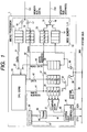
- Fig. 1 is a block diagram for showing details of the interior construction of a micro-processor according to a first embodiment of the present invention.
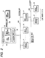
- Fig. 2 is a system construction view for showing an outline of the data transfer system according to the first embodiment of the present invention.
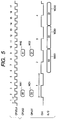
- Fig. 3 shows timing charts for showing two transfer methods on the system bus according to the present invention.
- Figs. 4 and 5 show timing charts for showing transfer timing of data in the system, being synchronized with internal clock (CPUCLK) of the micro-processor and a clock (CLK) of the system bus, according to the first embodiment of the present invention
- Fig. 6 is a flow chart for showing control processes in selection of data transfer methods of the micro-processor, according to the first embodiment of the present invention.
- Fig. 7 is a flow chart for showing control processes corresponding to the chart of Fig. 6.
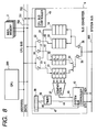
- Fig. 8 is a block diagram for showing details of a system according to a second embodiment of the present invention and a bus converter used therein.
- a micro-processor 1 having two systems of bus interfaces, i.e., a main memory bus (memory bus) and a system bus (I/O bus) according to the present invention, is constructed with a main memory bus interface 10, a system bus interface 30, and a CPU core portion 50 for executing various calculating processes.
- main memory bus memory bus
- I/O bus system bus
- the main memory bus interface 10 has a data buffer 11 for main memory read access, a data buffer 12 for main memory write access, an address buffer 13 for main memory access, an address buffer 14 for the direct memory access (DMA), a selector 15, an input buffer 16, and output buffers 17 and 18.
- DMA direct memory access
- the data buffer 11 for main memory read access functions as a data buffer being able to store a plurality of sets of data which are sent from the main memory through a memory bus (data) 701.
- the data buffer 12 for main memory read access functions as a data buffer being able to store a plurality of sets of data which are sent to the main memory through the memory bus (data) 701.
- the address buffer 13 for main memory access functions as an access address buffer being able to store a plurality of sets of access addresses which are sent to the main memory through a memory bus (address) 702.
- the address buffer 14 for direct memory access (DMA) functions as the access address buffer being able to store a plurality of sets of access addresses which are sent from a system bus to the main memory through the memory bus (address) 702.
- the system bus interface 30 has an address buffer 31 for PIO access, a data buffer 32 for PIO write access, a data buffer 33 for PIO read access, a selector 34, an output buffer 35, an input buffer 36, an address comparator 37, a built-in control register 38, a timer 39, a system bus controller 40, a PIO access address and main memory access address line 41, a PIO and main memory write access data line 42, a PIO read data line 43, and control lines 44, 45, 46 and 47.
- the address buffer 31 for PIO access functions as a write address buffer being able to store a plurality of sets of write addresses to the system bus 800.
- the data buffer 32 for PIO write access functions as a write data buffer being able to store a plurality of sets of write data to the system bus 800.
- the data buffer 33 for PIO read access has a function as a read data buffer being able to store a plurality of sets of read data from the system bus 800.
- the address comparator 37 has a function for deciding whether the access requirements coming on the heels of the other or before and after about the time have the continuous write addresses coming before and after about the time, among the access requirements which are stored in the address buffer 31 for PIO access, i.e., it decides whether the PIO addresses coming before and after about the time are those for the continuing addresses or not.
- the built-in control register 38 sets up a counting time period for the timer 39 with the setup value thereof.
- the timer 39 counts the distance between the PIO addresses coming before and after about the time so as to set up a boundary time period for keeping the issuance of the burst transfer onto the system but 800.
- the system bus controller 40 has a function for converting a plurality of writing operations onto the continuing addresses into a burst transfer protocol by which they can be transfer with a series of the continuous data cycles following one (1) address cycle, when detecting them coming before and after about the time to have the continuing write addresses in the access requirements which are stored in the buffer 31, by controlling the system bus accesses.
- micro-processor 1 has a selector 20 and a main memory read data line 21.
- the micro-processor 1 having the two (2) bus interfaces i.e., the main memory bus (memory bus) and the system bus (I/O bus) according to the present invention, is connected to the data line 701 of the main memory bus (memory bus) through the main memory bus interface 10, and to the address line 702 of the main memory bus (memory bus), thereby being connected to the system bus (I/O bus) 800 through the system bus interface 30.
- the main memory read data line 21 transfers the main memory read data from the data buffer 11 for main memory read access through the selector 20 to the CPU core portion 50.
- the PIO access address and main memory access address line 41 transfers the access address from the CPU core portion 50 to the address buffer 31 for PIO access and the address buffer 13 for main memory access.
- the PIO and main memory write access data line 42 transfers the access address from the CPU core portion 50 to the data buffer 32 for PIO write access and the data buffer 12 for main memory write access.
- the PIO read data line 43 transfers the PIO read data from the data buffer 33 for PIO read access through the selector 20 to the CPU core portion 50.
- the control line 44 transfers a control signal from the timer 39 to the system bus controller 40.
- the control line 45 transfers a control signal from the address comparator 37 to the system bus controller 40.
- the control line 46 transfers a control signal from the built-in control register 38 to the timer 39.
- the control line 47 transfers the control signal between the built-in control register 38 and the system bus controller 40.
- the output of the address buffer 13 for main memory access and the output of the address buffer 14 for direct memory access (DMA) are outputted through the selector 15 and the output buffer 18 to the memory bus address line 702.
- the output of the address buffer 12 for main memory access is outputted through the output buffer 17 to the memory bus data line 701.
- From the memory data line 701 is inputted the main memory data through the input buffer 16 into the data buffer 11 for main memory read access.
- the output of the address buffer 31 for PIO access is outputted to the address comparator 37.
- the output of the address buffer 31 for PIO access and the output of the data buffer 32 for PIO write access are outputted through the selector 34 and the output buffer 35 to the system bus (I/O bus) 800.
- the data for PIO read access is inputted through the input buffer 36 into the data buffer 33 for PIO read access and the address buffer 14 for direct memory access (DMA).
- DMA direct memory access
- the data transfer system is constructed with the micro-processor 1, the main memory 2, a high or middle speed IO (input/output) device 7, such as a display system, etc., the bus converter for executing the protocol conversion between the system bus and the (I/O bus, a low speed IO device 9, the main memory (memory) bus 700, the system bus, and the I/O bus 900.
- the micro-processor 1 the main memory 2
- a high or middle speed IO (input/output) device 7 such as a display system, etc.
- the bus converter for executing the protocol conversion between the system bus and the (I/O bus, a low speed IO device 9
- main memory (memory) bus 700 main memory
- the system bus and the I/O bus 900.
- the micro-processor 1 has the main memory bus interface 10, the system bus interface 30, and the CPU core portion 50.
- the high or middle speed IO (input/output) device 7 there are provided the display devices 71 and 72, and so on.
- the low speed IO device 9 there are provided the display device 91 and an input device 92.
- a case is considered where the PIO write accesses are executed continuously.
- the IO write addresses from the CPU core portion 50 are stored through an internal address line 41 into the buffer 31.
- the PIO write data from the CPU core portion 50 are stored through an other internal address line 41 into the buffer 32.
- the operating frequency within inside of the processor 1 is higher than that of the system bus 800, therefore, if there are given the PIO write access requirements with continuity, the next PIO write access is stored into the buffers 31 and 32 before the timing of initiating the system bus 800.
- those continuous two addresses of the PIO write accesses are compared by the address comparator 37. If they are continuous in the addresses thereof, the system bus controller 40 executes such the control of converting them into the burst transfer to be transferred onto the system bus.
- the timer 39 is one which counts the number of the waiting cycles for that purpose.
- This value is determined depending upon a ratio between the operating frequency inside the processor 1 and that of system bus 800. If it is necessary to determine whether there is the next data or not before the completion of the address cycle due to the regulation of the protocol of the system bus, it is possible to keep it for three (3) cycles with the clock (CPUCLK) of the processor, when the ratio of the operating frequency between the inside of processor and the system bus is 2:1, and it is also possible to keep it for seven (7) cycles with the clock (CPUCLK) of the processor, when the ratio of the operating frequency between the inside of processor and the system bus is 4:1.
- CPUCLK clock
- Fig. 3 shows the timing chart in the case where the single PIO write access is continued by four (4) times on the system bus
- Fig. 3 (b) shows the timing chart of the burst PIO write access of the four (4) data cycles for the continuing addresses.
- the system bus controller 40 outputs ADV-N and DTV-N, alternatively, and the write addresses A 0 - A 4 and the write data D 0 - D 4 are sent out to the system bus 800, alternatively.
- the system bus controller 40 outputs the burst-like DTV-N after outputting the ADV-N, and the write data D 0 - D 4 having continuous addresses are sent out in the burst-like manner to the system bus 800 after the write address A 0 .
- the CPUCLK indicates the internal clock inside the micro-processor, the CPUAD the address data inside the micro-processor, the CPUDT the data inside the micro-processor, the CLK the clock on the system bus, and the A/D the address data and the access data on the system bus, respectively.
- a first PIO write access address WA1 inside the micro-processor 1 and a first PIO write access data WD1 inside the micro-processor 1 are outputted with the CPU clock 2.
- a second PIO write access address WA2 inside the micro-processor 1 and a second PIO write access data WD2 inside the micro-processor 1 are outputted with the CPU clock 5.
- the first PIO write access address WAS1 on the system bus 800 is transferred onto the system bus 800 at the system bus clock 2, and the first PIO write access data WAD1 on the system bus is transferred with the system bus clock 3, and further the second PIO write access data WAD2 on the system bus 800 is transferred with the system bus clock 4, onto the system bus 800.
- the ratio between the operating frequency (CPUCLK) of the micro-processor 1 and the operating frequency (CLK) of the system bus 800 is set at 2:1.
- the first PIO write access address WA1 inside the micro-processor 1 and the first PIO write access data WD1 inside the micro-processor 1 are outputted with the CPU clock 2
- the second PIO write access address WA2 inside the micro-processor 1 and the second PIO write access data WD2 inside the micro-processor 1 are outputted with the CPU clock 9.
- the first PIO write access address WAS1 on the system bus 12 is transferred with the system bus clock 2
- the first PIO write access data WDS1 on the system bus 12 is with the system bus clock 3
- the second PIO write access data WDS2 on the system bus 12 with the system bus clock 4 onto the system bus 800.
- the ratio between the operating frequency (CPUCLK) of the micro-processor 1 and the operating frequency (CLK) of the system bus 12 is set at 4:1.
- Fig. 6 shows the flow chart for showing control process of the micro-processor.
- the address comparator 37 determines there is the continuity in the addresses between it and the first access or not (S4). If there is no continuity in the addresses, the second PIO access is also treated as the single PIO access, and the PIO address and the data thereof are transferred (S11).
- the timer is reset (S5) to watch the arrival of a third access (S6).
- the first two accesses are converted into the burst protocol, and the PIO addresses and the data thereof are transferred (S12).
- the timer is reset (S8) so as to watch the arrival of a fourth access (S9).
- the first three accesses are converted into the burst protocol, and the PIO addresses and the data thereof are transferred (S13).
- the fourth access is converted into the burst protocol, and the PIO address and the data thereof are transferred (S14).
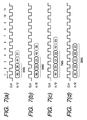
- Fig. 7 shows the single PIO write access cycle SWS which is processed in the step S11, and Fig. 7 (b) shows the burst PIO write access cycle DWS of two data which is processed in the step S12.
- Fig. 7 (c) shows the burst PIO write access cycle TWS of three data which is processed in the step S13
- Fig. 7 (d) shows the burst PIO write access cycle QWS of four data which is processed in the step S14.
- the CPU and the system bus are connected to each other through the bus converter 8 between the CPU and the system, however, in the first embodiment, such the processor 1 is adopted as shown in Fig. 2, which builds the system bus interface portion 30 therein, by taking the efficiency of data delivery into consideration.
- the system bus interface portion 30 is independent upon the processor 1.
- the second embodiment is for the bus converter in case of applying the CPU having only one system of the bus interface.
- the bus converter 8 is connected to a CPU 500 and the main memory 2 through a CPU bus 750, and also to the system bus 800 as well.
- the CPU 500 has the only one system of the bus interface.
- the bus converter 8 executes the protocol conversion between the CPU bus 750 and the system bus 800.
- the CPU bus 750 is constructed with an address line 751 and a data line 752.
- the bus converter 8 is so constructed to have the address buffer 14 for main memory access, an input buffer 17, output buffers 18 and 22, an input buffer 23, an internal address line 24, an address buffer 33 for main memory access, a selector 34, an output buffer 35, an input buffer 36, an address comparator 37, a built-in control register 38, a timer 39, a system bus controller 40, an internal address line 41, an internal data line 42, an internal data line 43, a control line 45, 46 and 47 and a CPU bus 49.
- the address comparator 37 decides whether the PIO addresses coming before and after about the time are those for the continuing addresses or not.
- the timer 39 counts the distance between the PIO addresses coming on the heels of the other.
- the system bus controller 40 controls the system bus accesses.
- the CPU bus controller 49 also controls the system bus accesses.
- the write access address from the CPU 500 is transferred to the address buffer 31 for PIO access through the CPU bus (address) 751, the input buffer 23 and the PIO access address line 41.
- the write access data is transferred to the data buffer 32 for PIO write access through the CPU bus (data) 752, the input buffer 17 and the PIO and main memory write access data line 42.
- the access address output of the address buffer 31 for PIO access and the data output of the data buffer 32 for PIO write access are sent out to the system bus 800 through the selector 34 and the output buffer 35, according to the processing of the present invention.
- the PIO read data from the data buffer 33 for PIO read access is sent to the main memory 2 through the PIO read data lien 43, the output buffer 22 and the CPU bus (data) 752.
- the output of the address buffer 14 for main memory access is outputted to the main memory 2 through the internal address line 24, the output buffer 18 and the CPU bus (address) 751.
- the data for PIO read access which is inputted from the system bus 800 through the input buffer 36 is further inputted into the data buffer 33 for PIO read access, and the access address thereof is inputted into the address buffer 14 for main memory access.
- the control line 44 transfers a control signal from the timer 39 to the system bus controller 40.
- the control line 45 transfers a control signal from the address comparator 37 to the system bus controller 40.
- the control line 46 transfers a control signal from the built-in control register 38 to the timer 39.
- the control line 47 transfers a control signal between the built-in control register 38 and the system bus controller 40.
- the output of the address buffer 31 for PIO access is outputted to the address comparator 37.
- the PIO access address and transfer method are carried out in the same manner as in the first embodiment.
- the transfer requirements, coming from the bus of the other hierarchy through the bus converter 8 after the bus-conversion thereof, for example, the PIO accesses which are accessed to the system bus from the other processor through the bus converter, can be issued after being converted into the burst protocol transfer on the system bus when it is one for the continuous addresses, thereby enabling the improvement of the data efficiency on the bus.
Landscapes
- Engineering & Computer Science (AREA)
- Theoretical Computer Science (AREA)
- Physics & Mathematics (AREA)
- General Engineering & Computer Science (AREA)
- General Physics & Mathematics (AREA)
- Bus Control (AREA)
Abstract
Description
Claims (11)
- A processor for an information processing equipment having a unit for executing calculation processes, comprising:a buffer (31, 32) for storing plural sets of write addresses for a system bus (800) of said information processing equipment and data corresponding to said write addresses;a comparator (37) for deciding whether or not there are write addresses in succession in the write addresses stored in said buffer (31, 32); andmeans (45) for converting respective writing operations of the plural data, corresponding to said continuous write addresses in succession, into burst transfer protocol which can be transferred with a series of continuing data cycles following one address cycle, when the continuous write addresses are detected by said comparator (37).
- The processor of claim 1, further comprising means for initialising the transfer of write data with a delay of a predetermined time period, when the write addresses are detected to be in succession within said write address buffer (31) by said comparator (37) by comparison with the case when no write addresses are detected in succession.
- The processor of claim 1, wherein, when there is a transfer requirement of new write data to said processor within said predetermined time period, said comparator (37) decides whether the write address corresponding to said new write data is continuous with any one of the write addresses which are detected to be in succession.
- A processor for an information processing equipment having means for executing calculation processes and being connected to a multiplex bus with which address and data are used in a time-sharing manner, comprising:a write address buffer (31) for storing plural write addresses which are transferred using said multiplex bus;a write data buffer (32) for storing plural data which are transferred using said multiplex bus;a comparator (37) for deciding whether or not there is continuity in the write addresses stored in said write buffer; andmeans (45) for converting writing operations of the plural write data stored in said write data buffer (32), corresponding to said write addresses detected to be continuous, into burst transfer protocol which can be transferred at a series of continuous data cycles following one address cycle, when the continuous write addresses are detected by said comparator (37), wherein said plural write data are transferred by the writing operations which are converted into said burst transfer protocol.
- The processor of claim 4, further comprising means for initialising the transfer of write data with a delay of a predetermined time period when the write addresses are detected to be continuous within said write address buffer (31) by said comparator (37) by comparison with the case when no write addresses are detected as continuous.
- The processor of claim 4, wherein, when there is a transfer requirement of new write data to said processor within said predetermined time period, said comparator (37) decides whether the write address corresponding to said new write data is continuous with any one of the write addresses which are detected to be continuous.
- The processor of claim 1 or 4, wherein said comparator (37) decides whether or not the addresses stored next to each other in said buffer (31, 32) are in succession.
- The processor of claim 1 or 4, wherein said plural write data are transferred from said bus through a bus converter to a bus which is different from said multiplex bus.
- The processor of claim 1 or 4, further comprising means for selectively setting up a value of said predetermined time period.
- The processor of claim 1 or 4, wherein said processor is integrated on a single chip.
- A control method of a processor for an information processing equipment having a unit for executing calculation processes therein, wherein at least one bus, which is connected as an input/output means to an outside of said processor, is a multiplex bus with which address and data are used in a time-sharing manner, and said processor has a burst transfer protocol which can be transferred with a series of continuous data cycles following one address cycle, a write address buffer (31) for storing plural sets of write addresses for said bus, a write data buffer (32) for storing plural sets of write data for said bus, a comparator (37) for deciding whether or not access requirements coming before and after about same time to each other are continuos in the write addresses thereof, and means (45) for converting plural write operations for the continuous addresses into burst transfer protocol which can be transferred at a series of continuing data cycles following one address cycle, wherein, when detecting the access requirements coming before and after about same time to each other, being continuous in the write addresses thereof, the plural write operations for said continuing addresses are converted into the burst transfer protocol which can be transferred at the series of continuing data cycles following the one address cycle.
Applications Claiming Priority (2)
| Application Number | Priority Date | Filing Date | Title |
|---|---|---|---|
| JP10034541A JPH11232214A (en) | 1998-02-17 | 1998-02-17 | Processor for information processor and its controlling method |
| JP3454198 | 1998-02-17 |
Publications (2)
| Publication Number | Publication Date |
|---|---|
| EP0939374A2 true EP0939374A2 (en) | 1999-09-01 |
| EP0939374A3 EP0939374A3 (en) | 2000-05-24 |
Family
ID=12417168
Family Applications (1)
| Application Number | Title | Priority Date | Filing Date |
|---|---|---|---|
| EP99103056A Withdrawn EP0939374A3 (en) | 1998-02-17 | 1999-02-16 | Processor for information processing equipment and control method |
Country Status (5)
| Country | Link |
|---|---|
| US (1) | US6728813B1 (en) |
| EP (1) | EP0939374A3 (en) |
| JP (1) | JPH11232214A (en) |
| KR (1) | KR100288036B1 (en) |
| TW (1) | TW434485B (en) |
Families Citing this family (9)
| Publication number | Priority date | Publication date | Assignee | Title |
|---|---|---|---|---|
| JP2002366509A (en) * | 2001-06-06 | 2002-12-20 | Mitsubishi Electric Corp | Direct memory access controller and its access control method |
| US20040064662A1 (en) * | 2002-09-26 | 2004-04-01 | Analog Devices, Inc. | Methods and apparatus for bus control in digital signal processors |
| JP2006243890A (en) * | 2005-03-01 | 2006-09-14 | Nec Corp | Bus bridge, data transfer method and program |
| KR101601291B1 (en) * | 2010-06-28 | 2016-03-08 | 현대자동차주식회사 | Knee bolster for vehicle |
| JP5318080B2 (en) * | 2010-12-10 | 2013-10-16 | 三菱電機株式会社 | Data processing device |
| JP5387993B2 (en) * | 2011-04-19 | 2014-01-15 | 日本電気株式会社 | Data transfer control device, data transfer control method, and computer system |
| CN112559397A (en) * | 2019-09-26 | 2021-03-26 | 阿里巴巴集团控股有限公司 | Device and method |
| US11262226B2 (en) | 2020-02-17 | 2022-03-01 | GWU Design | Hybrid mass flow sensor including a thermal and coriolis principle measurement arrangements |
| CN114036096B (en) * | 2021-11-04 | 2024-05-03 | 珠海一微半导体股份有限公司 | Read controller based on bus interface |
Citations (6)
| Publication number | Priority date | Publication date | Assignee | Title |
|---|---|---|---|---|
| JPH0512197A (en) * | 1991-07-03 | 1993-01-22 | Hitachi Ltd | Bus control system |
| JPH05324544A (en) * | 1992-05-15 | 1993-12-07 | Hitachi Ltd | Bus control method |
| EP0629956A2 (en) * | 1993-05-28 | 1994-12-21 | International Business Machines Corporation | Bus-to-bus bridge for optimising data transfers between a system bus and a peripheral bus |
| US5550996A (en) * | 1992-11-02 | 1996-08-27 | Kabushiki Kaisha Toshiba | ROM burst transfer continuous read-out extension method and a microcomputer system with a built-in ROM using this method |
| JPH09134326A (en) * | 1995-11-10 | 1997-05-20 | Toshiba Corp | Computer system |
| US5941960A (en) * | 1993-11-16 | 1999-08-24 | Intel Corporation | Host initiated PCI burst writes utilizing posted write buffers |
Family Cites Families (8)
| Publication number | Priority date | Publication date | Assignee | Title |
|---|---|---|---|---|
| US5146582A (en) * | 1989-06-19 | 1992-09-08 | International Business Machines Corp. | Data processing system with means to convert burst operations into memory pipelined operations |
| DE69123987T2 (en) * | 1990-01-31 | 1997-04-30 | Hewlett Packard Co | Push operation for microprocessor with external system memory |
| US5276684A (en) * | 1991-07-22 | 1994-01-04 | International Business Machines Corporation | High performance I/O processor |
| US5983275A (en) * | 1994-05-04 | 1999-11-09 | Cirrus Logic, Inc. | Apparatus for and method of providing interrupts to a host processor in a frame receiving system |
| KR0171942B1 (en) * | 1995-06-30 | 1999-03-30 | 김주용 | Burst length detection circuit |
| US5708814A (en) * | 1995-11-21 | 1998-01-13 | Microsoft Corporation | Method and apparatus for reducing the rate of interrupts by generating a single interrupt for a group of events |
| JPH10124447A (en) * | 1996-10-18 | 1998-05-15 | Fujitsu Ltd | Data transfer control method and device |
| US5943479A (en) * | 1997-01-02 | 1999-08-24 | Digital Equipment Corporation | Method for reducing the rate of interrupts in a high speed I/O controller |
-
1998
- 1998-02-17 JP JP10034541A patent/JPH11232214A/en active Pending
-
1999
- 1999-02-12 TW TW088102348A patent/TW434485B/en active
- 1999-02-12 KR KR1019990005004A patent/KR100288036B1/en not_active IP Right Cessation
- 1999-02-16 US US09/250,156 patent/US6728813B1/en not_active Expired - Fee Related
- 1999-02-16 EP EP99103056A patent/EP0939374A3/en not_active Withdrawn
Patent Citations (6)
| Publication number | Priority date | Publication date | Assignee | Title |
|---|---|---|---|---|
| JPH0512197A (en) * | 1991-07-03 | 1993-01-22 | Hitachi Ltd | Bus control system |
| JPH05324544A (en) * | 1992-05-15 | 1993-12-07 | Hitachi Ltd | Bus control method |
| US5550996A (en) * | 1992-11-02 | 1996-08-27 | Kabushiki Kaisha Toshiba | ROM burst transfer continuous read-out extension method and a microcomputer system with a built-in ROM using this method |
| EP0629956A2 (en) * | 1993-05-28 | 1994-12-21 | International Business Machines Corporation | Bus-to-bus bridge for optimising data transfers between a system bus and a peripheral bus |
| US5941960A (en) * | 1993-11-16 | 1999-08-24 | Intel Corporation | Host initiated PCI burst writes utilizing posted write buffers |
| JPH09134326A (en) * | 1995-11-10 | 1997-05-20 | Toshiba Corp | Computer system |
Non-Patent Citations (3)
| Title |
|---|
| PATENT ABSTRACTS OF JAPAN vol. 017, no. 280 (P-1547), 28 May 1993 (1993-05-28) & JP 05 012197 A (HITACHI LTD), 22 January 1993 (1993-01-22) * |
| PATENT ABSTRACTS OF JAPAN vol. 018, no. 153 (P-1709), 14 March 1994 (1994-03-14) & JP 05 324544 A (HITACHI LTD), 7 December 1993 (1993-12-07) * |
| PATENT ABSTRACTS OF JAPAN vol. 1997, no. 09, 30 September 1997 (1997-09-30) & JP 09 134326 A (TOSHIBA CORP), 20 May 1997 (1997-05-20) * |
Also Published As
| Publication number | Publication date |
|---|---|
| KR100288036B1 (en) | 2001-04-16 |
| TW434485B (en) | 2001-05-16 |
| KR19990072646A (en) | 1999-09-27 |
| JPH11232214A (en) | 1999-08-27 |
| US6728813B1 (en) | 2004-04-27 |
| EP0939374A3 (en) | 2000-05-24 |
Similar Documents
| Publication | Publication Date | Title |
|---|---|---|
| US4368514A (en) | Multi-processor system | |
| US6282598B1 (en) | PCI bus system wherein target latency information are transmitted along with a retry request | |
| US6425037B1 (en) | Information processing system, bus arbiter, and bus controlling method | |
| EP0508634B1 (en) | Memory access for data transfer within an I/O device | |
| EP0293860A2 (en) | Peripheral controller and adapter interface | |
| EP0476872B1 (en) | Work station including interfacing means for transferring data between first and second buses | |
| US5542110A (en) | DMA controller which releases buses to external devices without relinquishing the bus utility right | |
| US5721882A (en) | Method and apparatus for interfacing memory devices operating at different speeds to a computer system bus | |
| US6728813B1 (en) | Method and apparatus for converting non-burst write cycles to burst write cycles across a bus bridge | |
| US5857082A (en) | Method and apparatus for quickly transferring data from a first bus to a second bus | |
| US6272583B1 (en) | Microprocessor having built-in DRAM and internal data transfer paths wider and faster than independent external transfer paths | |
| US5627968A (en) | Data transfer apparatus which allows data to be transferred between data devices without accessing a shared memory | |
| US5799161A (en) | Method and apparatus for concurrent data routing | |
| US20030236941A1 (en) | Data processor | |
| US6032238A (en) | Overlapped DMA line transfers | |
| EP0478148B1 (en) | Work station including a direct memory access controller | |
| JPH07295947A (en) | Equipment and method for data transfer management | |
| US6483753B1 (en) | Endianess independent memory interface | |
| JP3420114B2 (en) | Data transfer method | |
| JPH09223103A (en) | Information processing system | |
| EP0365114A2 (en) | Interface arrangement for interfacing a data storage device with a data handling system | |
| JP2534321B2 (en) | Data transfer control method and apparatus | |
| US5581793A (en) | System for bypassing setup states in a bus operation | |
| JP2790668B2 (en) | Data transfer control method | |
| JP3523384B2 (en) | Data transfer method and computer system |
Legal Events
| Date | Code | Title | Description |
|---|---|---|---|
| PUAI | Public reference made under article 153(3) epc to a published international application that has entered the european phase |
Free format text: ORIGINAL CODE: 0009012 |
|
| AK | Designated contracting states |
Kind code of ref document: A2 Designated state(s): DE FR GB IT NL |
|
| AX | Request for extension of the european patent |
Free format text: AL;LT;LV;MK;RO;SI |
|
| PUAL | Search report despatched |
Free format text: ORIGINAL CODE: 0009013 |
|
| AK | Designated contracting states |
Kind code of ref document: A3 Designated state(s): AT BE CH CY DE DK ES FI FR GB GR IE IT LI LU MC NL PT SE |
|
| AX | Request for extension of the european patent |
Free format text: AL;LT;LV;MK;RO;SI |
|
| 17P | Request for examination filed |
Effective date: 20001124 |
|
| AKX | Designation fees paid |
Free format text: DE FR GB IT NL |
|
| STAA | Information on the status of an ep patent application or granted ep patent |
Free format text: STATUS: THE APPLICATION HAS BEEN WITHDRAWN |
|
| 18W | Application withdrawn |
Effective date: 20071220 |