EP0932258B1 - Method and circuit for digital modulation and method and circuit for digital demodulation - Google Patents
Method and circuit for digital modulation and method and circuit for digital demodulation Download PDFInfo
- Publication number
- EP0932258B1 EP0932258B1 EP97943166A EP97943166A EP0932258B1 EP 0932258 B1 EP0932258 B1 EP 0932258B1 EP 97943166 A EP97943166 A EP 97943166A EP 97943166 A EP97943166 A EP 97943166A EP 0932258 B1 EP0932258 B1 EP 0932258B1
- Authority
- EP
- European Patent Office
- Prior art keywords
- bits
- data
- block data
- translation
- block
- Prior art date
- Legal status (The legal status is an assumption and is not a legal conclusion. Google has not performed a legal analysis and makes no representation as to the accuracy of the status listed.)
- Expired - Lifetime
Links
Images


Classifications
-
- H—ELECTRICITY
- H03—ELECTRONIC CIRCUITRY
- H03M—CODING; DECODING; CODE CONVERSION IN GENERAL
- H03M7/00—Conversion of a code where information is represented by a given sequence or number of digits to a code where the same, similar or subset of information is represented by a different sequence or number of digits
- H03M7/14—Conversion to or from non-weighted codes
-
- H—ELECTRICITY
- H03—ELECTRONIC CIRCUITRY
- H03M—CODING; DECODING; CODE CONVERSION IN GENERAL
- H03M13/00—Coding, decoding or code conversion, for error detection or error correction; Coding theory basic assumptions; Coding bounds; Error probability evaluation methods; Channel models; Simulation or testing of codes
- H03M13/31—Coding, decoding or code conversion, for error detection or error correction; Coding theory basic assumptions; Coding bounds; Error probability evaluation methods; Channel models; Simulation or testing of codes combining coding for error detection or correction and efficient use of the spectrum
-
- H—ELECTRICITY
- H03—ELECTRONIC CIRCUITRY
- H03M—CODING; DECODING; CODE CONVERSION IN GENERAL
- H03M5/00—Conversion of the form of the representation of individual digits
- H03M5/02—Conversion to or from representation by pulses
- H03M5/04—Conversion to or from representation by pulses the pulses having two levels
- H03M5/14—Code representation, e.g. transition, for a given bit cell depending on the information in one or more adjacent bit cells, e.g. delay modulation code, double density code
- H03M5/145—Conversion to or from block codes or representations thereof
Description
- The present invention relates to a digital modulation circuit, a digital modulation method, a digital demodulation circuit and a digital demodulation method. More specifically, the present invention relates to a digital modulation circuit and a digital modulation method for modulating an unknown data sequence to a recording signal waveform sequence or channel sequence to be recorded on a recording medium, and to a digital demodulation circuit and a digital demodulation method for demodulating the signal waveform sequence to a data sequence.
- A binary data sequence is modulated to an appropriate recording signal waveform sequence and recorded on a recording medium. For example, a binary data sequence is subjected to RLL coding and further to NRZI modulation to be recorded on the recording medium. This enhances recording density. The binary data sequence may sometimes be, directly subjected to NRZ modulation or NRZI modulation to be recorded on the recording medium.
- In RLL coding, datawords of m bits each are successively cut out from an input data sequence, and each dataword is translated to a codeword each of n bits. This translation has a condition for enlarging a minimum value Tmin and reducing a maximum value Tmax of a time interval between adjacent transitions of the NRZI modulated recording signal. More specifically, there is a condition that in the RLL coded code sequence, the number of bits of "0" existing between a bit "1" and another bit "1" must be at least d and at most k. The RLL code translated to satisfy the condition is referred to as (d, k; m, n) RLL code.
- In NRZI modulation, an RLL code is modulated such that bit "1" is inverted and bit "0" is not inverted. Accordingly, bit inversion interval in the signal to be recorded after NRZI modulation becomes wider than the bit inversion interval in the RLL code before NRZI modulation. Therefore, as compared with when the RLL code before NRZI modulation is recorded on a recording medium and reproduced, waveform distortion in the reproduced signal can be reduced when the recording signal after NRZI modulation is recorded on the recording medium and reproduced, and as a result, error in reading can be reduced. When error in recording of approximately the same extent is tolerable, higher recording density can be attained when the recording signal after NRZI modulation is recorded on the recording medium, than when the recording signal before NRZI modulation is on the recording medium.
- Desired features of the recording signal waveform sequence are as follows.
- Tmin is calculated as a product of "d+1" and duration of channel bit, that is, a detection window width Tw. When recording density is made higher, inversion interval of recording signals becomes smaller, so that the reproduced signals are more susceptible to distortion because of intersymbol interference. As a result, error in reading is more likely. In order to reduce waveform distortion in reading from a recording medium with high recording density and to reduce error in recording, larger Tmin is desirable.
- Tmax is calculated as a product of "k+1" and the detection window width Tw. A reproduction pulse cannot be obtained unless the polarity is inverted. Therefore, a clock cannot be directly generated from the reproduction pulse, which leads to clocks of lower accuracy. When the interval of polarity inversion becomes longer, there will be much fluctuation in DC component, and therefore smaller Tmax is desirable.
- A recording apparatus and a reproducing apparatus have an AC coupling device. Therefore, when the recording signal has a DC component, recording signal waveform is distorted in the AC coupling device, which is not desirable. Further, it is not possible to recover in reproduction the DC component lost at the time of recording. Therefore, less DC component and less low frequency component are desired.
- For evaluation of the DC component and the low frequency component in the recording signal, DSV (digital Sum Value) is used. DSV represents an accumulated value calculated from the start point of the waveform sequence of the recording signal, with the value of bit "1" regarded as "+1" and the value of bit "0" as "-1". If the absolute value of DSV is small, it means that the DC component or the low frequency component is small. For evaluation of the DC component and the low frequency component of each code, CDS (Codeword Digital Sum) is used. CDS represents DSV in each codeword, and smaller CDS represents smaller DC component or low frequency component of the corresponding codeword.
- Detection window width Tw is given by (m/n)T, which represents a time which can be used for detection of a reproduction bit, that is, resolution. Further, the detection window width Tw represents window margin against phase fluctuation of the reproduced signal caused by waveform or intersymbol interference or noise, and larger value is desirable.
- In order to improve Tmin, Tmax and DSV, sometimes coding is performed with reference to preceding and succeeding codewords. The length of the preceding or succeeding codeword referred to at that time is called constraint length Lc. As Lc becomes larger, error propagation becomes larger and circuit configuration becomes more complicated. Therefore, smaller Lc is desired.
- Japanese Patent Laying-Open No. 52-128024 discloses a technique for making Tmin larger and making Tmax smaller in the recording signal after NRZI modulation. According to this Laid-Open application, by RLL coding in which datawords each of 2 bits are successively cut out from an input data sequence and translated to codewords each of 3 bits, (1, 7; 2, 3) RLL codes are produced. Code sequences of thus produced RLL code are subjected to NRZI modulation. When the condition of d=1 cannot be satisfied, (1, 7; 4, 6) RLL codes are produced.
- Japanese Patent Publication No. 1-27510 discloses a technique of coding (RLL coding) for reducing DC component of the recording signal after NRZI modulation, in which coding is performed so as not to reduce Tmin of the recording signal after NRZI modulation. According to this published application, blocks each of n bits are successively cut out from a code sequence after coding, and between adjacent blocks, redundancy bits each consisting of a plurality of bits are inserted. The code sequence with redundancy bits inserted is supplied to an NRZI modulation circuit. Here, redundancy bits are selected dependent on whether code inversion is necessary between the blocks to which the redundancy bits are to be inserted, and on the state of the last part of the immediately preceding block. More specifically, the redundancy bits are selected so as to reduce DC component of the NRZI modulated recording signal and not to reduce Tmin.
- Further, Japanese Patent Publication No. 5-34747 discloses a coding scheme in which rule of translation, i.e. a look-up table for translating a data sequence to RLL codes is adjusted in accordance with arrangement of data sequence, whereby Tmin of 1.5T, Tmax of 4.5T and Lc of 5T can be attained.
- Japanese Patent Publication No. 4-77991 discloses a technique for reducing DC component of the recording signal after NRZI modulation and to enlarge Tmin. According to this published application, datawords each of 8 bits are successively cut out from an input data sequence, and each dataword is translated to codewords each of 14 bits. Translation is performed such that in the translated code sequence, the number of bits of "0" is at least 1 and at most 8 between a bit "1" and another bit "1". There are two tables prepared for translating a dataword of 8 bits to a codeword of 14 bits, and dependent on the DSV at the end of the codeword that is translated immediately before, a codeword of either of the tables is selected. More specifically, selection is made to reduce DC component of the recording signal after NRZI modulation.
- Further, Japanese Patent Laying-Open No. 6-311042 discloses a technique for sufficiently reducing DC component of the recording signal after NRZI modulation and to improve recording density DR (density ratio) by enlarging Tmin. According to this Laid-Open application, datawords each of 8 bits are successively cut out from an input data sequence, and each dataword is translated to a codeword each of 17 bits. The translation is performed such that in the translated code sequence, the number of bits "0" existing between a bit "1" and another bit "1" is at least 2 and at most 9.
- The aforementioned codeword of 17 bits is obtained by adding redundancy bits of 2 bits, to a code of 15 bits corresponding to the dataword of 8 bits. According to the aforementioned Japanese Patent Laying-Open No. 6-311042, two tables specifying correspondence between the datawords of 8 bits each to codes of 15 bits each are prepared, and three different types of redundancy bits each of 2 bits are prepared. By a 17 bit codeword selected based on the DSV at the end of the data translated immediately before from six different codewords obtained by the combination of these two tables and three different types of redundancy bits, said dataword of 8 bits is replaced. More specifically, said 8 bit dataword is replaced by a 17 bit codeword selected to reduce the DC component of the recording signal after NRZI modulation.
- In the techniques disclosed in the aforementioned applications, in order to suppress DC component or low frequency component of the recording signal, a technique of adding redundancy bits or preparing a plurality of translation tables to select an optimal translation table in accordance with the input dataword, for example, are used. Accordingly, the above described condition on "d" or "k" is become less severe, resulting in an inconvenience of Tmin becoming smaller or Tmax becoming larger. As the number of bits of the codeword increases, Tw becomes smaller, causing a problem that the minimum resolution becomes lower.
- EP-0593173-A2 discloses modulating by interleaved NRZI by inserting one bit per every n-bits of input data series, the frequency characteristics of bit rows varying by the polarity ("0" or "1") of the bit to be inserted are compared, and the bit row closer to the desired frequency characteristic is selected as output series, so that recording is effected by controlling the frequency characteristics of the digital signal.
- EP-0415853-A2 shows conventional NRZI modulation including several exclusive OR circuits.
- Therefore, a main object of the present invention is to provide a digital modulation circuit, a digital modulation method, a digital demodulation circuit and a digital demodulation method allowing sufficient suppression of DC component and low frequency component of the recording signal.
- Another object of the present invention is to provide a digital modulation circuit, a digital modulation method, a digital demodulation circuit and a digital demodulation method allowing sufficient suppression of DC component and low frequency component of the recording signal while preventing reduction of Tmin or enlargement of Tmax.
- A still further object of the present invention is to provide a digital modulation circuit, a digital modulation method, a digital demodulation circuit and a digital demodulation method allowing improvement of resolution by enlarging Tw, while sufficiently suppressing DC component and low frequency component of their recording signal.
- A still further object of the present invention is to provide a digital modulation circuit, a digital modulation method, a digital demodulation circuit and a digital demodulation method allowing reduction in error in reproduction and reduction of error propagation in reproduction.
- These objects are achieved by a method of digital modulation according to
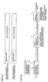
claim 1 and by a digital modulation circuit according toclaim 5, respectively; the remaining claims are related to further developments of the invention. - Figs. 1A and 1B are illustrations representing concept of the present invention.
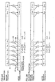
- Figs. 2A and 2B are illustrations representing translation and reverse translation by convolution operation shown in Figs. 1A and 1B.
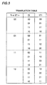
- Fig. 3 shows an example of data translation and reverse translation using a translation table.
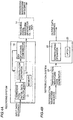
- Figs. 4A and 4B are schematic block diagrams of an embodiment of the present invention.
- Figs. 5A to 5D represent an example in which initial data are distributed to input block by convolution operation.
- Fig. 6 is a block diagram of a modulator in accordance with another embodiment of the present invention.
- Fig. 7 is a block diagram showing another specific example of the modulator.
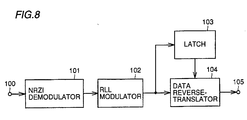
- Fig. 8 is a block diagram of a demodulator in accordance with an embodiment of the present invention.
- Fig. 9 is a block diagram showing another specific example of the modulator.
- Fig. 10 is a block diagram showing a still further example of the modulator.
- Fig. 11 shows another specific example of the demodulator.
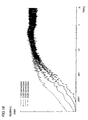
- Fig. 12 is a graph representing effect of suppression of DC component when initial data Tj having bit number t of 1, 2, 4 and 8 bits for the convolution operation are distributed as shown in Figs. 5A to 5D to be added to the input block of 80 bytes and (2, 7; 1, 2) RLL modulation is performed.
- Fig. 13 is a graph representing effect of suppression of DC component when (1, 7; 2, 3) RLL modulation is performed.
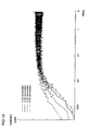
- Fig. 14 is a graph representing effect of suppressing DC component when initial data Tj having bit number t of 1, 2, 4 and 8 bits for convolution operation are distributed as shown in Figs. 5A to 5D and added to the input block of 40 bytes, and (1, 7; 2, 3) RLL modulation is performed.
- Fig. 15 is a graph representing effect of suppressing DC component when initial data Tj of bit number t of 1, 2, 4 and 8 bits for convolution operation are distributed as shown in Figs. 5A to 5D and added to the input block of 80 bytes, and RLL modulation is not performed.
- Fig. 16 is a graph representing effect of suppressing DC component when initial data Tj having the bit number t of 1, 2, 4 and 8 bits for convolution operation are distributed as shown in Fig. 5A to 5D and added to the input block of 160 bytes, and (2, 9; 8, 15) RLL modulation is performed.
- Fig. 17 is a graph representing effect of suppressing DC component when (1, 7; 2, 3) RLL modulation is performed in the similar manner.
- Fig. 18 is a graph representing effect of suppressing DC component when initial data Tj having bit number t of 1, 2, 4 and 8 bits for convolution operation are added to the input block of 40 bytes and RLL modulation is not performed.
- Fig. 19 is a graph representing effect of suppressing DC component when initial data Tj having bit number t of 1, 2, 4 and 8 bits for convolution operation are added to the input block of 160 bytes and RLL modulation is not performed.
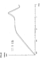
- Fig. 20 is a graph representing effect of suppressing high frequency component, when initial data Tj having bit number t of 8 bits for convolution operation is added to an input block of 80 bytes and (2, 7; 1, 2). RLL modulation is performed, and when (1, 7; 2, 3) RLL modulation is performed, with the abscissa normalized by a data bit frequency fb.
- Figs. 1A and 1B are illustrations representing the concept of the present invention.
- According to the present invention, a pre-translation data sequence A on which initial translation data is multiplexed by j different types of
initial data multiplexer 1 shown in Fig. 1A is applied to adata sequence translator 2 shown in Fig. 1B where convolution operation takes place to produce a translated data sequence B shown in Fig. 1A, and a desired recording waveform sequence is produced by adigital encoder 3. Here, initial data selection information which minimizes DC component (absolute value of DSV) in the recording waveform sequence is applied in advance by a DCcomponent measuring instrument 4 todata sequence translator 2, so that a recording block having minimum DC component is output. - Figs. 2A and 2B are illustrations representing translation and reverse translation by convolution operation shown in Figs. 1A and 1B. In Fig. 2A, respective data D0 to Du-1 represent data each consisting of t bits. Here, t bits may or may not be equal to m bits which are the unit of RLL modulation. RLL modulation may not be performed.
- At the time of data translation, at the head of data of each of the blocks, j different types of initial data (translation number Tj) is assigned and multiplexed by first assigning
means 31, and j different types of pre-translation block data are produced. The j different types of pre-translation block data are assigned by the second assigning means 32 to first operating means 33, starting from the leading code modulation unit except for initial data Tj, a current code modulation unit which is an object of translation and code modulation unit immediately preceding the current code modulation unit (initial data or translated code modulation unit) are subjected to exclusive OR operation by the first operating means 33, and replaced, by second operating means 34, with the current code modulation unit (convolution operation). The second operating means 34 also performs a process for setting the result of convolution operation as a preceding variable for the next convolution operation. - Consequently, j different types of translated block data are generated. More specifically, for each of j different types of pre-translation block data (multiplexed blocks), by mod2 operation of the head code modulation unit D0 and initial data Tj, translated data D'0 of the head code modulation unit except for the initial data is produced, which replaces D0. Thereafter, by mod2 operation of the above described translated code modulation unit data D'0 and the succeeding code modulation unit D1, the next translated data D'1 is produced in the similar manner, which replaces D1. Thereafter, in the similar manner, convolution operation including exclusive OR operation and replacement operation is repeated until the last code modulation unit of the corresponding block.
- In other words, for each of the j different types of pre-translation block data (multiplexed blocks), t bits at the head of the pre-translation block data and immediately following t bits are subjected to exclusive OR operation, the immediately following t bits are replaced by the result of operation, the replaced t bits and immediately following t bits are subjected to exclusive OR operation, the said immediately following t bits are replaced by the result of operation and thereafter, in the similar manner, convolution operation including the exclusive OR operation and the replacement operation is executed until the end of the pre-translation block data, whereby respective translated block data are produced from respective pre-translation block data (multiplexed blocks).
- At the time of data reverse-translation, as can be seen from Fig. 2B, starting from the demodulation code unit except for the leading modulation code unit (translation number Tj) of the pre-reverse-translation block data, the current demodulation code unit which is an object of reverse-translation and a demodulation code unit immediately preceding the current demodulation code unit (initial data or pre-reverse-translation demodulation code unit) are subjected to exclusive OR operation and the current demodulation code unit is replaced (convolution operation), and accordingly, reverse-translated block data is produced. More specifically, by mod2 operation of the head demodulation code unit D0 and initial data Tj, reverse-translated data D0 is produced, which replaces D'0. By mod2 operation of the aforementioned D'0 (pre-reverse-translation demodulation code unit) and the next demodulation code unit D'1, the next reverse-translated data D1 is produced in the similar manner, which replaces D'1. Thereafter, in the similar manner, the process is repeated until the last demodulation code unit of the corresponding block.
- In other words, the t bits at the head of the input block contributing to data reverse-translation ("before reverse translation " of Fig. 2B) and immediately following t bits are subjected to exclusive OR operation, the t bits at the head are replaced by the result of operation, the immediately following t bits and t bits following the said immediately following t bits are subjected to exclusive OR operation and the said immediately following t bits are replaced by the result of operation and thereafter, in the similar manner, convolution operation including the exclusive OR operation and the replacement operation is executed until the last of the input block, whereby the reverse-translated block of the input block is produced.
- In this manner, at the time of data reverse-translation, as one immediately preceding pre-translation demodulation code unit is used for reverse-translation of the current demodulation code unit, even when an error generates, the influence thereof is expanded only within the demodulation code unit and not propagated to succeeding demodulation code units. For example, when an error generates in the pre-reverse-translation demodulation code unit D'i, the influence of the error propagates only to the reverse-translated demodulation code unit Di and the unit Di+1.
- Fig. 3 shows an example of data translation and reverse-translation using a translation table. Fig. 3 represents a 2 bit translation table, which allows translation using four different types of Tj at most. More specifically, by using the translation table shown in Fig. 3, it is possible to find the translated demodulation code unit D'i, from immediately preceding translated demodulation code unit D'i-1 or initial data number Tj and pre-translation demodulation code unit Di. When RLL coding is to be performed after translation, generally, (d, k; m, n) RLL modulation may be performed on m bits of the sequence of demodulation code unit D'i of Fig. 3, and more specifically, data translation reverse translation may be performed using 3 bit data after (a, k: 2, n) RLL modulation in place of 2 bits of data. In this case also, the error propagates only to Di and D'i+1.
- Figs. 4A and 4B are schematic block diagrams of an embodiment of the present invention.
- In a recording system shown in Fig. 4A, an input data sequence is multiplexed by j different types of initial data Tj by j different type
initial data multiplexer 11, convolution operation is performed byconvolution operator 12, and DSV absolute values are compared by aDSV operating comparator 13. The translated block which has the minimum absolute value by comparison is selected, and subjected to NRZ modulation or NRZI modulation by a recordingsignal waveform generator 14 to be used as a recording waveform sequence. - In a reproduction system shown in Fig. 4B, a reproduced waveform sequence is translated to data by a reproduction
waveform data generator 21, subjected to convolution operation by aconvolution operator 22 and output as an output data sequence. - Figs. 5A to 5D represent examples of distribution of initial data to input blocks by convolution operation. In the example shown in Fig. 1B, j different types of initial data Tj are multiplexed at the head of the input block. In the examples shown in Figs. 5A to 5D, the initial data are multiplexed distributed within the block. More specifically, Fig. 5A shows an example in which 8 bits of initial data are multiplexed at the head of the input block, Fig. 5B shows an example in which the initial data are distributed 4 bits by 4 bits at two portions to be multiplexed, Fig. 5C shows an example in which the data are distributed 2 bits by 2 bits at four portions to be multiplexed and Fig. 5D shows an example in which the data are distributed bit by bit at eight portions to be multiplexed. Data translation efficiency is the same in any of these examples.
- Though degree of suppression of the DC component is approximately the same in Figs. 5A and 5B, the amount of operation in Fig. 5B is smaller than Fig. 5A, and the circuit configuration is more simple. Namely, when the example of Fig. 5B having the same data translation efficiency as the example of Fig. 5A is employed, sufficient effect of suppressing DC component can be attained by a relatively simple circuit.
- The initial data are divided into z as shown in the examples of Figs. 5A to 5D described above, it is reasonable to set the number of bits of each input divided block P=p/z and bit number of the divided initial data added to the head of each input divided block T=t/z to satisfy the range of "0.003≦ T/p≦0015".
- Fig. 6 is a block diagram of a modulator in accordance with another embodiment of the present invention. Referring to Fig. 6, an input block data of which code modulation unit consists of t bits are input from an
input terminal 90, and at the head of each one block, each of j different types of initial data of t bits (translation number Tj) is multiplexed by a j different typeinitial data multiplexer 91a, so that j different types of multiplexed blocks (pre-translation block data) are produced. Here, one block (p bits = t bits × z) represents data ratio constituted by a prescribed number of code modulation units (t bits data), which serves as a unit for comparing magnitude of the absolute value of DSV. - For each of the j different types of multiplexed blocks (pre-translation block data) at the head of which j different types of initial data (translation number Tj) are multiplexed, data translation by the convolution operation described with reference to Fig. 2 above is performed by a
data translator 92a, whereby j different types of translated block data are produced.Data translator 92a includes first and second assigningmeans - The j different types of translated block data are each stored in one
block memory 93a and input to a j different type |DSV| operator. comparator 94. In the j different type |DSV|operator comparator 94, absolute values of DSV when the j different types of translated block data are each subjected to RLL modulation and NRZI modulation are compared with each other, and a translated block data which has minimum absolute value of DSV is selected. - When the translated block data having minimum absolute value of DSV is selected, information representing the result of selection is transmitted to a
selector 95.Selector 95 reads the translated block data corresponding to the result of selection (the translated block data having the minimum absolute value of DSV) from the oneblock memory 93a and inputs the data toRLL modulator 96. Consequently, datawords of m bits are successively cut out from the data sequence byRLL modulator 96, each dataword is translated to a codeword of n bits and RLL modulated, and thereafter NRZI modulation is performed by anNRZI modulator 97. - It should be noted that Fig. 6 represents a circuit for modulating an input block to a recording waveform sequence by RLL modulation and NRZI modulation, and therefore as the DSV absolute value to be compared, the DSV absolute value when each translated block data is subjected to RLL modulation and NRZI modulation is employed. This is a condition particular to the circuit shown in Fig. 6. For example, when the translated block produced by convolution operation is to be recorded directly as shown in Fig. 4A above, the absolute value of DSV of j different types of translated blocks may be compared, the translated block having minimum absolute value of DSV may be selected and it may be used as a recording waveform sequence by NRZ modulation or NRZI modulation. In that case, the detection window width Tw can be enlarged and therefore reproduction resolution is improved. In this manner, the object of which DSV is operated to suppress the DC component may be determined dependent on the desired recording waveform sequence. The same applies when it is used for the communication system.
- Fig. 7 is a block diagram showing another specific example of the modulator.
- The present embodiment is provided in order to reduce the number of one block memories. More specifically, in the specific example shown in Fig. 6 above, j different translated block data translated by using j different initial data (translation number Tj) are stored in 1
block memories 93a, and therefore 1block memories 93a as a whole must have the capacity of j blocks. In view of this, in the present embodiment, only 1 block of capacity is required for 1block memory 93b, as the multiplexed block (pre-translation block data) is stored. In the following, detailed description of portions similar to the specific example of Fig. 6 are not repeated. - The input block data input through
input terminal 90 is stored in 1block memory 93b as well as to j different typeinitial data multiplexer 91a. In the j different typeinitial data multiplexer 91a, each of j different types of initial data (translation number Tj) is multiplexed. Thus, j different types of pre-translation block data (multiplexed blocks) are produced. The j different types of pre-translation block data are input todata translator 92a to be subjected to the above described convolution operation to be j different types of translated block data, absolute values of DSV after RLL modulation and NRZI modulation thereof are compared with each other by j different type |DSV| operator·comparator 94, and a translated block data having the minimum absolute value of DSV is detected. Initial data (translation number Tj) corresponding to the detected translated block data is selected, and the result of selection is applied toinitial data multiplexer 91b. - When the result of selection is input,
initial data multiplexer 91b multiplexes the selected initial data (translation number Tj) at the head of input block data read from 1block memory 93b, and applies the result todata translator 92b. Accordingly,data translator 92b performs data translation in accordance with the above described convolution operation, whereby the translated block data is produced. The translated block data is subjected to RLL modulation by anRLL modulator 96, and further to NRZI modulation by anNRZI modulator 97 and output. - When modulation to the recording waveform sequence by RLL modulation and NRZI modulation is not performed, the object of comparison of DSV absolute value is appropriately changed dependent on the recording method employed, similar to the embodiment of Fig. 6 described above.
- Fig. 8 is a block diagram of a demodulator in accordance with an embodiment of the present invention. The data input to the demodulator shown in Fig. 8 is first applied to an
NRZI demodulator 101 to be subjected to NRZI demodulation, and thereafter to anRLL demodulator 102 to be subjected to RLL demodulation. The RLL demodulated data (pre-reverse-translation data) are applied to latch 103 and held therein, as well as to data reverse-translator 104. In data reverse-translator 104, from delayed data input from latch 103 (immediately preceding demodulation code unit) and data which is the object of reverse-translation input from RLL demodulator 102 (current demodulation code unit), reverse-translation in accordance with convolution operation described above takes place. Consequently, the data is returned to data of the original description system. - When the recording waveform sequence has not been subjected to RLL modulation and NRZI modulation,
NRZI demodulator 101 and RLL demodulator 102 shown in Fig. 8 are not necessary and a demodulation circuit in accordance with the recording waveform sequence is appropriately provided, as shown in Fig. 4B. - Fig. 9 shows another specific example of a modulator, which is a modification of Fig. 6. Namely, as a specific example of
RLL modulator 96 shown in Fig. 6, (1, 7)RLL modulator 96A is used. In the embodiment shown in Fig. 9, absolute values of DSV when (1, 7; 2, 3) RLL modulation and NRZI modulation are performed are compared with each other, and a translated block data having minimum absolute value of DSV is selected. Here, the absolute value of DSV to be compared may be a value at the last bit of the translated block data, for example, or it may be the absolute value of maximum amplitude within the translated block data. - Fig. 10 shows a still further specific example, which is a modification of Fig. 7. More specifically, in place of
RLL modulator 96 shown in Fig. 7, anRLL modulator 96A is provided, and absolute values of DSV after (1, 7; 2, 3) RLL modulation and NRZI modulation are compared with each other by j different type |DSV| operator·comparator 94, and a translated block data having minimum absolute value of DSV is detected. The initial data (translation number Tj) for the detected translated block is selected, and the result of selection is applied toinitial data multiplexer 91b. - Fig. 11 shows another specific example of a demodulator, showing an example of the demodulator of Fig. 8. Namely, in place of
RLL demodulator 102 shown in Fig. 8, an (1, 7)RLL demodulator 102A is used. The input data is first applied toNRZI demodulator 101 to be subjected to NRZI demodulation and thereafter to (1, 7)RLL demodulator 102A to be subjected to RLL demodulation. The RLL demodulated data (pre-reverse-translation data) are applied to latch 103 and held therein, as well as to data reverse-translator 104. - In data
reverse translator 104, from delayed data input from latch 103 (immediately preceding demodulation code unit) and data which is the object of reverse-translation input from (1, 7)RLL demodulator 102A (current demodulation code unit), reverse-translation in accordance with convolution operation described above is performed. Thus the data are returned to the data of the original description system. - Fig. 12 is a graph representing the effect of suppression of the DC component when initial data Tj having the bit number t of 1, 2, 4 and 8 bits respectively for the convolution operation are added to the input block of 80 bytes as shown in Figs. 5A to 5D and (2, 7; 1, 2) RLL modulation is performed, and Fig. 13 is a graph representing the effect of suppression of the DC component when (1, 2; 2, 3) RLL modulation is performed in the similar manner.
- Fig. 14 is a graph representing the effect of suppressing the DC component when initial data Tj having the bit number t of 1, 2, 4 and 8, respectively of initial data Tj for convolution operation are added to the input block of 40 bytes as shown in Figs. 5A to 5D and (1, 7; 2, 3) RLL modulation is performed.
- Fig. 15 is a graph representing the effect of suppressing the DC component when initial data Tj having the bit number t of 1, 2, 4 and 8 bits, respectively, of initial data Tj for the convolution operation are added to the input block of 80 bytes as shown in Figs. 5A to 5D and RLL modulation is not performed.
- Fig. 16 is a graph representing the effect of suppressing the DC component when initial data Tj having the bit number t of 1, 2, 4 and 8 bits respectively of initial data Tj for convolution operation are added to the input block of 160 bytes as shown in Figs. 5A to 5D and (2, 9; 8, 15) RLL modulation is performed.
- Fig. 17 is a diagram showing the effect of suppressing the DC component when initial data Tj having the bit number of 1, 2, 4 and 8 bits, respectively for convolution operation are added to the input block of 160 bytes as shown in Figs. 5A to 5D and (1, 7; 2, 3) RLL modulation is performed.
- Fig. 18 is a graph representing the effect of suppressing the DC component when initial data Tj having bit number t of 1, 2, 4 and 8 bits respectively for convolution operation are added to the input block of 40 bytes as shown in Figs. 5A to 5D, and RLL modulation is not performed.
- Fig. 19 is a graph representing the effect of suppressing the DC component when initial data Tj having the bit number t of 1, 2, 4 and 8 bits for convolution operation are added to the input block of 160 bytes and RLL modulation is not performed.
- Fig. 20 is a graph representing the effect of suppressing high frequency component, when initial data Tj having the bit number t of 1, 2, 4 and 8 bits respectively for the convolution operation are added to the input block of 80 bytes and (2, 7; 1, 2) RLL modulation is performed (solid line) and (1, 7; 2, 3) RLL modulation is performed (dotted line), with the abscissa normalized by data bit frequency fb.
- As is apparent from Figs. 12 to 19, in accordance with the embodiments, it is apparent that when the bit number is 2 and further 4 and 8, the effect of suppressing the DC component can be improved as compared with the bit number t of 1 of the initial data Tj for the convolution operation.
- Further, as represented by the dotted line in Fig. 20, it is clear that (2, 7; 1, 2) RLL modulation represented by the solid line has higher effect of suppressing the DC component than (1, 7; 2, 3) RLL modulation.
- A plurality of different types of multiplexed blocks (pre-translation block data) provided by adding a plurality of different types of t bit data at the head of input blocks are translated by a plurality of different types of translated block data by convolution operation, DC components of these data are compared, and a translated block data having the minimum DC component is selected, whereby the DC component can sufficiently be suppressed, and recording density when the data sequence is recorded on a recording medium can be improved.
Claims (19)
- A method of digital modulation utilizing m-n modulation system for converting an arbitrary sequence of m bits to an arbitrary sequence of n bits, where n ≥ m for m-n converting, using every m bits of input digital data as a code modulation unit, every m bits to modulated data of n bits each, comprising the steps of:multiplexing each of a plurality of different types of t bit data as initial data on a head of p-bit input block data consisting of a prescribed number of data translation units, t bits, to generate a plurality of different types of pre-translation block data, wherein t ≥ 2;for each of said plurality of different types of pre-translation block data, performing exclusive OR operation on t bits at the head of said pre-translation block data and immediately following t bits, replacing said immediately following t bits by the result of operation, performing exclusive OR operation on the replaced t bits and immediately following t bits,replacing said immediately following t bits by the result of operation, and thereafter in the same manner, executing convolution operation including said exclusive OR operation and said replacement'operation until the end of said pre-translation block data, to generate translated block data from respective pre-translation block data, said exclusive OR operations are taken bit by bit for every t bits;comparing DC components of respective modulated block data obtained by m-n modulation of each of said plurality of different types of translated block data;selecting said initial data corresponding to that modulated block data which has a small absolute value of said DC component; andproducing m-n modulated block data corresponding to the pre-translated block data multiplexed with said selected initial data.
- The method of digital modulation according to claim 1, wherein said selection is performed by specifying a modulated block data having minimum absolute value of an accumulated value of the DC component at a last bit of said modulated block data.
- The method of digital modulation according to claim 1, wherein said selection is performed by specifying a modulated block data having minimum absolute value of maximum amplitude of an accumulated value of the DC component of said modulated block data.
- The method of digital modulation according to any of claim 1 to 3 wherein said m-n modulation system is (1, 7; m, n) RLL modulation system.
- A digital modulation circuit utilizing m-n modulation system for translating an arbitrary sequence of m bits to an arbitrary sequence of n bits where n ≥ m, for m-n modulating, using every m bits of input digital data as a code modulation unit, every m bits to modulated data of n bits each, comprising:multiplexing means (11, 91a) for multiplexing each of a plurality of different types of t-bit data as initial data on a head of P-bit input block data consisting of a prescribed number of data translation unit, t bits, for producing a plurality of different types of pre-translation block data, wherein t ≥ 2;data translating means (127, 92a) for performing, for each of said plurality of different types of pre-translation block data, an exclusive OR operation on t bits at the head of said pre-translation block data and immediately following t bits, replacing said immediately following t bits by the result of operation, performing an exclusive OR operation on said replaced t bits and immediately following t bits and replacing said immediately following t bits by the result of operation, and thereafter executing convolution operation including said exclusive OR operation and said replacement operation until the end of the said mulitplexed blocks, for producing translated block data from respective pre-translation block data; said exclusive OR operations are taken bit by bit for every t bits;calculating means (13, 94) for calculating each of DC components of respective modulated block data obtained by m-n modulation of each of the plurality of different types of translated block data translated by said data translating means;comparing means (13, 94) for comparing magnitude of absolute values of respective DC components calculated by said calculating means with each other;selecting means (91b, 95) for selecting said initial data corresponding to that modulated block data which has a small absolute value of the DC component compared by said comparing means; andmodulating means (14, 96) for producing m-n modulated block, data corresponding to the pre-translation block data multiplexed with the initial data selected by selecting means.
- The digital modulation circuit according to claim 5 wherein said selecting means (91b, 95) selects the initial data corresponding to that modulated block data which has minimum absolute value of the accumulated value of the DC component at the last bit of said modulated block data.
- The digital modulation circuit according to claim 5, wherein said selecting means (91b, 95) selects the initial data corresponding to that modulated block data which has minimum absolute value of maximum amplitude of the an accumulated value of the DC component of said modulated block data.
- The digital modulation circuit according to claim 5, further comprising a memory (12, 93a, 93b) for storing each of said translated block data; whereinsaid modulating means (96) performs m-n modulation by reading that translated block data which corresponds to the initial data selected by said selecting means from said memory.
- The digital modulation circuit according to claim 5, further comprising:a memory (93b) for storing said input block data;second multiplexing means (91b) for reading input block data from said memory and mulitplexing initial data selected by said selecting means; andsecond data translating means (92b) for performing, for the pre-translation block data output from said second multiplexing means, an exclusive OR operation on t bits at the head and immediately following t bits and replacing said immediately following t bits by the result of operation, performing an exclusive OR operation on the replaced t bits and immediately following t bits and replacing said immediately following t bits by the result of operation, and thereafter in the same manner executing convolution operation including said exclusive OR operation and said replacement operation until the end of said pre-translation block data, for producing translated block data from the pre-translation block data; whereinsaid modulating means (96) performs m-n modulation of the translated block data output from said second data translating means.
- The digital modulation circuit according to any of claims 5 to 9, wherein said m-n modulation system is (1, 7; m, n) RLL modulation system.
- A method of digital demodulation of data modulated according to the method of claims 1 comprising the steps of:performing n-m demodulation, using every n bits of input digital, data as a code demodulation unit, to demodulation data each of m bits where n ≥ m, to successively produce demodulated block data consisting of a prescribed number of data reverse-translation units, t bits; andperforming an exclusive OR operation on t bits at the head of said demodulation block data and their immediately following t bits and replacing t bits at the head by the result of operation, performing an exclusive OR operation on said immediately following t bits and t bits immediately following said immediately following t bits and replacing said immediately following t bits by the result of operation and thereafter in the same manner performing a convolution operation including said exclusive OR operation and said replacement operation until the end of said demodulation block data, said exclusive OR operation are taken bit by bit for every t bits.
- A digital demodulation circuit, comprising:demodulation means (101) for performing n-m demodulation of data modulated by the circuit of claim 5, using every n bits of input digital data as a code demodultion unit, to demodulation data each of m bits where n ≥ m, for successively producing demodulated block data consisting of a prescribed number of data reverse-translation units, t bits,latch means (23, 103) for holding each of said data reverse-translation units unitl completion of replacement of the data reverse-translation unit; andreverse-translation means (22, 104) for performing an exclusive OR operation on t bits at the head of the demodulated block data produced by said demodulation means and immediately following t bits and replacing t bits at the head by the result of operation, performing an exclusive OR operation on said immediately following t bits and t bits immediately following said immediately following t bits and replacing said immediately following t bits by the result of operation, and thereafter performing in the similar manner a convolution operation including said exclusive OR operation and said replacement operation until the end of said demodulated block data to produce reverse-translated block data, said exclusive OR operatioin are taken bit by bit for every t bits.
- The digital modulation circuit according to any of claims 5 to 10, wherein said number of bits t of said initial data is within the range of
- The digital modulation circuit according to any of claims 5 to 10, wherein said number of bits t of said initial data and the number of bits p of the input block, which is an integer mulitple of said bit number t, satisfy the relation of
- The digital modulation circuit according to claim 14, having such a configuration in that at a head of each of input division blocks of an integer value p/z = P obtained by dividing said input block of p bits by an integer value z, adding divided initial data of an integer value t/z = T bits obtained by dividing said initial data of t bits by the integer value z to produce mulitplexed division blocks, and processing respective multiplexed division blocks is processed in the similar manner, whereinthe number of bits T of each divided initial data and the number of bits p of the input division block which is an integer multiple of the bit number T satisfy the relation of 0.003 ≤ T/p ≤ 0.015.
- The method of digital modulation according to any of claims 1 to 5 wherein the number of bits p of the input block which is an integer multiple of the number of bits t of said initial data is within the range of 160 ≤ p ≤ 1600 bits.
- The method of digital modulation according to any of claims 1 to 5, wherein the number of bits t of said initial data is in the range of
- The method of digital modulation according to any of claims 1 to 5, wherein the number of bits t of said initial data and the number of bits p of the input block which is an integer multiple of said bit number t satisfy the relation of
- The method of digital modulation according to claim 18, comprising the steps ofat a head of each of input division blocks of an integer value p/z = P bits obtained by dividing said input block of p bits by an integer value z, adding divided initial data of an integer value t/z = T bits obtained by dividing said initial data of t bits by the integer value z, to produce multiplexed division blocks, and processing respective multiplexed division blocks in the similar manner, whereinthe number of bits T of each of the divided initial data and the number of bits p of the input division blocks which is an integer multiple of the bit number T satisfy the relation of
Priority Applications (1)
| Application Number | Priority Date | Filing Date | Title |
|---|---|---|---|
| EP00121443A EP1087532B1 (en) | 1996-10-13 | 1997-10-09 | Digital modulation method, digital modulation circuit, digital demodulation circuit and digital demodulation method |
Applications Claiming Priority (5)
| Application Number | Priority Date | Filing Date | Title |
|---|---|---|---|
| JP29117196 | 1996-10-13 | ||
| JP29117196 | 1996-10-13 | ||
| JP31430696 | 1996-11-10 | ||
| JP31430696 | 1996-11-10 | ||
| PCT/JP1997/003632 WO1998017005A1 (en) | 1996-10-13 | 1997-10-09 | Method and circuit for digital modulation and method and circuit for digital demodulation |
Related Child Applications (1)
| Application Number | Title | Priority Date | Filing Date |
|---|---|---|---|
| EP00121443A Division EP1087532B1 (en) | 1996-10-13 | 1997-10-09 | Digital modulation method, digital modulation circuit, digital demodulation circuit and digital demodulation method |
Publications (3)
| Publication Number | Publication Date |
|---|---|
| EP0932258A1 EP0932258A1 (en) | 1999-07-28 |
| EP0932258A4 EP0932258A4 (en) | 1999-12-08 |
| EP0932258B1 true EP0932258B1 (en) | 2002-03-27 |
Family
ID=26558428
Family Applications (2)
| Application Number | Title | Priority Date | Filing Date |
|---|---|---|---|
| EP00121443A Expired - Lifetime EP1087532B1 (en) | 1996-10-13 | 1997-10-09 | Digital modulation method, digital modulation circuit, digital demodulation circuit and digital demodulation method |
| EP97943166A Expired - Lifetime EP0932258B1 (en) | 1996-10-13 | 1997-10-09 | Method and circuit for digital modulation and method and circuit for digital demodulation |
Family Applications Before (1)
| Application Number | Title | Priority Date | Filing Date |
|---|---|---|---|
| EP00121443A Expired - Lifetime EP1087532B1 (en) | 1996-10-13 | 1997-10-09 | Digital modulation method, digital modulation circuit, digital demodulation circuit and digital demodulation method |
Country Status (8)
| Country | Link |
|---|---|
| US (1) | US6654425B1 (en) |
| EP (2) | EP1087532B1 (en) |
| JP (1) | JP3091497B2 (en) |
| KR (1) | KR100354632B1 (en) |
| CN (1) | CN1157852C (en) |
| AU (1) | AU4472097A (en) |
| DE (2) | DE69732540T2 (en) |
| WO (1) | WO1998017005A1 (en) |
Families Citing this family (10)
| Publication number | Priority date | Publication date | Assignee | Title |
|---|---|---|---|---|
| EP0886275B1 (en) * | 1996-10-11 | 2004-03-31 | SANYO ELECTRIC Co., Ltd. | Digital recording method |
| US7034719B2 (en) * | 2002-09-27 | 2006-04-25 | Samsung Electronics Co., Ltd. | Data modulating method and apparatus, data demodulating method and apparatus, and code arranging method |
| KR100424482B1 (en) * | 2000-06-22 | 2004-03-24 | 엘지전자 주식회사 | Method and apparatus of converting a series of data words into a modulated signal |
| KR100724354B1 (en) * | 2001-03-24 | 2007-06-04 | 엘지전자 주식회사 | Method for modulating digital data and apparatus therefor |
| JP4132804B2 (en) * | 2001-12-11 | 2008-08-13 | ソニー株式会社 | Modulation apparatus and method, recording medium, and program |
| KR100917884B1 (en) * | 2003-03-13 | 2009-09-16 | 삼성전자주식회사 | Data modulation method capable of DC-suppression using parity information of synchronization codeword and apparatus the same |
| KR101128371B1 (en) * | 2003-11-21 | 2012-03-26 | 코닌클리케 필립스 일렉트로닉스 엔.브이. | Detection of data in burst cutting area of optical disk |
| US8611195B2 (en) | 2003-11-21 | 2013-12-17 | Koninklijke Philips N.V. | Detection of data in burst cutting area of optical disk |
| JP2008004195A (en) * | 2006-06-23 | 2008-01-10 | Toshiba Corp | Run-length limiting device and run-length limiting method |
| JP2008010033A (en) * | 2006-06-27 | 2008-01-17 | Toshiba Corp | Disk device |
Family Cites Families (29)
| Publication number | Priority date | Publication date | Assignee | Title |
|---|---|---|---|---|
| JPS52128024A (en) * | 1976-04-20 | 1977-10-27 | Nec Corp | Binal data coding method |
| JPS5665314A (en) * | 1979-11-02 | 1981-06-03 | Sony Corp | Encoder for binary signal |
| JPS57132461A (en) | 1981-02-09 | 1982-08-16 | Sony Corp | Converter for binary data code |
| JPS5994214A (en) | 1982-11-22 | 1984-05-30 | Hitachi Ltd | Digital signal recorder |
| JPS59123343A (en) | 1982-12-29 | 1984-07-17 | Sony Corp | Method for encoding binary signal |
| JPS6069866A (en) | 1983-09-26 | 1985-04-20 | Sanyo Electric Co Ltd | Code converting method of binary data |
| JPS6130818A (en) * | 1984-07-23 | 1986-02-13 | Matsushita Electric Ind Co Ltd | Digital modulating method |
| DE3587535T2 (en) | 1984-10-01 | 1994-01-20 | Matsushita Electric Ind Co Ltd | Method and device for numerical data coding. |
| US4609907A (en) * | 1984-10-31 | 1986-09-02 | International Business Machines Corporation | Dual channel partial response system |
| EP0193153B1 (en) | 1985-02-25 | 1991-11-13 | Matsushita Electric Industrial Co., Ltd. | Digital data recording and reproducing method |
| JPS61196469A (en) | 1985-02-25 | 1986-08-30 | Matsushita Electric Ind Co Ltd | Digital modulating method |
| JPH071873B2 (en) * | 1985-05-15 | 1995-01-11 | 松下電器産業株式会社 | Demodulator |
| JPS63294133A (en) * | 1987-05-27 | 1988-11-30 | Hitachi Ltd | Digital modulating/demodulating method and its circuit |
| JPS6427510A (en) | 1987-07-23 | 1989-01-30 | Kinsee Eng Kk | Parallel moving apparatus |
| JP2666367B2 (en) | 1988-05-24 | 1997-10-22 | ソニー株式会社 | M scramble circuit |
| JP2636902B2 (en) | 1988-09-30 | 1997-08-06 | 日本電気ホームエレクトロニクス株式会社 | 9/10 NRZI code conversion method |
| JP2870843B2 (en) * | 1989-08-31 | 1999-03-17 | ソニー株式会社 | Information transmission equipment |
| JPH0468818A (en) | 1990-07-06 | 1992-03-04 | Canon Inc | Encoding method |
| JPH0771007B2 (en) * | 1992-02-13 | 1995-07-31 | ソニー株式会社 | Digital data demodulation method |
| DE69322054T2 (en) * | 1992-10-16 | 1999-04-01 | Matsushita Electric Ind Co Ltd | Device for recording data signals by controlling the frequency characteristics of the data signals |
| US5408500A (en) * | 1993-02-17 | 1995-04-18 | Digital Equipment Corporation | Method and apparatus for transmission of local area network signals over a single unshielded twisted pair |
| JP3013651B2 (en) | 1993-04-27 | 2000-02-28 | 日本ビクター株式会社 | Digital modulator |
| JPH0846526A (en) | 1994-05-25 | 1996-02-16 | Sony Corp | Coding method and coder decoder for digital signal and coding decoding method |
| US5657013A (en) * | 1994-05-25 | 1997-08-12 | Sony Corporation | Data recording apparatus |
| JP3316313B2 (en) | 1994-09-28 | 2002-08-19 | 三洋電機株式会社 | Encoding device |
| US5537382A (en) * | 1994-11-22 | 1996-07-16 | Optex Corporation | Partial response coding for a multi-level optical recording channel |
| US6079041A (en) * | 1995-08-04 | 2000-06-20 | Sanyo Electric Co., Ltd. | Digital modulation circuit and digital demodulation circuit |
| KR100213032B1 (en) * | 1995-10-24 | 1999-08-02 | 윤종용 | Device for detecting digital signals in a magnetic recording reproducing device |
| EP0886275B1 (en) * | 1996-10-11 | 2004-03-31 | SANYO ELECTRIC Co., Ltd. | Digital recording method |
-
1997
- 1997-10-09 JP JP10518178A patent/JP3091497B2/en not_active Expired - Fee Related
- 1997-10-09 KR KR1019997003183A patent/KR100354632B1/en not_active IP Right Cessation
- 1997-10-09 DE DE69732540T patent/DE69732540T2/en not_active Expired - Fee Related
- 1997-10-09 CN CNB971805059A patent/CN1157852C/en not_active Expired - Fee Related
- 1997-10-09 DE DE69711410T patent/DE69711410T2/en not_active Expired - Fee Related
- 1997-10-09 WO PCT/JP1997/003632 patent/WO1998017005A1/en active IP Right Grant
- 1997-10-09 EP EP00121443A patent/EP1087532B1/en not_active Expired - Lifetime
- 1997-10-09 EP EP97943166A patent/EP0932258B1/en not_active Expired - Lifetime
- 1997-10-09 US US09/284,278 patent/US6654425B1/en not_active Expired - Fee Related
- 1997-10-09 AU AU44720/97A patent/AU4472097A/en not_active Abandoned
Also Published As
| Publication number | Publication date |
|---|---|
| DE69732540D1 (en) | 2005-03-24 |
| KR20000049103A (en) | 2000-07-25 |
| EP1087532A1 (en) | 2001-03-28 |
| CN1157852C (en) | 2004-07-14 |
| US6654425B1 (en) | 2003-11-25 |
| DE69732540T2 (en) | 2006-03-30 |
| CN1240065A (en) | 1999-12-29 |
| EP0932258A4 (en) | 1999-12-08 |
| JP3091497B2 (en) | 2000-09-25 |
| WO1998017005A1 (en) | 1998-04-23 |
| DE69711410T2 (en) | 2002-11-14 |
| DE69711410D1 (en) | 2002-05-02 |
| EP1087532B1 (en) | 2005-02-16 |
| EP0932258A1 (en) | 1999-07-28 |
| AU4472097A (en) | 1998-05-11 |
| KR100354632B1 (en) | 2002-10-04 |
Similar Documents
| Publication | Publication Date | Title |
|---|---|---|
| US6141787A (en) | Digital modulation and demodulation | |
| US4760378A (en) | Method and apparatus for converting a run length limited code | |
| JP3985173B2 (en) | Modulation apparatus and method, demodulation apparatus and method, and data storage medium | |
| US6573848B2 (en) | Modulation system using encoding tables and method therefor | |
| KR100352353B1 (en) | Signal modulation method, signal modulation apparatus, signal demodulation method and signal demodulation apparatus | |
| US6150964A (en) | M=10 (2,10), D=3.75 runlength limited code for multi-level data | |
| US6127951A (en) | Modulating device, modulating device, demodulating device, demodulating device, and transmission medium run length limited coder/decoder with restricted repetition of minimum run of bit sequence | |
| PL180295B1 (en) | Method of encoding and decoding data | |
| EP0932258B1 (en) | Method and circuit for digital modulation and method and circuit for digital demodulation | |
| US4672362A (en) | Binary data encoding and decoding process | |
| US7256718B2 (en) | Modulation apparatus and method | |
| JP3167638B2 (en) | Digital modulation method and demodulation method, and digital modulation circuit and demodulation circuit | |
| US4549167A (en) | Method of encoding and decoding binary data | |
| US7274312B2 (en) | High rate coding for media noise | |
| EP0903864B1 (en) | Demodulating device and demodulating method | |
| KR20020011981A (en) | Method and apparatus for coding information, method and apparatus for decoding coded information, method of fabricating a recording medium, the recording medium and modulated signal | |
| US6477209B1 (en) | Method for encoding and decoding recording codes and method for inserting synchronization signals | |
| US5748118A (en) | M=7 (3,8) runlength limited code for multi-level data | |
| KR100752880B1 (en) | Method and apparatus for coding/decoding information | |
| JP2001044842A (en) | Coding circuit and method therefor | |
| JP3234525B2 (en) | Digital modulation method and demodulation method, and digital modulation circuit and demodulation circuit | |
| US5670956A (en) | M=5 (3,7) runlength limited code for multi-level data | |
| US5663723A (en) | M=7 (1,3) runlength limited code for multi-level data |
Legal Events
| Date | Code | Title | Description |
|---|---|---|---|
| PUAI | Public reference made under article 153(3) epc to a published international application that has entered the european phase |
Free format text: ORIGINAL CODE: 0009012 |
|
| 17P | Request for examination filed |
Effective date: 19990401 |
|
| AK | Designated contracting states |
Kind code of ref document: A1 Designated state(s): DE FR GB NL |
|
| A4 | Supplementary search report drawn up and despatched |
Effective date: 19991022 |
|
| AK | Designated contracting states |
Kind code of ref document: A4 Designated state(s): DE FR GB NL |
|
| 17Q | First examination report despatched |
Effective date: 20000208 |
|
| GRAG | Despatch of communication of intention to grant |
Free format text: ORIGINAL CODE: EPIDOS AGRA |
|
| GRAG | Despatch of communication of intention to grant |
Free format text: ORIGINAL CODE: EPIDOS AGRA |
|
| GRAH | Despatch of communication of intention to grant a patent |
Free format text: ORIGINAL CODE: EPIDOS IGRA |
|
| REG | Reference to a national code |
Ref country code: GB Ref legal event code: IF02 |
|
| GRAH | Despatch of communication of intention to grant a patent |
Free format text: ORIGINAL CODE: EPIDOS IGRA |
|
| GRAA | (expected) grant |
Free format text: ORIGINAL CODE: 0009210 |
|
| AK | Designated contracting states |
Kind code of ref document: B1 Designated state(s): DE FR GB NL |
|
| REF | Corresponds to: |
Ref document number: 69711410 Country of ref document: DE Date of ref document: 20020502 |
|
| ET | Fr: translation filed | ||
| PLBE | No opposition filed within time limit |
Free format text: ORIGINAL CODE: 0009261 |
|
| STAA | Information on the status of an ep patent application or granted ep patent |
Free format text: STATUS: NO OPPOSITION FILED WITHIN TIME LIMIT |
|
| 26N | No opposition filed |
Effective date: 20021230 |
|
| PGFP | Annual fee paid to national office [announced via postgrant information from national office to epo] |
Ref country code: NL Payment date: 20041003 Year of fee payment: 8 |
|
| PGFP | Annual fee paid to national office [announced via postgrant information from national office to epo] |
Ref country code: GB Payment date: 20041006 Year of fee payment: 8 |
|
| PGFP | Annual fee paid to national office [announced via postgrant information from national office to epo] |
Ref country code: DE Payment date: 20041007 Year of fee payment: 8 |
|
| PGFP | Annual fee paid to national office [announced via postgrant information from national office to epo] |
Ref country code: FR Payment date: 20041008 Year of fee payment: 8 |
|
| PG25 | Lapsed in a contracting state [announced via postgrant information from national office to epo] |
Ref country code: GB Free format text: LAPSE BECAUSE OF NON-PAYMENT OF DUE FEES Effective date: 20051009 |
|
| PG25 | Lapsed in a contracting state [announced via postgrant information from national office to epo] |
Ref country code: NL Free format text: LAPSE BECAUSE OF NON-PAYMENT OF DUE FEES Effective date: 20060501 |
|
| PG25 | Lapsed in a contracting state [announced via postgrant information from national office to epo] |
Ref country code: DE Free format text: LAPSE BECAUSE OF NON-PAYMENT OF DUE FEES Effective date: 20060503 |
|
| GBPC | Gb: european patent ceased through non-payment of renewal fee |
Effective date: 20051009 |
|
| PG25 | Lapsed in a contracting state [announced via postgrant information from national office to epo] |
Ref country code: FR Free format text: LAPSE BECAUSE OF NON-PAYMENT OF DUE FEES Effective date: 20060630 |
|
| NLV4 | Nl: lapsed or anulled due to non-payment of the annual fee |
Effective date: 20060501 |
|
| REG | Reference to a national code |
Ref country code: FR Ref legal event code: ST Effective date: 20060630 |