EP0919910A1 - Multiple data path processor with a three-input adder - Google Patents
Multiple data path processor with a three-input adder Download PDFInfo
- Publication number
- EP0919910A1 EP0919910A1 EP98309404A EP98309404A EP0919910A1 EP 0919910 A1 EP0919910 A1 EP 0919910A1 EP 98309404 A EP98309404 A EP 98309404A EP 98309404 A EP98309404 A EP 98309404A EP 0919910 A1 EP0919910 A1 EP 0919910A1
- Authority
- EP
- European Patent Office
- Prior art keywords
- adder
- inputs
- output
- recited
- processor
- Prior art date
- Legal status (The legal status is an assumption and is not a legal conclusion. Google has not performed a legal analysis and makes no representation as to the accuracy of the status listed.)
- Withdrawn
Links
Images
Classifications
-
- G—PHYSICS
- G06—COMPUTING; CALCULATING OR COUNTING
- G06F—ELECTRIC DIGITAL DATA PROCESSING
- G06F7/00—Methods or arrangements for processing data by operating upon the order or content of the data handled
- G06F7/38—Methods or arrangements for performing computations using exclusively denominational number representation, e.g. using binary, ternary, decimal representation
- G06F7/48—Methods or arrangements for performing computations using exclusively denominational number representation, e.g. using binary, ternary, decimal representation using non-contact-making devices, e.g. tube, solid state device; using unspecified devices
- G06F7/544—Methods or arrangements for performing computations using exclusively denominational number representation, e.g. using binary, ternary, decimal representation using non-contact-making devices, e.g. tube, solid state device; using unspecified devices for evaluating functions by calculation
- G06F7/5443—Sum of products
-
- G—PHYSICS
- G06—COMPUTING; CALCULATING OR COUNTING
- G06F—ELECTRIC DIGITAL DATA PROCESSING
- G06F2207/00—Indexing scheme relating to methods or arrangements for processing data by operating upon the order or content of the data handled
- G06F2207/38—Indexing scheme relating to groups G06F7/38 - G06F7/575
- G06F2207/3804—Details
- G06F2207/3808—Details concerning the type of numbers or the way they are handled
- G06F2207/3812—Devices capable of handling different types of numbers
- G06F2207/382—Reconfigurable for different fixed word lengths
-
- G—PHYSICS
- G06—COMPUTING; CALCULATING OR COUNTING
- G06F—ELECTRIC DIGITAL DATA PROCESSING
- G06F2207/00—Indexing scheme relating to methods or arrangements for processing data by operating upon the order or content of the data handled
- G06F2207/38—Indexing scheme relating to groups G06F7/38 - G06F7/575
- G06F2207/3804—Details
- G06F2207/3808—Details concerning the type of numbers or the way they are handled
- G06F2207/3828—Multigauge devices, i.e. capable of handling packed numbers without unpacking them
-
- G—PHYSICS
- G06—COMPUTING; CALCULATING OR COUNTING
- G06F—ELECTRIC DIGITAL DATA PROCESSING
- G06F2207/00—Indexing scheme relating to methods or arrangements for processing data by operating upon the order or content of the data handled
- G06F2207/38—Indexing scheme relating to groups G06F7/38 - G06F7/575
- G06F2207/3804—Details
- G06F2207/3808—Details concerning the type of numbers or the way they are handled
- G06F2207/3856—Operand swapping
-
- G—PHYSICS
- G06—COMPUTING; CALCULATING OR COUNTING
- G06F—ELECTRIC DIGITAL DATA PROCESSING
- G06F7/00—Methods or arrangements for processing data by operating upon the order or content of the data handled
- G06F7/38—Methods or arrangements for performing computations using exclusively denominational number representation, e.g. using binary, ternary, decimal representation
- G06F7/48—Methods or arrangements for performing computations using exclusively denominational number representation, e.g. using binary, ternary, decimal representation using non-contact-making devices, e.g. tube, solid state device; using unspecified devices
- G06F7/499—Denomination or exception handling, e.g. rounding or overflow
- G06F7/49905—Exception handling
- G06F7/4991—Overflow or underflow
- G06F7/49921—Saturation, i.e. clipping the result to a minimum or maximum value
Definitions
- This invention relates generally to multiple data path processors, and particularly to a multiple data path processor having a three-input adder.
- Multiple data path processors such as multiple multiply-accumulate digital signal processors, are known. Such digital signal processors are used for executing algorithms to process digitized representations of signals using numerical operations such as, for example, in communications and video applications. Many multiple multiply-accumulate processors are designed to accumulate products using multiple, two-input arithmetic logic units. When filtering a signal such as in a finite impulse response filter algorithm, two-input arithmetic logic units limit the ability to maximize processor performance by requiring that the programmer structure the computations around the hardware limitations.
- a processor includes at least two multiply-accumulate data paths.
- Each multiply-accumulate data path has at least one multiplier and at least one adder.
- At least one of the adders in at least one of the multiply-accumulate data paths is a three-input adder.
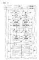
- Figure 1 is a schematic diagram of a portion of a data arithmetic unit in accordance with the present invention.
- FIG. 1 shows a schematic diagram of a portion of a data arithmetic unit (DAU) 20 which may be part of an integrated circuit.
- the integrated circuit may be part of a transceiver in a communications system or a portion of a communications system such as a mobile digital cellular telephone.
- DAU 20 is a portion of a processor 22 such as a microcontroller, microprocessor, or digital signal processor.
- DAU 20 includes a multiplexer 32 to select an input to a first input register 34 from a plurality of inputs.
- Input register 34 may be segmented into high and low portions represented as xh and xl. The high and low portions typically each contain n bits, where n is an arbitrary number. In a preferred embodiment, n is sixteen.
- First input register 34 is a 2n-bit register having high and low portions. An n-bit word can be multiplexed into each of the high portion, xh and low portion, xl. The expression 2n-bit is intended to be twice a word length n bits plus appropriate guard bits.
- DAU 20 includes at least two multiply-accumulate paths. Multipler 24 and adder 26 provide a first multiply-accumulate path; multiplier 28 and adder 30 provide a second multiply-accumulate path. Multiplexer 32 may have inputs coupled to a first databus 16, also designated the X databus, and a feedback path 36 from the output of adders 26 and 30. Multiplexer 38 selects an input from the plurality of inputs as an input to second input register 40, also designated the y register.
- Second input register 40 may be segmented into high and low portions represented as yh and yl. The high and low portions typically each contain n bits. Similarly, second input register 40 is a 2n-bit register having high and low portions. Multiplexer 38 may be coupled to a second databus 18, also designated the Y databus, and feedback path 36 from the output of adders 26 and 30.
- the bits from xh and xl portions of first input register 34 as well as the bits from yh and yl portions of second input register 40 are independently available to each multiplier 24 and 28 by way of crossover multiplexer 42.
- Crossover multiplexer 42 provides two inputs to each multiplier 24 and 28.
- Inputs 44 and 46 are provided to multiplier 24; inputs 48 and 50 are provided to multiplier 28.
- An n-bit word can be multiplexed into each of the high half and low half of each of registers 34 and 40.
- the output from either the high half or low half of either first input register 34 or second input register 40 can provide any of the inputs 44, 46, 48 or 50 to multipliers 24 and 28 through crossover multiplexer 42.
- Each multiplier 24 and 28 multiplies the inputs it receives and provides a product output.
- the product output from multiplier 24 is stored in a first product register 52, and is provided as an input to both multiplexers 56 and 58.
- the product output from multiplier 28 is stored in a second product register 54, and is provided as an input to both multiplexer 56 and multiplexer 58.
- Multiplexers 56 and 58 also have available as an input the contents of second input register 40.
- Accumulator file 62 is comprised of a plurality of registers 64. Registers 64 comprising accumulator file 62 are also 2n-bit registers accessible by high and low portions. The output of accumulator file 62 is coupled by line 66 as an input to multiplexer 56 and adder 26, and by line 68 as an input to multiplexer 58 and adder 30.
- the output of multiplexer 56 provides an input to adder 26.
- the sum output from adder 26 is passed through saturation block 70 to limit the output to an extremum value during overflow, and coupled as an input to multiplexers 32, 38 and 60.
- the output of multiplexer 58 provides an input to adder 30.
- the sum output from adder 30 is passed through saturation block 72 to limit the output to an extremum value during overflow, and is coupled as an input to multiplexers 32, 38 and 60.
- Multiplexer 60 can provide the output of either adder 26 or 30 to any of registers 64 in accumulator file 62.
- the select inputs to the various multiplexers are set by an instruction decoder in a control section of the processor architecture, not shown, to choose the appropriate input as an output.
- adder 30 is a three-input adder, and adder 26 has at least two inputs. Each of adders 26 and 30 provide a sum output that is a combination of the adder inputs.
- either or both adders may be split adders. Split adders can perform two additions or two subtractions such as by combining the high order bits of two operands and the low order bits of two operands. While adder 26 has been characterized as an adder, adder 26 can be an arithmetic logic unit capable of performing logical operations as well as addition and subtraction operations.
- Adder 26 may receive one of its inputs from the output of either multiplier 24 or multiplier 28 by way of product register 52 and 54 and multiplexer 56.
- adder 30 may receive one or two inputs from the outputs of multiplier 24 and multiplier 28 by way of product register 52 and 54, and in the case of the output from multiplier 24, multiplexer 58.
- the output of multiplier 24 in the first data path can be provided as an input to either adder 26 in the first data path or adder 30 in the second data path, or both.
- the output from multiplier 28 in the second data path can be provided as an input to adder 30 in the second data path or adder 26 in the first data path, or both.
- Two inputs to adder 26 may be provided as outputs from registers 64 of accumulator file 62 by way of line 66. While one input to adder 26 may be provided directly from the output of register file 62, another input may be provided through multiplexer 56. Similarly, two inputs to adder 30 may be provided as outputs from registers 64 of accumulator file 62 by way of 68. While one input to adder may be coupled directly to the output of register 64 of accumulator file 62, a second input to adder 30 is coupled through multiplexer 58 by way of line 68.
- Having at least one 3-input adder in a data path provides the opportunity for the user to compute two taps of a finite impulse response filter, or one tap of two independent filters. Furthermore, providing at least one of the two adders as a split adder provides additional flexibility that can further enhance performance. With at least one of the adders being a split adder, it is possible to perform up to three addition or subtraction operations in a single clock cycle. With both adders being split adders, it is possible to perform up to four addition or subtraction operations in a single clock cycle.
Landscapes
- Engineering & Computer Science (AREA)
- Physics & Mathematics (AREA)
- General Physics & Mathematics (AREA)
- Theoretical Computer Science (AREA)
- Computational Mathematics (AREA)
- Computing Systems (AREA)
- Mathematical Analysis (AREA)
- Mathematical Optimization (AREA)
- Pure & Applied Mathematics (AREA)
- General Engineering & Computer Science (AREA)
- Complex Calculations (AREA)
Abstract
There is disclosed a processor including at least two multiply-accumulate
data paths (24, 26; 28, 30). Each multiply-accumulate data path has at
least one multiplier (24 or 28) and at least one adder (26 or 30). At least one of the
adders (30) in at least one of the multiply-accumulate data paths is a three-input
adder.
Description
- This invention relates generally to multiple data path processors, and particularly to a multiple data path processor having a three-input adder.
- Multiple data path processors, such as multiple multiply-accumulate digital signal processors, are known. Such digital signal processors are used for executing algorithms to process digitized representations of signals using numerical operations such as, for example, in communications and video applications. Many multiple multiply-accumulate processors are designed to accumulate products using multiple, two-input arithmetic logic units. When filtering a signal such as in a finite impulse response filter algorithm, two-input arithmetic logic units limit the ability to maximize processor performance by requiring that the programmer structure the computations around the hardware limitations.
- What is needed is a multiply-accumulate data path that provides a more efficient technique for signal processing, such as calculating individual output samples of a finite impulse response filter.
- In accordance with the invention, a processor includes at least two multiply-accumulate data paths. Each multiply-accumulate data path has at least one multiplier and at least one adder. At least one of the adders in at least one of the multiply-accumulate data paths is a three-input adder.
- Figure 1 is a schematic diagram of a portion of a data arithmetic unit in accordance with the present invention.
- Figure 1 shows a schematic diagram of a portion of a data arithmetic unit (DAU) 20 which may be part of an integrated circuit. The integrated circuit may be part of a transceiver in a communications system or a portion of a communications system such as a mobile digital cellular telephone. DAU 20 is a portion of a processor 22 such as a microcontroller, microprocessor, or digital signal processor. DAU 20 includes a
multiplexer 32 to select an input to afirst input register 34 from a plurality of inputs.Input register 34 may be segmented into high and low portions represented as xh and xl. The high and low portions typically each contain n bits, where n is an arbitrary number. In a preferred embodiment, n is sixteen.First input register 34 is a 2n-bit register having high and low portions. An n-bit word can be multiplexed into each of the high portion, xh and low portion, xl. The expression 2n-bit is intended to be twice a word length n bits plus appropriate guard bits.DAU 20 includes at least two multiply-accumulate paths.Multipler 24 andadder 26 provide a first multiply-accumulate path;multiplier 28 andadder 30 provide a second multiply-accumulate path.Multiplexer 32 may have inputs coupled to afirst databus 16, also designated the X databus, and afeedback path 36 from the output ofadders second databus 18, also designated the Y databus, andfeedback path 36 from the output ofadders - The bits from xh and xl portions of
first input register 34 as well as the bits from yh and yl portions of second input register 40 are independently available to eachmultiplier crossover multiplexer 42.Crossover multiplexer 42 provides two inputs to eachmultiplier Inputs 44 and 46 are provided to multiplier 24;inputs registers 34 and 40. The output from either the high half or low half of eitherfirst input register 34 or second input register 40 can provide any of theinputs crossover multiplexer 42. Eachmultiplier multiplier 24 is stored in a first product register 52, and is provided as an input to bothmultiplexers 56 and 58. Similarly, the product output frommultiplier 28 is stored in asecond product register 54, and is provided as an input to both multiplexer 56 andmultiplexer 58.Multiplexers 56 and 58 also have available as an input the contents of second input register 40. -
Accumulator file 62 is comprised of a plurality ofregisters 64.Registers 64 comprisingaccumulator file 62 are also 2n-bit registers accessible by high and low portions. The output ofaccumulator file 62 is coupled by line 66 as an input to multiplexer 56 and adder 26, and by line 68 as an input tomultiplexer 58 and adder 30. - The output of multiplexer 56 provides an input to adder 26. The sum output from
adder 26 is passed throughsaturation block 70 to limit the output to an extremum value during overflow, and coupled as an input tomultiplexers multiplexer 58 provides an input to adder 30. The sum output fromadder 30 is passed through saturation block 72 to limit the output to an extremum value during overflow, and is coupled as an input tomultiplexers Multiplexer 60 can provide the output of eitheradder registers 64 inaccumulator file 62. - The select inputs to the various multiplexers are set by an instruction decoder in a control section of the processor architecture, not shown, to choose the appropriate input as an output.
- In a preferred embodiment,
adder 30 is a three-input adder, andadder 26 has at least two inputs. Each ofadders adder 26 has been characterized as an adder,adder 26 can be an arithmetic logic unit capable of performing logical operations as well as addition and subtraction operations. -
Adder 26 may receive one of its inputs from the output of either multiplier 24 or multiplier 28 by way ofproduct register 52 and 54 and multiplexer 56. Similarly,adder 30 may receive one or two inputs from the outputs ofmultiplier 24 and multiplier 28 by way ofproduct register 52 and 54, and in the case of the output frommultiplier 24,multiplexer 58. In this manner, the output ofmultiplier 24 in the first data path can be provided as an input to either adder 26 in the first data path or adder 30 in the second data path, or both. Similarly, the output frommultiplier 28 in the second data path can be provided as an input to adder 30 in the second data path oradder 26 in the first data path, or both. - Two inputs to adder 26 may be provided as outputs from
registers 64 ofaccumulator file 62 by way of line 66. While one input toadder 26 may be provided directly from the output ofregister file 62, another input may be provided through multiplexer 56. Similarly, two inputs to adder 30 may be provided as outputs fromregisters 64 ofaccumulator file 62 by way of 68. While one input to adder may be coupled directly to the output ofregister 64 ofaccumulator file 62, a second input toadder 30 is coupled throughmultiplexer 58 by way of line 68. - Having at least one 3-input adder in a data path provides the opportunity for the user to compute two taps of a finite impulse response filter, or one tap of two independent filters. Furthermore, providing at least one of the two adders as a split adder provides additional flexibility that can further enhance performance. With at least one of the adders being a split adder, it is possible to perform up to three addition or subtraction operations in a single clock cycle. With both adders being split adders, it is possible to perform up to four addition or subtraction operations in a single clock cycle.
Claims (35)
- A processor circuit including
a data arithmetic unit (20) having at least two multiply-accumulate data paths (24, 26; 28, 30), each multiply-accumulate data path having at least one multiplier (24 or 28) and at least one adder (26 or 30), the processor characterized in that at least one of the adders (30) being a three-input adder. - A processor as recited in claim 1, further characterized in that in each data path, an output from the multiplier (24; 28) is adapted to be coupled as an input to the adder.
- A processor as recited in claim 1, further characterized by a register file (62) for receiving an output from the at least one adder in each of the at least two data paths.
- A processor as recited in claim 1 further characterized in that at least one of the adders (26 or 30) is a split adder.
- A processor as recited in claim 1, further characterized in that an adder (26; 30) in each data path is a split adder.
- A processor as recited in claim 1, wherein a first data path includes a first multiplier (24) adapted to receive first and second inputs, the first multiplier adapted to provide an output that is a product of the first (44) and second (46) inputs, and a first adder (26) having at least two inputs, a first input of said at least two inputs adapted to be coupled to the output of the first multiplier, the first adder providing a first sum output that is a combination of the first adder inputs, and a second data path includes a second multiplier (28) adapted to receive third (48) and fourth (50) inputs, the second multiplier (28) adapted to provide an output that is a product of the third and fourth inputs and a second adder, the second adder providing a second sum output that is a combination of the second adder inputs the processor characterized by the second adder (30) being adapted to receive three inputs, a first input to the second adder adapted to be coupled to the output of the second multiplier.
- A processor as recited in claim 6, further characterized by a register file (62) adapted to be coupled to receive the first sum output from the first adder (26) and the second sum output from the second adder (30).
- A processor as recited in claim 7, further characterized by an input (44 or 46) to the first adder (24) is adapted to be coupled to receive outputs from the register file (62).
- A processor as recited in claim 7, further characterized by a second input to the second adder is adapted to be coupled (66) to receive outputs from the register file (62).
- A processor as recited in claim 6, further characterized by the output from the first multiplier is adapted to be coupled as an input to both the first adder (26) and the second adder (30).
- A processor as recited in claim 6, further characterized by the output from the second multiplier (28) is adapted to be coupled as an input to both the first adder (26) and the second adder.
- A processor, as recited in claim 10, further characterized by the output from the second multiplier (28) is adapted to be coupled as an input to both the first adder (26) and the second adder (30).
- A processor as recited in claim 6, further characterized by an input to one of said first and second multipliers (24 or 28) is adapted to be coupled as an input to the first adder (26).
- A processor as recited in claim 6, further characterized by an input to one of said first and second multipliers (24 or 28) is adapted to be coupled as an input to the second adder (30).
- A processor as recited in claim 6, further characterized by an input to one of said first and second multipliers (24 or 28) is adapted to be coupled as an input to both the first (26) and second adders (28).
- A processor as recited in claim 6, further characterized by the first sum output is adapted to be coupled as one of the first, second, third and fourth inputs.
- A processor as recited in claim 6, further characterized by the second sum output is adapted to be coupled as one of the first, second, third and fourth inputs.
- A processor as recited in claim 6, further characterized by the first sum output is adapted to be coupled as one of the first, second, third and fourth inputs, and the second sum output is adapted to be coupled as another one of the first, second, third and fourth inputs.
- A processor as recited in claim 6, further characterized by the first sum output is adapted to be coupled as two of the at least two inputs to the first adder (26).
- A processor as recited in claim 6, further characterized by the second sum output is adapted to be coupled as two of the inputs to the second adder (30).
- A processor as recited in claim 6, further characterized by the first sum output is adapted to be coupled as two of the inputs to the second adder (30).
- A processor as recited in claim 6, further charactered by the second sum output is adapted to be coupled as two of the at least two inputs to the first adder (26).
- A processor as recited in claim 6, further characterized by the processor is fabricated in an integrated circuit.
- A processor as recited in claim 6, further characterized by the processor is a digital signal processor.
- An integrated circuit including first and second multipliers, first and second adders, and first, second and third multiplexers, the integrated circuit characterized by the first multiplexer (42) adapted to receive first, second, third and fourth inputs, the first multiplexer adapted to provide the first, second, third and fourth inputs as outputs, the first multiplier (24) adapted to receive as inputs two of the first, second, third and fourth inputs, the first multiplier (24) adapted to provide an output that is a product of the two first multiplier inputs, the second multiplier (28) adapted to receive as inputs two of the first, second, third and fourth inputs, the first multiplier (28) adapted to provide an output that is a product of the two second multiplier inputs, the second multiplexer (56) adapted to receive as inputs an output from the first multiplier (24) and an output from the second multiplier (28), the second multiplexer adapted to provide one of the inputs as an output, the third multiplexer (58) adapted to receive as one of its inputs an output from the first multiplier the third multiplexer adapted to provide one of the inputs as an output, the first adder (26) having at least two inputs, a first input of said at least two inputs adapted to be coupled to the output of the second multiplexer (56), the first adder providing a first sum output that is a combination of the at least two inputs, and the second adder (30) adapted to receive at least three inputs, a first input adapted to be coupled to the output of the third multiplexer, the second adder providing a second sum that is a combination of the at least three inputs.
- An integrated circuit as recited in claim 25, characterized in that at least one of said first, second, third and fourth inputs to the first multiplexer (42) is also provided as an input to the second multiplexer (56).
- An integrated circuit as recited in claim 25, characterized in that at least one of said first, second, third and fourth inputs to the first multiplexer (42) is also provided as an input to the third multiplexer (58).
- An integrated circuit as recited in claim 25, characterized in that at least one of said first, second, third and fourth inputs to the first multiplexer (42) is also provided as an input to the both the second and third multiplexers (56, 58).
- An integrated circuit as recited in claim 25, characterized in that an accumulator file (62) of registers (64), the accumulator file (62) adapted to receive and store outputs from the first (26) and second (30) adders, the accumulator file (62) adapted to provide outputs.
- An integrated circuit as recited in claim 29, characterized in that an output from the register file (62) provides an input to the first adder (26).
- An integrated circuit as recited in claim 29, characterized in that an output from the register file (62) provides an input to the second multiplexer (56).
- An integrated circuit as recited in claim 29, characterized in that an output from the register file (62) provides an input to the second adder (30).
- An integrated circuit as recited in claim 29, characterized in that an output from the register file provides an input to the third multiplexer.
- An integrated circuit as recited in claim 29, further characterized in that a fourth multiplexer (60), the fourth multiplexer adapted to receive as inputs the outputs from the first (26) and second (30) adders, the fourth multiplexer (60) adapted to provide as an output the outputs from the first (26) and second (30) adders to the registers (64) in the accumulator file (62).
- An integrated circuit as recited in claim 34, characterized in that at least one of said first, second, third and fourth inputs to the first multiplexer (42) is an output from the fourth multiplexer (60).
Applications Claiming Priority (2)
| Application Number | Priority Date | Filing Date | Title |
|---|---|---|---|
| US97846897A | 1997-11-25 | 1997-11-25 | |
| US978468 | 1997-11-25 |
Publications (1)
| Publication Number | Publication Date |
|---|---|
| EP0919910A1 true EP0919910A1 (en) | 1999-06-02 |
Family
ID=25526118
Family Applications (1)
| Application Number | Title | Priority Date | Filing Date |
|---|---|---|---|
| EP98309404A Withdrawn EP0919910A1 (en) | 1997-11-25 | 1998-11-17 | Multiple data path processor with a three-input adder |
Country Status (3)
| Country | Link |
|---|---|
| EP (1) | EP0919910A1 (en) |
| JP (1) | JPH11259272A (en) |
| TW (1) | TW405087B (en) |
Citations (5)
| Publication number | Priority date | Publication date | Assignee | Title |
|---|---|---|---|---|
| EP0530936A1 (en) * | 1991-09-05 | 1993-03-10 | Cyrix Corporation | Method and apparatus for performing prescaled division |
| EP0615199A1 (en) * | 1993-03-11 | 1994-09-14 | Integrated Information Technology, Inc., | Video compression/decompression using discrete cosine transformation |
| EP0660245A2 (en) * | 1993-12-20 | 1995-06-28 | Motorola, Inc. | Arithmetic engine |
| GB2319152A (en) * | 1996-11-06 | 1998-05-13 | Hyundai Electronics Ind | An adaptive equalizer with a filter input circuit using a ring of flip-flops |
| WO1998035301A2 (en) * | 1997-02-07 | 1998-08-13 | Cirrus Logic, Inc. | Circuits, system, and methods for processing multiple data streams |
-
1998
- 1998-11-17 EP EP98309404A patent/EP0919910A1/en not_active Withdrawn
- 1998-11-18 TW TW87119094A patent/TW405087B/en not_active IP Right Cessation
- 1998-11-25 JP JP10333783A patent/JPH11259272A/en active Pending
Patent Citations (5)
| Publication number | Priority date | Publication date | Assignee | Title |
|---|---|---|---|---|
| EP0530936A1 (en) * | 1991-09-05 | 1993-03-10 | Cyrix Corporation | Method and apparatus for performing prescaled division |
| EP0615199A1 (en) * | 1993-03-11 | 1994-09-14 | Integrated Information Technology, Inc., | Video compression/decompression using discrete cosine transformation |
| EP0660245A2 (en) * | 1993-12-20 | 1995-06-28 | Motorola, Inc. | Arithmetic engine |
| GB2319152A (en) * | 1996-11-06 | 1998-05-13 | Hyundai Electronics Ind | An adaptive equalizer with a filter input circuit using a ring of flip-flops |
| WO1998035301A2 (en) * | 1997-02-07 | 1998-08-13 | Cirrus Logic, Inc. | Circuits, system, and methods for processing multiple data streams |
Also Published As
| Publication number | Publication date |
|---|---|
| JPH11259272A (en) | 1999-09-24 |
| TW405087B (en) | 2000-09-11 |
Similar Documents
| Publication | Publication Date | Title |
|---|---|---|
| EP0901068B1 (en) | Near-orthogonal dual-mac instruction set architecture with minimal encoding bits | |
| US6009451A (en) | Method for generating barrel shifter result flags directly from input data | |
| US6286024B1 (en) | High-efficiency multiplier and multiplying method | |
| EP1623307B1 (en) | Processor reduction unit for accumulation of multiple operands with or without saturation | |
| EP0657804B1 (en) | Overflow control for arithmetic operations | |
| US20120278590A1 (en) | Reconfigurable processing system and method | |
| EP0577101B1 (en) | Multiplier accumulator | |
| JPH10187438A (en) | Method for reducing transition to input of multiplier | |
| US5721696A (en) | Method and system for performing an FIR filtering operation | |
| EP1049025A1 (en) | Method and apparatus for arithmetic operation | |
| US5657263A (en) | Computer processor having a pipelined architecture which utilizes feedback and method of using same | |
| US5771391A (en) | Computer processor having a pipelined architecture and method of using same | |
| US6675286B1 (en) | Multimedia instruction set for wide data paths | |
| KR19980041758A (en) | 2-Bit Booth Multiplier with Reduced Data Path Width | |
| EP1116101B1 (en) | Arithmetic unit with, and method of selectively delaying a multiplication result | |
| US5936871A (en) | Method and system for performing an L2 norm operation | |
| EP1052568B1 (en) | Three input split-adder | |
| US5951628A (en) | Method and system for performing a convolution operation | |
| EP0919910A1 (en) | Multiple data path processor with a three-input adder | |
| JP3579087B2 (en) | Arithmetic unit and microprocessor | |
| EP0380099B1 (en) | Register and arithmetic logic unit | |
| US5696986A (en) | Computer processor utilizing logarithmic conversion and method of use thereof | |
| US5822609A (en) | Processing circuit for performing a convolution computation | |
| JP3252954B2 (en) | Multiplication method and multiplication circuit | |
| US20030233384A1 (en) | Arithmetic apparatus for performing high speed multiplication and addition operations |
Legal Events
| Date | Code | Title | Description |
|---|---|---|---|
| PUAI | Public reference made under article 153(3) epc to a published international application that has entered the european phase |
Free format text: ORIGINAL CODE: 0009012 |
|
| AK | Designated contracting states |
Kind code of ref document: A1 Designated state(s): DE FR |
|
| AX | Request for extension of the european patent |
Free format text: AL;LT;LV;MK;RO;SI |
|
| 17P | Request for examination filed |
Effective date: 19991119 |
|
| AKX | Designation fees paid |
Free format text: DE |
|
| RBV | Designated contracting states (corrected) |
Designated state(s): DE FR |
|
| 17Q | First examination report despatched |
Effective date: 20020604 |
|
| STAA | Information on the status of an ep patent application or granted ep patent |
Free format text: STATUS: THE APPLICATION IS DEEMED TO BE WITHDRAWN |
|
| 18D | Application deemed to be withdrawn |
Effective date: 20021015 |