EP0910031A2 - Information card system - Google Patents
Information card system Download PDFInfo
- Publication number
- EP0910031A2 EP0910031A2 EP98124871A EP98124871A EP0910031A2 EP 0910031 A2 EP0910031 A2 EP 0910031A2 EP 98124871 A EP98124871 A EP 98124871A EP 98124871 A EP98124871 A EP 98124871A EP 0910031 A2 EP0910031 A2 EP 0910031A2
- Authority
- EP
- European Patent Office
- Prior art keywords
- information
- signal
- information card
- card
- coil
- Prior art date
- Legal status (The legal status is an assumption and is not a legal conclusion. Google has not performed a legal analysis and makes no representation as to the accuracy of the status listed.)
- Withdrawn
Links
Images


Classifications
-
- G—PHYSICS
- G06—COMPUTING; CALCULATING OR COUNTING
- G06K—GRAPHICAL DATA READING; PRESENTATION OF DATA; RECORD CARRIERS; HANDLING RECORD CARRIERS
- G06K19/00—Record carriers for use with machines and with at least a part designed to carry digital markings
- G06K19/06—Record carriers for use with machines and with at least a part designed to carry digital markings characterised by the kind of the digital marking, e.g. shape, nature, code
-
- G—PHYSICS
- G06—COMPUTING; CALCULATING OR COUNTING
- G06K—GRAPHICAL DATA READING; PRESENTATION OF DATA; RECORD CARRIERS; HANDLING RECORD CARRIERS
- G06K7/00—Methods or arrangements for sensing record carriers, e.g. for reading patterns
- G06K7/10—Methods or arrangements for sensing record carriers, e.g. for reading patterns by electromagnetic radiation, e.g. optical sensing; by corpuscular radiation
- G06K7/10009—Methods or arrangements for sensing record carriers, e.g. for reading patterns by electromagnetic radiation, e.g. optical sensing; by corpuscular radiation sensing by radiation using wavelengths larger than 0.1 mm, e.g. radio-waves or microwaves
- G06K7/10316—Methods or arrangements for sensing record carriers, e.g. for reading patterns by electromagnetic radiation, e.g. optical sensing; by corpuscular radiation sensing by radiation using wavelengths larger than 0.1 mm, e.g. radio-waves or microwaves using at least one antenna particularly designed for interrogating the wireless record carriers
- G06K7/10326—Methods or arrangements for sensing record carriers, e.g. for reading patterns by electromagnetic radiation, e.g. optical sensing; by corpuscular radiation sensing by radiation using wavelengths larger than 0.1 mm, e.g. radio-waves or microwaves using at least one antenna particularly designed for interrogating the wireless record carriers the antenna being of the very-near field type, e.g. capacitive
Definitions
- the present invention relates to an information card system and particularly relates to an information card system which writes information in a non-contact manner.
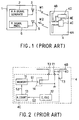
- FIG. 1 An example of the conventional information card reader which reads information of an information card is illustrated in FIG. 1.
- a response requiring signal W1 using a microwave of 2.45 GHz, for example, as a carrier is generated in a response requiring signal generating circuit 2 and is emitted from a transmission antenna 3 to an information card 4.
- a response information signal W2 which is returned from the information card 4 is received in a response signal processing circuit 6 through a receiving antenna 5.
- the information card reading system may be used for checking visitors, who have no information card 4 as an identification card or checking freight with the information card 4 as a tag.
- Japanese Patent (unexamined) Laid-open No. 1(1989)-182782 proposes the information card 4 which is used in such an information card reading systems.
- a dipole antenna 4B, an information signal generating circuit 4C and a power supply battery 4D are connected by a wiring pattern 4E.
- the dipole antenna 4B is mounted on the wiring board 4A to form part of the wiring pattern, and the information signal generating circuit 4C has an integrated circuit (IC) structure.
- the dipole antenna 4B changes in the reflection ratio to the carrier, emitted as a response requiring signal W1 from the information reader 1, by changing impedance at feeding point thereof according to an information signal generated in the information signal generating circuit 4C, and thereby the reflected wave is returned as a response information signal W2.
- the information signal generating circuit 4C has an electric circuit configuration as shown in FIG. 2.
- Information data S1 previously stored in an information memory 11, a PROM for example, is read according to an address signal S3 of an address counter 13 which is actuated by a clock signal S2 of a clock signal generator 12, and the information data read is supplied to an variable impedance circuit 14 which is made of a field effect transistor.
- the variable impedance circuit 14 is interconnected between a pair of feeding point terminals T1 and T2, and the dipole antenna 4B is connected to the feeding point terminals T1 and T2.
- impedance of the dipole antenna 4B at the feeding point is variable controlled by performing on-off actuation of the field effect transistor when the information data S1 has logic "1" or "0", and thereby the reflection ratio to the response requiring signal W1 incident upon the dipole antenna 4B is variable controlled.
- a power supply battery 4D Interconnected between the earth side feeding point terminal T1 and a power supply terminal T3 of the information signal generating circuit 4C is a power supply battery 4D. This enables the impedance variable control at the feeding point of the dipole antenna 4B to be always continuously performed by the information data S1.
- a specific identification code is allotted to the information memory 11 of each information card 4, and hence information contained in information cards 4 is positively read by the information reader 1.
- an object of the present invention to provide an information card system which is capable of writing information in the information card in a non-contact manner with excellent facility.
- the present invention provides an information card system comprising an information card storing information data therein and capable of receiving a signal from a card reader, transforming the signal in response to the information data and transmitting the transformed signal back to the card reader, and an information writer.
- the information card includes a pair of electrode plate means for receiving the information data, and means for storing said information data;
- the information writer includes information data generating means for generating the information data, and a pair of writing electrode plate means supplied with the information data and for generating an electrical field in cooperative with the pair of electrode plate means when the information card is moved toward the information writer, thereby the information data being written in the information card without any contact between the information card and the information writer.
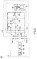
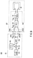
- the information card system 20 includes an information card 22 and an information writer 21 for writing information in the information card 22.
- a write signal generating circuit 23 produces a write information signal S W according to a predetermined information data and sends it as a baseband signal to writing electrodes 25A and 25B through an amplifying circuit 24.
- a change in voltage is produced between the writing electrodes 25A and 25B in response to the write information signal S W .
- the information card 22 includes a printed wiring board 4A which mounts a plate 27, a power supply battery 29 and an integrated circuit 30 on it.
- the plate 27 and the power supply battery 29 are connected to the integrated circuit 30 through a wiring pattern, and the information card 22 is sealed at the front with a sealing sheet material.
- the power supply battery 29 is a so-called paper battery in the shape of a rectangular thin sheet 20 mm wide and 30 mm long, and the power supply battery 29 has a front electrode surface 29A as a positive electrode and a rear electrode surface 29B as a negative electrode.
- the plate 27 is in the shape of a rectangle 8 mm wide and 15 mm long and constitutes part of the wiring pattern.
- the plate 27 and the power supply battery 29 are provided on the front of the information card 22 at the same level so that the plate 27 and the power supply battery 29 oppositely face the writing electrodes 25A and 25B respectively when the information card 22 is placed in the vicinity of the information writer 21.
- the electrode surface 29B and the plate 27 are used as plates for inputting data.
- the writing electrodes 25A and 25B of the information writer 21 and the plate 27 and the electrode surface 29B of the information card 22 may produce electric fields respectively.
- an electric field is generated by a write information signal S W which is inputted to the writing electrode 25A with a reference potential of the writing electrode 25B, so that an input information signal S IN is produced at the plate 27 in response to the write information signal S W with a reference potential of the electrode surface 29B.
- the write information signal S W is transmitted to the information card 22 as the input information signal S IN in a non-contact fashion.
- the input information signal S IN is, as shown in FIG. 3, inputted to an amplifier circuit 40 of a complementary MOS through a clipper 35 and a current limiting circuit 37.
- the clipper 35 includes diodes 33 and 34 while the current limiting circuit 37 contains a resistance R1 and a diode 36.
- the input information signal S IN is amplified by the amplifier circuit 40 with the power supply battery 29 and is then sent as an input write signal S INW to an information signal processing circuit 41 for storing as an information data.
- the write information signal S W is sent from the information writer 21 to the information card 22 in the non-contact manner and is stored in the information card 22 as information data.
- the electrode pattern 31 is connected through a wiring pattern to an information signal generating circuit 4C (FIG. 2) arranged within the information signal processing circuit 41.
- the electrode pattern 31 changes in impedance in response to an information data from the information signal generating circuit 4C.
- An induction electric field is produced by placing the electrode pattern 31 close to an information reading coil of an information reader (not shown), and thereby the information data from the information signal generating circuit 4C is transmitted to the information reader in a non-contact manner.
- the electrode pattern 31 is formed with a length of one wavelength of a microwave, and hence the electrode pattern 31 reflects a response requiring signal W1 (FIG. 1) which is sent from the information reader with the microwave as a carrier, at a predetermined reflection coefficient to thereby send a response information signal W2.
- W1 response requiring signal
- the information data of the information signal generating circuit 4C is sent in the non-contact manner using microwave.
- information data stored in the information card 22 are read by the proximity information reader according to inductive coupling.
- a remote information reader such as the information reader 1 in FIG. 1 can read the information data of the information card 22.
- the information card 22 may be built as a proximity read card or a remote read card according to the need.
- the information card 22 is brought close to the information writer 21 so that the writing electrodes 25A and 25B are placed at an interval of several mm from the plate 27 and the electrode surface 29B, respectively.
- the write information signal S W from the write signal generating circuit 23 is sufficiently amplified through the amplifying circuit 24, and electric fields are produced between the writing electrode 25A and the plate 27 and between the writing electrode 25B and the electrode surface 29B.
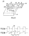
- the write information signal S W shown in FIG. 5A is inputted to the plate 27 of the information card 22 in the non-contact manner using static coupling.
- the cathode of the diode 33 of the clipper 35 is maintained at a supply voltage V CC since the cathode is connected to the positive electrode of the power supply battery 29.
- the anode of the diode 34 is held at the reference voltage, and when the input information signal S IN drops below the reference voltage, the diode 34 is hence turned on, so that the amplitude of the input information signal S IN is also limited in the low level side.
- the input information signal S IN is thus limited in amplitude to a predetermined signal level and is subsequently limited in current by the resistance R1 and the diode 36 of the current limiting circuit 37. Then, the input information signal S IN is inputted to the amplifier circuit 40, from which the input write signal S INW is sent to the information signal processing circuit 41, where the signal undergoes a predetermined signal processing and is then stored in the memory. In this manner, the amplifier circuit 40 and the information signal processing circuit 41 are protected even if the input information signal S IN is inputted at an excessively large signal level. Thus, the write information signal S W from the information writer 21 is positively written in the information card 22 in a non-contact manner.
- the input write signal S INW according to the write information signal S W is positively written in the information card 22 in the non-contact fashion in the following manners: electric fields are produced between the writing electrode 25A and the plate 27 and between the writing electrode 25B and the electrode surface 29B; the information signal S W is amplified by the amplifying circuit 24 of the information writer 21 to produce the input information signal S IN at a signal level required for the static coupling; the input information signal S IN is limited in amplitude by the clipper 35 of the information card 22; and the input information signal S IN is limited in current by the current limiting circuit 37.
- the negative electrode surface 29B of the power supply battery 29 is used as a signal input electrode plate, and thereby the wiring board 4A is fairly effectively used in space. This enables the information card 22 to be miniaturized.
- the information card 22 uses the 8 mm x 15 mm rectangular plate 27 and the 20 mm x 30 mm rectangular electrode surface 29B, but the plate 27 and the electrode surface 29B may have various sizes and configurations.
- the writing electrodes 25A and 25B of the information writer 21 are changed in configuration and size.
- information is written in the information card 22 by static coupling, but the present invention is not limited to this.
- Remote writing of information in the information card 22 using microwave may be achieved by forming the plate 27 and the electrode surface 29B to each have a length equal to half the wavelength of the microwave.
- the information of the information card 22 of the embodiment is read by both a proximity information reader and a remote information reader.
- the former reads information from the information card 22 by the electrode pattern 31 according to inductive coupling, and the latter use microwave.
- the information card 22 may be only for the proximity information reader or the remote information reader.
- FIGS. 6 and 7 another embodiment of the present invention will be described.
- parts corresponding to the parts of FIGS. 3 and 4 are designated by the same reference numerals.
- the information writer 21 of FIG. 6 is identical in construction as the information writer 21 in FIG. 3, and the description thereof is hence omitted.
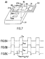
- the information card 22 has plates 27A and 27B and a loop-shaped electrode pattern 31 mounted on a printed wiring board 4A.
- the plates 27A and 27B and the electrode pattern 31 are connected to the integrated circuit 30 to form parts of a wiring pattern, and the information card 22 is sealed at the front with a sealing sheet.
- a plate 28 is provided to oppositely face the upper surfaces of the plates 27A and 27B at predetermined intervals for adding capacity.
- the plate 28 is formed to cover the plates 27A and 27B.
- An insulating film, such as a paper, is placed between the plate 28 and the plates 27A and 27B to keep a predetermined interval for providing predetermined capacities, respectively.
- the plates 27A and 27B are in the shape of a rectangle about 8 mm wide and about 15 mm long.
- the plates 27A and 27B oppositely face the writing electrodes 25A and 25B respectively when the information card 22 is placed in the vicinity of the information writer 21.
- the plates 27A and 27B are used as electrode plates for inputting data.
- the writing electrodes 25A and 25B or the information writer 21 and the plates 27A and 27B may produce electric fields respectively.
- an electric field is generated by a write information signal S W which is inputted to the writing electrode 25A with a reference potential of the writing electrode 25B, so that an input information signal S IN2 is produced at the plate 27A in response to the write information signal S W with a reference potential of the plate 27B.
- the input information signal S IN2 is, as shown in FIG. 6, inputted to a clipper 35 including diodes 33 and 34.
- This clipper 35 operates in the same manner as the clipper 35 of FIG. 3, and the description thereof is hence omitted.
- the other construction of the information card 22 is the same as that of the information card 22 of the preceding embodiment, and the description thereof is also omitted.
- the information card 22 is brought close to the information writer 21 so that the writing electrodes 25A and 25B are placed at an interval of several mm from the plates 27A and 27B, respectively.
- the write information signal S W from the write signal generating circuit 23 is sufficiently amplified through the amplifying circuit 24, and electric fields are produced between the plate 27A and the writing electrode 25A and between the plate 27B and the writing electrode 25B.
- the write information signal S W shown in FIG. 8A, is inputted to the plate 27A of the information card 22 in the non-contact manner using static coupling.
- the plate 28 provides additional capacitances to the plates 27A and 27B.
- the time constant of the input capacitance 43 which is produced in the integrated circuit 30 increases by the additional capacitances of the plates 27A and 27B.
- an input information signal S IN2 is inputted to the amplifier circuit 40 in the waveform similar to the waveform of the write information signal S W without producing little waveform distortion as in FIG. 8C.
- the resultant input write signal S INW is sent to the information signal processing circuit 41, where the input write signal S INW undergoes the signal processing at a predetermined level of a threshold value and is then stored in the memory.
- the write information signal S W which has been sent from the information writer 21 is inputted to the information card 22 in a non-contact manner and is positively stored in it as an information data.
- the provision of the plate 28 to face the plates 27A and 27B for additional capacitance enables information data to be positively written in the information card 22 from the information writer 21 in the non-contact manner with little waveform distortion in the input information signal S IN2 .
- FIGS. 9 and 10 A third embodiment of the present invention will be described with reference to FIGS. 9 and 10.
- parts corresponding to parts of FIG. 3 are designated by the same reference numberals.
- an information writer 21 of an information card system 20 includes a write signal generating circuit 23 where a write information signal S W (FIG. 10A) is produced according to a predetermined information data, and the write information signal S W is sent as a baseband signal to a multiplier circuit 51 at a data transfer speed of 100 kbps, for example.
- a frequency generating circuit 50 inputs a reference frequency signal S F of a high frequency 100 MHz, for example, to the multiplier circuit 51, and thereby the reference frequency signal S F is amplitude modulated according to the write information signal S W to produce a modulated signal S EN1 (FIG. 10B), which is sent to writing electrodes 25A and 25B through an amplifying circuit 24.
- a modulated signal S EN1 FIG. 10B
- the information card of the structure shown in FIG. 4 may be used as the information card 22.
- an input modulated signal S EN2 is produced in a plate 29A in response to the modulated signal S EN1 , with a reference voltage of another plate 29B.
- the input modulated signal S EN2 is sent to a detector circuit 52 including a diode to perform envelope detection, so that as shown in FIG. 10C an input information signal S IN2 is produced in response to the write information signal S W .
- the input information signal S IN2 is transmitted to an information signal processing circuit 41 for predetermined signal processing and is then stored as an information data in a memory in the information signal processing circuit 41.
- the information card 22 of the third embodiment is identical in the other parts to the information card 22 of FIG. 3, and the description thereof is hence omitted.
- an information reader which reads data, saved in the manner above stated, will be described.
- an information card system 20 includes an information reader 121 and an information card 22.
- the information reader 121 is provided with a frequency generating circuit 125 which sends a reference signal S F of a predetermined frequency higher than several MHz to a magnetic field generating coil 128A through an amplifier circuit 126 of a TTL (transistor transistor logic) circuit configuration and a resistance R2.
- TTL transistor transistor logic
- the information reader 121 further includes a reading coil 128B arranged at a position opposing to the magnetic field generating coil 128A at a predetermined interval of several centimeters.
- a reading coil 128B arranged at a position opposing to the magnetic field generating coil 128A at a predetermined interval of several centimeters.
- the detection circuit 130 obtains a detected signal S EV by performing envelope detection at the signal level (voltage level) of the read signal S MV and sends it to a comparison circuit 133 through an amplifier circuit 131.
- the comparison circuit 133 converts the detected signal S EV to a binary signal S BI at a predetermined signal level and then transmits the binary signal S BI to a subsequent signal processing unit (not shown).
- the magnetic field generating coil 128A and the reading coil 128B are spaced, and the information card 22 is inserted in to the spacing.
- an electrode pattern 135 is attached to a wiring board 104A to substantially form a 30 mm x 37 mm rectangular loop.
- a field effect transistor 136 is connected to the electrode pattern 135 at opposite ends of the latter as feeding points.
- the electrode pattern 135, the field effect transistor 136, an information signal generating circuit 104C and a power supply battery 104D are connected through a wiring pattern.
- the field effect transistor 136 is on-off controlled according to an information signal sent from the information signal generating circuit 104C, and thereby the loop of the electrode pattern 135 is opened or closed.
- a reference signal S F of a frequency 20 MHz, for example, is inputted to the magnetic field generating coil 128A, current flowing in the magnetic field generating coil 128A changes in response to the reference signal S F , so that an induction field is generated between the magnetic field generating coil 128A and the reading coil 128B to produce an induced electromotive force in the reading coil 128B.
- the information card 22 is inserted into the space between the magnetic field generating coil 128A and the reading coil 128B to face the electrode pattern 135 of the information card 22 to the magnetic field generating coil 128A and reading coil 128B, and induced current thus flows in the electrode pattern 135 of the information card 22 only while the electrode pattern 135 is controlled to form a closed loop by turning on the field effect transistor 136.
- the electrode pattern 135 is controlled to form a closed loop by turning on the field effect transistor 136.
- the electromotive force induced in the reading coil 128B reduces, so that the signal level (amplitude) of the read signal S MV becomes smaller.
- This change in amplitude is detected by envelope detection in the detection circuit 130 and thereby a detected signal S EV which changes in signal level according to information data of the information card 22 is provided.
- a binary signal S BI which changes according to the information data of the information card 22 is obtained by converting the detected signal S EV to a binary signal in the comparison circuit 133.
- the binary signal S BI is sent to the subsequent signal processing unit to apply a predetermined signal processing, and thereby information data of the information card 22 can be read in a non-contact manner.
- Information data of the information card of FIG. 11 is positively read by detecting the detected signal S EV in the most sensitive condition by tuning the tuning capacitor C1.
- the loop of the electrode pattern 135 is opened or closed in response to information data of the information card 22, and thereby a change of the induction field between the magnetic field generating coil 128A and the reading coil 128B is detected on the side of the information reader 121, so that the information reader 121 reads information data of the information card 22 in the non-contact manner.
Landscapes
- Engineering & Computer Science (AREA)
- Physics & Mathematics (AREA)
- Health & Medical Sciences (AREA)
- Toxicology (AREA)
- General Physics & Mathematics (AREA)
- Theoretical Computer Science (AREA)
- Electromagnetism (AREA)
- General Health & Medical Sciences (AREA)
- Artificial Intelligence (AREA)
- Computer Vision & Pattern Recognition (AREA)
- Computer Networks & Wireless Communication (AREA)
- Credit Cards Or The Like (AREA)
- Financial Or Insurance-Related Operations Such As Payment And Settlement (AREA)
Abstract
Description
- The present invention relates to an information card system and particularly relates to an information card system which writes information in a non-contact manner.
- An example of the conventional information card reader which reads information of an information card is illustrated in FIG. 1. In the
information card reader 1, a response requiring signal W1 using a microwave of 2.45 GHz, for example, as a carrier is generated in a response requiringsignal generating circuit 2 and is emitted from atransmission antenna 3 to an information card 4. A response information signal W2 which is returned from the information card 4 is received in a responsesignal processing circuit 6 through a receivingantenna 5. In this manner, the information card reading system may be used for checking visitors, who have no information card 4 as an identification card or checking freight with the information card 4 as a tag. - Japanese Patent (unexamined) Laid-open No. 1(1989)-182782 proposes the information card 4 which is used in such an information card reading systems. In the information card 4, a
dipole antenna 4B, an information signal generatingcircuit 4C and apower supply battery 4D are connected by awiring pattern 4E. Thedipole antenna 4B is mounted on thewiring board 4A to form part of the wiring pattern, and the information signal generatingcircuit 4C has an integrated circuit (IC) structure. Thedipole antenna 4B changes in the reflection ratio to the carrier, emitted as a response requiring signal W1 from theinformation reader 1, by changing impedance at feeding point thereof according to an information signal generated in the information signal generatingcircuit 4C, and thereby the reflected wave is returned as a response information signal W2. - The information signal generating
circuit 4C has an electric circuit configuration as shown in FIG. 2. Information data S1 previously stored in aninformation memory 11, a PROM for example, is read according to an address signal S3 of anaddress counter 13 which is actuated by a clock signal S2 of aclock signal generator 12, and the information data read is supplied to anvariable impedance circuit 14 which is made of a field effect transistor. - The
variable impedance circuit 14 is interconnected between a pair of feeding point terminals T1 and T2, and thedipole antenna 4B is connected to the feeding point terminals T1 and T2. Thus, impedance of thedipole antenna 4B at the feeding point is variable controlled by performing on-off actuation of the field effect transistor when the information data S1 has logic "1" or "0", and thereby the reflection ratio to the response requiring signal W1 incident upon thedipole antenna 4B is variable controlled. - Interconnected between the earth side feeding point terminal T1 and a power supply terminal T3 of the information signal generating
circuit 4C is apower supply battery 4D. This enables the impedance variable control at the feeding point of thedipole antenna 4B to be always continuously performed by the information data S1. - A specific identification code is allotted to the
information memory 11 of each information card 4, and hence information contained in information cards 4 is positively read by theinformation reader 1. - To previously write information to the information card 4, it is proposed to bring electrodes of a writer into contact with electrodes of the information card 4. However, this method of writing information in the contact manner produces a problem that in mass production of the information card productivity is deteriorated due to the additional process of the direct contact.
- To overcome this problem there is proposed a method in which electrode plates are formed on an information card to send and receive information. The plates are placed in the vicinity of plates formed on a separate writer to produce an electric coupling between them for sending and receiving information in a non-contact manner (Japanese Patent (unexamined) Laid-open Publication 63(1988)-39396). However, in both writing information to and reading information from the information card, the information card must be placed in the vicinity of the information reader since the information card uses the plates for writing and reading information. Thus, the information card is not sufficient in the point of facility.
- Accordingly, it is an object of the present invention to provide an information card system which is capable of writing information in the information card in a non-contact manner with excellent facility.
- It is another object of the present invention to provide an information card system which is capable of previously preventing deterioration in input waveform when the input signal is inputted by an static coupling.
- It is still another object of the present invention to provide an information card system which is capable of reading data stored in an information card in a non-contact manner with a simple construction.
- In view of these and other objects, the present invention provides an information card system comprising an information card storing information data therein and capable of receiving a signal from a card reader, transforming the signal in response to the information data and transmitting the transformed signal back to the card reader, and an information writer. The information card includes a pair of electrode plate means for receiving the information data, and means for storing said information data; the information writer includes information data generating means for generating the information data, and a pair of writing electrode plate means supplied with the information data and for generating an electrical field in cooperative with the pair of electrode plate means when the information card is moved toward the information writer, thereby the information data being written in the information card without any contact between the information card and the information writer.
- In the drawings:
- FIG. 1 is a block diagram illustrating the conventional information card system;
- FIG. 2 is a block diagram showing in more detail the information signal generating circuit of FIG. 1;
- FIG. 3 is a block diagram showing an information card system in accordance with the first embodiment of the present invention;
- FIG. 4 is a perspective view of the information card system of FIG. 3;
- FIGS. 5A and 5B are waveform charts illustrating the operation of the information card system of FIG. 3;
- FIG. 6 is a block diagram showing an information card system in accordance with a second embodiment of the present invention;
- FIG. 7 is a perspective view of the information card system of FIG. 6;
- FIGS. 8A, 8B and 8C are waveform charts illustrating the operation of information card system of FIG. 6;
- FIG. 9 is a block diagram showing an information card system in accordance with a third embodiment of the present invention;
- FIGS. 10A to 10D are waveform charts illustrating the operation of information card system of FIG. 9; and
- FIG. 11 is a block diagram showing an information card reader of the present invention.
-
- Referring to FIGS. 3 and 4, an
information card system 20 of the present invention will be described. Theinformation card system 20 includes aninformation card 22 and aninformation writer 21 for writing information in theinformation card 22. In theinformation writer 21, a write signal generatingcircuit 23 produces a write information signal SW according to a predetermined information data and sends it as a baseband signal to writingelectrodes circuit 24. Thus, a change in voltage is produced between thewriting electrodes - As shown in FIG. 4, the
information card 22 includes a printedwiring board 4A which mounts aplate 27, apower supply battery 29 and an integratedcircuit 30 on it. Theplate 27 and thepower supply battery 29 are connected to the integratedcircuit 30 through a wiring pattern, and theinformation card 22 is sealed at the front with a sealing sheet material. - The
power supply battery 29 is a so-called paper battery in the shape of a rectangularthin sheet 20 mm wide and 30 mm long, and thepower supply battery 29 has afront electrode surface 29A as a positive electrode and arear electrode surface 29B as a negative electrode. - The
plate 27 is in the shape of a rectangle 8 mm wide and 15 mm long and constitutes part of the wiring pattern. Theplate 27 and thepower supply battery 29 are provided on the front of theinformation card 22 at the same level so that theplate 27 and thepower supply battery 29 oppositely face thewriting electrodes information card 22 is placed in the vicinity of theinformation writer 21. Thus, theelectrode surface 29B and theplate 27 are used as plates for inputting data. When theinformation card 22 is placed close to theinformation writer 21 at a predetermined interval, thewriting electrodes information writer 21 and theplate 27 and theelectrode surface 29B of theinformation card 22 may produce electric fields respectively. Thus, an electric field is generated by a write information signal SW which is inputted to thewriting electrode 25A with a reference potential of thewriting electrode 25B, so that an input information signal SIN is produced at theplate 27 in response to the write information signal SW with a reference potential of theelectrode surface 29B. In this manner, the write information signal SW is transmitted to theinformation card 22 as the input information signal SIN in a non-contact fashion. - The input information signal SIN is, as shown in FIG. 3, inputted to an
amplifier circuit 40 of a complementary MOS through aclipper 35 and a current limitingcircuit 37. Theclipper 35 includesdiodes 33 and 34 while the current limitingcircuit 37 contains a resistance R1 and adiode 36. The input information signal SIN is amplified by theamplifier circuit 40 with thepower supply battery 29 and is then sent as an input write signal SINW to an informationsignal processing circuit 41 for storing as an information data. Thus, the write information signal SW is sent from theinformation writer 21 to theinformation card 22 in the non-contact manner and is stored in theinformation card 22 as information data. - On the printed
wiring board 4A of theinformation card 22, there is mounted a loop-shaped electrode pattern 31 in addition to theplate 27 and thepower supply battery 29. Theelectrode pattern 31 is connected through a wiring pattern to an informationsignal generating circuit 4C (FIG. 2) arranged within the informationsignal processing circuit 41. - The
electrode pattern 31 changes in impedance in response to an information data from the informationsignal generating circuit 4C. An induction electric field is produced by placing theelectrode pattern 31 close to an information reading coil of an information reader (not shown), and thereby the information data from the informationsignal generating circuit 4C is transmitted to the information reader in a non-contact manner. Theelectrode pattern 31 is formed with a length of one wavelength of a microwave, and hence theelectrode pattern 31 reflects a response requiring signal W1 (FIG. 1) which is sent from the information reader with the microwave as a carrier, at a predetermined reflection coefficient to thereby send a response information signal W2. Thus, the information data of the informationsignal generating circuit 4C is sent in the non-contact manner using microwave. - In the
information card system 20, information data stored in theinformation card 22 are read by the proximity information reader according to inductive coupling. Moreover, a remote information reader such as theinformation reader 1 in FIG. 1 can read the information data of theinformation card 22. Theinformation card 22 may be built as a proximity read card or a remote read card according to the need. - To write the write information signal SW of the
information writer 21 to theinformation card 22, theinformation card 22 is brought close to theinformation writer 21 so that thewriting electrodes plate 27 and theelectrode surface 29B, respectively. In this event, the write information signal SW from the writesignal generating circuit 23 is sufficiently amplified through the amplifyingcircuit 24, and electric fields are produced between the writingelectrode 25A and theplate 27 and between the writingelectrode 25B and theelectrode surface 29B. Thus, the write information signal SW shown in FIG. 5A is inputted to theplate 27 of theinformation card 22 in the non-contact manner using static coupling. - In this event, the cathode of the
diode 33 of theclipper 35 is maintained at a supply voltage VCC since the cathode is connected to the positive electrode of thepower supply battery 29. When the input information signal SIN exceeds a voltage level VMAX which is equal to a forward direction operating voltage VF of thediode 33 added to the supply voltage VCC of thepower supply battery 29, thediode 33 is turned on, and the input information signal SIN is thereby restricted in amplitude. - On the other hand, the anode of the diode 34 is held at the reference voltage, and when the input information signal SIN drops below the reference voltage, the diode 34 is hence turned on, so that the amplitude of the input information signal SIN is also limited in the low level side.
- As shown in FIG. 5B, the input information signal SIN is thus limited in amplitude to a predetermined signal level and is subsequently limited in current by the resistance R1 and the
diode 36 of the current limitingcircuit 37. Then, the input information signal SIN is inputted to theamplifier circuit 40, from which the input write signal SINW is sent to the informationsignal processing circuit 41, where the signal undergoes a predetermined signal processing and is then stored in the memory. In this manner, theamplifier circuit 40 and the informationsignal processing circuit 41 are protected even if the input information signal SIN is inputted at an excessively large signal level. Thus, the write information signal SW from theinformation writer 21 is positively written in theinformation card 22 in a non-contact manner. - In the
information card system 20, the input write signal SINW according to the write information signal SW is positively written in theinformation card 22 in the non-contact fashion in the following manners: electric fields are produced between the writingelectrode 25A and theplate 27 and between the writingelectrode 25B and theelectrode surface 29B; the information signal SW is amplified by the amplifyingcircuit 24 of theinformation writer 21 to produce the input information signal SIN at a signal level required for the static coupling; the input information signal SIN is limited in amplitude by theclipper 35 of theinformation card 22; and the input information signal SIN is limited in current by the current limitingcircuit 37. - In the embodiment above described, the
negative electrode surface 29B of thepower supply battery 29 is used as a signal input electrode plate, and thereby thewiring board 4A is fairly effectively used in space. This enables theinformation card 22 to be miniaturized. - In the
information card system 20, theinformation card 22 uses the 8 mm x 15 mmrectangular plate 27 and the 20 mm x 30 mmrectangular electrode surface 29B, but theplate 27 and theelectrode surface 29B may have various sizes and configurations. To meet theplate 27 and theelectrode surface 29B, thewriting electrodes information writer 21 are changed in configuration and size. - In the
information card system 20, information is written in theinformation card 22 by static coupling, but the present invention is not limited to this. Remote writing of information in theinformation card 22 using microwave may be achieved by forming theplate 27 and theelectrode surface 29B to each have a length equal to half the wavelength of the microwave. - The information of the
information card 22 of the embodiment is read by both a proximity information reader and a remote information reader. The former reads information from theinformation card 22 by theelectrode pattern 31 according to inductive coupling, and the latter use microwave. Theinformation card 22 may be only for the proximity information reader or the remote information reader. - Referring to FIGS. 6 and 7, another embodiment of the present invention will be described. In FIG. 6 parts corresponding to the parts of FIGS. 3 and 4 are designated by the same reference numerals. The
information writer 21 of FIG. 6 is identical in construction as theinformation writer 21 in FIG. 3, and the description thereof is hence omitted. - As shown in FIG 7, the
information card 22 hasplates electrode pattern 31 mounted on a printedwiring board 4A. Theplates electrode pattern 31 are connected to theintegrated circuit 30 to form parts of a wiring pattern, and theinformation card 22 is sealed at the front with a sealing sheet. - A
plate 28 is provided to oppositely face the upper surfaces of theplates plate 28 is formed to cover theplates plate 28 and theplates - The
plates plates writing electrodes information card 22 is placed in the vicinity of theinformation writer 21. Thus, theplates information card 22 is placed close to theinformation writer 21 at a predetermined interval, thewriting electrodes information writer 21 and theplates writing electrode 25A with a reference potential of the writingelectrode 25B, so that an input information signal SIN2 is produced at theplate 27A in response to the write information signal SW with a reference potential of theplate 27B. - The input information signal SIN2 is, as shown in FIG. 6, inputted to a
clipper 35 includingdiodes 33 and 34. Thisclipper 35 operates in the same manner as theclipper 35 of FIG. 3, and the description thereof is hence omitted. The other construction of theinformation card 22 is the same as that of theinformation card 22 of the preceding embodiment, and the description thereof is also omitted. - To write the write information signal SW of the
information writer 21 to theinformation card 22 in the second embodiment, theinformation card 22 is brought close to theinformation writer 21 so that thewriting electrodes plates signal generating circuit 23 is sufficiently amplified through the amplifyingcircuit 24, and electric fields are produced between theplate 27A and the writingelectrode 25A and between theplate 27B and the writingelectrode 25B. Thus, the write information signal SW, shown in FIG. 8A, is inputted to theplate 27A of theinformation card 22 in the non-contact manner using static coupling. - The
plate 28 provides additional capacitances to theplates input capacitance 43 which is produced in theintegrated circuit 30 increases by the additional capacitances of theplates amplifier circuit 40 in the waveform similar to the waveform of the write information signal SW without producing little waveform distortion as in FIG. 8C. Then, the resultant input write signal SINW is sent to the informationsignal processing circuit 41, where the input write signal SINW undergoes the signal processing at a predetermined level of a threshold value and is then stored in the memory. In this manner, the write information signal SW which has been sent from theinformation writer 21 is inputted to theinformation card 22 in a non-contact manner and is positively stored in it as an information data. - In the second embodiment, the provision of the
plate 28 to face theplates information card 22 from theinformation writer 21 in the non-contact manner with little waveform distortion in the input information signal SIN2. - A third embodiment of the present invention will be described with reference to FIGS. 9 and 10. In FIG. 9, parts corresponding to parts of FIG. 3 are designated by the same reference numberals.
- In FIG. 9, an
information writer 21 of aninformation card system 20 includes a writesignal generating circuit 23 where a write information signal SW (FIG. 10A) is produced according to a predetermined information data, and the write information signal SW is sent as a baseband signal to amultiplier circuit 51 at a data transfer speed of 100 kbps, for example. On the other hand, afrequency generating circuit 50 inputs a reference frequency signal SF of a high frequency 100 MHz, for example, to themultiplier circuit 51, and thereby the reference frequency signal SF is amplitude modulated according to the write information signal SW to produce a modulated signal SEN1 (FIG. 10B), which is sent to writingelectrodes circuit 24. As a result, changes in voltage are produced between the writingelectrodes - In the third embodiment, the information card of the structure shown in FIG. 4 may be used as the
information card 22. In theinformation card 22, an input modulated signal SEN2 is produced in aplate 29A in response to the modulated signal SEN1, with a reference voltage of anotherplate 29B. The input modulated signal SEN2 is sent to adetector circuit 52 including a diode to perform envelope detection, so that as shown in FIG. 10C an input information signal SIN2 is produced in response to the write information signal SW. The input information signal SIN2 is transmitted to an informationsignal processing circuit 41 for predetermined signal processing and is then stored as an information data in a memory in the informationsignal processing circuit 41. Theinformation card 22 of the third embodiment is identical in the other parts to theinformation card 22 of FIG. 3, and the description thereof is hence omitted. - Referring to FIG. 11, an information reader according to the present invention which reads data, saved in the manner above stated, will be described. In FIG. 11, an
information card system 20 includes aninformation reader 121 and aninformation card 22. Theinformation reader 121 is provided with afrequency generating circuit 125 which sends a reference signal SF of a predetermined frequency higher than several MHz to a magneticfield generating coil 128A through anamplifier circuit 126 of a TTL (transistor transistor logic) circuit configuration and a resistance R2. - The
information reader 121 further includes areading coil 128B arranged at a position opposing to the magneticfield generating coil 128A at a predetermined interval of several centimeters. When an induction field is produced between the magneticfield generating coil 128A and thereading coil 128B by inputting the reference signal SF of the predetermined frequency to the magneticfield generating coil 128A, an electromotive force is induced in thereading coil 128B by mutual induction. The induced electromotive force is sent as a read signal SMV to adetection circuit 130 through a tuning capacitor C1. - The
detection circuit 130 obtains a detected signal SEV by performing envelope detection at the signal level (voltage level) of the read signal SMV and sends it to acomparison circuit 133 through anamplifier circuit 131. - The
comparison circuit 133 converts the detected signal SEV to a binary signal SBI at a predetermined signal level and then transmits the binary signal SBI to a subsequent signal processing unit (not shown). - The magnetic
field generating coil 128A and thereading coil 128B are spaced, and theinformation card 22 is inserted in to the spacing. - In the
information card 22 of FIG. 11, anelectrode pattern 135 is attached to awiring board 104A to substantially form a 30 mm x 37 mm rectangular loop. Afield effect transistor 136 is connected to theelectrode pattern 135 at opposite ends of the latter as feeding points. Theelectrode pattern 135, thefield effect transistor 136, an informationsignal generating circuit 104C and apower supply battery 104D are connected through a wiring pattern. Thefield effect transistor 136 is on-off controlled according to an information signal sent from the informationsignal generating circuit 104C, and thereby the loop of theelectrode pattern 135 is opened or closed. - When in the
information card system 20 of FIG. 11, a reference signal SF of afrequency 20 MHz, for example, is inputted to the magneticfield generating coil 128A, current flowing in the magneticfield generating coil 128A changes in response to the reference signal SF, so that an induction field is generated between the magneticfield generating coil 128A and thereading coil 128B to produce an induced electromotive force in thereading coil 128B. - In this event, the
information card 22 is inserted into the space between the magneticfield generating coil 128A and thereading coil 128B to face theelectrode pattern 135 of theinformation card 22 to the magneticfield generating coil 128A and readingcoil 128B, and induced current thus flows in theelectrode pattern 135 of theinformation card 22 only while theelectrode pattern 135 is controlled to form a closed loop by turning on thefield effect transistor 136. As result, there is generated a magnetic flux opposite in direction to the magnetic flux which is generated between the magneticfield generating coil 128A and thereading coil 128B, so that the number of the magnetic flux which passes through the readingcoil 128B decreases. Thus, the electromotive force induced in thereading coil 128B reduces, so that the signal level (amplitude) of the read signal SMV becomes smaller. This change in amplitude is detected by envelope detection in thedetection circuit 130 and thereby a detected signal SEV which changes in signal level according to information data of theinformation card 22 is provided. Thus, a binary signal SBI which changes according to the information data of theinformation card 22 is obtained by converting the detected signal SEV to a binary signal in thecomparison circuit 133. The binary signal SBI is sent to the subsequent signal processing unit to apply a predetermined signal processing, and thereby information data of theinformation card 22 can be read in a non-contact manner. - Information data of the information card of FIG. 11 is positively read by detecting the detected signal SEV in the most sensitive condition by tuning the tuning capacitor C1.
- In the
information card system 20 of FIG. 11, the loop of theelectrode pattern 135 is opened or closed in response to information data of theinformation card 22, and thereby a change of the induction field between the magneticfield generating coil 128A and thereading coil 128B is detected on the side of theinformation reader 121, so that theinformation reader 121 reads information data of theinformation card 22 in the non-contact manner.
Claims (5)
- An information card device, which comprises:an information card (22) including an electrode pattern (135) with the shape of a predetermined loop, the information card being adapted to perform an opening and closing control of the electrode pattern according to information data stored; andan information reader (20) including a first coil and a second coil (128A, 128B) (the second coil (128 B) being provided at a predetermined interval from the first coil (128A) and wherein said first and second coils (128A, 128B) and said information reader (20) are arranged such thata reference signal of a predetermined frequency is generated (125, 126) in the first coil (128A); an induction field is produced between the first and second coils (128 A, 128B), the induction field is changed in response to the opening and closing operation of the electrode pattern between the first and second coils (128A, 128B) and the information data of the information card (22) is read in a non-contact manner by detecting (130-133) the change of the induction field.
- The information card device according to claim 1, wherein the first coil (128A) and the second coil (128B) are spaced such that information card (22) is insertable in the spacing therebetween.
- The information card device according to claim 1 or 2, wherein the card (22) includes an electronic switching means (136), an information signal generating circuit (104C) and a power supply means (104D) connected to said electrode pattern (135) by means of a wiring pattern.
- The information card device according to claim 3, wherein said electronic switching means is a field effect transistor (136).
- The information card device according to anyone of claims 1 to 4, wherein the change of the induction field is detected by envelope detection of the induction field received by said second coil (128B).
Applications Claiming Priority (4)
| Application Number | Priority Date | Filing Date | Title |
|---|---|---|---|
| JP1330027A JPH03189786A (en) | 1989-12-19 | 1989-12-19 | Information card device |
| JP33002789 | 1989-12-19 | ||
| JP330027/89 | 1989-12-19 | ||
| EP90124601A EP0435137B1 (en) | 1989-12-19 | 1990-12-18 | Information card system |
Related Parent Applications (1)
| Application Number | Title | Priority Date | Filing Date |
|---|---|---|---|
| EP90124601A Division EP0435137B1 (en) | 1989-12-19 | 1990-12-18 | Information card system |
Publications (2)
| Publication Number | Publication Date |
|---|---|
| EP0910031A2 true EP0910031A2 (en) | 1999-04-21 |
| EP0910031A3 EP0910031A3 (en) | 2002-08-21 |
Family
ID=18227960
Family Applications (2)
| Application Number | Title | Priority Date | Filing Date |
|---|---|---|---|
| EP98124871A Withdrawn EP0910031A3 (en) | 1989-12-19 | 1990-12-18 | Information card system |
| EP90124601A Expired - Lifetime EP0435137B1 (en) | 1989-12-19 | 1990-12-18 | Information card system |
Family Applications After (1)
| Application Number | Title | Priority Date | Filing Date |
|---|---|---|---|
| EP90124601A Expired - Lifetime EP0435137B1 (en) | 1989-12-19 | 1990-12-18 | Information card system |
Country Status (5)
| Country | Link |
|---|---|
| US (1) | US5175418A (en) |
| EP (2) | EP0910031A3 (en) |
| JP (1) | JPH03189786A (en) |
| KR (2) | KR100278792B1 (en) |
| DE (1) | DE69033224T2 (en) |
Families Citing this family (64)
| Publication number | Priority date | Publication date | Assignee | Title |
|---|---|---|---|---|
| CH678460A5 (en) * | 1989-05-18 | 1991-09-13 | Ballmoos Ag Von | |
| CA2113805C (en) * | 1991-07-17 | 2001-06-05 | John W. Halpern | Pocketsize electronic travel and commuter pass and a plurality of accounting systems. |
| US5382952A (en) * | 1992-01-22 | 1995-01-17 | Indala Corporation | Transponder for proximity identification system |
| JP2709223B2 (en) * | 1992-01-30 | 1998-02-04 | 三菱電機株式会社 | Non-contact portable storage device |
| US6741178B1 (en) * | 1992-06-17 | 2004-05-25 | Micron Technology, Inc | Electrically powered postage stamp or mailing or shipping label operative with radio frequency (RF) communication |
| US7158031B2 (en) | 1992-08-12 | 2007-01-02 | Micron Technology, Inc. | Thin, flexible, RFID label and system for use |
| US5572441A (en) * | 1994-04-04 | 1996-11-05 | Lucent Technologies Inc. | Data connector for portable devices |
| US5451763A (en) * | 1994-07-05 | 1995-09-19 | Alto Corporation | Personal medical IC card and read/write unit |
| JPH0830749A (en) * | 1994-07-13 | 1996-02-02 | Mitsubishi Electric Corp | Non-contact ic card |
| US6001211A (en) * | 1995-07-18 | 1999-12-14 | Oki Electric Industry Co., Ltd. | Method of producing a tag device with IC capacitively coupled to antenna |
| JP3150575B2 (en) * | 1995-07-18 | 2001-03-26 | 沖電気工業株式会社 | Tag device and manufacturing method thereof |
| US6496112B1 (en) | 1998-02-27 | 2002-12-17 | Motorola, Inc. | Radio frequency identification tag with a programmable circuit state |
| US6611199B1 (en) | 1995-10-11 | 2003-08-26 | Motorola, Inc. | Capacitively powered portable communication device and associated exciter/reader and related method |
| US6404339B1 (en) | 1995-10-11 | 2002-06-11 | Motorola, Inc. | Radio frequency identification tag arranged with a printable display |
| US6580369B1 (en) | 1995-10-11 | 2003-06-17 | Motorola, Inc. | Electronic tag assembly and method therefor |
| US6252508B1 (en) | 1995-10-11 | 2001-06-26 | Motorola, Inc. | Radio frequency identification tag arranged for magnetically storing tag state information |
| JPH1013312A (en) * | 1996-06-20 | 1998-01-16 | Sony Corp | Data processor and its method, transmitting/receiving device and its method |
| US5815020A (en) * | 1996-09-24 | 1998-09-29 | Motorola, Inc. | Balance differential receiver |
| US5812942A (en) * | 1996-09-24 | 1998-09-22 | Motorola, Inc. | Balanced differential radio receiver and method of operation |
| JP3702923B2 (en) | 1997-02-28 | 2005-10-05 | ソニー株式会社 | Information processing method and information processing apparatus |
| US6329213B1 (en) | 1997-05-01 | 2001-12-11 | Micron Technology, Inc. | Methods for forming integrated circuits within substrates |
| US6339385B1 (en) | 1997-08-20 | 2002-01-15 | Micron Technology, Inc. | Electronic communication devices, methods of forming electrical communication devices, and communication methods |
| JP3994492B2 (en) * | 1997-11-28 | 2007-10-17 | 松下電器産業株式会社 | Card reader |
| US6275681B1 (en) | 1998-04-16 | 2001-08-14 | Motorola, Inc. | Wireless electrostatic charging and communicating system |
| US6282407B1 (en) | 1998-04-16 | 2001-08-28 | Motorola, Inc. | Active electrostatic transceiver and communicating system |
| US6107921A (en) | 1998-04-16 | 2000-08-22 | Motorola, Inc. | Conveyor bed with openings for capacitive coupled readers |
| US6362738B1 (en) | 1998-04-16 | 2002-03-26 | Motorola, Inc. | Reader for use in a radio frequency identification system and method thereof |
| US6879809B1 (en) * | 1998-04-16 | 2005-04-12 | Motorola, Inc. | Wireless electrostatic charging and communicating system |
| US6246327B1 (en) | 1998-06-09 | 2001-06-12 | Motorola, Inc. | Radio frequency identification tag circuit chip having printed interconnection pads |
| US6107920A (en) * | 1998-06-09 | 2000-08-22 | Motorola, Inc. | Radio frequency identification tag having an article integrated antenna |
| US6130613A (en) * | 1998-06-09 | 2000-10-10 | Motorola, Inc. | Radio frequency indentification stamp and radio frequency indentification mailing label |
| US6411199B1 (en) | 1998-08-21 | 2002-06-25 | Keri Systems, Inc. | Radio frequency identification system |
| AU5917899A (en) * | 1998-09-11 | 2000-04-03 | Motorola, Inc. | A contactless capacitive data transmission system and method |
| US6147605A (en) * | 1998-09-11 | 2000-11-14 | Motorola, Inc. | Method and apparatus for an optimized circuit for an electrostatic radio frequency identification tag |
| ATE398814T1 (en) | 1998-09-11 | 2008-07-15 | Motorola Inc | RFID LABEL APPARATUS AND METHOD |
| CA2343365A1 (en) * | 1998-09-11 | 2000-03-23 | Motorola, Inc. | Electrostatic radio frequency identification system having contactless programmability |
| US6032136A (en) | 1998-11-17 | 2000-02-29 | First Usa Bank, N.A. | Customer activated multi-value (CAM) card |
| US6531964B1 (en) | 1999-02-25 | 2003-03-11 | Motorola, Inc. | Passive remote control system |
| US6882984B1 (en) | 1999-06-04 | 2005-04-19 | Bank One, Delaware, National Association | Credit instrument and system with automated payment of club, merchant, and service provider fees |
| DE19951378A1 (en) * | 1999-10-26 | 2001-05-03 | Philips Corp Intellectual Pty | Label with electrodes formed on same surface as integrated circuit |
| US7370004B1 (en) | 1999-11-15 | 2008-05-06 | The Chase Manhattan Bank | Personalized interactive network architecture |
| US6229442B1 (en) | 2000-03-14 | 2001-05-08 | Motorola, Inc, | Radio frequency identification device having displacement current control and method thereof |
| US6362972B1 (en) | 2000-04-13 | 2002-03-26 | Molex Incorporated | Contactless interconnection system |
| US6612852B1 (en) | 2000-04-13 | 2003-09-02 | Molex Incorporated | Contactless interconnection system |
| US6457337B1 (en) | 2000-06-14 | 2002-10-01 | Motorola, Inc. | Key, lock, and key and lock system |
| US6392544B1 (en) * | 2000-09-25 | 2002-05-21 | Motorola, Inc. | Method and apparatus for selectively activating radio frequency identification tags that are in close proximity |
| DE10052911A1 (en) * | 2000-10-25 | 2002-05-23 | Flexchip Ag | Antenna structure for transponders |
| TWI287317B (en) * | 2001-08-23 | 2007-09-21 | Asustek Comp Inc | Antenna module combining electrodes of differential-type circuit |
| JP4040403B2 (en) * | 2001-11-27 | 2008-01-30 | ソニー株式会社 | Information processing apparatus and method, recording medium, and program |
| ATE415668T1 (en) * | 2002-02-01 | 2008-12-15 | Nxp Bv | ADJUSTING THE COIL VOLTAGE OF A TRANSPONDER TO THE FIELD STRENGTH |
| DE10253920A1 (en) * | 2002-11-19 | 2004-06-09 | Infineon Technologies Ag | Device for supplying a data transmission unit with energy |
| JP4543657B2 (en) * | 2003-10-31 | 2010-09-15 | ソニー株式会社 | Information processing apparatus and method, and program |
| JP2005242989A (en) * | 2004-01-28 | 2005-09-08 | Toshiba Microelectronics Corp | Reader-writer terminal device for contactless ic card, communication system and contactless data carrier |
| US7667589B2 (en) | 2004-03-29 | 2010-02-23 | Impinj, Inc. | RFID tag uncoupling one of its antenna ports and methods |
| US7528728B2 (en) | 2004-03-29 | 2009-05-05 | Impinj Inc. | Circuits for RFID tags with multiple non-independently driven RF ports |
| US7423539B2 (en) * | 2004-03-31 | 2008-09-09 | Impinj, Inc. | RFID tags combining signals received from multiple RF ports |
| US7510117B2 (en) | 2004-06-04 | 2009-03-31 | Impinj Inc | Decoding with memory in RFID system |
| JP4774823B2 (en) * | 2005-06-16 | 2011-09-14 | ソニー株式会社 | Wireless communication system, wireless communication setting method, wireless communication apparatus, wireless communication setting program, and wireless communication setting program storage medium |
| US7912017B2 (en) * | 2005-06-29 | 2011-03-22 | Sony Corporation | Wireless connection system and wireless connection method |
| US9130993B2 (en) * | 2006-02-09 | 2015-09-08 | Sony Corporation | Wireless connection system and wireless connection method |
| WO2010038600A1 (en) * | 2008-10-03 | 2010-04-08 | Semiconductor Energy Laboratory Co., Ltd. | Semiconductor device |
| JP5341650B2 (en) * | 2009-07-13 | 2013-11-13 | 日本電産サンキョー株式会社 | Medium processing apparatus and medium processing method |
| US9300163B2 (en) | 2013-03-15 | 2016-03-29 | Ericsson Inc. | Wireless power transfer via variable coupling capacitance |
| GB2576319B (en) * | 2018-08-13 | 2021-01-06 | Pragmatic Printing Ltd | Capacitively coupled RFID communication |
Citations (1)
| Publication number | Priority date | Publication date | Assignee | Title |
|---|---|---|---|---|
| JPS62186392A (en) * | 1986-02-12 | 1987-08-14 | Toko Inc | Signal detecting method for ic card |
Family Cites Families (14)
| Publication number | Priority date | Publication date | Assignee | Title |
|---|---|---|---|---|
| JPS59212949A (en) * | 1983-05-18 | 1984-12-01 | Dainippon Printing Co Ltd | Ic card and its processing method and device |
| US4797541A (en) * | 1986-04-14 | 1989-01-10 | American Telephone and Telegraph Company--AT&T Information Systems | Power regulator for a contactless credit card system |
| US4795898A (en) * | 1986-04-28 | 1989-01-03 | American Telephone And Telegraph Company | Personal memory card having a contactless interface using differential data transfer |
| US4798322A (en) * | 1986-04-28 | 1989-01-17 | American Telephone And Telegraph Company | Card reader/writer station for use with a personal memory card using differential data transfer |
| GB2197107B (en) * | 1986-11-03 | 1990-12-12 | Mars Inc | Data-storing devices |
| FR2607264B1 (en) * | 1986-11-25 | 1989-05-05 | Jacques Lewiner | IMPROVEMENTS TO PROXIMITY IDENTIFICATION DEVICES |
| JPS63189987A (en) * | 1987-02-03 | 1988-08-05 | Toshiba Corp | Ic card |
| IL82025A (en) * | 1987-03-27 | 1993-07-08 | Galil Electro Ltd | Electronic data communications system |
| JPH01157896A (en) * | 1987-09-28 | 1989-06-21 | Mitsubishi Electric Corp | Noncontact type ic card and noncontact type card reader writer |
| US4853523A (en) * | 1987-10-05 | 1989-08-01 | Pitney Bowes Inc. | Vault cartridge having capacitive coupling |
| JP2597623B2 (en) * | 1987-10-08 | 1997-04-09 | 株式会社トキメック | Power supply method by electromagnetic induction coupling |
| CA1335676C (en) * | 1988-01-14 | 1995-05-23 | Akira Iga | Portable data transmitter device and a system using the same |
| JP2705076B2 (en) * | 1988-01-14 | 1998-01-26 | ソニー株式会社 | Reflective transmitter |
| EP0336432B1 (en) * | 1988-04-08 | 1993-06-30 | Toppan Printing Co., Ltd. | Information card system communicable in contactless manner |
-
1989
- 1989-12-19 JP JP1330027A patent/JPH03189786A/en active Pending
-
1990
- 1990-12-12 KR KR1019900020371A patent/KR100278792B1/en not_active IP Right Cessation
- 1990-12-14 US US07/627,499 patent/US5175418A/en not_active Expired - Lifetime
- 1990-12-18 EP EP98124871A patent/EP0910031A3/en not_active Withdrawn
- 1990-12-18 DE DE69033224T patent/DE69033224T2/en not_active Expired - Fee Related
- 1990-12-18 EP EP90124601A patent/EP0435137B1/en not_active Expired - Lifetime
-
2000
- 2000-07-07 KR KR1020000038947A patent/KR100321434B1/en not_active IP Right Cessation
Patent Citations (1)
| Publication number | Priority date | Publication date | Assignee | Title |
|---|---|---|---|---|
| JPS62186392A (en) * | 1986-02-12 | 1987-08-14 | Toko Inc | Signal detecting method for ic card |
Non-Patent Citations (1)
| Title |
|---|
| PATENT ABSTRACTS OF JAPAN vol. 012, no. 034 (P-662), 2 February 1988 (1988-02-02) -& JP 62 186392 A (TOKO INC), 14 August 1987 (1987-08-14) * |
Also Published As
| Publication number | Publication date |
|---|---|
| EP0910031A3 (en) | 2002-08-21 |
| KR100321434B1 (en) | 2002-03-18 |
| KR910013005A (en) | 1991-08-08 |
| EP0435137B1 (en) | 1999-07-28 |
| JPH03189786A (en) | 1991-08-19 |
| DE69033224D1 (en) | 1999-09-02 |
| DE69033224T2 (en) | 1999-12-09 |
| EP0435137A3 (en) | 1993-12-15 |
| KR100278792B1 (en) | 2001-01-15 |
| US5175418A (en) | 1992-12-29 |
| EP0435137A2 (en) | 1991-07-03 |
Similar Documents
| Publication | Publication Date | Title |
|---|---|---|
| EP0910031A2 (en) | Information card system | |
| US7710273B2 (en) | Remote communication devices, radio frequency identification devices, wireless communication systems, wireless communication methods, radio frequency identification device communication methods, and methods of forming a remote communication device | |
| US7198198B2 (en) | Antenna device and communication device using antenna device | |
| EP1279140B1 (en) | Integrated circuit card and case therefor | |
| MXPA04010053A (en) | Integrated circuit with enhanced coupling. | |
| EP0324564A2 (en) | System for communicating identification information and the like | |
| EP1965338A1 (en) | Non-contact type IC card | |
| US6626363B2 (en) | Antenna device and card-shaped storage medium | |
| JP2001307032A (en) | Portable terminal | |
| US20030169169A1 (en) | Antenna generating an electromagnetic field for transponder | |
| JPH01182782A (en) | Reflection type transmitter | |
| US4857913A (en) | Coded objects identifiable by proximity and devices for changing the codes of these objects | |
| JPH03209589A (en) | Transmitting / receiving system | |
| US6791398B1 (en) | Data token with power saving switch | |
| EP1295239B1 (en) | Memory device | |
| JPH06325229A (en) | Portable information recording medium | |
| JP3519520B2 (en) | Wireless communication system | |
| JPH03224799A (en) | Data card | |
| JPH03204095A (en) | Information card device | |
| JPH0685191B2 (en) | Free-form information card with capacitive coupling insertion direction | |
| JP2516179Y2 (en) | Information card device | |
| JP2000174539A (en) | Antenna system and card-shaped storage medium | |
| JPH0219989A (en) | Information card | |
| JP2840832B2 (en) | Reflective transmitter | |
| JPH1021352A (en) | Information transmitter between portable object and reader |
Legal Events
| Date | Code | Title | Description |
|---|---|---|---|
| PUAI | Public reference made under article 153(3) epc to a published international application that has entered the european phase |
Free format text: ORIGINAL CODE: 0009012 |
|
| AC | Divisional application: reference to earlier application |
Ref document number: 435137 Country of ref document: EP |
|
| AK | Designated contracting states |
Kind code of ref document: A2 Designated state(s): DE FR GB |
|
| PUAL | Search report despatched |
Free format text: ORIGINAL CODE: 0009013 |
|
| AK | Designated contracting states |
Kind code of ref document: A3 Designated state(s): DE FR GB |
|
| 17P | Request for examination filed |
Effective date: 20030121 |
|
| 17Q | First examination report despatched |
Effective date: 20030428 |
|
| STAA | Information on the status of an ep patent application or granted ep patent |
Free format text: STATUS: THE APPLICATION IS DEEMED TO BE WITHDRAWN |
|
| 18D | Application deemed to be withdrawn |
Effective date: 20030909 |