EP0902874B1 - Interferometer for measuring thickness variations of semiconductor wafers - Google Patents
Interferometer for measuring thickness variations of semiconductor wafers Download PDFInfo
- Publication number
- EP0902874B1 EP0902874B1 EP97927809A EP97927809A EP0902874B1 EP 0902874 B1 EP0902874 B1 EP 0902874B1 EP 97927809 A EP97927809 A EP 97927809A EP 97927809 A EP97927809 A EP 97927809A EP 0902874 B1 EP0902874 B1 EP 0902874B1
- Authority
- EP
- European Patent Office
- Prior art keywords
- test piece
- parallel
- light source
- beams
- parallel surfaces
- Prior art date
- Legal status (The legal status is an assumption and is not a legal conclusion. Google has not performed a legal analysis and makes no representation as to the accuracy of the status listed.)
- Expired - Lifetime
Links
Images


Classifications
-
- G—PHYSICS
- G01—MEASURING; TESTING
- G01B—MEASURING LENGTH, THICKNESS OR SIMILAR LINEAR DIMENSIONS; MEASURING ANGLES; MEASURING AREAS; MEASURING IRREGULARITIES OF SURFACES OR CONTOURS
- G01B11/00—Measuring arrangements characterised by the use of optical techniques
- G01B11/02—Measuring arrangements characterised by the use of optical techniques for measuring length, width or thickness
- G01B11/06—Measuring arrangements characterised by the use of optical techniques for measuring length, width or thickness for measuring thickness ; e.g. of sheet material
- G01B11/0616—Measuring arrangements characterised by the use of optical techniques for measuring length, width or thickness for measuring thickness ; e.g. of sheet material of coating
- G01B11/0675—Measuring arrangements characterised by the use of optical techniques for measuring length, width or thickness for measuring thickness ; e.g. of sheet material of coating using interferometry
-
- G—PHYSICS
- G01—MEASURING; TESTING
- G01B—MEASURING LENGTH, THICKNESS OR SIMILAR LINEAR DIMENSIONS; MEASURING ANGLES; MEASURING AREAS; MEASURING IRREGULARITIES OF SURFACES OR CONTOURS
- G01B11/00—Measuring arrangements characterised by the use of optical techniques
- G01B11/30—Measuring arrangements characterised by the use of optical techniques for measuring roughness or irregularity of surfaces
- G01B11/306—Measuring arrangements characterised by the use of optical techniques for measuring roughness or irregularity of surfaces for measuring evenness
Definitions
- the invention relates to the field of optical metrology and particularly to the use of interferometry for measuring thickness variations of semiconductor wafers.
- Interferometry is used in the testing of semiconductor wafers to provide measures of flatness and thickness variations.
- the opposite side surfaces of the wafers are both measured for flatness, and the two flatness measures are compared to determine variations in thickness.
- the measurement of thickness variations is of most importance because the semiconductor wafers, which have a very high aspect ratio of diameter to thickness, tend to conform to their mounts.
- Semiconductor materials such as silicon and gallium arsenide, are generally not transmissive within the visible spectrum.
- the opposite side surfaces of some semiconductor wafers are highly polished so that both side surfaces can be measured by reflecting a test beam from each surface and by combining the reflected test beam with a reference beam to produce an interference pattern representative of surface variations.
- One available technique using a single interferometer measures one side surface at a time. Between measures, the semiconductor wafer is remounted. Each mounting can cause distortions in the shape of the semiconductor wafer, which reduces accuracy of both flatness measurements as well as the calculated thickness variations. The remounting is also time consuming.
- Another available technique measures both side surfaces simultaneously using two interferometers. Although mounting distortions can still affect the flatness measurements, the relative measure of thickness variations is largely independent of the mounting. However, the positions of the two interferometers must be exactly known with respect to the mounting. Also, the two interferometers are expensive and difficult to maintain in the exactly known positions.
- U.S. Patent 4,653,922 to Järisch et al. discloses an interferometer that includes an arrangement of reflective optics for traversing both side surface of "non-transparent" wafers with a single test beam. Any variation in the optical path length of the test beam with respect to a reference beam is interpreted as a variation in thickness.
- One embodiment combines two flat mirrors with a diffraction grating for guiding the test beam, and another embodiment substitutes a folding mirror for the grating. All of these reflective optics are quite large and cumbersome to position in required alignment.
- US4221486 discloses a method for interferometric measurement in which light is directed onto front and rear surfaces of an object and is reflected from the front and rear surfaces to pass through a lens and onto a concave mirror. The light is reflected from the concave mirror to pass through the lens again and strikes the object at a different angle and is then reflected again by the front and rear faces of the object towards a second mirror which deflects the light onto a screen to form an interference pattern. All of the light used to form the interference pattern has been reflected from either the front or rear face of the object which is being measured.
- Polished semiconductor wafers exhibit unique qualities of reflectivity and transmissivity within the infrared spectrum, and I have discovered that these qualities enable the opposite side surface of the wafers to be compared by new interferometric configurations. In fact, it is possible to compare the two surfaces with interferometric techniques that would not be possible with similar plane-parallel objects made of optical glass.
- a first aspect of the present invention provides an interferometric method of measuring thickness variations of parallel-surface test pieces in a non-null condition comprising the steps of:
- a second aspect of the present invention provides an interferometer for measuring thickness variations of parallel-surface test pieces comprising:
- an interferometer operating within a spectrum at which the semiconductor materials are at least partially transmissive (e.g. wavelengths greater than one micron, i.e. one micrometre), can be used to compare the opposite side surfaces of the semi conductor wafers in a non-null condition. Recombining the two relatively modified beams produces an interference pattern that can be evaluated to distinguish differences between the optical path lengths of the relatively modified beams as a function of distances between the opposite side surfaces.
- the optical components of the interferometer may be limited to only a point source of coherent illumination and a viewing system.
- a coherent light beam diverging from the point source illuminates the semiconductor wafer.
- the viewing system includes a viewing screen and a camera sensitive to infrared radiation focused on the viewing screen.
- the two beam portions illuminate the viewing screen with an interference pattern formed by differences between their optical path lengths. Some of the optical path differences between the two beam portions are a result of thickness variations in the wafer, but other of these differences are attributable to variations in the angles of incidence at which the wafers are illuminated. These latter differences can be calculated in advance and used as a frame of reference (i.e. a known non-null condition) against which the further differences due to thickness variations can be compared.
- Fringes recorded by a camera for the non-null condition of measurement are preferably further evaluated by modulation to obtain more accurate measures of thickness variations or flatness in the wafers.
- modulation For example, either the wavelength or the relative position of the point source can be varied in a controlled manner to modulate the fringes.
- the modulation allows the calculation of thickness or flatness differences between adjacent points on the wafers, and the rate of fringe modulation can be used to calculate the absolute thickness.
- An interferometer 10 depicted in FIG. 1 includes a point source 12 of coherent infrared illumination, a transmissive viewing screen 14, and a camera 16 all aligned with a common optical axis 18.
- a semiconductor wafer 20 under test includes a front surface 22 facing the point source 12 and a back surface 24 facing the viewing screen 14.
- the wafer 20 is made from silicon or gallium arsenide, and the front and back side surfaces 22 and 24 are finely polished to at least approximate flatness and parallelism. Conventional mounting arrangements (not shown) can be used to support the semiconductor wafer 20 in the interferometer 10.
- the point source 12 can be the output of a single-mode optical fiber, a tightly focused and spatially filtered laser beam, or the direct output of a laser diode.
- a nominally spherical wavefront 26 diverges from the point source 12 and impinges on the front surface 22 at angles of incidence that progressively increase with radial distance from the optical axis 18.
- a portion of the diverging wavefront 26 is transmitted through the semiconductor wafer 20 to the back surface 24 where it is divided into two comparable wavefronts 30 and 32.
- Rays of the wavefront 30 refract from the back side surface 24 onto paths that are substantially parallel but laterally offset from the paths of their originating rays from the diverging wavefront 26. The amount of offset varies with the incident angles of the originating rays.
- Rays of the wavefront 32 reflect first from the back surface 24 and then from the front surface 22 before finally refracting from the back surface 24 along paths that are also substantially parallel but laterally offset in an opposite direction with respect to their originating rays from the diverging wavefront 26.
- the two wavefronts 30 and 32 can be considered longitudinally sheared because they appear to diverge from imaginary points that are displaced along the optical axis 18.
- a pattern of interference is formed by the two wavefronts 30 and 32 on the viewing screen 14 and is recorded by the camera 16 that is sensitive to infrared light.
- the interference pattern produced by even a perfect semiconductor wafer 20 contains a fringe pattern representing optical path length differences associated with the varying angles of incidence at which the semiconductor wafer 20 is illuminated.
- This non-null condition contains a fringe density that is of approximately the same order of magnitude as the fringe density expected from normal variations in wafer thickness "t" and cannot be removed by adjusting the relative position or orientation of the semiconductor wafer 20.
- optical path length differences that produce the non-null interference pattern can be easily calculated by a processor 34 for each point in the recorded interference pattern and subtracted from the path length differences represented by the actual interference pattern illuminating the viewing screen 14.
- What remain are optical path length differences caused by differences between a theoretically perfect wafer and the actual semiconductor wafer 20. Although wafer deformations and material inhomogeneities can enter into these differences, the largest remaining differences are attributable to variations in wafer thickness "t".
- FIG. 2 An example of the systematic errors attributable to the non-null condition are graphed in FIG. 2.
- the semiconductor wafer 20 is assumed to have a nominal thickness of 0.75 mm and a diameter of 300 mm.
- the point source 12 emits light having a wavelength of 1.523 ⁇ m through a numerical aperture of 0.1, and the viewing screen 14 is positioned with a 1.0 mm separation from the wafer 20.
- the absolute value of the optical path length difference associated with the non-null condition increases with radial distance on the viewing screen 14 from the optical axis 18.
- the fringe analysis also includes conventional modulation to more accurately determine local variations in thickness. For example, either the emitted wavelength or the relative position of the point source can be varied to modulate the fringes.
- the rate of fringe modulation can be used to determine the absolute thickness of the wafer 20. This rate is a known function of several variables including absolute thickness, refractive index, angle of incidence, and wavelength and can be solved for absolute thickness as the only unknown.
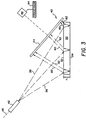
- FIG. 3 Another interferometer 40 is depicted in FIG. 3.
- Optical components of this interferometer 40 which include a point source 42, a viewing screen 44, and a camera 46, are similar to those of the interferometer 10 but are arranged much differently.
- a semiconductor wafer 50 has polished front and back side surfaces 52 and 54; but in contrast to the wafer 20, the front side surface 52 faces both the point source 42 and the viewing screen 44. Also, the wafer 50 is inclined from normal incidence to rays along an optical axis 48 of the point source 42.
- the diverging wavefront 56 is divided into two comparable wavefronts 60 and 62 by respective reflections from the front and back surfaces 52 and 54 of the wafer. Rays of the wavefront 60 reflect from the front surface 52 at respective angles of reflection equal but opposite to the angles of incidence formed by their originating rays from the diverging wavefront 56.
- Rays from the wavefront 62 refract upon entry into the wafer 50, reflect from the back surface 54, and re-refract upon exiting the wafer on paths that are parallel but laterally offset with respect to the paths of the corresponding rays of the wavefront 60.
- Both of the comparable wavefronts 60 and 62 retain substantially spherical forms, but they now appear to emanate from imaginary point sources that are relatively displaced. Since the two comparable wavefronts 60 and 62 depart from each other, a non-null interference pattern is formed on the viewing screen 44 for theoretically perfect wafers.
- the optical path length differences associated with the null condition can be calculated by a processor 64 and subtracted from the optical path length differences represented by the actual interference pattern as a measure of variations in wafer thickness "t". More exact measures of thickness variations as well as a measure of absolute thickness are obtained by modulation.
- the viewing screen 44 which functions as a diffuser, is preferably viewed by the camera 46 through light that is transmitted by the viewing screen 44.
- the camera 46 could also be positioned to view the screen 44 through light that is reflected by the screen 44.
- a fresnel lens or other focusing optic could be used in this or any of the other embodiments to collect light from the viewing screen 44 and to direct it to the camera 46.
- An interferometer 70 depicted in FIG. 4 is arranged similar to the interferometer 10 but operates in a null condition.
- a point source 72 produces a diverging spherical wavefront 86 that is reshaped into a planar wavefront 88 by a collimator 73, which can be formed by refractive, reflective, or diffractive optics.
- the planar wavefront 88 illuminates a front side surface 82 of a semiconductor wafer at normal incidence.
- the point source 72 and the collimator 73, as well as a viewing screen 74 and a camera 76, are all preferably aligned with a common optical axis 78.
- the planar wavefront 88 could also be oriented to impinge upon the front side surface 82 at a non-normal angle of incidence while preserving a null condition.
- the planar wavefront 88 is divided into two comparable wavefronts 90 and 92.
- the wavefront 90 transmits directly through the second side surface 84 to the viewing screen 74.
- the wavefront 92 reflects first from a back side surface 84 and then again from the front side surface 82 before emanating from the back side surface 84 along substantially the same path as the wavefront 90 to the viewing screen 74. Assuming that the surfaces 82 and 84 are substantially flat, the optical path length difference between the two comparable wavefronts 90 and 92 is equal to twice the thickness of the wafer 80 times the refractive index of the semiconductor material of the wafer 80.
- a processor 94 can be used to perform a conventional evaluation of the fringes appearing on the viewing screen 74 and recorded by the camera 76. Since the interfering wavefronts 90 and 92 remain substantially collimated, it would also be possible to arrange the camera 76 to view an interference pattern on the back side surface 84 of the wafer.
- FIGS. 1 and 4 The simplified interferometers of FIGS. 1 and 4 are made possible by my discovery that semiconductor wafers are both sufficiently reflective and sufficiently transmissive in the infrared spectrum to permit an interferometric comparison between a first portion of an infrared beam that is transmitted through a semiconductor wafer and a remaining portion of the infrared beam that is reflected from opposite sides of the wafer.
- C 2 I 1 • I 2 I 1 + I 2 x 100 where "I 1 " is the intensity of one of the beam portions reaching the viewing screen and "I 2 " is the intensity of the other beam portion reaching the viewing screen.
- I 1 is the intensity of one of the beam portions reaching the viewing screen
- I 2 is the intensity of the other beam portion reaching the viewing screen.
- a contrast of approximately forty percent is possible with semiconductor wafers measured in accordance with my invention.
- transmissive optical materials including optical glass do not have an index of refraction that is sufficiently different from air to maintain a beam intensity through two reflections large enough to achieve the required contrast with a portion of the same original beam that is merely transmitted.
- semiconductor materials are not transmissive. However, beginning at wavelengths near 1 ⁇ m in the infrared spectrum, semiconductor materials such as silicon become transmissive and exhibit a sufficient index of refraction to provide the required reflectivity. The precise wavelength of infrared light can be chosen to vary the sensitivity of the measurement.
- the point source 102 is similar to the point sources of the preceding embodiments, emitting a diverging beam of light 108 having a wavelength within a range at which the semiconductor wafer 106 is at least partially transmissive.
- the point source 104 emits a diverging beam 110 having a wavelength at which the semiconductor wafer 106 is substantially opaque.
- the first point source 102 can be a diode laser operating at a wavelength of 1550 nanometers
- the second point source 104 can be a HeNe laser operating at 633 nanometers.
- Collimators 112 and 114 convert the diverging beams 108 and 110 into collimated beams 116 and 118, which respectively transmit through half-wave retardation plates 120 and 122 to polarizing beamsplitters 124 and 126.
- the half-wave retardation plate 120 is adjusted with respect to the beamsplitter 124 so that substantially all of the collimated beam 116 is reflected by the beamsplitter 124 on route through a quarter-wave retardation plate 128 to a dichroic beamsplitter 130.
- the half-wave retardation plate 122 is adjusted with respect to the beamsplitter 126 to divide the collimated beam 118 into a reference beam 132 that is transmitted and a test beam 134 that is reflected.
- the reference beam 132 transmits through a quarter-wave retardation plate 136 to a reference mirror 138.
- the test beam 134 transmits through a quarter-wave retardation plate 140 to the dichroic beamsplitter 130.
- the dichroic beamsplitter 130 is wavelength sensitive for reflecting the collimated beam 116 and transmitting the collimated test beam 134.
- Both collimated beams 116 and 134 are similarly expanded by a focusing optic 142 and a collimator 144.
- the focusing optic 142 and the collimator 144 form a beam expander, which can be made either achromatic or spherochromatic with a focusing adjustment to accommodate the wavelength differences between the collimated beams 116 and 134.
- the expanded beam 116 has a wavelength that is partially transmitted and partially reflected by the semiconductor wafer 106
- the expanded test beam 134 has a wavelength that is substantially reflected by the semiconductor wafer 106.
- One portion 148 of the expanded beam 116 reflects from a front surface 150 of the wafer 106, and another portion 152 transmits through the wafer 106 and reflects from a back surface 154 of the wafer 106.
- the two beam portions 148 and 152 which have path length differences that are a function of the wafer thickness, interfere on the front surface 150 of the wafer 106 and return to the dichroic beamsplitter 130 as a first interfering beam 156.
- the quarter-wave retardation plate 128 is adjusted so the first interfering beam 156 is substantially transmitted through the beamsplitter 124.
- a focusing optic 158 forms an image of the interference pattern carried by the first interfering beam 156 on a recording surface of an infrared camera 160, and a processor 162 evaluates fringes of the interference pattern to measure thickness variations between the front and back surfaces 150 and 154 of the wafer 106.
- the expanded test beam 134 reflects from the front surface 150 of the wafer and returns to the dichroic beamsplitter 130 as a modified test beam 164 incorporating path length variations caused by irregularities in the front surface 150.
- the modified test beam 164 interferes with the reflected reference beam 132 at the beamsplitter 126 forming a second interfering beam 166 that records the path length variations undergone by the test beam 134 at the front surface 150 of the wafer 106.
- the two quarter-wave retardation plates 136 and 140 are adjusted to improve reflection and transmission efficiencies of the beamsplitter 126 for combining the reflected reference beam 132 and the modified test beam 164.
- the plates 136 and 140 also prevent light from returning to the point source 104.
- a polarizing plate 168 is adjusted to enhance contrast between the reference beam 132 and modified test beam 164 components of the second interfering beam 166.
- a focusing optic 170 forms an image of the interference pattern carried by the second interfering beam 166 on a recording surface of a CCD camera 172.
- a processor 174 which can be the same processor as the processor 162, evaluates fringes of the interference pattern to measure flatness of the wafer's front surface 150.
- a single camera sensitive to both wavelengths of the returning beams could also be used.
- the flatness of the back surface 154 can be calculated by relating both measures within a common frame of reference.
- Other configurations could also be used for simultaneously measuring flatness and thickness variations, including combinations in which flatness continues to be measured in a null condition and thickness variations are measured in a non-null condition as depicted in one of the first two embodiments.
Landscapes
- Physics & Mathematics (AREA)
- General Physics & Mathematics (AREA)
- Length Measuring Devices By Optical Means (AREA)
- Instruments For Measurement Of Length By Optical Means (AREA)
Abstract
Description
- The invention relates to the field of optical metrology and particularly to the use of interferometry for measuring thickness variations of semiconductor wafers.
- Interferometry is used in the testing of semiconductor wafers to provide measures of flatness and thickness variations. Generally, the opposite side surfaces of the wafers are both measured for flatness, and the two flatness measures are compared to determine variations in thickness. Of the two, the measurement of thickness variations is of most importance because the semiconductor wafers, which have a very high aspect ratio of diameter to thickness, tend to conform to their mounts.
- Semiconductor materials, such as silicon and gallium arsenide, are generally not transmissive within the visible spectrum.
However, the opposite side surfaces of some semiconductor wafers are highly polished so that both side surfaces can be measured by reflecting a test beam from each surface and by combining the reflected test beam with a reference beam to produce an interference pattern representative of surface variations. - One available technique using a single interferometer measures one side surface at a time. Between measures, the semiconductor wafer is remounted. Each mounting can cause distortions in the shape of the semiconductor wafer, which reduces accuracy of both flatness measurements as well as the calculated thickness variations. The remounting is also time consuming.
- Another available technique measures both side surfaces simultaneously using two interferometers. Although mounting distortions can still affect the flatness measurements, the relative measure of thickness variations is largely independent of the mounting. However, the positions of the two interferometers must be exactly known with respect to the mounting. Also, the two interferometers are expensive and difficult to maintain in the exactly known positions.
- U.S. Patent 4,653,922 to Järisch et al. discloses an interferometer that includes an arrangement of reflective optics for traversing both side surface of "non-transparent" wafers with a single test beam. Any variation in the optical path length of the test beam with respect to a reference beam is interpreted as a variation in thickness. One embodiment combines two flat mirrors with a diffraction grating for guiding the test beam, and another embodiment substitutes a folding mirror for the grating. All of these reflective optics are quite large and cumbersome to position in required alignment.
- These and other problems with known interferometric techniques for measuring semiconductor wafers are made worse by the increasing size of these wafers, which now measure as much as 30cm in diameter. One embodiment of Järish et al's interferometer requires mirrors two to three times the wafer diameter, which is impractical for such large wafers.
- US4221486 discloses a method for interferometric measurement in which light is directed onto front and rear surfaces of an object and is reflected from the front and rear surfaces to pass through a lens and onto a concave mirror. The light is reflected from the concave mirror to pass through the lens again and strikes the object at a different angle and is then reflected again by the front and rear faces of the object towards a second mirror which deflects the light onto a screen to form an interference pattern. All of the light used to form the interference pattern has been reflected from either the front or rear face of the object which is being measured.
- Polished semiconductor wafers exhibit unique qualities of reflectivity and transmissivity within the infrared spectrum, and I have discovered that these qualities enable the opposite side surface of the wafers to be compared by new interferometric configurations. In fact, it is possible to compare the two surfaces with interferometric techniques that would not be possible with similar plane-parallel objects made of optical glass.
- My invention in one or more of its embodiments exploits this discovery by simplifying interferometric apparatus for measuring thickness variations in semiconductor wafers and by extending the practicality of interferometric thickness measurement to larger size wafers. Improvements in accuracy and efficiency are also possible by comparing both side surfaces simultaneously without requiring additional optics to convey a test beam between the two side surfaces.
Accordingly, a first aspect of the present invention provides an interferometric method of measuring thickness variations of parallel-surface test pieces in a non-null condition comprising the steps of: - illuminating a first of two nominally parallel surfaces of a test piece with a non-collimated beam that strikes the first parallel surface at varying angles of incidence and emanates from a light source located adjacent to the first parallel surface of the test piece and remote form a second of the parallel surfaces of the test piece ;
- using a combination of transmission through the
first parallel surface and reflections from
both parallel surfaces to divide the non-collimated
beam into two relatively modified
beams by virtue of:
- reflecting one of the modified beams from both parallel surfaces of the test piece; and transmitting both of the relatively modified beams through both parallel surfaces of the test piece so that both beams emerge from the second parallel surface of the test piece remote from the light source ;
- forming an interference pattern between the two relatively modif ied beams that are transmitted through the test piece including the one modified beam that reflects from both parallel surfaces of the test piece;
- locating viewing optics adjacent to the second parallel surface of the test piece and remote from the light source for viewing the interference pattern; and
- evaluating the interference pattern to distinguish path length variations between the two relatively modified beams attributable to thickness variations from path length variations between the two relatively modified beams attributable to variations in the angles of incidence through which the first parallel surface of the test piece is illuminated.
-
- A second aspect of the present invention provides an interferometer for measuring thickness variations of parallel-surface test pieces comprising:
- a light source that produces a diverging beam of light for illuminating a first of two nominally parallel surfaces of a test piece with the diverging beam at varying angles of incidence;
- said light source being located adjacent to the first parallel surface of the test piece and remote from a second of the parallel surfaces of the test piece;
- a viewing screen that images an interference pattern formed between first and second portions of the diverging beam that transmit through both of the parallel surfaces of the test piece, the first beam portion being relatively modified with respect to the second beam portion by reflections from both of the parallel surfaces of the test piece;
- a processor for evaluating the interference pattern to distinguish path length variations between the two relatively modified beam portions attributable to thickness variations from path length variations between the two relatively modified beam portions attributable to the varying angles of incidence at which the first surface of the test piece is illuminated;
- said test piece being aligned along a common optical axis between said light source and said viewing screen; and
- said viewing screen being located adjacent to the second parallel surface of the test piece and remote from said light source.
-
- Thus, an interferometer, operating within a spectrum at which the semiconductor materials are at least partially transmissive (e.g. wavelengths greater than one micron, i.e. one micrometre), can be used to compare the opposite side surfaces of the semi conductor wafers in a non-null condition.
Recombining the two relatively modified beams produces an interference pattern that can be evaluated to distinguish differences between the optical path lengths of the relatively modified beams as a function of distances between the opposite side surfaces. - In the non-null condition, the optical components of the interferometer may be limited to only a point source of coherent illumination and a viewing system. A coherent light beam diverging from the point source illuminates the semiconductor wafer.
- Preferably, the viewing system includes a viewing screen and a camera sensitive to infrared radiation focused on the viewing screen. The two beam portions illuminate the viewing screen with an interference pattern formed by differences between their optical path lengths. Some of the optical path differences between the two beam portions are a result of thickness variations in the wafer, but other of these differences are attributable to variations in the angles of incidence at which the wafers are illuminated. These latter differences can be calculated in advance and used as a frame of reference (i.e. a known non-null condition) against which the further differences due to thickness variations can be compared.
- Fringes recorded by a camera for the non-null condition of measurement are preferably further evaluated by modulation to obtain more accurate measures of thickness variations or flatness in the wafers. For example, either the wavelength or the relative position of the point source can be varied in a controlled manner to modulate the fringes. The modulation allows the calculation of thickness or flatness differences between adjacent points on the wafers, and the rate of fringe modulation can be used to calculate the absolute thickness.
-
- FIG. 1 is a diagram showing a first embodiment of an interferometer in which a semiconductor wafer is viewed by transmission in a non-null condition.
- FIG. 2 is a graph showing optical path length differences caused by illuminating the semiconductor wafer with varying angles of incidence.
- FIG. 3 is a diagram showing a second embodiment of an interferometer in which the semiconductor wafer is viewed by reflection in a non-null condition.
- FIG. 4 is a diagram showing a third embodiment of an interferometer in which the semiconductor wafer is viewed by transmission in a null condition.
- FIG. 5 is a diagram showing a fourth embodiment of an interferometer in which two different wavelengths are used for measuring both thickness variations and flatness in a null condition.
-
- An
interferometer 10 depicted in FIG. 1 includes apoint source 12 of coherent infrared illumination, atransmissive viewing screen 14, and acamera 16 all aligned with a common optical axis 18. Asemiconductor wafer 20 under test includes afront surface 22 facing thepoint source 12 and a back surface 24 facing theviewing screen 14. Preferably, thewafer 20 is made from silicon or gallium arsenide, and the front andback side surfaces 22 and 24 are finely polished to at least approximate flatness and parallelism. Conventional mounting arrangements (not shown) can be used to support thesemiconductor wafer 20 in theinterferometer 10. - The
point source 12 can be the output of a single-mode optical fiber, a tightly focused and spatially filtered laser beam, or the direct output of a laser diode. A nominallyspherical wavefront 26 diverges from thepoint source 12 and impinges on thefront surface 22 at angles of incidence that progressively increase with radial distance from the optical axis 18. - Although refracted upon entry, a portion of the diverging
wavefront 26 is transmitted through thesemiconductor wafer 20 to the back surface 24 where it is divided into twocomparable wavefronts wavefront 30 refract from the back side surface 24 onto paths that are substantially parallel but laterally offset from the paths of their originating rays from the divergingwavefront 26. The amount of offset varies with the incident angles of the originating rays. Rays of thewavefront 32 reflect first from the back surface 24 and then from thefront surface 22 before finally refracting from the back surface 24 along paths that are also substantially parallel but laterally offset in an opposite direction with respect to their originating rays from the divergingwavefront 26. - The two
wavefronts wavefronts viewing screen 14 and is recorded by thecamera 16 that is sensitive to infrared light. However, in contrast to conventional interferometric practice in which a theoretically perfect test piece produces a null interference pattern, the interference pattern produced by even aperfect semiconductor wafer 20 contains a fringe pattern representing optical path length differences associated with the varying angles of incidence at which thesemiconductor wafer 20 is illuminated. This non-null condition contains a fringe density that is of approximately the same order of magnitude as the fringe density expected from normal variations in wafer thickness "t" and cannot be removed by adjusting the relative position or orientation of thesemiconductor wafer 20. - Nevertheless, the optical path length differences that produce the non-null interference pattern can be easily calculated by a
processor 34 for each point in the recorded interference pattern and subtracted from the path length differences represented by the actual interference pattern illuminating theviewing screen 14. What remain are optical path length differences caused by differences between a theoretically perfect wafer and theactual semiconductor wafer 20. Although wafer deformations and material inhomogeneities can enter into these differences, the largest remaining differences are attributable to variations in wafer thickness "t". - An example of the systematic errors attributable to the non-null condition are graphed in FIG. 2. The
semiconductor wafer 20 is assumed to have a nominal thickness of 0.75 mm and a diameter of 300 mm. Thepoint source 12 emits light having a wavelength of 1.523 µm through a numerical aperture of 0.1, and theviewing screen 14 is positioned with a 1.0 mm separation from thewafer 20. As expected, the absolute value of the optical path length difference associated with the non-null condition increases with radial distance on theviewing screen 14 from the optical axis 18. - The fringe analysis also includes conventional modulation to more accurately determine local variations in thickness. For example, either the emitted wavelength or the relative position of the point source can be varied to modulate the fringes. The rate of fringe modulation can be used to determine the absolute thickness of the
wafer 20. This rate is a known function of several variables including absolute thickness, refractive index, angle of incidence, and wavelength and can be solved for absolute thickness as the only unknown. - Another
interferometer 40 is depicted in FIG. 3. Optical components of thisinterferometer 40, which include apoint source 42, aviewing screen 44, and acamera 46, are similar to those of theinterferometer 10 but are arranged much differently. Asemiconductor wafer 50 has polished front and back side surfaces 52 and 54; but in contrast to thewafer 20, the front side surface 52 faces both thepoint source 42 and theviewing screen 44. Also, thewafer 50 is inclined from normal incidence to rays along anoptical axis 48 of thepoint source 42. - A diverging nominally
spherical wavefront 56 emitted by thepoint source 42 impinges on the front surface 52 of thewafer 50 at angles of incidence that progressively vary along a diameter of thewafer 50. The divergingwavefront 56 is divided into twocomparable wavefronts wavefront 60 reflect from the front surface 52 at respective angles of reflection equal but opposite to the angles of incidence formed by their originating rays from the divergingwavefront 56. Rays from thewavefront 62 refract upon entry into thewafer 50, reflect from theback surface 54, and re-refract upon exiting the wafer on paths that are parallel but laterally offset with respect to the paths of the corresponding rays of thewavefront 60. - Both of the
comparable wavefronts comparable wavefronts viewing screen 44 for theoretically perfect wafers. - Similar to the preceding embodiment, the optical path length differences associated with the null condition can be calculated by a
processor 64 and subtracted from the optical path length differences represented by the actual interference pattern as a measure of variations in wafer thickness "t". More exact measures of thickness variations as well as a measure of absolute thickness are obtained by modulation. - The
viewing screen 44, which functions as a diffuser, is preferably viewed by thecamera 46 through light that is transmitted by theviewing screen 44. However, thecamera 46 could also be positioned to view thescreen 44 through light that is reflected by thescreen 44. In addition, a fresnel lens or other focusing optic could be used in this or any of the other embodiments to collect light from theviewing screen 44 and to direct it to thecamera 46. - An
interferometer 70 depicted in FIG. 4 is arranged similar to theinterferometer 10 but operates in a null condition. Apoint source 72 produces a diverging spherical wavefront 86 that is reshaped into aplanar wavefront 88 by acollimator 73, which can be formed by refractive, reflective, or diffractive optics. Theplanar wavefront 88 illuminates afront side surface 82 of a semiconductor wafer at normal incidence. Thepoint source 72 and thecollimator 73, as well as a viewing screen 74 and acamera 76, are all preferably aligned with a commonoptical axis 78. However, theplanar wavefront 88 could also be oriented to impinge upon thefront side surface 82 at a non-normal angle of incidence while preserving a null condition. - At a
back side surface 84 of thewafer 80, theplanar wavefront 88 is divided into two comparable wavefronts 90 and 92. The wavefront 90 transmits directly through thesecond side surface 84 to the viewing screen 74. The wavefront 92 reflects first from aback side surface 84 and then again from thefront side surface 82 before emanating from theback side surface 84 along substantially the same path as the wavefront 90 to the viewing screen 74. Assuming that thesurfaces wafer 80 times the refractive index of the semiconductor material of thewafer 80. - Thus, absent any variation in thickness "t", a null interference pattern would be expected to illuminate the viewing screen 74. A
processor 94 can be used to perform a conventional evaluation of the fringes appearing on the viewing screen 74 and recorded by thecamera 76. Since the interfering wavefronts 90 and 92 remain substantially collimated, it would also be possible to arrange thecamera 76 to view an interference pattern on theback side surface 84 of the wafer. - The simplified interferometers of FIGS. 1 and 4 are made possible by my discovery that semiconductor wafers are both sufficiently reflective and sufficiently transmissive in the infrared spectrum to permit an interferometric comparison between a first portion of an infrared beam that is transmitted through a semiconductor wafer and a remaining portion of the infrared beam that is reflected from opposite sides of the wafer.
- A sufficient contrast "C" between the two beam portions is needed to produce useful fringe patterns. Generally, this contrast should be ten percent or more as calculated by the following equation:
- Most transmissive optical materials including optical glass do not have an index of refraction that is sufficiently different from air to maintain a beam intensity through two reflections large enough to achieve the required contrast with a portion of the same original beam that is merely transmitted. Within the visible spectrum, semiconductor materials are not transmissive. However, beginning at wavelengths near 1 µm in the infrared spectrum, semiconductor materials such as silicon become transmissive and exhibit a sufficient index of refraction to provide the required reflectivity. The precise wavelength of infrared light can be chosen to vary the sensitivity of the measurement.
- An
interferometer 100 depicted in FIG. 5, which is also arranged to operate in a null condition, includes twodifferent point sources semiconductor wafer 106. Thepoint source 102 is similar to the point sources of the preceding embodiments, emitting a diverging beam oflight 108 having a wavelength within a range at which thesemiconductor wafer 106 is at least partially transmissive. Thepoint source 104 emits a divergingbeam 110 having a wavelength at which thesemiconductor wafer 106 is substantially opaque. For example, thefirst point source 102 can be a diode laser operating at a wavelength of 1550 nanometers, and thesecond point source 104 can be a HeNe laser operating at 633 nanometers. -
Collimators beams beams wave retardation plates polarizing beamsplitters wave retardation plate 120 is adjusted with respect to thebeamsplitter 124 so that substantially all of the collimatedbeam 116 is reflected by thebeamsplitter 124 on route through a quarter-wave retardation plate 128 to adichroic beamsplitter 130. - The half-
wave retardation plate 122 is adjusted with respect to thebeamsplitter 126 to divide the collimatedbeam 118 into areference beam 132 that is transmitted and a test beam 134 that is reflected. Thereference beam 132 transmits through a quarter-wave retardation plate 136 to areference mirror 138. The test beam 134 transmits through a quarter-wave retardation plate 140 to thedichroic beamsplitter 130. - The
dichroic beamsplitter 130 is wavelength sensitive for reflecting the collimatedbeam 116 and transmitting the collimated test beam 134. Both collimatedbeams 116 and 134 are similarly expanded by a focusingoptic 142 and acollimator 144. Together, the focusingoptic 142 and thecollimator 144 form a beam expander, which can be made either achromatic or spherochromatic with a focusing adjustment to accommodate the wavelength differences between thecollimated beams 116 and 134. The expandedbeam 116 has a wavelength that is partially transmitted and partially reflected by thesemiconductor wafer 106, and the expanded test beam 134 has a wavelength that is substantially reflected by thesemiconductor wafer 106. - One
portion 148 of the expandedbeam 116 reflects from afront surface 150 of thewafer 106, and anotherportion 152 transmits through thewafer 106 and reflects from aback surface 154 of thewafer 106. The twobeam portions front surface 150 of thewafer 106 and return to thedichroic beamsplitter 130 as a first interferingbeam 156. - The quarter-
wave retardation plate 128 is adjusted so the first interferingbeam 156 is substantially transmitted through thebeamsplitter 124. A focusingoptic 158 forms an image of the interference pattern carried by the first interferingbeam 156 on a recording surface of aninfrared camera 160, and aprocessor 162 evaluates fringes of the interference pattern to measure thickness variations between the front andback surfaces wafer 106. - The expanded test beam 134 reflects from the
front surface 150 of the wafer and returns to thedichroic beamsplitter 130 as a modifiedtest beam 164 incorporating path length variations caused by irregularities in thefront surface 150. The modifiedtest beam 164 interferes with the reflectedreference beam 132 at thebeamsplitter 126 forming a second interferingbeam 166 that records the path length variations undergone by the test beam 134 at thefront surface 150 of thewafer 106. - The two quarter-
wave retardation plates 136 and 140 are adjusted to improve reflection and transmission efficiencies of thebeamsplitter 126 for combining the reflectedreference beam 132 and the modifiedtest beam 164. Theplates 136 and 140 also prevent light from returning to thepoint source 104. Apolarizing plate 168 is adjusted to enhance contrast between thereference beam 132 and modifiedtest beam 164 components of the second interferingbeam 166. - A focusing
optic 170 forms an image of the interference pattern carried by the second interferingbeam 166 on a recording surface of aCCD camera 172. Aprocessor 174, which can be the same processor as theprocessor 162, evaluates fringes of the interference pattern to measure flatness of the wafer'sfront surface 150. A single camera sensitive to both wavelengths of the returning beams could also be used. - Once both the flatness of
front surface 150 and the thickness variations between the front andback surfaces back surface 154 can be calculated by relating both measures within a common frame of reference. Other configurations could also be used for simultaneously measuring flatness and thickness variations, including combinations in which flatness continues to be measured in a null condition and thickness variations are measured in a non-null condition as depicted in one of the first two embodiments. - Although the invention is specifically designed to work with semiconductor wafers, other nominally parallel surface test pieces made from materials meeting the recited criteria for transmissivity and reflectivity could also be measured in accordance with my invention. Variables such as incident angles and point source divergence can be optimized to suite particular applications. Also, the interferometric measurement of test surfaces under non-null conditions may be applicable to a wider range of materials, test surfaces, and types of measures.
Claims (10)
- An interferometric method of measuring thickness variations of parallel-surface test pieces in a non-null condition comprising the steps of:illuminating a first of two nominally parallel surfaces (22, 24) of a test piece (20) with a non-collimated beam (26) that strikes the first parallel surface (22) at varying angles of incidence and emanates from a light source (12) located adjacent to the first parallel surface (22) of the test piece (20) and remote form a second of the parallel surfaces (24) of the test piece (20);using a combination of transmission through the first parallel surface (22) and reflections from both parallel surfaces (22,24) to divide the non-collimated beam (26) into two relatively modified beams (30,32) by virtue of:reflecting one of the modified beams (32) from both parallel surfaces (22,24) of the test piece; andtransmitting both of the relatively modified beams (30,32) through both parallel surfaces (22,24) of the test piece (20) so that both beams (30,32) emerge from the second parallel surface (24) of the test piece (20) remote from the light source (12);forming an interference pattern between the two relatively modified beams (30,32) that are transmitted through the test piece (20) including the one modified beam (32) that reflects from both parallel surfaces (22,24) of the test piece;locating viewing optics(14) adjacent to the second parallel surface (24) of the test piece (20) and remote from the light source (12) for viewing the interference pattern; andevaluating the interference pattern to distinguish path length variations between the two relatively modified beams (30,32) attributable to thickness variations from path length variations between the two relatively modified beams (30,32) attributable to variations in the angles of incidence through which the first parallel surface (22) of the test piece (20) is illuminated.
- The method of claim 1 in which said step of illuminating includes illuminating the first parallel surface (22) of the test piece(20) with a diverging beam (26) .
- The method of claim 2 in which said step of using divides the diverging beam (26) into two further diverging beams (30,32).
- The method of claim 1 in which said step of locating includes locating a viewing screen (14) adjacent to the second (24) of the parallel surfaces of the test piece (20) and remote from the light source (12).
- The method of claim 4 in which said step of locating includes aligning the light source (12), the test piece (20) and the viewing screen (14) along a common optical axis (18).
- The method of claim 1 in which the test piece (20) is a semiconductor wafer that is substantially opaque at wavelengths less than one micrometre.
- The method of claim 6 in which the beam (26) emanating from the light source (12) has a wavelength greater than one micrometre.
- An interferometer (10) for measuring thickness variations of parallel-surface test pieces (20) comprising:a light source (12) that produces a diverging beam of light (26) for illuminating a first of two nominally parallel surfaces (22,24) of a test piece (20) with the diverging beam (26) at varying angles of incidence;said light source (12) being located adjacent to the first parallel surface (22) of the test piece (20) and remote from a second (24) of the parallel surfaces of the test piece (20);a viewing screen (14) that images an interference pattern formed between first (32) and second (30) portions of the diverging beam (26) that transmit through both of the parallel surfaces (22,24) of the test piece (20) , the first beam portion (32) being relatively modified with respect to the second beam portion (30) by reflections from both of the parallel surfaces (22, 24) of the test piece (20);a processor (34) for evaluating the interference pattern to distinguish path length variations between the two relatively modified beam portions (30,32) attributable to thickness variations from path length variations between the two relatively modified beam portions (30,32) attributable to the varying angles of incidence at which the first surface of the test piece (20) is illuminated;said test piece (20) being aligned along a common optical axis (18) between said light source (12) and said viewing screen (14); andsaid viewing screen (14) being located adjacent to the second parallel surface (24) of the test piece (20) and remote from said light source (12).
- The interferometer of claim 8 in which said light source (12) produces a diverging beam of light (26) having a wavelength greater than one micrometre.
- The interferometer of claim 8 in which the test piece (20) is located closer to said viewing screen (14) than said light source (12).
Applications Claiming Priority (3)
| Application Number | Priority Date | Filing Date | Title |
|---|---|---|---|
| US1876996P | 1996-05-31 | 1996-05-31 | |
| US18769P | 1996-05-31 | ||
| PCT/US1997/009081 WO1997045698A1 (en) | 1996-05-31 | 1997-05-30 | Interferometer for measuring thickness variations of semiconductor wafers |
Publications (2)
| Publication Number | Publication Date |
|---|---|
| EP0902874A1 EP0902874A1 (en) | 1999-03-24 |
| EP0902874B1 true EP0902874B1 (en) | 2004-01-28 |
Family
ID=21789697
Family Applications (1)
| Application Number | Title | Priority Date | Filing Date |
|---|---|---|---|
| EP97927809A Expired - Lifetime EP0902874B1 (en) | 1996-05-31 | 1997-05-30 | Interferometer for measuring thickness variations of semiconductor wafers |
Country Status (7)
| Country | Link |
|---|---|
| US (1) | US5909282A (en) |
| EP (1) | EP0902874B1 (en) |
| JP (1) | JP3392145B2 (en) |
| KR (1) | KR20000016177A (en) |
| AT (1) | ATE258675T1 (en) |
| DE (1) | DE69727376D1 (en) |
| WO (1) | WO1997045698A1 (en) |
Families Citing this family (22)
| Publication number | Priority date | Publication date | Assignee | Title |
|---|---|---|---|---|
| US6381356B1 (en) * | 1996-10-23 | 2002-04-30 | Nec Corporation | Method and apparatus for inspecting high-precision patterns |
| US6366688B1 (en) * | 1998-06-13 | 2002-04-02 | Samsung Electronics Co., Ltd. | Apparatus and method for contact failure inspection in semiconductor devices |
| US6418604B1 (en) * | 1998-07-31 | 2002-07-16 | Imation Corp. | Method of fabricating die coater parts |
| US6368881B1 (en) * | 2000-02-29 | 2002-04-09 | International Business Machines Corporation | Wafer thickness control during backside grind |
| WO2002011183A2 (en) * | 2000-07-31 | 2002-02-07 | Ade Corporation | Shape accuracy improvement using a novel calibration approach |
| DE10130902A1 (en) * | 2001-06-27 | 2003-01-16 | Zeiss Carl | Interferometer system, method for recording an interferogram and method for providing and producing an object with a target surface |
| US6690690B2 (en) | 2002-05-29 | 2004-02-10 | Lightgage, Inc. | Tunable laser system having an adjustable external cavity |
| US7130059B2 (en) * | 2002-06-24 | 2006-10-31 | Light Gage, Inc | Common-path frequency-scanning interferometer |
| WO2004001330A2 (en) * | 2002-06-24 | 2003-12-31 | Lightgage, Inc. | Multi-stage data processing for frequency-scanning interferometer |
| AU2003247725A1 (en) | 2002-07-01 | 2004-01-19 | Lightgage, Inc. | Interferometer system of compact configuration |
| US7057742B2 (en) * | 2002-07-01 | 2006-06-06 | Lightgage, Inc. | Frequency-scanning interferometer with non-specular reference surface |
| JP3742801B2 (en) * | 2003-03-18 | 2006-02-08 | 独立行政法人科学技術振興機構 | Film thickness acquisition method |
| US6847458B2 (en) * | 2003-03-20 | 2005-01-25 | Phase Shift Technology, Inc. | Method and apparatus for measuring the shape and thickness variation of polished opaque plates |
| US20050168753A1 (en) * | 2004-02-03 | 2005-08-04 | Infineon Technologies North America Corp. | Optical measurement of device features using interferometric illumination |
| WO2007044786A2 (en) * | 2005-10-11 | 2007-04-19 | Zygo Corporation | Interferometry method and system including spectral decomposition |
| KR100933313B1 (en) * | 2007-11-06 | 2009-12-22 | 한국표준과학연구원 | Wafer thickness change measuring method and apparatus |
| KR100988454B1 (en) * | 2008-01-31 | 2010-10-18 | 에스엔유 프리시젼 주식회사 | Method for measuring thickness |
| KR100942236B1 (en) | 2008-04-08 | 2010-02-16 | 충북대학교 산학협력단 | Measurement error correcting method for the thick of glass panel |
| KR101895183B1 (en) * | 2010-11-12 | 2018-09-04 | 에베 그룹 에. 탈너 게엠베하 | Measuring device and method for measuring layer thicknesses and defects in a wafer stcak |
| US8687204B2 (en) * | 2011-03-24 | 2014-04-01 | Canon Kabushiki Kaisha | Method and apparatus for measuring refractive index based on a ratio between a number of second fringes divided by a difference of the number of second fringes minus a number of first fringes |
| US9341580B2 (en) | 2014-06-27 | 2016-05-17 | Applied Materials, Inc. | Linear inspection system |
| CN109001209A (en) * | 2018-05-29 | 2018-12-14 | 宁国中辰密封件有限公司 | A kind of injecting glue detection device of sealing strip |
Family Cites Families (21)
| Publication number | Priority date | Publication date | Assignee | Title |
|---|---|---|---|---|
| US2518647A (en) * | 1948-01-07 | 1950-08-15 | Celanese Corp | Interferometer means for thickness measurements |
| US3735036A (en) * | 1970-10-26 | 1973-05-22 | Express I M Co | Real time interferometry contour mapping system |
| DE2758149C2 (en) * | 1977-12-27 | 1979-10-04 | Ibm Deutschland Gmbh, 7000 Stuttgart | Interferometric method with λ / 4 resolution for distance, thickness and / or flatness measurement |
| JPS5535214A (en) * | 1978-09-04 | 1980-03-12 | Asahi Chem Ind Co Ltd | Method and device for film-thickness measurement making use of infrared-ray interference |
| DE3048558A1 (en) * | 1980-12-22 | 1982-07-22 | Battelle-Institut E.V., 6000 Frankfurt | Contactless measurement of contact lenses by topographical evaluation - using parallel and perpendicular collimated lens transmission and interferometry |
| US4606638A (en) * | 1983-11-03 | 1986-08-19 | Zygo Corporation | Distance measuring interferometer and method of use |
| DE3471368D1 (en) * | 1984-10-31 | 1988-06-23 | Ibm Deutschland | Interferometric thickness analyzer and measuring method |
| DD265055A3 (en) * | 1986-07-29 | 1989-02-22 | Technisches Glas Veb K | ARRANGEMENT FOR INTERFEROMETRIC CLEARANCE AND THICKNESS MEASUREMENT |
| JPS63222207A (en) * | 1987-03-11 | 1988-09-16 | Japan Spectroscopic Co | Apparatus for measuring depth of recessed part and thickness of film |
| SU1747877A1 (en) * | 1990-02-28 | 1992-07-15 | Северо-Западный Заочный Политехнический Институт | Interference method of measurement of the semiconductor layer thickness |
| US5333049A (en) * | 1991-12-06 | 1994-07-26 | Hughes Aircraft Company | Apparatus and method for interferometrically measuring the thickness of thin films using full aperture irradiation |
| US5386119A (en) * | 1993-03-25 | 1995-01-31 | Hughes Aircraft Company | Apparatus and method for thick wafer measurement |
| JP3234353B2 (en) * | 1993-06-15 | 2001-12-04 | 富士写真フイルム株式会社 | Tomographic information reader |
| JPH074922A (en) * | 1993-06-21 | 1995-01-10 | Jasco Corp | Apparatus and method for measurement of film thickness of semiconductor multilayer thin film |
| US5555472A (en) * | 1993-12-22 | 1996-09-10 | Integrated Process Equipment Corp. | Method and apparatus for measuring film thickness in multilayer thin film stack by comparison to a reference library of theoretical signatures |
| US5471303A (en) * | 1994-04-29 | 1995-11-28 | Wyko Corporation | Combination of white-light scanning and phase-shifting interferometry for surface profile measurements |
| US5513553A (en) * | 1994-07-13 | 1996-05-07 | Gleasman; Vernon E. | Hydraulic machine with gear-mounted swash-plate |
| US5515167A (en) * | 1994-09-13 | 1996-05-07 | Hughes Aircraft Company | Transparent optical chuck incorporating optical monitoring |
| US5502564A (en) * | 1994-09-13 | 1996-03-26 | Hughes Aircraft Company | Substrate thickness measurement using oblique incidence multispectral interferometry |
| US5596409A (en) * | 1995-03-22 | 1997-01-21 | Eastman Kodak Company | Associated dual interferometric measurement method for determining a physical property of an object |
| US5555471A (en) * | 1995-05-24 | 1996-09-10 | Wyko Corporation | Method for measuring thin-film thickness and step height on the surface of thin-film/substrate test samples by phase-shifting interferometry |
-
1997
- 1997-05-30 WO PCT/US1997/009081 patent/WO1997045698A1/en active IP Right Grant
- 1997-05-30 JP JP54291297A patent/JP3392145B2/en not_active Expired - Fee Related
- 1997-05-30 EP EP97927809A patent/EP0902874B1/en not_active Expired - Lifetime
- 1997-05-30 KR KR1019980709745A patent/KR20000016177A/en not_active Application Discontinuation
- 1997-05-30 US US08/866,540 patent/US5909282A/en not_active Expired - Fee Related
- 1997-05-30 AT AT97927809T patent/ATE258675T1/en not_active IP Right Cessation
- 1997-05-30 DE DE69727376T patent/DE69727376D1/en not_active Expired - Lifetime
Also Published As
| Publication number | Publication date |
|---|---|
| EP0902874A1 (en) | 1999-03-24 |
| JP2000501508A (en) | 2000-02-08 |
| DE69727376D1 (en) | 2004-03-04 |
| ATE258675T1 (en) | 2004-02-15 |
| WO1997045698A1 (en) | 1997-12-04 |
| JP3392145B2 (en) | 2003-03-31 |
| KR20000016177A (en) | 2000-03-25 |
| US5909282A (en) | 1999-06-01 |
Similar Documents
| Publication | Publication Date | Title |
|---|---|---|
| EP0902874B1 (en) | Interferometer for measuring thickness variations of semiconductor wafers | |
| US4872755A (en) | Interferometer for measuring optical phase differences | |
| US6249351B1 (en) | Grazing incidence interferometer and method | |
| KR101232204B1 (en) | Equal-path interferometer | |
| JP2997047B2 (en) | Optical measuring device | |
| US7466427B2 (en) | Vibration-resistant interferometer apparatus | |
| US7538890B2 (en) | Wavefront-measuring interferometer apparatus, and light beam measurement apparatus and method thereof | |
| WO2003067182A1 (en) | Shearing interference measuring method and shearing interferometer, production method of projection optical system, projection optical system, and projection exposure system | |
| US4105335A (en) | Interferometric optical phase discrimination apparatus | |
| US6590654B1 (en) | Polarized illumination and detection for metrological applications | |
| JPH08334606A (en) | Lens | |
| JPH06194125A (en) | Method and apparatus for detecting deviation of object from focal point of objective lens or change in position | |
| JPH05500853A (en) | Method and apparatus for determining glass tube wall thickness | |
| JP3461566B2 (en) | Interferometer for measuring cone shape | |
| JP3010085B2 (en) | Hologram interferometer | |
| JP2966950B2 (en) | Sample displacement measuring device | |
| JPH11325848A (en) | Aspherical surface shape measurement device | |
| GB2333834A (en) | Interferometer with deadpath error compensation | |
| JPH02259512A (en) | Integrated interference measuring instrument | |
| SU1728650A1 (en) | Interferometer for controlling concave aspheric surfaces | |
| SU1762116A1 (en) | Diffraction interferometer | |
| SU1456779A1 (en) | Method and apparatus for measuring parameters of roughness of slightly rough surface | |
| JPH0334002B2 (en) | ||
| CN114577111A (en) | Surface shape detection system and detection method | |
| JP2000088544A (en) | Method and equipment for measuring plane shape |
Legal Events
| Date | Code | Title | Description |
|---|---|---|---|
| PUAI | Public reference made under article 153(3) epc to a published international application that has entered the european phase |
Free format text: ORIGINAL CODE: 0009012 |
|
| 17P | Request for examination filed |
Effective date: 19981221 |
|
| AK | Designated contracting states |
Kind code of ref document: A1 Designated state(s): AT BE CH DE FR GB IE IT LI SE |
|
| 17Q | First examination report despatched |
Effective date: 20020729 |
|
| GRAP | Despatch of communication of intention to grant a patent |
Free format text: ORIGINAL CODE: EPIDOSNIGR1 |
|
| GRAS | Grant fee paid |
Free format text: ORIGINAL CODE: EPIDOSNIGR3 |
|
| GRAA | (expected) grant |
Free format text: ORIGINAL CODE: 0009210 |
|
| AK | Designated contracting states |
Kind code of ref document: B1 Designated state(s): AT BE CH DE FR GB IE IT LI SE |
|
| PG25 | Lapsed in a contracting state [announced via postgrant information from national office to epo] |
Ref country code: LI Free format text: LAPSE BECAUSE OF FAILURE TO SUBMIT A TRANSLATION OF THE DESCRIPTION OR TO PAY THE FEE WITHIN THE PRESCRIBED TIME-LIMIT Effective date: 20040128 Ref country code: IT Free format text: LAPSE BECAUSE OF FAILURE TO SUBMIT A TRANSLATION OF THE DESCRIPTION OR TO PAY THE FEE WITHIN THE PRESCRIBED TIME-LIMIT;WARNING: LAPSES OF ITALIAN PATENTS WITH EFFECTIVE DATE BEFORE 2007 MAY HAVE OCCURRED AT ANY TIME BEFORE 2007. THE CORRECT EFFECTIVE DATE MAY BE DIFFERENT FROM THE ONE RECORDED. Effective date: 20040128 Ref country code: FR Free format text: LAPSE BECAUSE OF FAILURE TO SUBMIT A TRANSLATION OF THE DESCRIPTION OR TO PAY THE FEE WITHIN THE PRESCRIBED TIME-LIMIT Effective date: 20040128 Ref country code: CH Free format text: LAPSE BECAUSE OF FAILURE TO SUBMIT A TRANSLATION OF THE DESCRIPTION OR TO PAY THE FEE WITHIN THE PRESCRIBED TIME-LIMIT Effective date: 20040128 Ref country code: BE Free format text: LAPSE BECAUSE OF FAILURE TO SUBMIT A TRANSLATION OF THE DESCRIPTION OR TO PAY THE FEE WITHIN THE PRESCRIBED TIME-LIMIT Effective date: 20040128 Ref country code: AT Free format text: LAPSE BECAUSE OF FAILURE TO SUBMIT A TRANSLATION OF THE DESCRIPTION OR TO PAY THE FEE WITHIN THE PRESCRIBED TIME-LIMIT Effective date: 20040128 |
|
| REG | Reference to a national code |
Ref country code: GB Ref legal event code: FG4D |
|
| REG | Reference to a national code |
Ref country code: CH Ref legal event code: EP |
|
| REG | Reference to a national code |
Ref country code: IE Ref legal event code: FG4D |
|
| REF | Corresponds to: |
Ref document number: 69727376 Country of ref document: DE Date of ref document: 20040304 Kind code of ref document: P |
|
| PG25 | Lapsed in a contracting state [announced via postgrant information from national office to epo] |
Ref country code: SE Free format text: LAPSE BECAUSE OF FAILURE TO SUBMIT A TRANSLATION OF THE DESCRIPTION OR TO PAY THE FEE WITHIN THE PRESCRIBED TIME-LIMIT Effective date: 20040428 |
|
| PG25 | Lapsed in a contracting state [announced via postgrant information from national office to epo] |
Ref country code: DE Free format text: LAPSE BECAUSE OF FAILURE TO SUBMIT A TRANSLATION OF THE DESCRIPTION OR TO PAY THE FEE WITHIN THE PRESCRIBED TIME-LIMIT Effective date: 20040429 |
|
| PG25 | Lapsed in a contracting state [announced via postgrant information from national office to epo] |
Ref country code: IE Free format text: LAPSE BECAUSE OF NON-PAYMENT OF DUE FEES Effective date: 20040531 |
|
| PGFP | Annual fee paid to national office [announced via postgrant information from national office to epo] |
Ref country code: GB Payment date: 20040623 Year of fee payment: 8 |
|
| REG | Reference to a national code |
Ref country code: CH Ref legal event code: PL |
|
| PLBE | No opposition filed within time limit |
Free format text: ORIGINAL CODE: 0009261 |
|
| STAA | Information on the status of an ep patent application or granted ep patent |
Free format text: STATUS: NO OPPOSITION FILED WITHIN TIME LIMIT |
|
| 26N | No opposition filed |
Effective date: 20041029 |
|
| EN | Fr: translation not filed | ||
| REG | Reference to a national code |
Ref country code: IE Ref legal event code: MM4A |
|
| PG25 | Lapsed in a contracting state [announced via postgrant information from national office to epo] |
Ref country code: GB Free format text: LAPSE BECAUSE OF NON-PAYMENT OF DUE FEES Effective date: 20050530 |
|
| GBPC | Gb: european patent ceased through non-payment of renewal fee |
Effective date: 20050530 |