EP0893915A2 - Compact image sensor with display integrally attached - Google Patents
Compact image sensor with display integrally attached Download PDFInfo
- Publication number
- EP0893915A2 EP0893915A2 EP98201979A EP98201979A EP0893915A2 EP 0893915 A2 EP0893915 A2 EP 0893915A2 EP 98201979 A EP98201979 A EP 98201979A EP 98201979 A EP98201979 A EP 98201979A EP 0893915 A2 EP0893915 A2 EP 0893915A2
- Authority
- EP
- European Patent Office
- Prior art keywords
- array
- display
- photosensor
- lenslet
- image
- Prior art date
- Legal status (The legal status is an assumption and is not a legal conclusion. Google has not performed a legal analysis and makes no representation as to the accuracy of the status listed.)
- Withdrawn
Links
- 238000003491 array Methods 0.000 claims abstract description 19
- 238000012545 processing Methods 0.000 claims abstract description 14
- 230000005855 radiation Effects 0.000 claims description 28
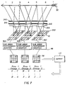
- 230000006870 function Effects 0.000 claims description 14
- 239000000463 material Substances 0.000 claims description 4
- 239000004065 semiconductor Substances 0.000 claims description 4
- 239000003086 colorant Substances 0.000 claims description 3
- 238000003860 storage Methods 0.000 claims description 3
- 239000000758 substrate Substances 0.000 abstract description 18
- 230000003287 optical effect Effects 0.000 description 16
- 229910052751 metal Inorganic materials 0.000 description 13
- 239000002184 metal Substances 0.000 description 13
- 238000000034 method Methods 0.000 description 11
- XUIMIQQOPSSXEZ-UHFFFAOYSA-N Silicon Chemical compound [Si] XUIMIQQOPSSXEZ-UHFFFAOYSA-N 0.000 description 10
- 230000002596 correlated effect Effects 0.000 description 10
- 238000005070 sampling Methods 0.000 description 10
- 229910052710 silicon Inorganic materials 0.000 description 10
- 239000010703 silicon Substances 0.000 description 10
- 239000011521 glass Substances 0.000 description 9
- 230000000875 corresponding effect Effects 0.000 description 7
- 230000008569 process Effects 0.000 description 7
- 230000000694 effects Effects 0.000 description 6
- AMGQUBHHOARCQH-UHFFFAOYSA-N indium;oxotin Chemical compound [In].[Sn]=O AMGQUBHHOARCQH-UHFFFAOYSA-N 0.000 description 6
- 239000002131 composite material Substances 0.000 description 5
- 230000009977 dual effect Effects 0.000 description 5
- 230000005496 eutectics Effects 0.000 description 4
- 238000001465 metallisation Methods 0.000 description 4
- 238000012552 review Methods 0.000 description 4
- 230000035945 sensitivity Effects 0.000 description 4
- 125000006850 spacer group Chemical group 0.000 description 4
- 238000012360 testing method Methods 0.000 description 4
- 238000012546 transfer Methods 0.000 description 4
- 239000012141 concentrate Substances 0.000 description 3
- 230000007423 decrease Effects 0.000 description 3
- 238000010586 diagram Methods 0.000 description 3
- 238000010348 incorporation Methods 0.000 description 3
- 230000010354 integration Effects 0.000 description 3
- 238000004519 manufacturing process Methods 0.000 description 3
- 229920002120 photoresistant polymer Polymers 0.000 description 3
- RTZKZFJDLAIYFH-UHFFFAOYSA-N Diethyl ether Chemical compound CCOCC RTZKZFJDLAIYFH-UHFFFAOYSA-N 0.000 description 2
- 239000004593 Epoxy Substances 0.000 description 2
- 230000004075 alteration Effects 0.000 description 2
- 230000003321 amplification Effects 0.000 description 2
- 230000003247 decreasing effect Effects 0.000 description 2
- 238000009792 diffusion process Methods 0.000 description 2
- 238000005530 etching Methods 0.000 description 2
- 238000002347 injection Methods 0.000 description 2
- 239000007924 injection Substances 0.000 description 2
- 238000001459 lithography Methods 0.000 description 2
- 239000011159 matrix material Substances 0.000 description 2
- 238000003199 nucleic acid amplification method Methods 0.000 description 2
- 239000010453 quartz Substances 0.000 description 2
- 230000009467 reduction Effects 0.000 description 2
- VYPSYNLAJGMNEJ-UHFFFAOYSA-N silicon dioxide Inorganic materials O=[Si]=O VYPSYNLAJGMNEJ-UHFFFAOYSA-N 0.000 description 2
- 229910000679 solder Inorganic materials 0.000 description 2
- 241000287181 Sturnus vulgaris Species 0.000 description 1
- 229910052782 aluminium Inorganic materials 0.000 description 1
- XAGFODPZIPBFFR-UHFFFAOYSA-N aluminium Chemical compound [Al] XAGFODPZIPBFFR-UHFFFAOYSA-N 0.000 description 1
- 238000004458 analytical method Methods 0.000 description 1
- 230000009286 beneficial effect Effects 0.000 description 1
- 239000011230 binding agent Substances 0.000 description 1
- 230000015572 biosynthetic process Effects 0.000 description 1
- 239000003990 capacitor Substances 0.000 description 1
- 239000004020 conductor Substances 0.000 description 1
- 238000012937 correction Methods 0.000 description 1
- 239000006059 cover glass Substances 0.000 description 1
- 238000013500 data storage Methods 0.000 description 1
- 238000000708 deep reactive-ion etching Methods 0.000 description 1
- 238000000151 deposition Methods 0.000 description 1
- 238000013461 design Methods 0.000 description 1
- 238000006073 displacement reaction Methods 0.000 description 1
- 238000009713 electroplating Methods 0.000 description 1
- 230000008030 elimination Effects 0.000 description 1
- 238000003379 elimination reaction Methods 0.000 description 1
- 238000005516 engineering process Methods 0.000 description 1
- PCHJSUWPFVWCPO-UHFFFAOYSA-N gold Chemical compound [Au] PCHJSUWPFVWCPO-UHFFFAOYSA-N 0.000 description 1
- 229910052737 gold Inorganic materials 0.000 description 1
- 239000010931 gold Substances 0.000 description 1
- 238000005286 illumination Methods 0.000 description 1
- 238000003384 imaging method Methods 0.000 description 1
- 238000005468 ion implantation Methods 0.000 description 1
- 238000013507 mapping Methods 0.000 description 1
- 238000012986 modification Methods 0.000 description 1
- 230000004048 modification Effects 0.000 description 1
- 239000002991 molded plastic Substances 0.000 description 1
- 230000003647 oxidation Effects 0.000 description 1
- 238000007254 oxidation reaction Methods 0.000 description 1
- 238000000059 patterning Methods 0.000 description 1
- 238000001020 plasma etching Methods 0.000 description 1
- 239000004033 plastic Substances 0.000 description 1
- 230000004044 response Effects 0.000 description 1
- 238000012216 screening Methods 0.000 description 1
- 238000000926 separation method Methods 0.000 description 1
- 238000005476 soldering Methods 0.000 description 1
- 238000004544 sputter deposition Methods 0.000 description 1
- XOLBLPGZBRYERU-UHFFFAOYSA-N tin dioxide Chemical compound O=[Sn]=O XOLBLPGZBRYERU-UHFFFAOYSA-N 0.000 description 1
- 229910001887 tin oxide Inorganic materials 0.000 description 1
- 238000007740 vapor deposition Methods 0.000 description 1
Images


Classifications
-
- H—ELECTRICITY
- H01—ELECTRIC ELEMENTS
- H01L—SEMICONDUCTOR DEVICES NOT COVERED BY CLASS H10
- H01L27/00—Devices consisting of a plurality of semiconductor or other solid-state components formed in or on a common substrate
- H01L27/14—Devices consisting of a plurality of semiconductor or other solid-state components formed in or on a common substrate including semiconductor components sensitive to infrared radiation, light, electromagnetic radiation of shorter wavelength or corpuscular radiation and specially adapted either for the conversion of the energy of such radiation into electrical energy or for the control of electrical energy by such radiation
- H01L27/144—Devices controlled by radiation
- H01L27/146—Imager structures
- H01L27/14601—Structural or functional details thereof
- H01L27/14625—Optical elements or arrangements associated with the device
- H01L27/14627—Microlenses
-
- G—PHYSICS
- G02—OPTICS
- G02B—OPTICAL ELEMENTS, SYSTEMS OR APPARATUS
- G02B3/00—Simple or compound lenses
- G02B3/0006—Arrays
- G02B3/0037—Arrays characterized by the distribution or form of lenses
- G02B3/0056—Arrays characterized by the distribution or form of lenses arranged along two different directions in a plane, e.g. honeycomb arrangement of lenses
-
- H—ELECTRICITY
- H04—ELECTRIC COMMUNICATION TECHNIQUE
- H04N—PICTORIAL COMMUNICATION, e.g. TELEVISION
- H04N25/00—Circuitry of solid-state image sensors [SSIS]; Control thereof
- H04N25/40—Extracting pixel data from image sensors by controlling scanning circuits, e.g. by modifying the number of pixels sampled or to be sampled
- H04N25/41—Extracting pixel data from a plurality of image sensors simultaneously picking up an image, e.g. for increasing the field of view by combining the outputs of a plurality of sensors
Landscapes
- Physics & Mathematics (AREA)
- Engineering & Computer Science (AREA)
- Power Engineering (AREA)
- General Physics & Mathematics (AREA)
- Microelectronics & Electronic Packaging (AREA)
- Electromagnetism (AREA)
- Condensed Matter Physics & Semiconductors (AREA)
- Computer Hardware Design (AREA)
- Optics & Photonics (AREA)
- Multimedia (AREA)
- Signal Processing (AREA)
- Devices For Indicating Variable Information By Combining Individual Elements (AREA)
- Transforming Light Signals Into Electric Signals (AREA)
- Control Of Indicators Other Than Cathode Ray Tubes (AREA)
- Cameras In General (AREA)
- Solid State Image Pick-Up Elements (AREA)
- Color Television Image Signal Generators (AREA)
Abstract
Description
n = number of transistors on the output side "To" of the current mirror, or
β = transistor current gain (typically between 50 and 200 for bipolar transistors).

- 10
- unit pixel subassembly
- 20
- photosensor
- 22
- output
- 24
- transfer gate
- 26
- reset gate
- 30
- multiplying current mirror
- 321 -32n
- transistors
- 34
- input side transistor
- 36
- transistor
- 40
- correlated double sampling circuit (CDS)
- 42
- current amplifiers
- 44
- current amplifiers
- 46
- integrating amplifier
- 48
- sub array photosensor inverter
- 50
- data bus
- 54
- pixel display driver element
- 56
- analog-to-digital converter
- 58
- memory
- 60
- row address decoder line
- 62
- column address decoder line
- 80
- multiplexing and clocking circuit
- 90
- object (arrow)
- 100
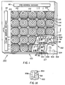
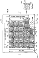
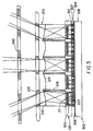
- photosensor array
- 200
- compact image capture and display device (digital camera)
- 210
- lenslet array
- 212
- lenslets
- 213
- optical axis
- 214
- mechanical optical axis
- 215
- circular lines
- 216
- opaque mask
- 217
- photosensor sites
- 218
- spacers
- 222
- photosensor sub array
- 300
- through-holes
- 302
- display
- 304
- emissive pixel
- 305
- anisotropically conductive film
- 306
- transparent indium tin oxide layer
- 307
- eutectic solder
- 308
- glass layer
- 310A
- traces
- 310B
- traces
- 312
- metal pad
- 314
- conductive metal spheres
Claims (10)
- A compact image capture and display device, comprising:an array of spaced apart radiation sensors for providing output signals that are a function of the amount of incident radiation from an image onto each radiation sensor;array electronics dispersed in the spaces between the spaced apart radiation sensors for receiving and processing the provided output signals to facilitate image capture;a lens array positioned so as to focus the radiation of an image to be captured onto said radiation sensors; anda display connected in close proximity to said array electronics to receive the processed output signals from said array electronics and to display the image captured by said radiation sensors.
- The compact image capture and display device according to Claim 1 and further comprising:a planar support member having said array of radiation sensors formed on one surface and said display formed on an opposite surface and having connections passing through said planar support member to connect said display to said array electronics.
- The compact image capture and display device according to Claim 2 wherein said support member is a semiconductor material having said array of radiation sensors formed integrally therein.
- The compact image capture and display device according to Claim 1 wherein said display is an array of LEDs.
- The compact image capture and display device according to Claim 1 wherein said display is an array of organic LEDs.
- An image capture and display device comprising:an array of spaced apart groups of radiation sensors for providing output signals that are a function of the color of incident radiation from an image onto each radiation sensor;array electronics dispersed in the spaces between the spaced apart groups of radiation sensors for receiving and processing the provided output signals;a lens array positioned so as to focus the wavelengths of radiation from an image to be captured onto associated radiation sensors in each of the groups of said radiation sensors such that each radiation sensor in a group provides an output signal that is stored as a function of its colors; anda display means for receiving the processed output signals from said array electronics and for visually displaying the images captured onto the radiation sensors.
- The image capture and display device according to Claim 6 and further comprising:a planar support member having said array of radiation sensors formed on one surface and said display formed on an opposite surface and having connections passing through said planar support member to connect said display to said array electronics.
- The image capture and display device according to Claim 7 wherein said support member is a semiconductor material having said array of radiation sensors formed integrally therein.
- A compact image capture and display device, comprising:a photosensor array of current generating photosensors each in combination with an associated multiplying current mirror located adjacent thereto and comprised of one input transistor and at least two output transistors where the generated photocurrent from each photosensor is multiplied by an integer equal to the number of output transistors in the associated multiplying current mirror with the output of the current mirror being forwarded to a digitizing and memory means located adjacent to an associated current mirror for storage, a display connected to display the digitized output of the current mirrors.
- A compact digital camera, comprising:a lenslet array comprised of a plurality of lenslets, each lenslet having a decentration corresponding to its radial position in the lenslet array so that the axial ray of each lenslet views a different segment of a total field of view;a color photosensor array comprised of a plurality of sub arrays of photosensors wherein each sub array of photosensors is comprised of sets of Red, Green, and Blue color sensitive photosensors, each sub array of photosensors being positioned along the axial ray of a respective lenslet;a field limiting baffle comprised of at least one aperture plate where the center of the apertures are positioned to lie along the axial ray of a respective lenslet; anda color display for displaying the colors sensed said color photosensor array.
Applications Claiming Priority (2)
| Application Number | Priority Date | Filing Date | Title |
|---|---|---|---|
| US88244697A | 1997-06-25 | 1997-06-25 | |
| US882446 | 1997-06-25 |
Publications (2)
| Publication Number | Publication Date |
|---|---|
| EP0893915A2 true EP0893915A2 (en) | 1999-01-27 |
| EP0893915A3 EP0893915A3 (en) | 2000-01-05 |
Family
ID=25380590
Family Applications (1)
| Application Number | Title | Priority Date | Filing Date |
|---|---|---|---|
| EP98201979A Withdrawn EP0893915A3 (en) | 1997-06-25 | 1998-06-12 | Compact image sensor with display integrally attached |
Country Status (2)
| Country | Link |
|---|---|
| EP (1) | EP0893915A3 (en) |
| JP (1) | JPH11127390A (en) |
Cited By (19)
| Publication number | Priority date | Publication date | Assignee | Title |
|---|---|---|---|---|
| EP1206126A2 (en) * | 2000-10-13 | 2002-05-15 | Canon Kabushiki Kaisha | Image pickup apparatus |
| EP1215729A2 (en) * | 2000-12-18 | 2002-06-19 | Canon Kabushiki Kaisha | Image pickup apparatus |
| EP1377039A2 (en) * | 2002-06-24 | 2004-01-02 | Canon Kabushiki Kaisha | Compound eye image pickup apparatus and electronic apparatus equipped therewith |
| GB2409944A (en) * | 2004-01-09 | 2005-07-13 | Agilent Technologies Inc | Photo-array layout for monitoring image statistics |
| US6975355B1 (en) | 2000-02-22 | 2005-12-13 | Pixim, Inc. | Multiple sampling via a time-indexed method to achieve wide dynamic ranges |
| WO2006131889A2 (en) * | 2005-06-10 | 2006-12-14 | Universita' Degli Studi Di Pavia | Image-taking optimisation device, method and optical component therefor |
| WO2007005688A1 (en) * | 2005-06-30 | 2007-01-11 | Agc Flat Glass North America, Inc. | Monolithic image perception device and method |
| WO2010078563A1 (en) * | 2009-01-05 | 2010-07-08 | Applied Quantum Technologies, Inc. | Multiscale optical system using a lens array |
| EP2561547A1 (en) * | 2010-04-20 | 2013-02-27 | Bae Systems Australia Limited | Directed infra-red countermeasure system |
| US8478081B2 (en) | 2005-06-30 | 2013-07-02 | Agc Flat Glass North America, Inc. | Monolithic image perception device and method |
| US8629930B2 (en) | 2009-10-14 | 2014-01-14 | Fraunhofer-Gesellschaft Zur Foerderung Der Angewandten Forschung E.V. | Device, image processing device and method for optical imaging |
| US8830377B2 (en) | 2010-01-04 | 2014-09-09 | Duke University | Monocentric lens-based multi-scale optical systems and methods of use |
| US9395617B2 (en) | 2009-01-05 | 2016-07-19 | Applied Quantum Technologies, Inc. | Panoramic multi-scale imager and method therefor |
| US9432591B2 (en) | 2009-01-05 | 2016-08-30 | Duke University | Multiscale optical system having dynamic camera settings |
| US9494771B2 (en) | 2009-01-05 | 2016-11-15 | Duke University | Quasi-monocentric-lens-based multi-scale optical system |
| US9635253B2 (en) | 2009-01-05 | 2017-04-25 | Duke University | Multiscale telescopic imaging system |
| US10725280B2 (en) | 2009-01-05 | 2020-07-28 | Duke University | Multiscale telescopic imaging system |
| CN114323310A (en) * | 2021-12-28 | 2022-04-12 | 中国科学院光电技术研究所 | High-resolution Hartmann wavefront sensor |
| US11630339B2 (en) | 2019-01-16 | 2023-04-18 | Sony Semiconductor Solutions Corporation | Display element and projection type display apparatus |
Families Citing this family (3)
| Publication number | Priority date | Publication date | Assignee | Title |
|---|---|---|---|---|
| US7511749B2 (en) * | 2003-12-18 | 2009-03-31 | Aptina Imaging Corporation | Color image sensor having imaging element array forming images on respective regions of sensor elements |
| JP2007304324A (en) * | 2006-05-11 | 2007-11-22 | Konica Minolta Holdings Inc | Display panel |
| JP5463718B2 (en) * | 2009-04-16 | 2014-04-09 | ソニー株式会社 | Imaging device |
Citations (6)
| Publication number | Priority date | Publication date | Assignee | Title |
|---|---|---|---|---|
| US5340978A (en) * | 1992-09-30 | 1994-08-23 | Lsi Logic Corporation | Image-sensing display panels with LCD display panel and photosensitive element array |
| US5461425A (en) * | 1994-02-15 | 1995-10-24 | Stanford University | CMOS image sensor with pixel level A/D conversion |
| US5471515A (en) * | 1994-01-28 | 1995-11-28 | California Institute Of Technology | Active pixel sensor with intra-pixel charge transfer |
| US5610390A (en) * | 1994-10-03 | 1997-03-11 | Fuji Photo Optical Co., Ltd. | Solid-state image pickup device having microlenses each with displaced optical axis |
| EP0833502A2 (en) * | 1996-09-26 | 1998-04-01 | Eastman Kodak Company | Compact image capture device with local image storage |
| EP0840502A2 (en) * | 1996-11-04 | 1998-05-06 | Eastman Kodak Company | Compact digital camera with segmented fields of view |
-
1998
- 1998-06-12 EP EP98201979A patent/EP0893915A3/en not_active Withdrawn
- 1998-06-24 JP JP10176889A patent/JPH11127390A/en active Pending
Patent Citations (6)
| Publication number | Priority date | Publication date | Assignee | Title |
|---|---|---|---|---|
| US5340978A (en) * | 1992-09-30 | 1994-08-23 | Lsi Logic Corporation | Image-sensing display panels with LCD display panel and photosensitive element array |
| US5471515A (en) * | 1994-01-28 | 1995-11-28 | California Institute Of Technology | Active pixel sensor with intra-pixel charge transfer |
| US5461425A (en) * | 1994-02-15 | 1995-10-24 | Stanford University | CMOS image sensor with pixel level A/D conversion |
| US5610390A (en) * | 1994-10-03 | 1997-03-11 | Fuji Photo Optical Co., Ltd. | Solid-state image pickup device having microlenses each with displaced optical axis |
| EP0833502A2 (en) * | 1996-09-26 | 1998-04-01 | Eastman Kodak Company | Compact image capture device with local image storage |
| EP0840502A2 (en) * | 1996-11-04 | 1998-05-06 | Eastman Kodak Company | Compact digital camera with segmented fields of view |
Cited By (40)
| Publication number | Priority date | Publication date | Assignee | Title |
|---|---|---|---|---|
| US6975355B1 (en) | 2000-02-22 | 2005-12-13 | Pixim, Inc. | Multiple sampling via a time-indexed method to achieve wide dynamic ranges |
| US7639297B2 (en) | 2000-10-13 | 2009-12-29 | Canon Kabushiki Kaisha | Image pickup apparatus |
| EP1206126A3 (en) * | 2000-10-13 | 2004-07-14 | Canon Kabushiki Kaisha | Image pickup apparatus |
| EP1206126A2 (en) * | 2000-10-13 | 2002-05-15 | Canon Kabushiki Kaisha | Image pickup apparatus |
| US6952228B2 (en) | 2000-10-13 | 2005-10-04 | Canon Kabushiki Kaisha | Image pickup apparatus |
| EP1215729A2 (en) * | 2000-12-18 | 2002-06-19 | Canon Kabushiki Kaisha | Image pickup apparatus |
| EP1215729A3 (en) * | 2000-12-18 | 2004-01-14 | Canon Kabushiki Kaisha | Image pickup apparatus |
| EP1377039A2 (en) * | 2002-06-24 | 2004-01-02 | Canon Kabushiki Kaisha | Compound eye image pickup apparatus and electronic apparatus equipped therewith |
| EP1377039A3 (en) * | 2002-06-24 | 2005-09-21 | Canon Kabushiki Kaisha | Compound eye image pickup apparatus and electronic apparatus equipped therewith |
| GB2409944A (en) * | 2004-01-09 | 2005-07-13 | Agilent Technologies Inc | Photo-array layout for monitoring image statistics |
| GB2409944B (en) * | 2004-01-09 | 2009-02-18 | Agilent Technologies Inc | Photo-array layout for monitoring image statistics |
| WO2006131889A3 (en) * | 2005-06-10 | 2007-04-12 | Univ Pavia | Image-taking optimisation device, method and optical component therefor |
| WO2006131889A2 (en) * | 2005-06-10 | 2006-12-14 | Universita' Degli Studi Di Pavia | Image-taking optimisation device, method and optical component therefor |
| WO2007005688A1 (en) * | 2005-06-30 | 2007-01-11 | Agc Flat Glass North America, Inc. | Monolithic image perception device and method |
| JP2009524120A (en) * | 2005-06-30 | 2009-06-25 | エージーシー フラット グラス ノース アメリカ,インコーポレイテッド | Integrated image recognition apparatus and method |
| US8478081B2 (en) | 2005-06-30 | 2013-07-02 | Agc Flat Glass North America, Inc. | Monolithic image perception device and method |
| US7796841B2 (en) | 2005-06-30 | 2010-09-14 | Agc Flat Glass North America, Inc. | Monolithic image perception device and method |
| RU2444059C2 (en) * | 2005-06-30 | 2012-02-27 | Эй-Джи-Си Флэт Гласс Норт Америкэ, Инк. | Integrated device and method of reading images |
| US9092689B2 (en) | 2005-06-30 | 2015-07-28 | Agc Flat Glass North America, Inc. | Monolithic image perception device and method |
| CN101253515B (en) * | 2005-06-30 | 2012-09-26 | 北美Agc平板玻璃公司 | Monolithic image perception device and method |
| US9432591B2 (en) | 2009-01-05 | 2016-08-30 | Duke University | Multiscale optical system having dynamic camera settings |
| US9635253B2 (en) | 2009-01-05 | 2017-04-25 | Duke University | Multiscale telescopic imaging system |
| US10725280B2 (en) | 2009-01-05 | 2020-07-28 | Duke University | Multiscale telescopic imaging system |
| EP3264756A1 (en) * | 2009-01-05 | 2018-01-03 | Applied Quantum Technologies, Inc. | Multiscale optical system |
| US9762813B2 (en) | 2009-01-05 | 2017-09-12 | Duke University | Monocentric lens-based multi-scale optical systems and methods of use |
| US9494771B2 (en) | 2009-01-05 | 2016-11-15 | Duke University | Quasi-monocentric-lens-based multi-scale optical system |
| WO2010078563A1 (en) * | 2009-01-05 | 2010-07-08 | Applied Quantum Technologies, Inc. | Multiscale optical system using a lens array |
| US8259212B2 (en) | 2009-01-05 | 2012-09-04 | Applied Quantum Technologies, Inc. | Multiscale optical system |
| US9256056B2 (en) | 2009-01-05 | 2016-02-09 | Duke University | Monocentric lens-based multi-scale optical systems and methods of use |
| US9395617B2 (en) | 2009-01-05 | 2016-07-19 | Applied Quantum Technologies, Inc. | Panoramic multi-scale imager and method therefor |
| US8629930B2 (en) | 2009-10-14 | 2014-01-14 | Fraunhofer-Gesellschaft Zur Foerderung Der Angewandten Forschung E.V. | Device, image processing device and method for optical imaging |
| US8830377B2 (en) | 2010-01-04 | 2014-09-09 | Duke University | Monocentric lens-based multi-scale optical systems and methods of use |
| EP2561547A1 (en) * | 2010-04-20 | 2013-02-27 | Bae Systems Australia Limited | Directed infra-red countermeasure system |
| EP2561547A4 (en) * | 2010-04-20 | 2013-12-04 | Bae Systems Australia Ltd | Directed infra-red countermeasure system |
| CN103221966B (en) * | 2010-09-13 | 2016-08-31 | 北美Agc平板玻璃公司 | Monolithic image perception apparatus and method |
| CN103221966A (en) * | 2010-09-13 | 2013-07-24 | 北美Agc平板玻璃公司 | Monolithic image perception device and method |
| EP2616994A1 (en) * | 2010-09-13 | 2013-07-24 | AGC Flat Glass North America, Inc. | Monolithic image perception device and method |
| US11630339B2 (en) | 2019-01-16 | 2023-04-18 | Sony Semiconductor Solutions Corporation | Display element and projection type display apparatus |
| CN114323310A (en) * | 2021-12-28 | 2022-04-12 | 中国科学院光电技术研究所 | High-resolution Hartmann wavefront sensor |
| CN114323310B (en) * | 2021-12-28 | 2023-05-26 | 中国科学院光电技术研究所 | High-resolution Hartmann wavefront sensor |
Also Published As
| Publication number | Publication date |
|---|---|
| JPH11127390A (en) | 1999-05-11 |
| EP0893915A3 (en) | 2000-01-05 |
Similar Documents
| Publication | Publication Date | Title |
|---|---|---|
| EP0893915A2 (en) | Compact image sensor with display integrally attached | |
| US6141048A (en) | Compact image capture device | |
| US6137535A (en) | Compact digital camera with segmented fields of view | |
| EP1031239B1 (en) | Optoelectronic camera and method for image formatting in the same | |
| US20210200149A1 (en) | Method, apparatus and system providing holographic layer as micro-lens and color filter array in an imager | |
| US6124974A (en) | Lenslet array systems and methods | |
| KR100263579B1 (en) | Solid state image pick-up device equipped with charge coupled device having incident surface alignable with focal plane | |
| US5973844A (en) | Lenslet array systems and methods | |
| JP3028185U (en) | X-ray diagnostic device | |
| JPH1084507A (en) | Active picture element image sensor and its manufacture | |
| JP2003318381A (en) | Solid-state imaging device and camera | |
| US9661241B2 (en) | Solid-state imaging device and electronic apparatus | |
| JP3478796B2 (en) | Solid-state imaging device | |
| JPH0730089A (en) | Image sensor | |
| EP0833502A2 (en) | Compact image capture device with local image storage | |
| Graeve et al. | Amorphous silicon image sensor for x-ray applications | |
| US5864132A (en) | Full image optical detector with spaced detector pixels | |
| EP0999596A2 (en) | Sensor array | |
| CN1448696A (en) | Photometry/ranging solid state image pick-up device and image pick-up apparatus using such device | |
| JPH0265386A (en) | Solid-state image pickup element | |
| Duparré et al. | Latest developments in micro-optical artificial compound eyes: a promising approach for next generation ultracompact machine vision | |
| KR100355992B1 (en) | A digital radiation image processing system | |
| Gilmore et al. | The LSST camera system overview | |
| CN114827451A (en) | Imaging system with electronic shutter | |
| JPH06339084A (en) | Solid-state image pickup element |
Legal Events
| Date | Code | Title | Description |
|---|---|---|---|
| PUAI | Public reference made under article 153(3) epc to a published international application that has entered the european phase |
Free format text: ORIGINAL CODE: 0009012 |
|
| AK | Designated contracting states |
Kind code of ref document: A2 Designated state(s): AT BE CH CY DE DK ES FI FR GB GR IE IT LI LU MC NL PT SE |
|
| AX | Request for extension of the european patent |
Free format text: AL;LT;LV;MK;RO;SI |
|
| PUAL | Search report despatched |
Free format text: ORIGINAL CODE: 0009013 |
|
| AK | Designated contracting states |
Kind code of ref document: A3 Designated state(s): AT BE CH CY DE DK ES FI FR GB GR IE IT LI LU MC NL PT SE |
|
| AX | Request for extension of the european patent |
Free format text: AL;LT;LV;MK;RO;SI |
|
| AKX | Designation fees paid | ||
| REG | Reference to a national code |
Ref country code: DE Ref legal event code: 8566 |
|
| STAA | Information on the status of an ep patent application or granted ep patent |
Free format text: STATUS: THE APPLICATION IS DEEMED TO BE WITHDRAWN |
|
| 18D | Application deemed to be withdrawn |
Effective date: 20000706 |