EP0880821B1 - Method and apparatus for digitally based high speed x-ray spectrometer - Google Patents
Method and apparatus for digitally based high speed x-ray spectrometer Download PDFInfo
- Publication number
- EP0880821B1 EP0880821B1 EP96928138A EP96928138A EP0880821B1 EP 0880821 B1 EP0880821 B1 EP 0880821B1 EP 96928138 A EP96928138 A EP 96928138A EP 96928138 A EP96928138 A EP 96928138A EP 0880821 B1 EP0880821 B1 EP 0880821B1
- Authority
- EP
- European Patent Office
- Prior art keywords
- dsp
- values
- input signal
- digital
- captured
- Prior art date
- Legal status (The legal status is an assumption and is not a legal conclusion. Google has not performed a legal analysis and makes no representation as to the accuracy of the status listed.)
- Expired - Lifetime
Links
Images


Classifications
-
- G—PHYSICS
- G01—MEASURING; TESTING
- G01T—MEASUREMENT OF NUCLEAR OR X-RADIATION
- G01T1/00—Measuring X-radiation, gamma radiation, corpuscular radiation, or cosmic radiation
- G01T1/16—Measuring radiation intensity
- G01T1/17—Circuit arrangements not adapted to a particular type of detector
- G01T1/171—Compensation of dead-time counting losses
Description
- The present invention relates generally to systems for digitally processing the pulses generated in detector systems in response to absorbed radiation and, more particularly, to processing such pulses in low cost, high resolution, high rate spectrometers for x-rays or gamma rays.
- There is a need, particularly in synchrotron radiation research, for low cost, high speed arrays of x-ray spectrometers. In order to optimize data acquisition, such spectrometers should have good energy resolution, high counting rate capability with pileup rejection, and low enough cost so that arrays of 30 or more detectors can be contemplated. Full multichannel analysis (MCA) capability would extend the range of application considerably. Full computer control of all spectrometer functions is also very important since otherwise the setup and calibration of the detector array becomes very burdensome as the array size becomes large. The spectrometer's physical size would be preferably compact as well.
- Present electronics do not meet these goals, costing about $6,000 per detector to implement without multichannel analysis, and filling a full rack for a 13 element detector. Thus 30 element detectors are impractical to instrument and 100 element arrays are essentially impossible. Multichannel analysis is rarely employed with detector arrays because low cost MCAs are not fast enough and high speed MCAs are too expensive for most applications. Pileup inspection is sporadically implemented, but is typically effective only for energies above 8 kev. A few modules allow partial computer control of spectrometer functions, but typically cost about twice as much as modules without computer interfaces. This is significant because while tuning a single spectrometer channel requires only a few minutes, the effort must be multiplied by the number of elements in an array and becomes burdensome for arrays of 10 elements or more.
- For these synchrotron applications, and many others as well, it would thus be advantageous to have a low cost, small volume spectrometry device capable of providing full energy analysis with good energy resolution at high count rates and be further capable of being interfaced to a computer system so that necessary tuning operations could be accomplished automatically by an appropriate program.
- A real-time fully digital signal processing and analysing system for high count rate high resolution spectrometry is disclosed in an article by T LAKATOS entitled "Adaptive Digital Signal Processing for x-ray spectrometry" which appeared in "Nuclear Instruments and Methods in Physics Research", Section B: Beam interactions with materials and atoms, Netherlands (North Holland Publishing Company) (Volume B47, No. 3 May 1990, Page 307-310). The author of this article discloses a real-time digital signal processing method and system for high resolution spectrometry with adaptive signal filtering to provide the highest through-put rate in such a way that if pile up occurs the signal processor finishes the filtering of the first pulse, and begins the filtering of the second pulse in order to retain all the events, with no loss of counting statistics .
- A first aspect of the present invention is defined in claim 1. A second aspect of the present invention is defined in claim 24. A method and apparatus for processing pulse signals from a detector-preamplifier system and analysing the energy of the x-rays or γ-rays absorbed in the detector are thus provided. In specific embodiments, it is compact, low cost, high speed, performs pileup inspection, has a digital interface so that it can be easily connected to a computer, and can operate effectively with most common preamplifiers.
- Digital signal processing techniques to analyse the detector-preamplifier input pulses are employed. Low cost, high speed analog-to-digital converters (ADCs) and digital signal processors (DSPs) are used to meet the desired performance criteria. The energy resolution is the same and the pileup rejection performance exceeds that of state of the art analog spectrometers and complete output spectra are produced at very high count rates which were previously typical only of SCA systems. Digital processing allows overall costs and physical volume to be reduced by factors of about 4 and 10, respectively, compared to commercial analog circuitry. All spectrometry tuning functions are digital implemented and may be handled automatically under external computer control.
- For the intended application, high data throughput at low cost is more important than optimum energy resolution. To achieve these goals, the invention carries out the digital pulse processing in two stages. The first stage uses "hardwired" digital combinatorial logic to implement time invariant filtering, while the second stage uses a programmable DSP to adjust and correct the first stage's output, based on time dependent parameters. This division of labor is critical to the invention's success.
- In a specific embodiment, the hardwired logic stage avoids the adaptive filtering, cusp-like weighting, or deconvolution schemes typical of the art to date. Such schemes require complex data operations including: multiplication; lookup tables for weighting functions; data set buffering for both time variant processing and interprocess synchronization; and the like. Instead, only a simple shaping filter (preferably trapezoidal) in both a slow and a fast channel, using an algorithm requiring only addition and subtraction is implemented. As commonly practised in the art, the fast channel's output is used for pileup inspection and slow peak capture, while slow channel filtering provides the noise reduction required to achieve good energy resolution. See, for example, the analog spectrometer design of Goulding and Landis, (US Pat. No. 4, 658,216). Processing all pulses identically and eliminating all complex data operations so simplifies the first stage design that it can be readily implements in a single medium sized field programmable gate array (FPGA) and still process over 500,000 counts/second (cps). For comparison, the adaptive digital filtering spectrometer shown by Mott et al. (U.S. Pat. No. 5,349,193) requires a similar sized FPGA simply to implement the state machine required to control data flow.
- Used alone, however, such a simple filter, does not produce acceptable spectroscopic performance, compared to existing analog devices, which is why the more complex schemes found in the art have been developed. The present invention therefore applies a second processing stage, using a programmable computer to apply the time variant corrections which are required to achieve competitive performance. Because these corrections are not carried out at the system's sampling speed, which can easily be 10's of mega-Hertz, but only at the average signal pulse rate, which will be 10 to 100 times slower, relatively complex corrections can be implemented using an inexpensive DSP. Moreover, not all possible corrections must be implemented simultaneously. In contrast to hardware solutions, only those corrections required by a particular detector-preamplifier combination are downloaded to the DSP at system startup. In a specific implementation, for instance, the 500,000 cps data rate noted above is processed by only a $40 DSP chip.
- Thus the present invention is to distinguished from the two classes of solutions previously devised to digitally process pulses in x and gamma ray spectrometers: the "hard-wired" class where all the computations required to identify pulses in the data stream and extract their amplitudes with time dependent corrections and optimizations are performed using hardwired logic; and the "computer analysis" class where all these operations are performed under software control. The former class includes the devices of Koeman (US Pat. No. 3,872,287), Lakatos et al. (US Pat. No. 5,005,146), Georgiev et al. (IEEE Trans. Nucl. Sci. 41(1994) 1116-1124, Mott et al., Jordanov and Knoll (IEEE. Trans. Nucl. Sci. 42 (1995) 683-685, and Farrow et al. (Rev. Sci. Instr. 66 (1995) 2307-2309. Commercialization of the Georgiev, Mott and Jordanov devices has been attempted by the companies Target, Inc., Princeton Gamma-Tech, Inc., and Amptek, Inc., respectively. Examples of the latter class have been reported by Takahashi et al. (IEEE Trans. Nucl. Set. 40 (1993) 626-629, Al-Haddad et al. (IEEE Trans. Nucl. Sci. 41(1994) 1765-1769. The latter class has not been commercialized to date, presumably due to the extreme cost of a processor fast enough to process useful data rates. The present invention thus defines a new, "hybrid" class, which distributes digital filtering between a hardwired preprocessor and a programmed signal corrector.
- The corrective use of the DSP in the second stage of the spectroscopic filtering process should not be confused with the MCA step used to produce a spectrum of the photon energies seen by the detector. While the sorting and binning of the filtered pulse amplitudes is also commonly handled by a dedicated digital computer, these functions are not conceptually a part of the filtering process. Therefore, although many systems found in the art may have a similar physical topology, with a DSP providing MCA following a digital filtering stage, the innovative use of the DSP in the present invention, as described both above and in the specification below, is entirely different.
- In a specific implementation, a single DSP is actually used to implement four logically separate functions: the inventive filtering functions; the MCA function; controlling the analog conditioning front end; and handling data input/output to a system control computer.
- In this same specific implementation, the invention is used with an analog signal conditioning (ASC) front end to remove ramp-like components from the input data stream in order to reduce the number of bits of accuracy required in the system's ADC. This ASC's input control parameters are set digitally by the DSP and adjusted as required to maintain the conditioned signal within the ADC's input range. After digitization, the pulse stream is processed by the hardwired logic unit discussed above, which detects pulses, implements triangular filtering, and performs pileup inspection. It further captures both good peak and baseline values which it passes to the DSP for further processing. The DSP performs the computations and corrections which convert peak values into accurate energy values and then bins the results to produce MCA spectra. Although the ASC's action introduces distortions into the hardwired filtering procedure, the DSP can make appropriate corrections using both its values of the ASC control parameters and unfiltered signal values as appropriate. By capturing baseline values between peaks, the DSP can also correct the peak heights for less systematic variations which occur for a variety of reasons.
- In the invention, the hardwired digital processing stage is designated as the FiPPI because it implements filtering, peak detection, and pileup inspection. The FiPPI processes every data sample, but performs only the small set of filtering and inspection functions which are required to detect and accurately capture the local amplitudes of x-ray pulses in the input data stream. More complex DSP computations are required to process these captured peak amplitudes to produce accurate x-ray energy values, but are only executed as often as actual events are detected. This division is beneficial because it minimizes both the amount of expensive fast logic required and the speed (and hence cost) of the DSP required. The result is lower cost and higher performance than if either approach were used singly.
- The FiPPI functions which occur in one or another specific implementation comprise a decimator, a slow trapezoidal filter, a fast trapezoidal filter, a peak detector, a pileup checker, an output buffer, and an input count rate (ICR) counter. The FiPPI operation is controlled by several digital parameters which are loaded into the FiPPI before the spectrometer system commences operation.
- The decimate by N function breaks up the input from the ADC into successive blocks of N values and outputs the average value of each block at 1/N th the frequency of the input data stream. The adjustable parameter N is a power of 2, taking the values 1, 2, 4, 8, etc. The decimator's primary function is to reduce the amount of First-In-First-out (FIFO) memory required to implement long filtering times in the FiPPI's slow filter.
- Both the slow and fast filters are symmetrical trapezoids whose peaking times τp and flattop lengths τg are externally loaded parameters. The trapezoid's peak values constitute measurements of the detected x-ray's energies. These functions are formed by a running average of the difference of two delayed offset differences, which are implemented using FIFO functions. The fast filter is much shorter than the slow filter and normally runs at full clock speed. The slow filter works with the decimator output at 1/N clock speed and can have peaking times of several microseconds or more using FIFOs which are only 32 words deep.
- A peak detection circuit inspects the fast filter's output for signal pulses by looking for M or more consecutive values above some threshold level T and, finding such a set of values, captures the arrival time of the maximum signal value within the set, which is thereafter defined as the associated signal pulse's arrival time. The externally loaded parameters T and M may be adjusted to optimize sensitivity to low signal levels while maintaining adequate immunity to triggering by noise.
- The pileup inspector assures that the slow filter trapezoids are sampled in the middle of their flattops and that this sampling occurs only for "good peaks." A good peak results from a pulse which is separated from both its predecessor and successor by acceptable time intervals.
- Pileup inspection comprises several tests. Two of these are for "fast pileup'' pulses, which are too close together to resolve as separate fast filter output peaks. Because a pair of piled-up fast pulses separated by time d extends the fast filter's single pulse output duration D to D + d, a first fast pileup test compares fast pulse widths at a threshold T to a parameter W, which is set to a value slightly longer than D.
- Whereas the first fast pileup test compares the fast peak's width at threshold to a test value, a second fast pileup test compares its width at half amplitude to a test value set to be slightly greater than the half width of an ideal fast pulse. This test is pulse amplitude independent, and, while more complex to implement, has increased accuracy for very low amplitude fast pulses which may not exceed the threshold by very much and whose durations above a fixed amplitude threshold are therefore strongly amplitude dependent.
- Pileup in the slow channel is inspected using a counter which is reset each time a fast pulse is detected. If this counter reaches the value S of an external parameter without being reset, the slow filter's output value is captured to an output buffer at that instant, as is the FiPPI's unfiltered input value. If the counter continues on to reach the value N of a second external parameter, then this pulse has no trailing edge pileup. If a stored flag value shows that it also has no leading edge pileup, then the peak value is "good" and a DSP interrupt flag is raised to signal its capture. The value of N is typically equal to τsp plus τsg/2 plus a small margin interval. The value of S is N adjusted for timing offsets.
- After a good event value is captured, a second attempt is made to count to N. If successful, this means that the slow filter output has returned to its baseline level, allowing a value to be captured on DSP request for use in normalization corrections.
- The ICR counter is incremented whenever an x-ray is detected, whether it is piled up or not. This value is read and zeroed from time to time, allowing statistics on the fractional pileup rate to be collected and accurate deadtime corrections to be made when quantitatively precise results are required.
- In this same embodiment, the DSP is a commercial digital signal processing circuit with all of its functions implemented in software. These functions fall into four general categories: controlling the ASC; correcting captured FiPPI data values to optimize peak height estimation accuracy; performing multichannel analysis to produce spectra; and input/output (I/O) transfers of data and parameters between the system and the outside world. The I/P circuits and software are readily accomplished by one skilled in the art.
- The DSP controls the ASC by first setting initial values to the offset and slope DACs in the ASC's ramp generator and then resetting the ramp generator as required. Initial DAC settings are estimated when operation starts. The slope DAC setting estimate is updated from time to time to compensate for variations in the rate of arrival of x-rays to the detector. If the ASC output goes out of the ADC's input range, then the offset DAC is adjusted to restore it.
- The DSP retrieves captured peak values from the PiPPI under interrupt control, as noted above, reading FiPPI registers containing this value, the ICR counter value, an unfiltered FiPPI input value, and any other values characterizing the captured event. By design the DSP's interrupt response is less than the minimum slow filter peaking time, so this read does not add any paralyzable dead time to the overall system response. The good peak value is converted into an energy value and such corrections are made as may be required to achieve acceptable accuracy. Then, if it lies within a selected spectral energy range, MCA is performed by binning the result to the spectrum being collected.
- From time to time the DSP also captures FiPPI baseline values, which are read the same way as good peak values are. A "set baseline" flag distinguishes the two cases. Baseline values correspond by definition to events with zero energy and are used to establish the FiPPI's zero offset. Baseline statistics can also be collected and used for diagnostic purposes such as monitoring the spectrometer's energy resolution.
- If uncorrected, the ASC's subtraction of a ramp waveform from the preamplifier input signal would produce spectral distortions. Because the DSP controls the ASC ramp generator, it can compute the original signal's amplitude, allowing algorithms to be implemented which make the appropriate corrections. The DSP monitors the average baseline value after these corrections and, if it is not zero, subtracts this value from good peak energies to compensate for any residual errors arising from, for example, detector leakage current. The invention will be carried out according to appended independent claims 1 and 21.
- A further understanding of the nature and advantages of the present invention may be realized by reference to the remaining portions of the specification and the drawings.
-
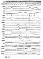
- FIG. 1A is a circuit schematic of a representative detector-preamplifier system which supplies pulses to the present invention;
- FIG. 1B is the trace of a typical detector-preamplifier output signal resulting from the absorption of a single x-ray in the detector;
- FIG. 1C shows a typical output from a continuous discharge detector-preamplifier over the course of multiple x-rays;
- FIG. 1D shows a typical output from a periodic reset detector-preamplifier over the course of multiple x-rays;
- FIG. 1E shows three common x-ray pulse arrival patterns after the ASC has removed the reset-ramp portion of the signal;
- FIG. 2 is a block diagram of the invention showing its major parts and its connections to other equipment;
- FIG. 3 is a block diagram of the Analog Signal Conditioning (ASC) and A to D hardware blocks of FIG. 2;
- FIG. 4 is a circuit schematic of a representative embodiment of several blocks of FIG. 3;
- FIG. 5 is a block diagram of the Hardwired Digital Signal Processor hardware block of FIG. 2;
- FIG. 6A is a circuit schematic of a representative embodiment of the Decimator hardware block of FIG. 5;
- FIG. 6B is a timing diagram illustrating the operation of the circuitry of FIG. 6A;
- FIG. 7A is a circuit schematic of a representative embodiment of the Slow Filter hardware block of Fig. 5;
- FIG. 7B is a timing diagram illustrating the operation of the circuitry of FIG. 7A;
- FIG. 8A is a circuit schematic of a representative embodiment of the FIFO 10 hardware block of FIG. 6A;
- FIG. 8B is a timing diagram illustrating the operation of the circuitry of FIG. 8A;
- FIGS. 9A-9G are a series of timing diagrams demonstrating the relationship between corresponding pulses output by the Fast and Slow Filters of FIG. 5 and illustrating functions of the Peak Detector and Pileup Checker blocks of FIG. 5;
- FIG. 10A is a circuit schematic of a representative embodiment of the Peak Detector hardware block of FIG. 5;
- FIG. 10B is a timing diagram illustrating the operation of the circuitry of FIG. 10A;
- FIG. 11A is a circuit schematic of a representative embodiment of the Pileup Checker hardware block of FiG. 5;
- FIG. 11B is a timing diagram illustrating the operation of the circuitry of FIG. 11A;
- FIG. 12A is a circuit schematic of a representative embodiment of the Input Count Rate (ICR) Counter hardware block of FIG. 5;
- FIG. 12B is a timing diagram illustrating the operation of the circuitry of FIG. 12A;
- FIG. 13 is a circuit schematic of a representative embodiment of the livetime counter hardware block of FIG. 5;
- FIG. 14A is a circuit schematic of a representative embodiment of a Pileup Inspector which measures fast peak widths at their half heights;
- FIG. 14B is a timing diagram illustrating the operation of the circuitry of FIG. 14A;
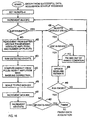
- FIG. 15 is a flow diagram showing the major features of the DSP's control program;
- FIG. 16 is flow diagram of the Data Acquisition Task feature of the DSP's control program; and
- FIGS. 17A-17D are oscilloscope traces of the output of a specific embodiment of the invention ASC showing the effects of time fluctuations in the arrival rate of x-rays;
- FIG. 18 is a block diagram of a control procedure used to keep the ASC's output within the ADC's input range;
- FIGS. 19A-19B are sketches showing the need for pulse height correction terms for two types of preamplifiers.
- FIG. 20 is a sketch defining the terms used in the derivation of the pulse height correction term for the continuous discharge type preamplifier.
- FIG. 21A is a circuit schematic of an alternate embodiment of the Slow Filter hardware block of Fig. 4;
- FIG. 21B is a timing diagram illustrating the operation of the circuitry of FIG. 21A; and
- FIG. 22 shows an alternate Slow Filter embodiment using analog filtering.
-
- The description of specific embodiments will be clarified by a brief discussion of the electrical pulses, corresponding to detected x-rays, which we will process. FIG. 1A shows a common x-ray detector/preamplifier circuit comprising a semiconductor detector diode 10, a voltage supply 12, a charge integrating preamplifier 13 with feedback capacitor Cf 15 and feedback element 17. An x-ray of energy Ex absorbed in diode 10 releases a charge Qx equal to Ex/ε, where ε depends on the diode material. Qx is integrated on Cf 15, producing an output voltage step Vx equal to Qx/Cf or Ex/(εCf), as shown in FIG. 1B. The present invention uses digital filtering to accurately estimate Ex by reducing the noise σ in the measurement of Vx.
- Functionally, there are two basic types of preamplifiers. In the first type, element 17 continuously discharges capacitor 15 (the "CD" case),as by a resistor. FIG. 1C shows a typical CD preamplifier output, comprising a series of signal steps (as per FIG. 1B) with exponential decays between. The average output voltage, Vavg' equals the input diode current Iin times element 17's resistance.
- In the second preamplifier type, element 17 is a switch which closes periodically when the output voltage of preamplifier 13 approaches an upper reset value VU and opens again when the preset lower limit V1 is reached. This is the periodic reset ("PR") case FIG. 1D shows a typical output, comprising a ramp of voltage steps which rise to VU, where reset occurs, returning the voltage VL, whence the process begins anew. The ramp's average slope Savg equals Iin/Cf. Typical signal fluctuations about the average slope are shown in FIG. 1E.
- ADC selection is critical in implementing a digital spectrometer with both good pileup rejection and good energy resolution. Regarding pileup: at least 20 megasamples/second (MSA) is required to achieve 200 ns pulse pileup inspection times.
- Regarding energy resolution: experience shows that to get good energy resolution, the noise range σ (see FIG. 1B) must be about 4 times the ADC's least significant bit ΔV1. This sets the gain (volts/bit) of the amplifier stages preceding the ADC:
- Given ΔV1, the ADC must then have enough bits NB to fully cover the range 0 to Vmax:
- 14 bit ADCs operating at 20 MSA exist, but are expensive compared to the cost of the analog electronics which we want to replace. Fast 8 to 10 bit ADCs, however, are inexpensive due to their wide use in digital communications. In the present invention, we reduce the dynamic range of the preamplifier signal sufficiently to allow the use of these cheaper devices. The reduction from 14-15 bits to 8-10 bits is also advantageous both because shorter words require less electronics to process and because they require less power to process at a given data rate.
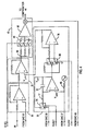
- FIG. 2 shows the basic structure of the invention digital spectrometer. Input from a conventional detector-preamplifier 20, as in FIG. 1A, feeds into a digital spectrometer 22 comprising three functional blocks: an analog signal conditioning (ASC) and analog to digital converter (ADC) block 23; a hardwired digital filter, peak detector, and pileup inspector (FiPPI) block 25; and a programmable digital computer block 27, which in a specific embodiment is a digital signal processor (DSP), for signal refinement, multichannel signal analysis, ASC control and input/output (I/O) functions. The digital spectrometer 22 connects to a general purpose control computer and interface 28, from which it receives parameter values and control signals and to which it sends collected spectra. The function of ASC 23 is not required for the operation of the digital spectrometer blocks 25 and 27, but is our preferred embodiment. The functions of blocks 25 and 27 can be implemented using various circuitry, but in our preferred embodiment are implemented according to the specification presented below. The general purpose control computer and interface 28 are conventional and may include any of a variety of common personal or laboratory computers and interface standards. The details of interfacing a computer to a DSP are well known to those skilled in the art.
- The ASC 23 has two primary functions: reducing the input signal's dynamic range and to adjusting its gain to satisfy Eqn. 1. Dynamic range reduction is accomplished by decomposing the preamplifier signal into two components: a "low frequency'' signal fraction (LFF), of large dynamic range; and a "higher frequency" signal fraction (HFF), of much smaller dynamic range, carrying the signal of interest (SOI; compare FIG. 1D to FIG. 1E). The terms "low frequency" and "high frequency" are descriptive since, in this application, the LFF's fundamental frequency is much lower than the frequency bandwidth carrying the HFF SOI. The important concept is that a reasonable replica of the LFF signal fraction can be described by a relatively small number of parameters, allowing it to be readily generated and subtracted from the input signal. The remainder signal fraction then closely approximates the original HFF carrying the SOI and has a significantly reduced dynamic range, allowing it to be digitized using an ADC with a significantly reduced number of bits.
- Under parametric control by DSP 27, ASC 23 therefore generates a LFF replica, subtracts it from the input signal, and adjusts the remaining HFF replica's amplitude to meet Eqn. 1. Besides requiring fewer ADC bits, this approach has three additional advantages. First, the DSP 27 knows the ASC's control parameters and can use them to refine the energy spectrum it is collecting. Second, since x-ray pulses in the HFF fraction will fall nearly randomly (dithered) across the ADC's input range, the spectrometer 22's accuracy and linearity are relatively insensitive to the ADC's differential and integral non-linearity and completely insensitive to any DC offset voltages. Third, different types of preamplifier input can be accommodated merely by parametric adjustments. For CD preamplifiers, the LFF is merely a constant set to the value Vavg, as shown in FIG. 1C; for PR preamplifiers it is a sawtooth function, consisting of alternating ramps of slope Savg and resets, as shown in FIG. 1D.
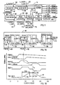
- FIG. 3 is a functional block diagram of ASC and conversion block 23. An amplifier 30 amplifies the difference between the input signal from the detector-preamplifier 20 and a voltage level set by a digital-to-analog converter (DAC) Bias DAC 32 which allows the preamplifier signal to be centered about zero in the rest of the circuit. A subtracter 33 subtracts the output of a LFF generator 35 from amplifier 30's output. LFF generator 35's output waveform is controlled by inputs from an Offset DAC 37, a Slope DAC 38, and a reset line 40 from DSP 27. Subtracter 33's output feeds an amplifier 42, whose variable gain is controlled by a Gain DAC 43. A comparator 44 examines the signal and alerts the DSP 27 on interrupt line 45 if it passes outside the ADC's input limits. A low pass filter 47 removes any signal frequencies above the ADC's Nyquist limit before it reaches an ADC 48.
- The ADC output connects both directly to FiPPI block 25 via a digital ADC output bus 50, and indirectly to DSP block 27 via the bus buffers 52. The buffers 52 attach to the bidirectional DSP data bus 53, the DSP address lines 54, and the reset line 40 and allow DSP 27 to load digital input values to the DACs 32, 37, 38, and 43. and sample the ADC output data stream on ADC output bus 50 as desired. Thus DSP 27 both directly controls all the ASC 23's functions and can also directly measure their effects on the ADC output 50. With appropriate control software, this allows DSP 27 first to initially set preferred operating values for the ASC 23 and then to dynamically control the LFF generator 35's operation as well. The details of using interface buffers are well known to those skilled in the art of digital electronics and will not be described further.
- Under DSP 27's control, LFF generator 35 generates a resetting ramp function with a DC offset. For a CR preamplifier only a DC offset of value Vavg is used (see FIG. 1C) . For a PR preamplifier, the DC offset is set to the value VL and the ramp's slope is adjusted to match the average slope Savg (see FIG. 1D). Three PR output signal samples, after ramp subtraction, gain adjustment and filtering, are indicated in FIG. 1E. After removal of the quasi-periodic ramp structure, the individual x-ray pulses appear as vertical steps with fluctuations in their arrival times. Trace A shows an average rate of arrival case. Traces B and C show temporary fluctuations from the average. Ramp subtraction leaves a negative slope between steps, but their amplitudes are not appreciably modified by this procedure and are to be recovered by the digital spectrometer.
- For CR preamplifiers, the ASC output would look much like FIG. 1C, except that the vertical scale would be adjusted to fill the ADC's entire input range. In this case the regions between the x-ray pulses have the same exponentially decaying slopes as the preamplifier.
- FIG. 4 is a circuit schematic of the amplifier 30, subtractor 33, LFF generator 35, and variable gain amplifier 42 blocks of ASC 20. The circuit will be self explanatory to those skilled in analog electronics and needs little further discussion beyond a few design comments. Circuit details which are well known to those skilled in the art, such as power supply filtering or op-amp compensation, are not shown. The implementation are not unique and many other suitable arrangements can be readily devised.
- Beyond centering the input signal in the ASC circuit's range, the primary function of amplifier 30 is to buffer the ASC from the input and ease noise requirements in the rest of the circuit by amplifying the input by a factor of about 3. It should therefore be implemented using a very low noise op-amp of adequate bandwidth.
- The LFF generator 35 is a resettable current integrator, with offset voltage Voff' designed to generate low noise, high accuracy ramps with settling times of less than 5 µs on reset. Resistor 68 converts a current from DAC 37 into voltage Voff. Capacitor 72 integrates a current from DAC 38 until reset by switch 75. Resistor 77 assures that the slew rate of PET op-amp 65 is not exceeded. Op-amp 78 and switch 85 allow the amplitude and sign of LFF generator 35's output to be matched to the input. DAC 37 is usually adjusted so that the LFP generator 35's output and the signal from amplifier 30 match immediately after preamplifier resets.
- The variable gain stage 42 comprises a switch 88 and resistors 90 for coarse gain into the 100 ohm fixed input impedance Analog Devices AD603 92, a voltage controlled, variable gain op-amp for fine gain. To minimize noise, the fixed output noise op-amp 92 is only used for fine gain adjustments of about 12 dB.
- The remaining blocks in the ASC section 20, a comparator 44 and a low pass filter 47, are straightforward to implement. The comparator is required to detect any occasions, see FIG. 1E, when fluctuations cause the ASC output signal to exceed the range LL to UL which is mapped onto the ADC's input range.
- The low pass filter 47 limits the ASC output signal's bandwidth to less than the Nyquist frequency, f N, which is half of ADC 48's sampling frequency, because all noise at higher frequencies will be "aliased" into the digitized output signal, unnecessarily increasing its noise. In this specific embodiment, the ADC operates at 20 MHz so f N is 10 MHz. While various filter designs could be employed, a 4-pole Butterworth filter is used in the specific embodiment because it has fast rolloff in frequency, minimum peaking in time and requires only four passive components. We have experimentally verified that, when the Nyquist criterion is met, spectrometer energy resolution is independent of sampling rate: embodiments operating at 2, 5, 10 or 25 MSA, with lowpass filters of 1, 2.5, 5 and 12.5 MHz respectively, all produced identical energy resolution for triangular filtering with 2 µs peaking time, even though the number of data samples collected in these cases varied from 8 at 2 MSA to 100 at 25 MSA. The several authors who have reported improvements in energy resolution with increased sampling rates have clearly failed to satisfy the Nyquist criterion. Selecting a sampling rate is therefore primarily a tradeoff between raising sampling rate to achieve good pulse pair resolution and lowering sampling rates to lower digital processing costs.
- As discussed in the summary, the invention spectrometer carries out digital filtering in two stages. The first stage, designated the FiPPI, uses combinatorial logic to implement Filtering, Peak detection and Pileup inspection. In order to minimize filtering circuitry and maximize processing speed, no more complex operations than addition and subtraction are allowed in this stage. To optimize speed, all operations are pipelined to process input data at one point per clock cycle. Thus, if O(n,j) is the jth operation required by data sample n, then at time step i, we simultaneously execute operations O(n,1), O(n-1,2), O(n-2.3), etc.
- This approach has significant limitations because compensatory adjustments cannot be made based on pulse-specific conditions and filters using only addition or subtraction are not accurate enough to meet our spectroscopic performance goals. Thus, as noted in the summary, in the second filtering stage a DSP is employed to make the specific corrections (based upon preamp type, local operating conditions, etc.) required to achieve the desired accuracy.
- This approach is advantageous for several reasons. First, the FiPPI can be both very cheap and very fast. For example, in the preferred embodiment, it is implemented in a single FPGA while running with a 20 MSA ADC. Second, the functions in the second step are only executed at the x-ray signal events' average arrival rate, which is much slower than the ADC sampling rate (e.g., 500,000 cps compared to 20 MSA) . Because the required corrections are typically simple formulae, applying them only to captured peak values is both simpler and faster than making them on the data stream itself (through preconditioning or deconvolution), as practiced in existing art. In the same embodiment, only a 20 MIP DSP is needed for second stage processing.
- The FiPPI in the specific embodiment therefore implements only trapezoidal filtering, including triangular filtering as a subset. This choice does not degrade the spectrometer's energy resolution in the high count rate regime contemplated because, as Gatti and Manfredi showed in their paper entitled ''Processing the Signals from Solid State Detectors in Elementary-Particle Physics'' published in Revista del Nuovo Cimento (1986) Vol. 9(1), pp. 1-146, triangular filtering is actually the ideal fixed shaping form in the short shaping time regime where series white noise dominates. Even at longer shaping times the triangular shape is still very effective: Radeka showed in his paper entitled "Low Noise Techniques in Detectors", published in Annual Reviews of Nuclear Particle Science 38 (1988), pp. 217-277, that even for maximum energy resolution a triangular filter's resolution is only 8% worse than an ideal cusp filter.
- In one specific embodiment, the FiPPI logic is implemented using a field programmable gate array (FPGA). This allows a high logic density in a small space. Further, because the FiPPI's logic is downloaded from a file prior to operation, it can be readily modified, either to meet new conditions or to incorporate design improvements. In other embodiments, where lower costs or higher operating speeds are desired, the FiPPI can be implemented with an application specific integrated circuit (ASIC) or other logic circuitry.
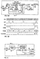
- The topology of the FiPPI 25 in a specific implementation is indicated in FIG. 5. The data stream enters on ADC output bus 50 and feeds into both a slow and a fast signal channel. The first slow channel circuit, a decimator 97, reduces the incoming signal's data rate by a preset factor. Its output is processed by a slow filter 98 which digitally implements trapezoidal filtering. Peak maxima in slow filter 98's signal output correspond to the energies of detected x-rays and can be captured by an output buffer 100. The operation of the slow channel is controlled by three parameters loaded into FiPPI 25 from DSP 27: a decimation factor 102 and the slow filter's length and gap values 103.
- The fast signal channel's principal function is to inspect the data input stream 50 and trigger output buffer 100 to capture appropriate values from the slow filter 98. The first fast channel circuit is a fast filter 105, which also digitally implements trapezoidal filtering, but with a much shorter time constant than in the slow channel. A peak detector 107 inspects its output for peaks which exceed a preset threshold value for at least a preset number of consecutive samples and then captures the arrival times of these peaks' maxima. These arrival times define the associated x-ray events' arrival times and are used to time the trigger to the output buffer 100. Output pulses from the peak detector are inspected by a pileup checker 108 which rejects events whose maxima would overlap (pile-up) in the slow filter 98. Each time the pileup checker 108 detects a good peak it triggers output buffer 100 to capture the slow filter's 98 output value for export to the DSP 27 for second stage processing. Each peak detector 107 output pulse also increments an input count rate (ICR) counter 110. As in the slow channel, the fast channel's operation is controlled by parameters loaded from the DSP 27: the fast filter length and gap 112, the peak detector's threshold and minimum peak width test values 113, and the interpeak interval, fast peak maximum width, and timing offset values 115 required by the pileup checker.
- Each time output buffer 100 is triggered it also captures two other values: the value in ICR counter 110 and a flag to denote what type of slow filter value was captured. The buffer therefore outputs four values to the DSP 27: two captured slow filter values PKVAL 117 and UFVAL 118, the number of x-rays PLOUT 119 since the last output, and a flag BLFLG 120 indicating whether PKVAL 117 is an x-ray amplitude value or a baseline value for normalization purposes.
- The FiPPI's final circuit is a livetime counter 121, which measures the actual time TIME 122 the digital spectrometer spends collecting data. This is useful for two reasons. First, it is otherwise difficult to precisely time data collection processes started under software control by control computer 28. Second, in a multiple detector system it is important for each spectrometer to be able to accurately measure its own livetime so that its count rates can be accurately determined.
- The implementation and operation of the subcircuits in the FIPPI preferred embodiment are shown by the circuit schematics in Figures 6 through 13 with their accompanying representative signal traces. These circuits and traces will be largely self explanatory to those skilled in the art of digital electronics. In the following paragraphs we will primarily relate their functions and indicate any design issues which are not obvious
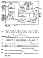
- Fig. 6A is a circuit schematic of the decimator 97, with representative signals shown in FIG. 6B, of a specific embodiment hardwired to decimate by 4. It comprises a clock divider 123 and an N value summer 125, which adds four consecutive values from 10 bit input line ADCBUS 50 and outputs their sum on the 10 bit line CS 147. If more accuracy is desired, more bits may be retained in CS. Using similar techniques, circuits which decimate by any arbitrary parameter D_Factor 102, may be readily built.
- The trapezoidal filter function values {Ti} of a stream of data values {di} at times {i} are given by the equationHere L and G are the slow filter interval length Ls and gap interval Gs and enter the module as Parameters 103. When the Gs is zero, a triangular filter function is obtained. Both forms have been extensively discussed in the analog spectrometer literature. The trapezoidal function's amplitude can be made independent of charge collection time if the gap Gs is adequately long, thus avoiding the phenomenon of ballistic deficit. Its signal to noise ratio for short shaping times is not as good as the triangular function's, however. In the present case the choice is set by the parameters S_Length and S_Gap 103.

- To avoid long summations which consume excessive FPGA real estate and also operate slowly, Eqn. 3 can be recast as:
- The circuit schematic in FIG. 7A and the waveforms in FIG. 7B describe an implementation of the slow filter module 98.that creates Ti values according to Eqn. 4 for a 10 bit input. The width of all the components in the filter would expand by 1 bit for each bit of decimation. The input CS[9:0] 147, from the decimator 97, has a slight slope both before and after a typical pulse to represent the effects of detector leakage current and/or the operation of the ASC 23.
- FIFO memory 148 and subtracter 150 create the terms (di-di-L), where L is set by parameter PA[4:0] 152. FIFO memory 158 and subtracter 160 create the terms (di - di-L) - (di-L-G + di-2L-G), where L+G is set by parameter PB(4:0] 162. Accumulator 168 then creates the values Ti of Eqn. 4 on line FS[11,0] 173. Pipeline delays of 3 clock cycles are produced. The use of 12 bits in accumulator 168 is just an engineering tradeoff for XAS applications where only a narrow range of x-ray energies is expected and the ASC gain can be optimally set so one x-ray step is about 5% of the ADC input range. In a more general design an increased number of accumulator bits would be advantageous.
- Thus a step function in C[9:0]) P[11:0] becomes a trapezoidal pulse whose rising and falling times 175 and 177 both equal the ''peaking time" TPK, which equals L. Its flattop 178 has duration TGP, the "gap time," which equals G the difference between PA 152 and PB 162. The black dot on trace FS[11:0] in FIG. 7B shows the time tm when the pileup checker captures FS[11:0] to output buffer 100 if the peak is not piled-up. When CS[9:0] is also captured, this happens 3 clock cycles earlier to account for pipeline delays.
- The output FS[11:0] 173 has a non-zero baseline which is proportional to the slope in signal CS[9:0] 147. Thus, peak amplitudes must be measured with respect to the baseline, which must therefore also be determined accurately. Also, when the slope in CS[9:0] is not constant in time (as for a DC preamplifier), then the baseline will have to be measured locally for each detected x-ray pulse.
- The combination of decimator 97 and slow filter 98 allows peaking times of up to 400 samples (20 µs for a 20 MSA ADC) using FIFOs which are only 32 deep and a 12 bit accumulator, whereas a direct implementation would require 400 deep FIFOs and an 18 bit accumulator. Not only does this require fewer FPGA gates, but shorter word lengths allow the circuit to run fast enough using a cheaper grade FPGA than would otherwise be the case.
- FIGS. 8A and 8B show a circuit and waveforms of a specific implementation of FIFO 148, using a Xilinx 4000 series FPGA for Ls equal to 3. The other FIFOs in the design are implemented similarly. Ten 32 bit deep memories (one per data bit) are cyclically addressed by a cyclical address counter 185, whose output QC is out of phase with the clock 128. The Xilinx memories therefore display their stored data 0[9,0], which are captured by buffers 188, when first addressed by QC. These values are then overwritten by new values of C 147 as the clock goes positive. Thus a read and a write are accomplished in a single clock cycle, with the output values delayed from the input by PA 152 counts.
- The fast filter 105 is implemented in exactly the same way as the slow filter except that it has its own control parameters F_Length and F_Gap 112 and works directly with the 10 bit output 50 of the ADC 48. Its peaking time and gap length, from Eqn. 4 are written as Lf and Gf, the subscript f signifying "fast."
- To understand pileup inspection, one must understand how the slow filter 98 and fast filter 105 pulse outputs change as a function of the time interval between consecutive input pulses FIGS. 9A-9G present this information, showing superimposed fast filter 192 and slow filter 193 output traces as the time between two input pulses decreases. Provided the two peaks are adequately separated (FIGS. 9A-9C) the amplitudes of the slow filter peaks remain valid measured of the x-ray energies. At shorter times these peaks merge and must be rejected. The minimum.allowed separation is when the second pulse begins (corrected for pipeline delay) one clock cycle after the first peak is sampled. Otherwise the two pulses are piled up. As the interval between the pulses continues to decrease, the fast pulses will also eventually overlap, and pile up as well (FIGS. 9E-9F).
- The first issue is to detect pulses which is the function of the peak detector 107. The preferred implementation offers improved performance over classical discriminators which have timing jitter and do not operate well for pulse amplituded close to the noise floor. Here, as shown by the circuit and traces in FIGS. 10A-10B, a threshold level 195 is set by a parameter PC 207. However, signal values FF 205 are only recognized as a peak when they exceed the threshold at least a minimum number min_width 113 (set by parameter PD 208) times in a row. Under this condition the signals RFP 223 and SFP 225 are generated. RFP lasts as long as FF continues to exceed the threshold. The values of both the threshold 195 and min_width 113 may be adjusted to increase noise immunity when working with soft x-ray pulses which do not rise far above the noise floor.
- The second issue is to determine pulse arrival times, which is the function of Block 240 of Pileup Checker 108, as shown by the circuit and traces in FIGS. 11A-11B. Here the fast peak's location is determined not by its crossing of threshold 195, but by the time T3 196 of its maximum value. Whenever RFP 223 is high, this block compares FF 173 to previously captured maximum values in buffer 250, setting FTOP 255 high each time a new maximum is found. Arrival time locations TS 196 are now essentially amplitude independent, greatly reducing time jitter and removing any energy dependent skewing of slow channel peaks amplitude determinations.
- Once a peak is detected, the FiPPI must determine if it is free of pileup and, if so, capture its amplitude in the slow channel. The actual capture is carried out by the Output Buffer 100, which is shown in more detail in FIG. 11A and is triggered by the signal PSAM 298. The timing of slow peak amplitude capture is conceptually straightforward, as shown in FIG. 9A. The desired capture time T4 198 is at the trapezoid's flattop midpoint. Because the digital processing operations in both fast and slow channels are fixed in number, T4 198 is separated from the fast peak's arrival time T3 196 by a constant time TS 194, which depends only on such FiPPI control parameters as D_Factor 102, S_Length and S_Gap 103, and F_Length and F_Gap 112. Thus, following fast peak detection, a counter can measure time TS 194 and transfer the slow filter 98 output transferred to buffer 100.
- The pileup inspection implemented digitally in the FiPPI is conceptually similar to that commonly found in analog spectroscopy circuits: requiring that successive pulses must be separated by some multiple of the slow channel peaking time. In the case of analog triangular filtering, a multiple of 1.5 - 2.5 is commonly used. As FIG. 9A shows, for truly trapezoidal filtering, successive pulses need only be separated by a single slow filter peaking time plus half the flattop time. The fact that analog ''triangular'' pulses have tails that extend significantly beyond one peaking time on the decaying side of the peaks is the source of their extended inspection times. Digitally generated pulses terminate cleanly, as shown in FIG. 7B, allowing shorter pileup inspection times to be used. Resulting increases in count rate capability of 2 or more have been demonstrated.
- The trailing edge pileup inspection is carried out by block 243 in the circuit shown in FIG. 11A with traces shown in FIG 11B, which measures the time intervals between adjacent terminations of the signal FTOP 255. A falling FTOP signal, which marks a fast peak maximum and thus its arrival time, starts the Interval_1 Counter 260, which is loaded with the parameter PF 268, the pileup inspection period. If the counter overflows successfully and the value stored in FF16 265 shows that the pulse does not have leading edge pileup, then a signal is issued to a second interval counter block 245 which finishes counting the time TS 194 at which the slow channel peak should be captured. The Interval_2 counter is required to accommodate pipeline delays in the slow filter, which may be running with a decimated clock.
- When Interval_1 counter 260 overflows, it is restarted and Pass_Cnt counter 261 is incremented. If Interval_1 counter 260 overflows a second time, it means that the interpulse period has been long enough for the slow filter output to return to baseline. Under this condition, if the DSP 27 has set the flag BLCOL 315, then Interval_2 counter 245 will be triggered to initiate a baseline capture. The bit BL 278 is captured by buffers 100 as the output value BLFLG 120 to signify this condition.
- Whether or not a peak is free of leading edge pileup is determined by flipflop FF16 265, which stores the value of Pass_Cnt counter 261 each time a new fast pulse is detected, as signaled by the signal SFP 228. If this value is 1, then a time of at least PF 268 has passed since the last pulse.
- When the unfiltered output CS (see FIG. 7B) is required, it must be captured 3 slow clock cycles before time T4 198, which is before Interval_1 counter has actually determined if the peak will be valid. This time is therefore determined by comparator CMP23 262, which causes the appropriate value of CS to be captured to an intermediate buffer 307, where it can be transferred to Output Buffer 100 if the peak is valid.
- A first fast pileup test is implemented by block 242 in FIG. 11A, which measures the width of the fast pulse a the threshold value 195. As FIGS. 9E-9F show, if this value TW is more than a maximum value TM 200, then there must be pileup in the fast channel and the slow channel peak value will be invalid. This result, when detected, is stored in flipflop FF16 265, which prevents the slow peak capture. Because both the parameter TM and the threshold can be adjusted on a case by case basis, this is a very effective test when coupled with our fast peak detection circuit. With quasi-monochromatic x-rays, as in XAS, the parameters can be tuned to achieve pileup rates which can be up to 3 orders of magnitude lower than with conventional analog tests.
- The circuit and traces in FIGS. 12A - 12B show an embodiment of the FiPPI 15 input count rate counter 110 (see FIG. 5) . This circuit uses the fast pulse arrival signal SFP 228 and the output Q10[0] 270 of Pass_Cnt counter 261 to record the total number of x-ray pulses detected for each valid x-ray pulse detected. Its output NSFP 340, can be read by DSP 27 at the same time as it reads buffers 100.
- The circuit in FIG. 13 shows an embodiment of the FiPPI 15 live time counter 121 (see FIG. 5). This circuit counts a divided clock signal at all times that the DSP 27 signals, via C_Enable 373, that it is in data collecting mode.
- A second fast pileup test can be additionally implemented according to the circuit and traces shown in FIGS. 14A - 14B. This circuit measures the width of the fast peak at one half of its maximum. Other ratios could be readily substituted. The Inspect_1 counter sets the inspection period PL 362 while the Half_Width counter 357 compares the peak width to the maximum allowed value PK. The fast pulse signal FF 173 is delayed PJ 358 counts by FIF010 353 until Q7 251 has a chance to attain its maximum value. If the fast peak is piled up according to this test, output MWID1 367 can be used to set flipflop FF16 265 to prevent the slow peak capture.
- This test works particularly well when pulses with a wide range of amplitudes are present, preventing the fast pulse and pileup tests to be optimized for low amplitude pulses where the threshold may be a sizable fraction of peak amplitude. In this case there may be quite a wide range of times over which two low amplitude pulses can pile up and still have the sum of their two widths be less than the base width pileup test value.
- Although the circuitry is not shown in this specific implementation, we have found it to be advantageous, in systems designed for the highest counting rates, to replace the three output buffers 100 by three short FIFOs, each capable of storing several captured values. This modification allows the DSP 27 more flexibility in how it collects captured peak values from the FiPPI. In the preferred implementation shown, the DSP operates under interrupt control, pausing in its computations to fetch a captured value in less that 0.5 µs each time one is signaled. While this system uses fewer FiPPI circuit resources, it requires more, and on average slower, DSP code to service the interrupt routines. With the optional FIFO output, the DSP can poll the FiPPI for data at a fixed point in its processing routine and never be interrupted, which increases its average processing speed. This implementation is therefore preferred when the very highest data rates must be accommodated.
- We have modeled this operation and found that, if the DSP 27 polls DSPFLAG 302 at least once per event it processes, and is fast enough to process events at their average rate, then this buffer need only be about 4 events deep to capture the vast majority of all events.
- In accordance with our design philosophy, the DSP carries out those tasks, procedures, and computations which are required either on a "per event" basis or less often, to maintain system level operations. As shown in FIG. 2, the DSP 27's major tasks include interacting with the general purpose control computer and interface 28, adjusting and controlling the ASC 23, and collecting, correcting and histogramming data values from the FiPPI 25. In the general practice of the invention, these functions could be met by a wide variety of combinations of processor and memory, the choice in any particular embodiment being primarily an engineering decision based on such considerations as cost, speed, size, and so forth.
- An NEC µPD77016 processor is used in the specific embodiment. It was selected because it is a fast, low cost, 16 bit DSP with enough internal memory to hold both its control program and the spectra produced by its MCA function. Its 2.0 K X-data memory is dedicated to MCA spectra, allowing spectra to be histogrammed into up to 1024 bins, each 32 bits (or more than 4 billion counts) deep. Its 2.0 K Y-data memory stores the variables and constants required to control system operation; data to monitor system performance; and a circular buffer to temporarily store FiPPI events for MCA processing. Internal memory is not necessary for the invention but reduces total package count and cost and may allow higher speed operation. Executing instructions at one half its externally applied clock frequency, the DSP is clocked at exactly twice the rate of the ADC and FiPPI, to produce synchronous operation of one instruction per ADC sample. It has 4 external interrupt lines, which allow it to respond to the ASC 23, FiPPI 25, and external control computer 28.
- The general issues associated with programming and interrupting microprocessors and DSPs are well known to those skilled in the art and will not be described in any detail. General flow charts of the control programs will be shown and attention will concentrate on the specific algorithms which have been invented to produce the desired instrument function.
- FIG. 15 shows a high level flow chart of the supervisory control program used in the specific embodiment. Bold arrows trace the flow of program control through a single data collection cycle. Operation begins by downloading the DSP's program and Initialization 380, including setting up registers and initializing constants in Y-data memory. The program then proceeds to its primary control loop, the CAMAC Monitoring Task 382. In the specific embodiment the control computer interface was implemented using the CAMAC interface standard, IEEE Standard 583-1975, but this choice is not critical to the invention's function. In the CAMAC Monitoring Task 382 the DSP is essentially in a loop, waiting to be interrupted.
- Data transfers to and from the DSP are initiated by the control computer 28 through its interface to the digital spectrometer 22. The details of implementing such interfaces are well known to those skilled in the art. These requests for data transfer cause the interface to generate a Transfer Interrupt 383 to the DSP. When such a Transfer Interrupt 383 is received, the DSP moves to Transfer Data To/From DSP 385. Here it reads two status registers in the interface 28 and uses their contents to determine whether it should transfer a data word to a DSP memory location from an interface register or vice versa. It makes the requested transfer and then to the CAMAC Monitoring Task 382. Multiple word data transfers are similarly implemented using the DSP's block data transfer mode at rates up to 2 MBytes/second.
- Before the digital spectrometer 22 can be controlled effectively, it requires the values of various constants and control parameters which must either be downloaded from the control computer 28 (e.g., the FIPPI 25 filter lengths) or be determined experimentally (e.g., a Slope DAC 38 estimate) by calibrating the system. Of particular note is the control word RUNTASKS, which is a set of flags to control DSP program flow. When an Acquisition Interrupt 387 is received. Acquisition Type 388 is determined by testing RUNTASKS.
- If Acquisition Type is Test/Calibrate 390, the DSP executes Test/Calibrate Routines 392, which are used to verify correct system operation and calibrate the DAC controls to the ASC. They include:
- 1) Write to Bias 32, Offset 37, Slope 38, and Gain 43 DACs to set the operating point of the ASC 23.
- 2) Measure overall system gain by first disconnecting the input to spectrometer 22 and then recording the output of ADC 48 for a series of voltage values applied to Op Amp 30 using Bias DAC 32. A fit to the results yields ADC units per Volt input, which is just the digital spectrometer's gain. This can be multiplied by the preamplifier gain in Volts per eV of x-ray energy to obtain overall system gain in ADC steps per eV. If the preamplifier gain is not known, a measurement of a known x-ray energy can be made to provide this constant.
- 3) Calibrate Offset DAC 37 in ADC units, by the same process as in routine 2) above, to obtain the normalization constant DACperADC, the number of Offset DAC steps required to change the ADC output by one step.
- 4) Calibrate the slope generator by setting known values into the Slope DAC 38 and measuring the time required for the generated signal to go out of the ADC input range. Slope depends only on the current input from Slope DAC 38 and the size of the integration capacitor 72, thereby providing a good secondary test of the DACperADC value.
- 5) Test ADC differential and integral non-linearity using the ASC's slope generator as a controlled input waveform.
- 6) Monitor ASC interrupts without acquiring spectrum data.
- 7) Capture ADC output signal traces with DSP. This mode, in which the ADC-DSP combination essentially operates as a simple digital oscilloscope, can be particularly useful for debugging detector problems by allowing representative signal traces to be captured.
- 8) Capture FiPPI Decimator output values C[9:0) 147. This has the same utility as routine No. 7, but works with the slower Decimator output.
- 9) Verify correct operation of the entire spectrometer by first disconnecting the spectrometer's 22 input and then collecting a spectrum using voltage steps output by Bias DAC 32 to simulate input x-ray signals. The output spectrum should be a single narrow peak whose location is a direct measure of the overall system gain and whose width measures the spectrometer's noise. This test is a valuable diagnostic that the complete instrument is operating correctly for the selected digital filter parameters.
-
- These tests allow the invention digital spectrometer to be both self testing and self calibrating and are also useful for quality control tests in manufacturing. In normal operation, the control computer 28 runs a test suite of these programs to assure that the spectrometer is operating correctly prior to attempting to collect data.
- When the Acquisition Interrupt Type is Data 393, then the DSP moves to the Start Data Acquisition Routine 395 and executes the following tasks to prepare for data acquisition (assuming a reset type preamplifier) .
- 1) Set the ASC's Bias DAC 32, Offset DAC 37, Slope DAC 38, and Gain DAC 43 to specified values determined by the x-ray energy range, characteristics of the preamplifier, and initial rate estimates.
- 2) Reset the MCA data and statistics to zero.
- 3) Write control parameters Decimation Factor 102, Slow Filter Length and Gap values 103, Fast Filter Length and Gap 112, Peak Detector Test Values 113, and Pileup Checker Values 115 to the FiPPI and restart FiPPI operation.
- 4) Initiate ASC monitoring by observing ADC values versus time, with the slope generator disabled. Estimate ramp slope in the preamplifier signal and compute a Slope DAC 38 value to match it. Then load the reset value into Offset DAC 37 and enable the slope generator 35.
- 5) Enable the ASC Comparator Interrupt to interrupt the DSP if the ASC's 28 output signal exceeds the ADC's 48 input range.
- 6) Collect an initial set of slow filter baseline values and compute baseline mean and variance.
- 7) Set up pointer values to a circular event loop buffer in DSP Y-data memory to prepare for receipt of FiPPI data.
- 8) Enable PiPPI interrupt signal DSPFLAG 302 allowing the FiPPI to signal the DSP when it captures a valid peak amplitude.
-
- If any of these procedures fail, the program aborts, otherwise it proceeds to Data Acquisition Task 402. This task is designed to accommodate bursts in data arrival rate up to 2,000,000 cps (which is the inverse of the minimum 0.5 µsec slow channel peaking time) while processing data at average rates of up to 500,000 cps. This is accomplished by storing incoming data in a circular buffer, which is a fast process under interrupt control, and processing them at a steady rate in the intervals between interrupts. This reduces the average processing rate by a factor of about 4 and allows the use of a much less expensive DSP.
- Capture FiPPI Data Routine 405 carries out the data capture step. Here the DSP reads two 16 bit words from the FiPPI containing the values PKVAL 117, UFVAL 118, BLFLG 120, and PLOUT 119. It then writes these two words onto the circular buffer, and increments the pointer to their address. These operations require only 5 or 6 clock cycles. Control then returns to the Data Acquisition Task 402 to processes any data remaining in the circular buffer. This continues until either a preset maximum number of events are processed or until a Stop Data Acquisition 407 occurs. In either case, the program proceeds to Finish Data Acquisition 408, whose primary functions are to disable the ASC Comparator Interrupt 45, disable the PiPPI interrupt 302, finish processing any remaining data in the circular buffer, and record the value in the livetime counter 121. The program then returns to the CAMAC Monitoring Task 382, where the collected data can be unloaded.
- The Data Acquisition Task 402 can also be interrupted by ASC Interrupt 410 at any time the ASC 23 output exceeds the input range to ADC 48, forcing a branch to the Fix ADC Out of Range Condition 412 routine, as described below. Once correct ASC operation is restored, the program returns to processing data in the circular buffer.
- FIG. 16 shows a flow chart of a specific embodiment of the Data Acquisition Task 402. For the most part, this chart will be self explanatory to those skilled in control computer programming. Beyond general comments, our discussion will center on the steps which are unique to the invention spectrometer function. The program is essentially a loop which processes date from the circular buffer until it is halted either because test NEVENTS = MAX? 463 is true or until an appropriate value of RUNTASKS is found in the test RUN ENDED? 440. Once every 256 times around the loop and independent test of the ADC condition is performed and a baseline estimate is collected from the slow filter to UPDATE BASELINE ESTIMATE 438, which will be discussed further below. The number 256 is not critical and was selected so that the baseline would be updated often enough to track changing experimental conditions but not so often that it represents a substantial computation burden within the Data Acquisition Task 402.
- In the processing loop, once data from a good event have been read from the buffer 452, the total number of events is incremented 453 using the value PLOUT 119. Total counts can be divided by the recorded livetime to obtain a true Incoming Count Rate estimate. Statistics on PLOUT values can also be collected and used to monitor for incorrect experimental conditions such as excessive flux. The DSP then performs the computations and corrections, for distortions from the ASC 23 and otherwise, required to compute an accurate x-ray energy 455 from the captured slow filter values PKVAL 117 and UFVAL 118. The algorithms selected must be appropriate for the detector-preamplifier combination to which the invention spectrometer is connected. This is an inventive step and will be described further below. Once the energy has been found, it can be scaled to compute a multichannel analysis (MCA) bin 458 and that bin incremented 460 to generate a histogram of the detected x-rays' spectrum using techniques well known to those skilled in the field.
- Because the present invention digital spectrometer system comprises three linked modules: the ASC 23, FiPPI 25 and DSP 27; several novel algorithms are required to control them effectively. These will be described in the following sections.
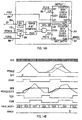
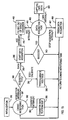
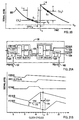
- The essence of this problem is that fluctuations in input counting rate can cause the output of the ASC analog subsection 23, which is the amplified difference between the preamplifier input and the LFF function generator 35, to temporarily fall outside the input voltage range to ADC 48 (i.e., the range LL to UL in FIG. 1E). This is illustrated by FIGS. 17A and 17B. FIG. 17A shows the most common cases, where temporarily high rate (trace B) or low rate (trace C) return to the average rate (trace A). Because x-ray arrivals are truly random, however, some small fraction of cases will appear as in FIG. 17B, where high (trace D) or low (trace E) arrival rates persist long enough to exceed the ADC's input range LL to UL. This invalidates the FiPPI's 25 data stream, requiring the DSP 27 to take corrective action. It does so by adjusting the signals to LFF generator 35 control DACs 37 and 38 until the ASC's output signal returns to the ADC's input range. FIGS. 17C and 17D show two examples where DAC 37 is adjusted. The types of fluctuations which are commonly encountered include preamplifier resets, cosmic ray events in the detector, and statistical fluctuations in the rate of arrival of x-rays to the detector.
- The algorithm shown in FIG. 18 is designed to deal with these situations in a rapid and efficient manner and, in the preferred implementation, typically restores proper operation in less than about 2 µs. With the following few comments, this algorithm will be clear to those skilled in computer programming. The action boxes "Move Down 1" 495 and "Move Up 1" 504 refer to adjustments by DAC 37, where a ''unit" step is the number of DAC bits required to move half way across the ADC input range, as shown in FIGS. 17C and 17D. The box "Reset" 49B means that a preamplifier reset has been detected and requires the LFF generator 35 to be reset as well, using switch 75 and returning DAC 37 to its standard value. The box "If ABS(FLAG) = 1, Update Tracker" 511 means that a simple drift out of range was detected, as shown in FIG. 17B, and the slope tracking algorithm described in the next section should be invoked.
- When Slope DAC 38 is set correctly, then, on average, out-of-range excursions should be equally likely in the Hi and Low directions. But if the incoming x-ray rate changes, then the Slope DAC will need to be adjusted. Therefore, each time the program calls the Fix ADC Out-of-Range Condition 412 routine it notes whether the excursion was in fact Hi or Low and determines whether the Slope DAC setting needs to be adjusted.
- Thus, each time 'Update Tracker" 511 is called, a weight w is updated which, in the specific implementation, has an exponentially decaying memory of past Out-of-Range conditions, according to the formula
- Some computation is required to convert the FiPPI 25 output value PKVAL 117 to an x-ray energy without introducing systematic errors, primarily because the regions just before and just after the x-ray step in the ASC's 23 output are not flat, as in FIG. 1B, but are tilted, as in FIG. 1E. There are two contributions to this tilt for periodic reset preamplifier:.first, because the ASC 23 has subtracted off the ramp generated by the LFF generator 35; second, because of leakage currents from either the detector or the preamplifier's first FET.
- The PiPPI's 25 response to this sloped signal is indicated in FIG. 19A (for the PR preamplifier case). While the amplitude A is desired, the FiPPI produces the value H, which is the difference between the two shaded regions above and below the edge. Computation is therefore required to recover A from the measured value H. FIG. 19A shows that, for a slow filter length Ls with a gap time of Gs:
- We thus wish to obtain a precise estimate of the second term, which would otherwise degrade the spectrometer's energy resolution. Ls and Gs are parameters and are known exactly, as is the generated slope Sg. S1 must be measured, which can be done using measurements according to Eqn. 7 when A equals 0, i.e., when no x-ray events are present anywhere within the filter. Now H equals -(Sg - S1)(LS+GS) and is the ''baseline'' between triangular pulses. By making many measurements, we can estimate the mean baseline value B to arbitrary precision:
- The baseline B must be determined with sufficient accuracy so that it does not affect the spectrometer's resolution. Since, in Eqn. 9, the variances σP and σ B of PKVAL and B add in quadrature, σ B should thus be of order 1/10 σ P and B should be determined from an average of approximately 100 measurements of PKVALB, assuming Gaussian distributed errors.
- The determination of B in the preferred embodiment proceeds in two steps. First, in task no. 6 of the Start Data Acquisition Routine 395, 100 measurements of PKVALB are made and then their average B and variance σ B are computed. This provides an accurate starting value of B. Second, in Data Acquisition Task 402 (FIG. 16) B is updated once every 256 loops in procedure Update Baseline Estimate 438. While various running averages of B could be computed, in the specific embodiment.
- For a CD preamplifier, the signals on both sides of the x-ray step event are decaying exponentials with different average slopes, as shown in FIGS. 19B and 20. The situation is therefore more complex than for a PR preamplifier and requires a modified algorithm to replace Eqn.9. No changes in either spectrometer hardware or FiPPI firmware are required, however.
- FIG. 20 shows the situation. We desire amplitude A, but capture value H, the difference between the running averages <V2>, captured 0.5(LS+GS) after the pulse, and <V1>, captured 0.5(Ls+Gs) before the pulse. S2 and S1 are the signal slope at the two measurement points, Ve its value at time te instantaneously before the x-ray event, and V0 the value to which it decays exponentially. We define the constant K by K = (LS + GS>/2T, where τ is the preamplifier's exponential decay time.
- The exponential decays are then:Substitution into Eqn. 13 gives:

- Implementing the CD preamplifier correction, is therefore implemented in the DSP's 27 code, with Eqn. 9 being replaced by:
- A noise analysis shows that, Eqn. 19 suffers from excess noise when the value of K is not small (i.e., the filter time approaches the preamplifier decay time). This is both because the noise in PKVAL decreases as the filter length increases and because the weight K of the unfiltered term UFVAL increases. For a typical preamplifier decay time of 50 µs, resolutions at 4 µs filtering are only degraded a few percent, while at 20 µs noise will increase almost 90%.
- The issue, then, is to get a statistically more accurate value of V2 to use in Eqn. 18. By recognizing that <V2> is the most accurate measurement of V2 we can make, and noting that H is just <V2>-<V1>, we can derive an alternative correction by substituting S2 and S1 from Eqn. 12 into Eqn. 13 for H, noting that H = <V2>-<V1>:
- Implementing Eqn. 22 requires a modified FiPPI slow filter design, as shown by the schematic and traces in FIGS. 21A and 21B, which should be compared to FIGS. 7A and 7B. This circuit produces the running average V2 and then uses a FIFO to produce V1, which is just the same signal delayed appropriately. Since decimation by 4 bits will typically be required for the long shaping times of interest, the input signal CS[13:0] 527 is now 14 bits wide. The FIFO 528 length is set by the parameter PA[4:0] 152 which is Ls. D 532 has only 12 bits on the assumption that no x-ray pulse will exceed 1/8 of the ADC's input range; otherwise the number of bits in D and following stages may be increased. The delay between V2 and V1 is equal to Ls+Gs and is set by parameter PB[4:0] 162 to FIFO 537. V2 and V1 are captured in the output buffer 100 by the action of the Pile-up Checker 108 exactly as described above, with V2[16:0] 535 output as PKVAL 117 and V1[16:0] 538 output as UFVAL 118.
- Because the FiPPI is implemented in a field programmable gate array (FPGA) in the preferred implementation, choosing between Eqns. 18 and 22 does not physically change the spectrometer but only changes the FPGA's download file and the DSP's software.
- Because Eqns. 18 and 22 were derived based solely on the nature of decaying exponential curves and independently of the presented digital implementation, they can also be implemented by analog means. Thus, by DC coupling a CD preamplifier to an analog spectroscopy amplifier with triangular shaping and baseline correction and using the amplifier output as H in Eqn. 18 and a time delayed copy of the amplifier input as V2, then a signal is generated which is corrected for instantaneous baseline shifts resulting from the exponentially decaying signal, eliminating the need for pole-zero compensation which is required in AC coupled systems.
- Eqn. 22 can also be implemented using analog circuitry, as schematically indicated in FIG. 22. This circuit comprises a direct analog translation of the digital circuit shown in FIG. 21A, as will be clear to those skilled in the art of analog electronics, coupled to an op-amp summing circuit 552 to implement the sum of V2 and V1. The correction for V0 would be supplied in practice by adding a baseline restoration circuit to the output of the circuit, as is well known to those skilled in the art. This circuit may offer substantial advantages over existing approaches when high input rates and short shaping times are desired, particularly within the time regimes where analog delay lines are easily implemented.
- In conclusion it can be seen that the present invention provides a physically compact, low cost, high speed method and apparatus for processing the pulse signals from a detector-preamplifier system and providing a complete energy analysis of the radiation impinging on the detector. Combinatorial logic is used to perform a limited, but sufficient amount of processing at the sampling rate, while a programmed processor is used to carry out the more refined analysis at the event rate. This division of labor allows the invention to achieve high performance and low cost.
- The above is a complete description of specific embodiments of the invention.
- As a first example, while the specific embodiment employs a signal conditioning front end to reduce the number of ADC bits required, the operation of the rest of the invention is not dependent on this construction. If cheaper, faster ADCs with more bits became available this section might be eliminated. Further, while it is cost effective to use a single digital signal processor to implement the various computations required in the invention, these computations could be distributed between multiple microprocessors and, in certain applications this might be more effective (e.g., when higher total count rate capability is required).
Claims (24)
- A method for high speed digitally analyzing a noisy electronic signal containing step-like pulse events, which arrive at an average rate R, to estimate the amplitudes of at least some of said step-like pulses, wherein said electronic signal has been digitized with an analog-to-digital converter (ADC) (48), operating at a sampling frequency S which is greater than R, to produce a digital representation of the electronic signal, the representation being referred to as the digitized input signal, characterized in that said method comprises:providing hardwired digital combinatorial logic (25) coupled to said ADC and clocked at frequency S or a multiple thereof;providing digital processing means (27), referred to as the DSP, coupled to said combinatorial logic;using said combinatorial logic to:continuously apply one or more digital filters (98, 105) to said digitized input signal;detect the presence of events in the digitized input signal (107) ; andcapture (100), for at least some of the detected events, output values from one or more of the digital filters;transferring said captured values from said combinatorial logic to the DSP; andusing the DSP to form, at the captured event rate, estimates of said pulse amplitudes from said captured values and make one or more corrections as may be further required to achieve a certain accuracy.
- The method of claim 1, and further comprising the step, carried out using said DSP, of binning the estimates to produce a spectral representation of the amplitudes of the detected pulses.
- The method of claim 1, wherein said corrections made by said DSP include compensating the pulse amplitude estimates for errors resulting from applying the digital filters to waveforms which are not ideal steps.
- The method of claim 3, wherein said compensation includes correcting the pulse amplitude estimates for manipulations of the electronic signal between its source and the input of the ADC.
- The method of claim 4, wherein said manipulations include the step of conditioning the electronic signal according to a set of parameters whose values are controlled by said DSP.
- The method of claim 5, and further comprising the steps of:sensing whether the input signal exceeds the input range of the ADC; and, if so, performing at least one of the following steps:signaling the DSP to avoid capturing possibly spurious filtered amplitude estimates; andsignaling the DSP to adjust the set of parameters to return the input signal to the ADC's input range.
- The method of claim 4, wherein said manipulations include the step of conditioning the electronic signal according to a set of parameters to reduce the dynamic range of the input signal.
- The method of claim 7, wherein said conditioning step includes generating a signal comprising either an offset, whose value is set by one parameter, or a ramp, whose slope is set by a second parameter, or both, and subtracting said generated signal from the input signal.
- The method of claim 7, wherein the DSP uses the values of the parameters in the set for correcting the pulse amplitude estimates.
- The method of claim 3, wherein:said step-like pulses in said input signal events have exponential decays between them;said combinatorial logic is also used to capture values describing said digitized input signal;said captured values include a value H and a value V2, wherein said value H is the difference between the two regions above and below a step in the digitized input signal captured by a trapezoidal filter, and said value V2 is an instantaneous value of the digitized input signal captured in the vicinity of the step in the digitised input signal; andsaid compensation includes the step of weighting V2 by a constant and adding it to H.
- The method of claim 3, wherein:said input signal consists of step-like pulses with exponential decays between them;said captured values include values V1 and V2 captured from a running average filter before and after a detected step-like event; andsaid compensation includes the step of forming a weighted difference of V1 and V2.
- The method of claim 11, wherein said weighted difference A includes the terms (K+1) V2- (K-1) V1, where K is a constant that depends upon the exponential decay time and the parameters of the running average filter.
- The method of claim 1, wherein said using said combinatorial logic to apply one or more digital filters to said digitized input signal includes the step of decimating the output of the ADC by N.
- The method of claim 1, where one or more of said filters are digitally implemented trapezoidal filters.
- The method of claim 1, and further including the steps of, performed during at least some time intervals when no events are detected, of:wherein said DSP estimating said amplitudes are based on said captured baseline values.capturing baseline values from one or more of said digital filters;transferring said captured baseline values from said combinatorial logic to said DSP; and
- The method of claim 15, wherein said capturing baseline values further includes capturing one or more values of said digitized input signal.
- The method of claims 15 and 16, wherein said DSP computes.one or more averages of said captured baseline values and estimates said amplitudes based on said one or more computed averages.
- The method of claim 17, wherein the DSP controls said manipulation of the input signal between its source and the input of the ADC and corrects said captured baseline values for said manipulations prior to computing said one or more averages.
- The method of claim 1, wherein said step of detecting said events includes filtering said digitized input signal with a short time constant trapezoidal or triangular filter and comparing the output of said filter to a threshold value.
- The method of claim 1, wherein said combinatorial logic also implements pileup inspection by performing the following steps:measuring times between successive events; andrejecting as piled up those events whose separation from either or both of their preceding and succeeding neighbor events does not exceed a predetermined pileup inspection period.
- The method of claim 1, wherein said combinatorial logic also implements pileup inspection by performing the following steps:measuring, at a threshold T, the width of a fast filter output pulse for each detected event; andrejecting the event as piled up if said measured width exceeds a particular test value.
- The method of claim 1, wherein said also implements pileup inspection combinatorial logicby performing the following steps:measuring, at half its amplitude, the width of a fast filter output pulse for each detected event; andrejecting the event as piled up if said measured width exceeds a particular test value.
- The method of claim 1, where said combinatorial logic also counts all detected events for deadtime correction.
- A high speed spectrometer apparatus (22) for digitally analyzing a noisy electronic signal containing step-like pulse events, which arrive at an average rate R, comprising means to estimate the amplitudes of at least some of said step-like pulses, and analog-to-digital converter means (ADC) 48), operating at a sampling frequency S which is greater than R, to produce a digital representation of said noisy electronic signal, said representation being referred to as the digitized input signal, characterized in that said apparatus comprises:hardwired digital combinatorial logic means (25) coupled to said ADC and clocked at frequency S or a multiple thereof, said hardwired digital combinatorial logic including:one or more digital filter means (98, 105) to receive and filter said digitized input signal;means (107) to detect the presence of events in the digitized input signal;means (100) to capture, for at least some of the detected events, output values from one or more of said digital filter means; anddigital signal processing means DSP (27), said DSP including:means to couple to said combinatorial logic to receive said captured values;means to compute, at the captured event rate, estimates of said pulse amplitudes from said captured values; andmeans to make one or more corrections as may be further required to achieve a certain accuracy.
Applications Claiming Priority (11)
| Application Number | Priority Date | Filing Date | Title |
|---|---|---|---|
| US226695P | 1995-08-14 | 1995-08-14 | |
| US08/702,327 US5870051A (en) | 1995-08-14 | 1996-08-02 | Method and apparatus for analog signal conditioner for high speed, digital x-ray spectrometer |
| US08/730,916 US5873054A (en) | 1995-08-14 | 1996-08-02 | Method and apparatus for combinatorial logic signal processor in a digitally based high speed x-ray spectrometer |
| US08/695,062 US5774522A (en) | 1995-08-14 | 1996-08-02 | Method and apparatus for digitally based high speed x-ray spectrometer for direct coupled use with continuous discharge preamplifiers |
| US695063 | 1996-08-02 | ||
| US695062 | 1996-08-02 | ||
| US08/695,063 US5684850A (en) | 1995-08-14 | 1996-08-02 | Method and apparatus for digitally based high speed x-ray spectrometer |
| US730916 | 1996-08-02 | ||
| US702327 | 1996-08-02 | ||
| PCT/US1996/013082 WO1997007591A1 (en) | 1995-08-14 | 1996-08-09 | Method and apparatus for digitally based high speed x-ray spectrometer |
| US2266 | 1997-12-31 |
Publications (3)
| Publication Number | Publication Date |
|---|---|
| EP0880821A1 EP0880821A1 (en) | 1998-12-02 |
| EP0880821A4 EP0880821A4 (en) | 2000-03-01 |
| EP0880821B1 true EP0880821B1 (en) | 2003-12-17 |
Family
ID=27532952
Family Applications (1)
| Application Number | Title | Priority Date | Filing Date |
|---|---|---|---|
| EP96928138A Expired - Lifetime EP0880821B1 (en) | 1995-08-14 | 1996-08-09 | Method and apparatus for digitally based high speed x-ray spectrometer |
Country Status (4)
| Country | Link |
|---|---|
| EP (1) | EP0880821B1 (en) |
| JP (2) | JP4083802B2 (en) |
| DE (1) | DE69631165T2 (en) |
| WO (1) | WO1997007591A1 (en) |
Families Citing this family (29)
| Publication number | Priority date | Publication date | Assignee | Title |
|---|---|---|---|---|
| JP3304801B2 (en) * | 1997-02-05 | 2002-07-22 | 日本電子株式会社 | AD conversion circuit |
| US6587814B1 (en) | 1999-08-27 | 2003-07-01 | William K. Warburton | Method and apparatus for improving resolution in spectrometers processing output steps from non-ideal signal sources |
| US6609075B1 (en) * | 2001-06-04 | 2003-08-19 | William K. Warburton | Method and apparatus for baseline correction in x-ray and nuclear spectroscopy systems |
| US6732059B2 (en) * | 2001-08-23 | 2004-05-04 | William K. Warburton | Ultra-low background gas-filled alpha counter |
| JP3980451B2 (en) * | 2002-08-30 | 2007-09-26 | 株式会社東芝 | Waveform discrimination device |
| JP2007518095A (en) * | 2004-01-13 | 2007-07-05 | コーニンクレッカ フィリップス エレクトロニクス エヌ ヴィ | Analog-digital conversion shift error correction |
| US7966155B2 (en) * | 2004-06-04 | 2011-06-21 | William K. Warburton | Method and apparatus for improving detection limits in x-ray and nuclear spectroscopy systems |
| CA2621736C (en) | 2004-09-16 | 2018-07-31 | Southern Innovation International Pty Ltd | Method and apparatus for resolving individual signals in detector output data |
| ATE510231T1 (en) | 2006-12-13 | 2011-06-15 | Koninkl Philips Electronics Nv | DEVICE AND METHOD FOR COUNTING X-RAY PHOTONS |
| CN101680956B (en) * | 2007-06-19 | 2013-02-13 | 皇家飞利浦电子股份有限公司 | Digital pulse processing for multi-spectral photon counting readout circuits |
| EP2260334A4 (en) | 2008-03-31 | 2015-03-11 | Southern Innovation Internat Pty Ltd | Method and apparatus for borehole logging |
| US8471210B2 (en) | 2008-03-31 | 2013-06-25 | Southern Innovation International Pty Ltd. | Radiation imaging method with individual signal resolution |
| US8954300B2 (en) | 2008-03-31 | 2015-02-10 | Southern Innovation International Pty Ltd. | Screening method and apparatus |
| US8812268B2 (en) | 2008-12-18 | 2014-08-19 | Southern Innovation International Pty. Ltd. | Method and apparatus for resolving piled-up pulses by using a mathematical transform |
| US8330123B2 (en) * | 2010-01-28 | 2012-12-11 | I.S.S. (Usa), Inc. | System and method for digital parallel frequency fluorometry |
| US8374814B2 (en) | 2011-02-16 | 2013-02-12 | Rigaku Corporation | X-ray detection signal processing apparatus and method therefor |
| JP4880077B1 (en) * | 2011-02-16 | 2012-02-22 | 株式会社リガク | X-ray detection signal processing apparatus and method |
| US8446308B2 (en) * | 2011-04-21 | 2013-05-21 | Kabushiki Kaisha Toshiba | Apparatus for detection of a leading edge of a photo sensor output signal |
| EP2530490B1 (en) * | 2011-06-03 | 2019-02-27 | Toshiba Medical Systems Corporation | Device for radiation detection, radiation detection system and radiation detection method |
| CN102353972B (en) * | 2011-07-01 | 2013-04-10 | 成都理工大学 | Multimode digital multichannel spectrometer |
| JP5823208B2 (en) * | 2011-08-19 | 2015-11-25 | 株式会社東芝 | X-ray computed tomography system |
| KR101395268B1 (en) * | 2011-11-15 | 2014-05-15 | 후지 덴키 가부시키가이샤 | Pulse processing device and radiation measuring instrument |
| FR2984041B1 (en) * | 2011-12-13 | 2014-01-10 | Commissariat Energie Atomique | ASYNCHRONOUS SCANNING OF TRANSIENT SIGNALS FROM RADIATION DETECTORS |
| JP6159144B2 (en) * | 2013-05-10 | 2017-07-05 | 株式会社堀場製作所 | Pulse wave height detection apparatus, radiation detection apparatus, radiation analysis apparatus, and pulse wave height detection method |
| JP6381973B2 (en) * | 2014-06-03 | 2018-08-29 | 株式会社日立製作所 | Pulse type radiation detector for high counting rate |
| JP6545221B2 (en) * | 2017-05-15 | 2019-07-17 | アンリツ株式会社 | Spectrum analyzer and signal analysis method |
| US11646190B2 (en) | 2017-07-21 | 2023-05-09 | Atonarp Inc. | Current detection device and spectrometer using the same |
| US11417509B2 (en) | 2017-07-21 | 2022-08-16 | Atonarp Inc. | Current detection device and spectrometer using ihe same |
| US10224192B2 (en) * | 2017-07-21 | 2019-03-05 | Atonarp Inc. | High-speed low-noise ion current detection circuit and mass spectrometer using the same |
Family Cites Families (6)
| Publication number | Priority date | Publication date | Assignee | Title |
|---|---|---|---|---|
| NL7110516A (en) * | 1971-07-30 | 1973-02-01 | ||
| US4658216A (en) * | 1983-07-14 | 1987-04-14 | The United States Of America As Represented By The Department Of Energy | High resolution, high rate X-ray spectrometer |
| HU210832B (en) * | 1986-05-07 | 1995-08-28 | Mta Atommag Kutato Intezete | Method for processing signals and adaptive implementation of said method for nuclear spectrometers |
| US5067090A (en) * | 1989-05-01 | 1991-11-19 | Schlumberger Technology Corporation | Nuclear spectroscopy method and apparatus for digital pulse height analysis |
| US5304808A (en) * | 1993-02-08 | 1994-04-19 | The United States Of America As Represented By The United States Department Of Energy | Method and apparatus for data sampling |
| US5349193A (en) * | 1993-05-20 | 1994-09-20 | Princeton Gamma Tech, Inc. | Highly sensitive nuclear spectrometer apparatus and method |
-
1996
- 1996-08-09 JP JP50940597A patent/JP4083802B2/en not_active Expired - Lifetime
- 1996-08-09 DE DE69631165T patent/DE69631165T2/en not_active Expired - Lifetime
- 1996-08-09 EP EP96928138A patent/EP0880821B1/en not_active Expired - Lifetime
- 1996-08-09 WO PCT/US1996/013082 patent/WO1997007591A1/en active IP Right Grant
-
2007
- 2007-03-12 JP JP2007062409A patent/JP2007163516A/en active Pending
Also Published As
| Publication number | Publication date |
|---|---|
| DE69631165D1 (en) | 2004-01-29 |
| EP0880821A4 (en) | 2000-03-01 |
| WO1997007591A1 (en) | 1997-02-27 |
| DE69631165T2 (en) | 2004-09-02 |
| EP0880821A1 (en) | 1998-12-02 |
| JPH11510900A (en) | 1999-09-21 |
| JP2007163516A (en) | 2007-06-28 |
| JP4083802B2 (en) | 2008-04-30 |
Similar Documents
| Publication | Publication Date | Title |
|---|---|---|
| EP0880821B1 (en) | Method and apparatus for digitally based high speed x-ray spectrometer | |
| US5684850A (en) | Method and apparatus for digitally based high speed x-ray spectrometer | |
| US5774522A (en) | Method and apparatus for digitally based high speed x-ray spectrometer for direct coupled use with continuous discharge preamplifiers | |
| US5873054A (en) | Method and apparatus for combinatorial logic signal processor in a digitally based high speed x-ray spectrometer | |
| US6609075B1 (en) | Method and apparatus for baseline correction in x-ray and nuclear spectroscopy systems | |
| US6590957B1 (en) | Method and apparatus for producing spectra corrected for deadtime losses in spectroscopy systems operating under variable input rate conditions | |
| US7411198B1 (en) | Integrator circuitry for single channel radiation detector | |
| EP0705446B1 (en) | Highly sensitive nuclear spectrometer apparatus and method | |
| US9182500B2 (en) | Method and system for amplitude digitization of nuclear radiation pulses | |
| US5870051A (en) | Method and apparatus for analog signal conditioner for high speed, digital x-ray spectrometer | |
| US7521682B1 (en) | Processing circuitry for single channel radiation detector | |
| JP5425071B2 (en) | Method for adjusting the response of an energy measurement filter of a pulse processor, pulse processor for carrying out this method, energy dispersive radiation spectroscopy system | |
| US8930155B2 (en) | Pulse processing device and radiation measuring device | |
| Arnold et al. | TNT digital pulse processor | |
| Hammad et al. | Pile-up correction algorithm for high count rate gamma ray spectroscopy | |
| US5005146A (en) | Signal processing method for nuclear spectrometers | |
| Drndarevic et al. | Digital signal processing for high rate gamma-ray spectroscopy | |
| Chrien et al. | Noise and pileup suppression by digital signal processing | |
| Murray et al. | A low power, high count rate radiation detection chip using a current subtraction technique | |
| US5307299A (en) | Circuit arrangement for the digital processing of semiconductor detector signals | |
| Bogovac et al. | Digital pulse processor for ion beam microprobe imaging | |
| Lauer | Digital signal processing for segmented HPGe detectors: preprocessing algorithms and pulse shape analysis | |
| Broesch et al. | A digital long pulse integrator | |
| JP3103047B2 (en) | Pulse waveform adjustment and discrimination method in nuclear spectroscopy system | |
| Cadorette et al. | Tuning of avalanche photodiode PET camera |
Legal Events
| Date | Code | Title | Description |
|---|---|---|---|
| PUAI | Public reference made under article 153(3) epc to a published international application that has entered the european phase |
Free format text: ORIGINAL CODE: 0009012 |
|
| 17P | Request for examination filed |
Effective date: 19980312 |
|
| AK | Designated contracting states |
Kind code of ref document: A1 Designated state(s): DE FI FR GB IT |
|
| A4 | Supplementary search report drawn up and despatched |
Effective date: 20000114 |
|
| AK | Designated contracting states |
Kind code of ref document: A4 Designated state(s): DE FI FR GB IT |
|
| RIC1 | Information provided on ipc code assigned before grant |
Free format text: 7H 03F 1/26 A, 7G 05B 23/02 B, 7G 06G 7/12 B, 7H 04B 15/00 B, 7G 01T 1/17 B, 7G 06F 17/00 B, 7G 01R 19/04 B |
|
| 17Q | First examination report despatched |
Effective date: 20020410 |
|
| GRAH | Despatch of communication of intention to grant a patent |
Free format text: ORIGINAL CODE: EPIDOS IGRA |
|
| RIC1 | Information provided on ipc code assigned before grant |
Ipc: 7G 01R 19/04 B Ipc: 7G 01T 1/17 B Ipc: 7H 04B 15/00 B Ipc: 7G 06G 7/12 B Ipc: 7G 05B 23/02 B Ipc: 7H 03F 1/26 B Ipc: 7G 06F 17/00 A |
|
| GRAS | Grant fee paid |
Free format text: ORIGINAL CODE: EPIDOSNIGR3 |
|
| GRAA | (expected) grant |
Free format text: ORIGINAL CODE: 0009210 |
|
| AK | Designated contracting states |
Kind code of ref document: B1 Designated state(s): DE FI FR GB IT |
|
| PG25 | Lapsed in a contracting state [announced via postgrant information from national office to epo] |
Ref country code: IT Free format text: LAPSE BECAUSE OF FAILURE TO SUBMIT A TRANSLATION OF THE DESCRIPTION OR TO PAY THE FEE WITHIN THE PRE;WARNING: LAPSES OF ITALIAN PATENTS WITH EFFECTIVE DATE BEFORE 2007 MAY HAVE OCCURRED AT ANY TIME BEFORE 2007. THE CORRECT EFFECTIVE DATE MAY BE DIFFERENT FROM THE ONE RECORDED.SCRIBED TIME-LIMIT Effective date: 20031217 Ref country code: FI Free format text: LAPSE BECAUSE OF FAILURE TO SUBMIT A TRANSLATION OF THE DESCRIPTION OR TO PAY THE FEE WITHIN THE PRESCRIBED TIME-LIMIT Effective date: 20031217 |
|
| REG | Reference to a national code |
Ref country code: GB Ref legal event code: FG4D |
|
| REF | Corresponds to: |
Ref document number: 69631165 Country of ref document: DE Date of ref document: 20040129 Kind code of ref document: P |
|
| ET | Fr: translation filed | ||
| PLBE | No opposition filed within time limit |
Free format text: ORIGINAL CODE: 0009261 |
|
| STAA | Information on the status of an ep patent application or granted ep patent |
Free format text: STATUS: NO OPPOSITION FILED WITHIN TIME LIMIT |
|
| 26N | No opposition filed |
Effective date: 20040920 |
|
| REG | Reference to a national code |
Ref country code: FR Ref legal event code: PLFP Year of fee payment: 20 |
|
| PGFP | Annual fee paid to national office [announced via postgrant information from national office to epo] |
Ref country code: DE Payment date: 20150804 Year of fee payment: 20 Ref country code: GB Payment date: 20150805 Year of fee payment: 20 |
|
| PGFP | Annual fee paid to national office [announced via postgrant information from national office to epo] |
Ref country code: FR Payment date: 20150629 Year of fee payment: 20 |
|
| REG | Reference to a national code |
Ref country code: DE Ref legal event code: R071 Ref document number: 69631165 Country of ref document: DE |
|
| REG | Reference to a national code |
Ref country code: GB Ref legal event code: PE20 Expiry date: 20160808 |
|
| PG25 | Lapsed in a contracting state [announced via postgrant information from national office to epo] |
Ref country code: GB Free format text: LAPSE BECAUSE OF EXPIRATION OF PROTECTION Effective date: 20160808 |