BACKGROUND OF THE INVENTION
Field of the Invention:
The present invention relates to an optical transmitting
apparatus, an optical receiving apparatus, and an optical
transmitting-receiving system. For example, the present
invention is applicable to a device or a system for a so-called
optical interconnection, in which data are sent and received
between a plurality of boards and devices by the parallel
synchronous transmission of optical signals.
Description of the Related Art:
In a parallel computer or an electronic data interchanging
system, a so-called optical interconnecting method, in which data
are sent and received by the parallel synchronous transmission of
optical signals, is applied to the transmissions between a plurality
of boards or devices (cabinets). The application is examined and
studied as described in the following document.
A. Takai et al. "(The Current Condition of) Optical
Interconnects" (Shingakugiho, LQE96-150, Feb. 1997)
According to the optical interconnecting method, in
general, at a transmitter side, each of a plurality of transmission
data in a synchronous state is made an electrical-to-optical
conversion by a laser diode corresponding to each of the
transmission data, and the data is sent to an optical fiber
corresponding to each of the transmission data among a plurality
of optical fibers mounted in tape shapes or coaxial shapes. At a
receiver side, each of the transmission data (optical signals)
transmitted via the optical fiber is made an optical-to-electrical
conversion by a corresponding photodiodes, and thereafter, the
size of each transmission data converted into an electric signal is
compared to a fixed identification level. The code (logical level) of
each transmission data is thereby determined.
By the way, in a case in which the code (logical level) of
each received data is determined at the receiver side by using the
fixed identification level, the higher logical levels in the received
data are dispersed due to the temperature characteristic of active
elements such as a laser diode and a photodiodes and to the
dispersion of optical power transmitted via an optical fiber. With
the aforementioned in view, the fixed identification level must be
lowered. Accordingly, the voltages of the lower logical levels in the
received data, which are to be sufficiently smaller than the fixed
identification level, must be set as small as possible. Thus,
conventionally, a direct current bias is not applied to the laser
diode (e.g., 0 mA). As a result, a pattern effect which is peculiar to
the digital modulation of laser diode becomes apparent. Namely,
in a case in which the transmission data having a higher logical
level is supplied to the laser diode and oscillates again, the rise
time of oscillation of the laser diode is changed depending on the
patterns of logical levels of the past transmission data. More
concretely, in the patterns of the logical levels of the past
transmission data, in a case in which there are many higher
logical levels, the rising of oscillation of the laser diode becomes
quick, and in a case in which there are few higher logical levels,
the rising thereof becomes rather slow.
In a plurality of transmission data which are subjected to
synchronous transmission, the changing patterns of logical levels
are often different from each other. As a result, due to the
difference of the rise time of oscillation among each of a plurality
of laser diodes that executes an electrical-to-optical conversion to
each of the data, a skew in which phases of each of the
regenerated data are not uniform occurs when regenerating the
data at the receiver side.
Further, in the method in which the code (logical level) of
each received data is determined at the receiver side by using the
fixed identification level, as shown in Fig. 2, the skew is changed
due to the sizes of levels of the plurality of received data, which
have been made an optical-to-electrical conversion (the larger the
difference in levels to some extent, the larger the skew). In a case
in which the levels of received data are changed by a temperature
or the like, the skew may be also changed.
A drawback was described hereinabove in consideration
of the synchronous parallel transmission of optical signals. Even
when a series of transmission data is optically transmitted, in
accordance with the conventional method in which the fixed
identification level is used for determining the code, there are
drawbacks due to the pattern effect and to the variation in
received levels.
For example, in a case in which a series of transmission
data is optically transmitted, a clock signal for regeneration is
formed from the regenerated data by using a PLL circuit or the
like. When there is a time-axis variation (jittering) due to the
pattern effect and to the variation in received levels, it is greatly
possible that a good regeneration clock is not formed.
Accordingly, an optical transmitting apparatus, an optical
receiving apparatus, and an optical transmitting-receiving
system, in which the time-axis variation in regenerated data can
be made small, are desired. Further, if a plurality of transmission
data is synchronously transmitted, an optical transmitting
apparatus, an optical receiving apparatus, and an optical
transmitting-receiving system, in which the phases of each
received data are arranged as uniform as possible, are desired.
SUMMARY OF THE INVENTION
As described in claim 1, a first aspect of the present
invention is an optical transmitting apparatus, comprising: a
plurality of light emitters for data, each of which performs an
electrical-to-optical conversion of transmission data each formed by
one or more signals and irradiates toward a corresponding light
transmitting path; identification level output means which outputs
identification level information which is required when the logical
level of each transmission data is determined by a received signal,
which has been made an optical-to-electrical conversion by an
opposing optical receiving apparatus; and a light emitter for
identification level which performs an electrical-to-optical conversion
of the identification level information from said identification level
output means and irradiates toward a light transmitting path for
exclusive use with the identification level information.
As described in claim 4, a second aspect of the present
invention is an optical receiving apparatus, comprising: a plurality of
light emitters for data, each of which performs an optical-to-electrical
conversion of each data which has been transmitted from an
opposing optical transmitting apparatus via a light transmitting path;
a light sensing means for identification level which performs an
optical-to-electrical conversion of an optical signal arrived via a light
transmitting path for exclusive use with identification level
information for logical level identification of the data, said data having
been transmitted in the same way by said optical transmitting
apparatus; identification level supplying means which outputs an
identification level determined by an electric signal from said light
sensing means for identification level; and a code identification
regenerating circuit which receives the identification level
information outputted from said identification level supplying means
and compares the identification level with the logical level of a
received data, which has been made an optical-to-electrical
conversion and obtained by each of said plurality of light sensing
means, so as to determine the logical level of the received data.
Further, as described in claim 10, a third aspect of the
present invention is an optical transmitting-receiving system which
includes an optical transmitting apparatus, in which a plurality of
light emitters for data corresponding to the respective bits of
transmission data performs electrical-to-optical conversions of the
transmission data and irradiates toward a plurality of light
transmitting paths connected in such a way as to correspond to each
of the light emitters, and the optical transmitting-receiving system
including an optical receiving apparatus, which opposes the optical
transmitting apparatus and in which a plurality of light sensing
means for data perform optical-to-electrical conversions and receive
the transmission data which have been transmitted via the plurality
of light transmitting paths, wherein the optical transmitting
apparatus comprising: identification level output means which
outputs an identification level information which is required when
the logical level of each transmission data received at said optical
receiving apparatus is determined; and a light emitter for
identification level which performs an electrical-to-optical conversion
of the identification level information from the identification level
output means and irradiates toward a light transmitting path for
exclusive use with the identification level information; and the optical
receiving apparatus comprising: a light sensing means for
identification level which performs an optical-to-electrical conversion
of an optical signal arrived via a light transmitting path for exclusive
use with the identification level information; identification level
supplying means which outputs an identification level determined by
an electric signal from the light sensing means for identification level;
and a code identification regenerating circuit which receives the
identification level information outputted from the identification level
supplying means and compares the identification level with the
logical level of a received data, which has been made an optical-to-electrical
conversion and obtained by each of the plurality of light
sensing means for data, so as to determine the logical level of the
received data.
In accordance with these aspects of the present
invention, since the identification level at the receiver side
includes variations due to the temperature or the like which are
similar to those of transmitted data, the transmitted data can be
properly regenerated from the phase or the like.
Further, as described in claim 7, a fourth aspect of the
present invention is an optical transmitting apparatus in which a
light emitter performs an electrical-to-optical conversion of a
transmission data and irradiates toward a light transmitting path,
comprising: logical level adjusting means which adjusts a logical level
such that the logical level whose rate of appearance is high in the
transmission data is set to the side in which the intensity of light in
an optical signal from the light emitter is large, and the logical level
adjusting means providing the logical level to the light emitter.
Moreover, as described in claim 8, a fifth aspect of the present
invention is an optical receiving apparatus in which, as a code
identification regenerating circuit compares an identification level
with a received signal which has been made an optical-to-electrical
conversion and obtained by a light sensing means, the logical level of
data, which has been transmitted from an opposing optical
transmitting apparatus, is determined and regenerated, comprising:
logical level returning means which effects reverse processing onto a
processing in the logical level adjusting means of the opposing optical
transmitting apparatus.
Furthermore, as described in claim 11, a sixth aspect of the
present invention is an optical transmitting-receiving system which
includes an optical transmitting apparatus, in which a light emitter
performs an electrical-to-optical conversion of a transmission data
and irradiates toward a light transmitting path, and the optical
transmitting-receiving system including an optical receiving
apparatus which opposes the optical transmitting apparatus and in
which the transmission data, which has been transmitted via the
light transmitting path, is made an optical-to-electrical conversion
and received by a light sensing means, wherein the optical
transmitting apparatus comprises: logical level adjusting means
which adjusts a logical level such that the logical level whose rate of
appearance is high in the transmission data is set to the side in which
the intensity of light in an optical signal from the light emitter is large,
and the logical level adjusting means providing the logical level to the
light emitter; and the optical receiving apparatus comprises: logical
level returning means which effects reverse processing onto a
processing in the logical level adjusting means of the opposing optical
transmitting apparatus.
Due to the transmission of data in accordance with the
aforementioned fourth to fifth aspects, the rate in which the light
emitter of the optical transmitting apparatus emits light at strong
intensity is increased, the average response in the light emission
of the light emitter improves, and an unfavorable effect on the
phase or the like due to the delay in response to the light emitter
can be reduced.
Still further, as described in claim 9, a seventh aspect of
the present invention is an optical transmitting apparatus m which
a light emitter performs an electrical-to-optical conversion of a
transmission data and irradiates toward a light transmitting path,
comprising: bias means which applies a bias current to the
transmission data so that, even if a logical level is low in the
transmission data, the logical level is set larger than the lowest level
in which the light emitter emits light within the range of operating
temperature of the optical transmitting apparatus. In this way, even
if the logical level of the transmission data is low, since the light
emitter invariably rises, an unfavorable effect on the phase
surface or the like due to the delay in response to the light emitter
can be reduced.
BRIEF DESCRIPTION OF THE DRAWINGS
Fig. 1 is a block diagram which shows the overall structure of
a first embodiment.
Fig. 2 is an explanation auxiliary view of conventional
drawbacks.
Fig. 3 is an explanatory view of a bias current for offset in the
first embodiment.
Fig. 4 is a circuit diagram which shows the detailed structure
of an LD current control portion for a clock signal in the first
embodiment.
Fig. 5 is a circuit diagram which shows the detailed structure
of a reception processing portion for a clock signal in the first
embodiment.
Figs. 6A to 6E are timing charts (1) of each portion in the first
embodiment.
Figs. 7A to 7E are timing charts (2) of each portion in the first
embodiment.
Fig. 8 is a block diagram which shows the overall structure of
a second embodiment.
Fig. 9 is a block diagram which shows the overall structure of
a third embodiment.
DESCRIPTION OF THE PREFERRED EMBODIMENTS
First Embodiment
A first embodiment, in which an optical transmitting
apparatus, an optical receiving apparatus, and an optical
transmitting-receiving system are applied to a system which employs
an optical interconnecting method, will be described in detail
hereinafter with reference to the drawings.
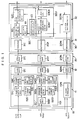
Fig. 1 is a block diagram which shows the schematic
structure of an optical transmitting-receiving system relating to the
first embodiment.
In Fig. 1, the optical transmitting-receiving system relating to
the first embodiment is formed by a transmitting module 10, an
optical fiber array module 20, and a receiving module 30.
The transmitting module 10 is formed by, for example, an
electronic circuit section 11 formed by one LSI and a laser diode (LD)
array section 12.
A clock signal CLK (in the first embodiment, the duty ratio is
50%) and N (N is an integer larger than or equal to 1; e.g., in case of a
parallel transmission of 8 bits or 32 bits, N is equal to 8 or 32)
transmission data Data 1 to DataN are input to the electronic circuit
section 11 of the transmitting module 10. The electronic circuit
section 11 is formed by an LD (Laser Diode, hereinafter it may be
referred to just as LD) current control portion 11C for a clock signal
and LD current control portions 11D1, ..., 11DN for transmission
data Data1, ..., DataN.
The LD
current control portion 11C for a clock signal is
formed by an
inversion amplifying circuit 51C equipped with a
voltage-to-current converting function (hereinafter,
inversion
amplifying circuit
), a bias
current circuit 52C for determining
amplitude (hereinafter,
first bias current circuit
), a laser diode
minimum
current circuit 53C (hereinafter,
second bias current
circuit
), and a current adding
circuit 54C.
The inversion amplifying circuit 51C inverts/amplifies the
clock signal CLK formed by a voltage signal, and at the time of
inversion/amplification, the inversion amplifying circuit 51C
converts the clock signal into a current signal and supplies the
inverted/amplified clock signal (current signal) to the current adding
circuit 54C. The first bias current circuit 52C supplies to the
inversion amplifying circuit 51C a bias current for determining
amplitude (difference in currents between the time in which logical
level is high and the time in which logical level is low) of a driving
current supplied to a laser diode 12C, which will be described later,
so as to obtain a desirable amplitude of the amplified current (the
clock signal). The reason for which the inversion amplifying circuit
51C inverts/amplifies will be described later.
In a case in which transmission loss is large due to a long
transmission distance and the quality of transmission is adversely
affected, a bias current for determining amplitude generated by the
first bias current circuit 52C may be selected so that the difference
between the time in which logical level is high and the time in which
logical level is low is large.
The second bias current circuit 53C outputs the minimum
bias current of the driving current to the laser diode 12C, which will
be described later. In the first embodiment, this bias current is set to
a current larger than the largest threshold value current within the
range of operating temperature of the laser diode 12C.
Fig. 3 is an explanation auxiliary view of the above
description and shows a relationship between the driving current of
the laser diode 12C and an output power characteristic. The light
emission of the laser diode 12C is started from a small driving current
Iℓ at a low temperature Tℓ (e.g., 0 °C), and as the driving current is
increased, the intensity of light emission is increased. On the other
hand, the light emission of the laser diode 12C is started from a
driving current Ih, which is larger than the above-described driving
current Iℓ, at a high temperature Th (e.g., 80 °C), and as the driving
current is increased, the intensity of light emission is increased. If
the operating temperature compensated by the transmission system
is 0 °C to 80 °C, the bias current (IB) from the second bias current
circuit 53C is selected to a current which is larger than the driving
current (the threshold value current), from which the light emission
of the laser diode 12C is started.
The current adding circuit 54C synthesizes (adds) the clock
signal (the current signal) from the inversion amplifying circuit 51C
and the bias current from the second bias current circuit 53C so as to
supply the driving current to the corresponding laser diode 12C.
As described above, the current from the inversion
amplifying circuit 51C is not directly supplied to the laser diode 12C.
Instead, the above-described current and the bias current from the
second bias current circuit 53C are synthesized (added) and supplied
to the laser diode 12C according to the following reason. In a case in
which the current from the inversion amplifying circuit 51C is directly
supplied to the laser diode 12C, the driving current having low logical
level is substantially 0. Thus, an unfavorable influence due to the
pattern effect of the laser diode, which was referred to the
conventional drawbacks, may occur. On the other hand, as
described in the first embodiment, in a case in which the bias current
which is larger than the largest threshold value current within the
range of operating temperature of the laser diode 12C is added, the
laser diode 12C is invariably in an oscillated state, and the adverse
influence due to the pattern effect of the laser diode 12C can be
prevented beforehand.
In a case in which the pattern effect influences greatly the
quality of reception data in relation to the transmission distance or
the quality of transmission, it suffices if the bias current generated by
the second bias current circuit 53C takes a sufficient margin from the
largest threshold value current within the range of operating
temperature of the laser diode 12C.
Fig. 4 is a circuit diagram which shows a concrete circuit
example of the LD current control portion 11C for a clock signal.
The LD current control portion 11C for a clock signal shown
in Fig. 4 is a circuit in which a ground potential G is a high power
supply voltage and which centers around differential amplifying pair
of transistors Q1 and Q2. A common emitter for the differential
amplifying pair of transistors Q1 and Q2 is connected to a constant
current source corresponding to the first bias current circuit 52C.
Further, a corresponding laser diode 12C is serially connected to the
collector of the transistor Q2, and the connecting point
(corresponding to the current adding circuit 54C) between the laser
diode 12C and the collector of the transistor Q2 is connected to a
constant current source corresponding to the second bias current
circuit 53C. Moreover, the clock signal (the voltage signal) CLK is
applied to the base pair of the differential amplifying pair of
transistors Q1 and Q2.
Namely, in the LD current control portion 11C for a clock
signal shown in Fig. 4, as the clock signal (the voltage signal) CLK is
applied to the differential amplifying pair of transistors Q1 and Q2, to
which a constant current is flowed from the constant current source
corresponding to the first bias current circuit 52C, a collector current
whose logic is inverted from the logic of the clock signal CLK, flows to
the collector of the transistor Q2. The collector current and a bias
current generated by the constant current source corresponding to
the second bias current circuit 53C are added by connection and the
added current thereby flows to the laser diode 12C.
On the other hand, as shown in detail in Fig. 1 regarding the
transmission data Data1, the LD current control portion 11DX (X is 1
to N) for each transmission data includes an inversion amplifying
circuit 51DX, a first bias current circuit 52DX, a second bias current
circuit 53DX, a current adding circuit 54DX, as in the same way as
the LD current control portion 11C for a clock signal. In addition, the
LD current control portion 11DX includes a latch circuit 50DX.
Descriptions of functions of the inversion amplifying circuit 51DX,
the first bias current circuit 52DX, the second bias current circuit
53DX, and the current adding circuit 54DX are omitted.
The latch circuit 50DX latches an input transmission data
DataX on the basis of the clock signal CLK and supplies the data to
the inversion amplifying circuit 51DX. In this way, even if the
synchronization of N transmission data; Data1 to Data N, which are
transmitted in parallel and input to the electronic circuit section 11 of
the transmitting module 10, are disordered more or less, the
synchronization of data is made reliable.
It is significant that the inversion amplifying circuit 51DX be
used in the LD current control portion 11DX for a transmission data.
As mentioned above, when the logic of the input
transmission data DataX is
0
, the inversion amplifying circuit 51DX
serves to flow a large driving current to the laser diode 12DX, which
will be described later. In general, if a processing such as scrambler
or the like is not carried out, there are many
0
s in the transmission
data DataX (e.g., in case of an RZ signal, there are many
0
s). In a
case in which the transmission data DataX is not inverted and the
laser diode 12DX is driven, the rate of
0
in the driving pattern is
increased and the unfavorable influence due to the aforementioned
pattern effect of the laser diode 12DX occurs. Thus, in the first
embodiment, the inversion amplifying circuit 51DX is provided, and
when the rate of
0
in the input transmission data DataX is high, a
large driving current is flowed to the laser diode 12DX such that the
unfavorable influence due to the pattern effect is prevented.
In a case in which the rate of
1
in the transmission data
DataX is high, a simple voltage-to-current converting circuit may be
used instead of the inversion amplifying circuit 51DX. Namely, an
inversion amplifying circuit or a non-inversion amplifying circuit may
be selected so as to prevent the pattern effect from occurring to the
laser diode 12DX.
By the way, in an electrical transmitting system, a low
electric power consumption is expected, so that the rate of low driving
voltage is increased in a driving voltage or the like with respect to a
transmitting path. However, as described in the above drawbacks, in
case of an optical transmission, since there is a drawback in that the
quality of transmission from the phase surface is deteriorated, the
inversion amplifying circuit 51DX is provided.
Since the duty ratio of the clock signal CLK is 50%, the
inversion amplifying circuit 51C may be omitted. However, in case of
the first embodiment, as will be described later, it is preferable that
the influence due to the temperature variation or the like is the same
between the transmission of the clock signal CLK and that of the
transmission data DataX. Consequently, the inversion amplifying
circuit 51C is also provided for detecting the transmission processing
of the clock signal CLK.
The concrete circuit structure of the LD current control
portion 11DX (X is 1 to N) for each transmission data is unillustrated.
However, a general concrete structure serving as a D-type flip-flop
circuit (a latch circuit) which is added to the circuit structure shown
in the aforementioned Fig. 4 can be mentioned.
The laser diode array section 12 includes laser diodes 12C,
12D1, ..., 12DN corresponding to the number of clock signal CLK and
transmission signals of respective transmission data Data X. The
laser diodes 12C, 12D1, ..., 12DN are provided closely on, e.g., the
same wafer substrate. The laser diodes 12C, 12D1, ..., 12DN carry
out electrical-to-optical conversions in accordance with the driving
currents from the current adding circuits 54C, 54D1, ..., 54DN, and
the converted optical signals are incident on corresponding optical
fibers 21C, 21D1, ..., 21DN.
The optical fiber array module 20 is formed by the optical
fibers 21C, 21D1, ..., 21DN corresponding to the clock signal CLK
and the number of transmission signals of respective transmission
data DataX. The optical fibers 21C, 21D1, ..., 21DN are disposed in a
row on a tape member. Alternatively, the optical fibers 21C, 21D1, ...,
21DN, which correspond to the clock signal CLK and the number of
transmission signals of respective transmission data DataX, are
disposed in a row in the shape of a concentric circle around a core
wire. The optical fibers 21C, 21D1, ..., 21DN guide the optical signals
from the corresponding laser diodes 12C, 12D1, ..., 12DN to the
corresponding photodiodes 31C, 31D1, ..., 31DN, to be described
later.
The receiving module 30 is formed by a photodiodes (PD)
array section 31 and an electronic circuit section 32, which is formed
by, e.g., an LSI.
The photodiodes array section 31 includes photodiodes 31C,
31D1, ..., 31DN, which correspond to the clock signal CLK and the
number of transmission signals of respective transmission data Data
X. The photodiodes 31C, 31D1, ..., 31DN are disposed closely on,
e.g., the same wafer substrate. The photodiodes array section 31
converts the optical signals from the corresponding optical fibers
21C, 21D1, ..., 21DN and outputs electric signals (including current
signals or voltage signals converted therefrom).
The electronic circuit section 32 is formed by a reception
processing portion 32C for a clock signal and reception processing
portions 32D1, ..., 32DN for respective transmission (received) data.
The reception processing portion 32C for a clock signal
includes an electric signal distributor 60, an integrating circuit 61, a
code identification regenerating circuit 62C, and an identification
level multiplying circuit 63.
The electric signal distributor 60 divides an electric signal
from the photodiodes 31C in two and distributes one of the branch
signals to the integrating circuit 61 and the other of the branch
signals to the code identification regenerating circuit 62C. The levels
of respective branch signals are half the level of the signal before
branched.
The integrating circuit 61 includes a sufficiently large time
constant so as to integrate and convert the input branch signal into a
signal having a DC level. Because the branch signal input to the
integrating circuit 61 has a clock signal component having the duty
ratio of 50%, the converted DC level is the center level of amplitudes
of the input branch signal. The DC level is supplied to the code
identification regenerating circuit 62C as an identification level for
determining a code. Namely, in the first embodiment, since the
identification level is formed by the received signal (the clock signal),
the identification level varies in accordance with the level variations
or the like of the received signal.
The code identification regenerating circuit 62C compares
the size of the level of the branch signal from the electric signal
distributor 60 to that of the identification level from the integrating
circuit 61 so as to regenerate a transmitted clock signal (determine a
code). In the regeneration processing, a high level and a low level in
the input signal is inverted so as to regenerate a clock signal. This
corresponds to the fact that the inversion amplifying circuit 51C is
provided at the transmitter side.
The identification level multiplying circuit (DC amplifying
circuit) 63 multiplies the level of identification level from the
integrating circuit 61 by a predetermined amount and supplies the
multiplied level to the reception processing portions 32D1, ..., 32DN
for all of the transmission (received) data as the identification level for
the circuit.
At the transmitter side, in a case in which the bias currents
in all of the first bias current circuits 52C, 52D1, ..., 52DN are equal
and the bias currents in all of the second bias current circuits 53C,
53D1, ..., 53DN are equal, the number of multiplication is two.
Because the level of the received signal relating to the clock signal is
halved by the branching processing of the electric signal distributor
60, the identification level from the integrating circuit 61 cannot be
used as it is by the reception processing portions 32D1, ..., 32DN for
transmission (received) data. The identification level multiplying
circuit 63 is thereby provided.
In a case in which the bias current in the first bias current
circuit 52C for a clock signal is different from the bias currents in the
first bias current circuits 52D1, ..., 52DN and/or in a case in which
the bias current in the second bias current circuit 53C for a clock
signal is different from the bias currents in the second bias current
circuits 53D1, ..., 53DN for transmission data, the number of
multiplication at the identification level multiplying circuit 63 may be
selected in accordance with the difference in the bias currents.
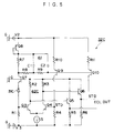
Fig. 5 is a circuit diagram which shows the concrete circuit
example of the reception processing portion 32C for a clock signal.
As shown in Fig. 5, the reception processing portion 32C for a clock
signal operates with a positive power supply V2, a negative power
supply V3, and a ground potential G serving as power supply
voltages.
In Fig. 5, a differential amplifying circuit portion which is
formed by a pair of NPN transistors Q3, Q4 is a circuit portion which
directly determines a code. The NPN transistor Q3 includes a load
resistor R2 and the NPN transistor Q4 includes a load resistor R3,
and the emitters of the NPN transistors Q3, Q4 are connected in
common to a constant current source IS. The differential amplifying
circuit portion formed by the pair of NPN transistors Q3, Q4 operates
with the difference between the ground potential G and the negative
power supply voltage V3 serving as a power supply voltage.
The emitter and the collector of a PNP transistor Q8 whose
base and collector are connected to the high voltage side of the
integrating circuit 61, a resistor R7, the emitter and the collector of
an NPN transistor Q7 whose base is set to the ground potential G, a
photodiodes 31C, and a resistor R1 are connected serially between
the positive power supply voltage V2 and the negative power supply
voltage V3. The connecting point between the anode of the photodiodes
31C and the resistor R1 is connected to the base of the
transistor Q3. In accordance with the intensity of received light, the
current flowed to the photodiodes 31C is converted into a voltage by
the resistor R1 and the converted voltage is applied to the base of the
transistor Q3.
Further, a resistor R10, the emitter and the collector of a PNP
transistor Q9 whose base is connected to the low voltage side of the
integrating circuit 61, and a resistor R4 are connected serially
between the positive power supply voltage V2 and the negative power
supply voltage V3. The connecting point between the collector of the
transistor Q9 and the resistor R4 is connected to the base of the
transistor Q4. In accordance with the charge voltage of the
integrating circuit 61, the current (although variable, a constant
current in a short period) flowed to the serial circuit is converted into
a voltage by the resistor R4, and the converted voltage is applied to
the base of the transistor Q4.
When the intensity of light to the photodiodes 31C is large
and a large current flows to the photodiodes 31C, the voltage applied
to the base of the transistor Q3 is larger than the voltage applied to
the base of the transistor Q4, and the collector voltage of the
transistor Q3 is smaller than the collector voltage of the transistor
Q4. On the other hand, when the intensity of light to the photodiodes
31C is small and a small current flows to the photodiodes
31C, the voltage applied to the base of the transistor Q3 is smaller
than the voltage applied to the base of the transistor Q4, and the
collector voltage of the transistor Q3 is larger than the collector
voltage of the transistor Q4.
Between the ground potential G and the negative power
supply voltage V3, an output circuit is structured by a serial circuit
(emitter-follower circuit) formed by an NPN transistor Q5 whose base
is connected to the collector of the transistor Q3 and a resistor R5
and a serial circuit formed by an NPN transistor Q6 whose base is
connected to the collector of the transistor Q4 and a resistor R6. A
voltage difference between the collector voltages of the transistors Q3
and Q4 is output without being inverted and amplified.
The circuit portion, in which a resistor R8, a capacitor C1, a
resistor R9, and a capacitor C2 are connected in a ladder shape,
forms the integrating circuit 61. One end of the resistor R8 is
connected to the connecting point (corresponding to the electric
signal distributor 60) between the aforementioned resistor R7 and
the collector of the transistor Q7. Further, the common connecting
point between the capacitors C1 and C2 are connected to the
connecting point between the resistor R7 and the collector (and the
base) of the transistor Q8. Consequently, in accordance with the
voltage generated at the ends of the resistor R7 based on the current
flowed to the photodiodes 31C, the integrating circuit 61 is charged or
discharged. The time constant of the integrating circuit 61
determined by the capacities of the capacitors C1 and C2 is large, the
charge voltage of the integrating circuit 61 is stable for the most part.
The charge voltage of the integrating circuit 61 is applied to
the base of the aforementioned transistor Q9, and the transistor Q9
and the resistor R10 form a current source. A current generated by
the current source is converted into a voltage by the resistor R4, and
as mentioned above, the converted voltage is applied to the base of
the transistor Q4 as a reverence voltage for determining a code.
A resistor R11 and a PNP transistor Q10, which are
connected serially at the positive power supply voltage V2 side, form
a current source circuit and correspond to the level multiplying
circuit 63. The charge voltage of the integrating circuit 61 is applied
to the base of the transistor Q10. Due to the relationship between the
resistance value (r) of the resistor R11 and the resistance value (2r) of
the resistor R10, a current which is twice as large as that of the
transistor Q9 flows to the transistor Q10.
Although unillustrated, the collector of the transistor Q10 is
connected to the circuit portion, which corresponds to the transistor
Q4 and the resistor R4, of a reception processing portion 32DX for
any of the transmission (received) data, to be described later. Fig. 5
shows only one serial circuit of the resistor R11 and the transistor
Q10. However, serial circuits which correspond to the number of
reception processing portions 32D1 to 32DN for transmission
(received) data may be provided.
The reception processing portion 32DX (X is 1 to N) for each
transmission (received) data includes a code identification
regenerating circuit 62DX and a latch circuit 64DX.
The code identification regenerating circuit 62DX compares
the size of the level of the electric signal from the corresponding
photodiodes 32DX to the size of the identification level from the level
multiplying circuit 63 so as to regenerate a transmitted transmission
data DataX (determine a code). In this regeneration processing as
well, the high level and the low level of the input signal is inverted so
as to regenerate a transmission DataX.
The latch circuit 64DX delivers the regenerated transmission
data DataX to a device in the next stage on the basis of the
regenerated clock signal CLK.
Figs. 6A through 6E and Figs. 7A through 7E are timing
charts of respective portions in an optical transmitting-receiving
system of the first embodiment.
At the transmitter side, the input clock signal (the voltage
signal) CLK shown in Fig. 6A is inverted/amplified and is made a
voltage-to-current conversion at the inversion amplifying circuit 51C.
As shown in Fig. 6B, the input clock signal CLK is converted into a
signal which has an amplitude determined by the bias current from
the first bias current circuit 52C and whose logical level is inverted.
The signal is then supplied to the current adding circuit 54C. At the
current adding circuit 54C, a bias current from the second bias
current circuit 53C is added to the signal. The added signal is
converted into a driving signal having a DC offset shown in Fig. 6C.
The driving signal is supplied to the laser diode 12C so as to be made
an electrical-to-optical conversion and is incident on the optical fiber
21C.
Further, at the transmitter side, the input transmission data
(the voltage signal) Data1 is latched at the latch circuit 50D1 on the
basis of the clock signal CLK. Data1 is converted into a data
synchronized with the clock signal shown in Fig. 7A, and thereafter,
the data is inverted/amplified and is made an voltage-to-current
conversion at the inversion/ amplifying circuit 51D1. As shown in
Fig. 7B, the input transmission data Data1 is converted into a signal
which has an amplitude determined by the bias current from the first
bias current circuit 51D1 and whose logical level is inverted. The
converted signal is then supplied to the current adding circuit 54D1.
At the current adding circuit 54D1, the bias current from the second
bias current circuit 53D1 is added to the signal. The added signal is
converted into a driving signal having a DC offset shown in Fig. 7C.
The driving signal is supplied to the laser diode 12D1 so as to be
made an electrical-to-optical conversion and is incident on the optical
fiber 21D1.
The same processing is effected on the other transmission
data Data2 to DataN, and the signals are incident on the optical
fibers 21D2 to 21DN from the laser diodes 12D2 to 12DN.
On the other hand, at the receiver side, the received signal
which was made an optical-to-electrical conversion by the photodiodes
31C for a clock signal is divided in two at the electric signal
distributor 60. The branched signal shown in Fig. 6D is supplied to
the integrating circuit 61 and the code identification regenerating
circuit 62C. In Fig. 6D, the branched signal is illustrated in the shape
of square waves, however, an actual branched signal is more
sinusoidal than the illustrated signal. At the integrating circuit 61, as
the branched signal is integrated, the identification level L1 shown in
Fig. 6D is formed so as to be supplied to the code identification
regenerating circuit 62C. The code identification regenerating circuit
62C compares the size of the identification level to that of the
branched signal (including inversion processing) so as to regenerate
the transmitted clock signal shown in Fig. 6E.
The identification level from the integrating circuit 61 is
multiplied by a predetermined amount (e.g., 2) by the identification
level multiplying circuit 63, converted into an identification level (e.g.,
2 × L1) for the regeneration of transmission data shown in Fig. 7D,
and supplied to the reception processing portions 32D1 to 32DN for
all of the transmission (received) data.
The received signal, which is made an optical-to-electrical
conversion by the photodiodes 31D1 for transmission data and
shown in Fig. 7D, is supplied to the code identification regenerating
circuit 62D1. In Fig. 7D, the received signal is illustrated in the
shape of square waves, however, the actual received signal is more
sinusoidal than the illustrated signal. The code identification
regenerating circuit 62D1 compares the size of the identification level
from the identification level multiplying circuit 63 to that of the
received signal (including inversion processing). As shown in Fig.
7E, the transmission data Data1 is regenerated. The regenerated
transmission data1 is latched at the latch circuit 64D1 on the basis of
the regenerated clock signal CLK and is delivered to a device in the
next stage.
In accordance with the optical transmitting apparatus, the
optical receiving apparatus, and the optical transmitting-receiving
system in the aforementioned first embodiment, the following effects
can be achieved.
Second Embodiment
A second embodiment in which an optical transmitting
apparatus, an optical receiving apparatus, and an optical
transmitting-receiving system are applied to a system which employs
an optical interconnecting method will be described in detail with
reference to the drawings.
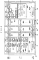
Fig. 8 is a block diagram which shows the schematic
structure of an optical transmitting-receiving system of the second
embodiment. The portions which are the same as and which
correspond to those in Fig. 1 relating to the aforementioned first
embodiment are denoted by the same reference numerals.
As is clearly seen from the comparisons between Fig. 8 and
Fig. 1, in the second embodiment, in addition to the structure of the
first embodiment, a frequency dividing circuit 55 is provided within
an LD current control portion 11C for a clock signal, and a frequency
multiplying circuit 65 is provided within a reception processing
portion 32C for a clock signal.
The frequency dividing circuit 55 divides the frequency of an
input clock signal CLK in two and supplies the divided frequency to
an inversion amplifying circuit 51C. The frequency multiplying
circuit 65 multiplies the frequency of the signal from a code
identification regenerating circuit 62C by two so that a clock signal is
regenerated at last. The functions of other structural elements are
the same as those of the first embodiment, and descriptions thereof
are omitted.
The basic frequency component of the clock signal CLK is
higher than the basic frequency component of the transmission data
DataX (see Figs. 6 and 7). Due to the frequency characteristics of the
optical fiber, the difference in these frequency components may
slightly change the degree of level changes between the received
signal relating to the clock signal and the received signal relating to
the transmission data. Accordingly, the frequency dividing circuit 55
and the frequency multiplying circuit 65 are provided in the second
embodiment, such that the frequency components of optical signals
transmitted within all of the optical fibers are made as uniform as
possible.
The effects of the second embodiment are similar to those of
the aforementioned first embodiment. Additionally, since the
frequency components of optical signals can be made as uniform as
possible, the transmission precision at a phase surface can be
further improved.
Third Embodiment
Next, a third embodiment, in which an optical transmitting
apparatus, an optical receiving apparatus, and an optical
transmitting-receiving system are applied to a system which employs
an optical interconnecting method, will be described in detail with
reference to the drawings.
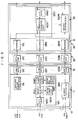
Fig. 9 is a block diagram which shows the schematic
structure of the optical transmitting-receiving system relating to the
third embodiment. The portions which are the same as or correspond
to those in Fig. 1 relating to the aforementioned first embodiment are
denoted by the same reference numerals.
In the third embodiment, an identification level bias current
circuit 56 is provided. The identification level bias current circuit 56
supplies a bias current (a driving current), which corresponds to the
identification level used for determining the code of a transmission
data at the receiver side, and to a laser diode 12C so as to emit a light.
The optical signal is made an optical-to-electrical conversion into an
electric signal (an identification level) by a photodiodes 31C, and the
electric signal is supplied to reception processing portions 32D1 to
32DN for all of the transmission data. Namely, the identification level
is transmitted directly and not transmitted by using a clock signal.
Even in the third embodiment, since the information about
the identification level is transmitted from the transmitter side to the
receiver side, the identification level also varies in accordance with
the temperature variations or the like. The third embodiment can
achieve an effect, which is caused by using a variable identification
level and which was referred to the description of the effect in the first
embodiment, as it is.
The influence due to the temperature variations or the like in
the electric circuit portion is different between in the transmitting
route of the identification level and in that of the transmission data.
However, the influence due to the temperature variations or the like
is much larger in the optical signal processing system than in the
electric signal processing system. The effect referred to the
description of the effect in the first embodiment can be achieved as it
is.
As is clearly seen from the comparison between Fig. 9 and
Fig. 1, the structure of the third embodiment is very simple.
It is most preferable if the third embodiment is applied to a
transmitting-receiving system including a circuit which generates a
clock component from a received data. Although not shown in Fig. 9,
the clock signal may also be transmitted regardless of the
transmission of the identification level information.
In case of the third embodiment, the photodiodes 31C serves
as identification level supplying means described in claim 4.
Other Embodiments
In the above embodiments, an identification level
information is transmitted by one route. However, the identification
level may be transmitted by a plurality of routes. For example, if a
transmission data includes 32 bits, the identification level
information may be transmitted by a sum of four routes, each per
eight bits. In this case, a set of laser diode for identification level
information and an optical fiber corresponding to this diode may be
provided in the midway among the sets of laser diodes for 8-bit
transmission data and optical fibers corresponding to each of the
laser diodes.
Further, in the above embodiments, the present invention is
applied to a case in which transmission data is conveyed in parallel.
However, the present invention is applicable even to a case in which
there is only one transmission data. In this case as well, the effect of
reducing the jittering of regenerated data is expected. Namely, the
present invention is carried out in consideration of an optical
transmitting-receiving system in accordance with an optical
interconnecting method. However, it goes without saying that the
present invention is applicable to the other optical transmitting-receiving
system.
Moreover, in the above embodiments, there are a technical
idea in which the logical level of a transmission data is adjusted such
that the emission of light increases at the side in which the optical
intensity of laser diode is large, a technical idea in which a current
which is larger than the threshold value current invariably flows to a
laser diode within the range of operating temperature, and a
technical idea in which an identification level is transmitted from the
an optical transmitting apparatus to an optical receiving apparatus
may be applied to an optical transmitting-receiving system. It goes
without saying that these ideas may be applied independently to the
optical transmitting-receiving system.
Furthermore, in the above embodiments, because the logical
level of the transmission data is adjusted so that the emission of light
increases at the side in which the optical intensity of the laser diode is
large, the logical level thereof is inverted fixedly. However, the
inversion or non-inversion of the logical level may be selected by
inputting the rate information from outside as to which logical level
appears more frequently. For example, this can be achieved by; an
inverter circuit which inverts a transmission data, a switch which
selects a transmission data which passes through the inverter circuit
or a transmission data which does not pass through the inverter
circuit in accordance with the rate information, and a circuit which
performs a voltage-to-current conversion of the switch output. In
this case, it requires that a transmitting system which transmits the
rate information to the optical receiving apparatus be provided and
the inversion and non-inversion of the logical level can be selected at
the optical receiving apparatus.
Still further, in the above embodiments, the bias currents are
the same at the transmitting route of the clock signal and at the
transmitting route of the transmission data. However, there is no
doubt that the bias currents may be different.
In accordance with the optical transmitting apparatus of the
first aspect, the optical receiving apparatus of the second aspect, and
the optical transmitting-receiving system of the third aspect, the
identification level information is transmitted between the optical
transmitting apparatus and the optical receiving apparatus. The
identification level at the receiver side includes variations due to the
temperatures or the like similar to those of the transmitted data,
such that the transmission data can be regenerated properly from the
phase surface thereof.
Further, in accordance with the optical transmitting
apparatus of the fourth aspect, the optical receiving apparatus of the
Fifth aspect, and the optical transmitting-receiving system of the sixth
aspect, it is arranged such that the transmission data is transmitted
in such a mode that the logical level of the transmission data whose
rate of appearance is high is the side in which the optical intensity of
the optical signal from the light emitter is large. Consequently, the
rate in which the light emitter of the optical transmitting apparatus
emits light at a strong optical intensity is increased, the average
response in optical emission of the light emitter is improved, and the
unfavorable effect (pattern effect) on the phase surface or the like due
to the delay in response of the light emitter can be reduced.
Moreover, in accordance with the optical transmitting
apparatus of the seventh aspect, even if the logical level of the
transmission data is low, the light emitter applies bias to the
transmission data and emits light so that the logical level is larger
than the lowest level of emission within the range of operating
temperature of the optical transmitting apparatus. Therefore, the
unfavorable effect (pattern effect) on the phase surface or the like due
to the delay in response of the light emitter can be reduced.