EP0851642A2 - Multicarrier receiver with compensation for frequency offset and for frequency-dependent distortion - Google Patents
Multicarrier receiver with compensation for frequency offset and for frequency-dependent distortion Download PDFInfo
- Publication number
- EP0851642A2 EP0851642A2 EP97310598A EP97310598A EP0851642A2 EP 0851642 A2 EP0851642 A2 EP 0851642A2 EP 97310598 A EP97310598 A EP 97310598A EP 97310598 A EP97310598 A EP 97310598A EP 0851642 A2 EP0851642 A2 EP 0851642A2
- Authority
- EP
- European Patent Office
- Prior art keywords
- frequency
- modulated signal
- signal
- variation
- compensating
- Prior art date
- Legal status (The legal status is an assumption and is not a legal conclusion. Google has not performed a legal analysis and makes no representation as to the accuracy of the status listed.)
- Granted
Links
- 230000001419 dependent effect Effects 0.000 title 1
- 230000036962 time dependent Effects 0.000 claims description 23
- 238000000034 method Methods 0.000 claims description 21
- 230000005540 biological transmission Effects 0.000 claims description 19
- 238000009499 grossing Methods 0.000 claims description 9
- 238000010586 diagram Methods 0.000 description 10
- 230000003111 delayed effect Effects 0.000 description 6
- 238000007796 conventional method Methods 0.000 description 3
- 230000001934 delay Effects 0.000 description 3
- 238000005070 sampling Methods 0.000 description 3
- 230000015556 catabolic process Effects 0.000 description 2
- 238000006731 degradation reaction Methods 0.000 description 2
- 230000001360 synchronised effect Effects 0.000 description 2
- 230000010363 phase shift Effects 0.000 description 1
- 230000001902 propagating effect Effects 0.000 description 1
Images

Classifications
-
- H—ELECTRICITY
- H04—ELECTRIC COMMUNICATION TECHNIQUE
- H04L—TRANSMISSION OF DIGITAL INFORMATION, e.g. TELEGRAPHIC COMMUNICATION
- H04L25/00—Baseband systems
- H04L25/02—Details ; arrangements for supplying electrical power along data transmission lines
- H04L25/03—Shaping networks in transmitter or receiver, e.g. adaptive shaping networks
- H04L25/03006—Arrangements for removing intersymbol interference
- H04L25/03159—Arrangements for removing intersymbol interference operating in the frequency domain
-
- H—ELECTRICITY
- H04—ELECTRIC COMMUNICATION TECHNIQUE
- H04L—TRANSMISSION OF DIGITAL INFORMATION, e.g. TELEGRAPHIC COMMUNICATION
- H04L27/00—Modulated-carrier systems
- H04L27/26—Systems using multi-frequency codes
- H04L27/2601—Multicarrier modulation systems
- H04L27/2647—Arrangements specific to the receiver only
- H04L27/2649—Demodulators
- H04L27/2653—Demodulators with direct demodulation of individual subcarriers
-
- H—ELECTRICITY
- H04—ELECTRIC COMMUNICATION TECHNIQUE
- H04L—TRANSMISSION OF DIGITAL INFORMATION, e.g. TELEGRAPHIC COMMUNICATION
- H04L27/00—Modulated-carrier systems
- H04L27/26—Systems using multi-frequency codes
- H04L27/2601—Multicarrier modulation systems
- H04L27/2647—Arrangements specific to the receiver only
- H04L27/2655—Synchronisation arrangements
- H04L27/2657—Carrier synchronisation
-
- H—ELECTRICITY
- H04—ELECTRIC COMMUNICATION TECHNIQUE
- H04L—TRANSMISSION OF DIGITAL INFORMATION, e.g. TELEGRAPHIC COMMUNICATION
- H04L27/00—Modulated-carrier systems
- H04L27/26—Systems using multi-frequency codes
- H04L27/2601—Multicarrier modulation systems
- H04L27/2647—Arrangements specific to the receiver only
- H04L27/2655—Synchronisation arrangements
- H04L27/2662—Symbol synchronisation
-
- H—ELECTRICITY
- H04—ELECTRIC COMMUNICATION TECHNIQUE
- H04L—TRANSMISSION OF DIGITAL INFORMATION, e.g. TELEGRAPHIC COMMUNICATION
- H04L27/00—Modulated-carrier systems
- H04L27/26—Systems using multi-frequency codes
- H04L27/2601—Multicarrier modulation systems
- H04L27/2647—Arrangements specific to the receiver only
- H04L27/2655—Synchronisation arrangements
- H04L27/2668—Details of algorithms
- H04L27/2673—Details of algorithms characterised by synchronisation parameters
- H04L27/2676—Blind, i.e. without using known symbols
-
- H—ELECTRICITY
- H04—ELECTRIC COMMUNICATION TECHNIQUE
- H04L—TRANSMISSION OF DIGITAL INFORMATION, e.g. TELEGRAPHIC COMMUNICATION
- H04L25/00—Baseband systems
- H04L25/02—Details ; arrangements for supplying electrical power along data transmission lines
- H04L25/03—Shaping networks in transmitter or receiver, e.g. adaptive shaping networks
- H04L25/03006—Arrangements for removing intersymbol interference
- H04L2025/0335—Arrangements for removing intersymbol interference characterised by the type of transmission
- H04L2025/03375—Passband transmission
- H04L2025/03414—Multicarrier
-
- H—ELECTRICITY
- H04—ELECTRIC COMMUNICATION TECHNIQUE
- H04L—TRANSMISSION OF DIGITAL INFORMATION, e.g. TELEGRAPHIC COMMUNICATION
- H04L25/00—Baseband systems
- H04L25/02—Details ; arrangements for supplying electrical power along data transmission lines
- H04L25/03—Shaping networks in transmitter or receiver, e.g. adaptive shaping networks
- H04L25/03006—Arrangements for removing intersymbol interference
- H04L2025/03433—Arrangements for removing intersymbol interference characterised by equaliser structure
- H04L2025/03439—Fixed structures
- H04L2025/03522—Frequency domain
Abstract
Description

Claims (6)
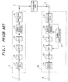
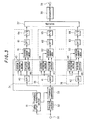
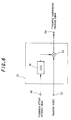
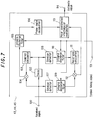
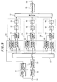
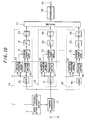
- An apparatus for demodulating a multi-frequency quadrature modulated signal for transmitting data using frequency multiplex transmission using a plurality of frequencies, comprising:a frequency shift estimating means for receiving a multi-frequency quadrature modulated signal and estimating the average frequency shift;a frequency shift compensating means for receiving the frequency shift estimated by the frequency shift estimating means and compensating the frequency shift of the multi-frequency quadrature modulated signal;a band filter set for separating the multi-frequency quadrature modulated signal of which the frequency shift is compensated by the frequency shift compensating means, into different frequency components;a propagation path variation estimating means for estimating the propagation path variation of each of the divided modulated signal components obtained from the band filter set;a propagation path variation compensating means for receiving the propagation path variation estimated by the propagation path variation estimating means and compensating the propagation variation of each of the separated modulated signal components; anda decoding means for receiving the output from the propagation path variation compensating means and decoding the multi-frequency quadrature modulated signal.
- The apparatus according to Claim 1, further comprising:a delaying means for receiving the multi-frequency quadrature modulated signal and delaying the modulated signal;a dividing means for estimating the time-dependent variation in amplitude and phase which has been caused when the modulated signal has passed through the communication path, by dividing the output signal from the delaying circuit by the input signal;a smoothing means for smoothing the output signal from the dividing means; anda compensating means for compensating the time-dependent variation in amplitude and phase of the received signal based on the estimated output signal obtained from the smoothing means.
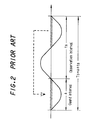
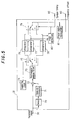
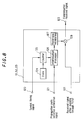
- The apparatus according to Claim 1, further comprising:an interpolating means for receiving the modulated signal and the estimated time-dependent variation of the modulated signal in amplitude and phase and determining the estimate of the time-dependent variation of amplitude and phase in a shorter interval by interpolation; anda compensating means for compensating time-dependent distortion of the modulated signal by dividing the modulated signal by the estimate value determined by the interpolating means.
- A method of demodulating a multi-frequency quadrature modulated signal for transmitting data using frequency multiplex transmission using a plurality of frequencies, comprising:receiving a multi-frequency quadrature modulated signal and estimating the average frequency shift using a frequency shift estimating means;receiving the frequency shift estimated by the frequency shift estimating means and compensating the frequency shift of the multi-frequency quadrature modulated signal using a frequency shift compensating means;separating the multi-frequency quadrature modulated signal of which the frequency shift has been compensated by the frequency shift compensating means, into different frequency components using a band filter;estimating the propagation path variation of each of the divided modulated signal components which have been obtained from the band filter set using a propagation path variation estimating means;receiving the propagation path variation estimated by the propagation path variation estimating means and compensating the propagation variation of each of the separated modulated signal components using a propagation path variation compensating means; andreceiving the output from the propagation path variation compensating means and decoding the multi-frequency quadrature modulated signal using decoding means.
- The method of demodulating a multi-frequency quadrature modulated signal for transmitting data using frequency multiplex transmission using a plurality of frequencies, according to Claim 4, further comprising:receiving the multi-frequency quadrature modulated signal and delaying the modulated signal using a delaying means;estimating the time-dependent variation in amplitude and phase which has been caused when the modulated signal has passed through the communication path, by dividing the output signal from the delaying means by the input signal using a dividing means;smoothing the output signal from the dividing means using a smoothing means; andcompensating the time-dependent variation in amplitude and phase of the received signal based on the estimated output signal obtained from the smoothing means.
- The method of demodulating a multi-frequency quadrature modulated signal for transmitting data using frequency multiplex transmission using a plurality of frequencies according to Claim 4, further comprising:receiving the modulated signal and the estimated time-dependent variation of the modulated signal in amplitude and phase and determining the estimate of the time-dependent variation of amplitude and phase in a shorter interval by interpolation using an interpolating means; andcompensating time-dependent distortion of the modulated signal by dividing the modulated signal by the estimate value determined by the interpolating means.
Applications Claiming Priority (3)
| Application Number | Priority Date | Filing Date | Title |
|---|---|---|---|
| JP34320496 | 1996-12-24 | ||
| JP34320496A JP3431785B2 (en) | 1996-12-24 | 1996-12-24 | Orthogonal frequency multiplex modulation signal demodulator |
| JP343204/96 | 1996-12-24 |
Publications (3)
| Publication Number | Publication Date |
|---|---|
| EP0851642A2 true EP0851642A2 (en) | 1998-07-01 |
| EP0851642A3 EP0851642A3 (en) | 2000-08-23 |
| EP0851642B1 EP0851642B1 (en) | 2006-09-13 |
Family
ID=18359727
Family Applications (1)
| Application Number | Title | Priority Date | Filing Date |
|---|---|---|---|
| EP97310598A Expired - Lifetime EP0851642B1 (en) | 1996-12-24 | 1997-12-24 | Multicarrier receiver with compensation for frequency offset and for frequency-dependent distortion |
Country Status (5)
| Country | Link |
|---|---|
| US (1) | US6058145A (en) |
| EP (1) | EP0851642B1 (en) |
| JP (1) | JP3431785B2 (en) |
| DE (1) | DE69736659T2 (en) |
| ES (1) | ES2270450T3 (en) |
Cited By (5)
| Publication number | Priority date | Publication date | Assignee | Title |
|---|---|---|---|---|
| GB2347285A (en) * | 1999-02-24 | 2000-08-30 | Motorola Ltd | Method and apparatus for frequency synchronisation in a digital radio communications system |
| EP1071227A2 (en) * | 1999-07-21 | 2001-01-24 | NTT DoCoMo, Inc. | CDMA reception apparatus and received signal power measuring apparatus in CDMA mobile communication system |
| GB2366145A (en) * | 2000-07-05 | 2002-02-27 | Fuji Television Network Inc | Underground broadcasting system |
| GB2373973A (en) * | 2001-03-30 | 2002-10-02 | Toshiba Res Europ Ltd | Adaptive OFDM receiver where sets of sub-carriers which are coherent are grouped into sub-bands and a single weight is calculated for each sub-band |
| EP2720426A1 (en) * | 2012-10-09 | 2014-04-16 | Mitsubishi Electric R&D Centre Europe B.V. | Method and a device for correcting a frequency shift on received symbols |
Families Citing this family (18)
| Publication number | Priority date | Publication date | Assignee | Title |
|---|---|---|---|---|
| JP3507683B2 (en) * | 1998-01-09 | 2004-03-15 | 株式会社エヌ・ティ・ティ・ドコモ | Parallel transmission method |
| DE69940235D1 (en) | 1998-05-26 | 2009-02-26 | Panasonic Corp | Modulator, demodulator, and transmission system for OFDM transmission |
| US6177835B1 (en) * | 1998-07-31 | 2001-01-23 | The United States Of America As Represented By The Administrator Of The National Aeronautics And Space Administration | Method and apparatus for high data rate demodulation |
| WO2001001590A1 (en) * | 1999-06-29 | 2001-01-04 | Mitsubishi Denki Kabushiki Kaisha | Automatic frequency control circuit and demodulator |
| JP3676991B2 (en) | 2001-07-05 | 2005-07-27 | 松下電器産業株式会社 | Wireless communication apparatus and wireless communication method |
| US6936377B2 (en) | 2003-05-13 | 2005-08-30 | C. Glen Wensley | Card with embedded IC and electrochemical cell |
| US20040229127A1 (en) | 2003-05-13 | 2004-11-18 | Wensley C. Glen | Polyimide matrix electrolyte |
| US20040253520A1 (en) | 2003-05-13 | 2004-12-16 | Wensley C. Glen | Polyimide matrix electrolyte and improved batteries therefrom |
| US7390336B2 (en) | 2003-07-29 | 2008-06-24 | Solicore, Inc. | Polyimide-based lithium metal battery |
| KR101300453B1 (en) | 2004-07-22 | 2013-08-27 | 솔리코어 인코포레이티드 | Improved battery tab and packaging design |
| KR100707437B1 (en) | 2005-03-03 | 2007-04-13 | 엘지전자 주식회사 | Mobile Communication System Recompensed for the time delay of Receive signal by Multi-Path |
| US20070064740A1 (en) * | 2005-09-19 | 2007-03-22 | Shai Waxman | Device, system and method of clock synchronization |
| JP5278678B2 (en) * | 2006-10-16 | 2013-09-04 | 日本電気株式会社 | Receiving method and receiving apparatus |
| JP4516591B2 (en) * | 2007-11-28 | 2010-08-04 | 日本電信電話株式会社 | Frequency multiplexing signal receiver |
| JP2010045672A (en) * | 2008-08-15 | 2010-02-25 | Nippon Telegr & Teleph Corp <Ntt> | Signal receiver, and signal receiving method |
| JP4940222B2 (en) * | 2008-11-20 | 2012-05-30 | 日本電信電話株式会社 | Signal receiving apparatus and method |
| US8655282B2 (en) * | 2010-10-29 | 2014-02-18 | Qualcomm Incorporated | Multiple signal transformation in wireless receivers |
| CN109859760A (en) * | 2019-02-19 | 2019-06-07 | 成都富王科技有限公司 | Phone robot voice recognition result bearing calibration based on deep learning |
Citations (1)
| Publication number | Priority date | Publication date | Assignee | Title |
|---|---|---|---|---|
| GB2145906A (en) * | 1983-09-01 | 1985-04-03 | Nec Corp | Circuit for establishing accurate sample timing |
Family Cites Families (6)
| Publication number | Priority date | Publication date | Assignee | Title |
|---|---|---|---|---|
| JP3041175B2 (en) * | 1993-11-12 | 2000-05-15 | 株式会社東芝 | OFDM synchronous demodulation circuit |
| JP3074103B2 (en) * | 1993-11-16 | 2000-08-07 | 株式会社東芝 | OFDM synchronous demodulation circuit |
| JP2655108B2 (en) * | 1994-12-12 | 1997-09-17 | 日本電気株式会社 | CDMA transceiver |
| JP3130752B2 (en) * | 1995-02-24 | 2001-01-31 | 株式会社東芝 | OFDM transmission receiving method and transmitting / receiving apparatus |
| US5680421A (en) * | 1995-02-27 | 1997-10-21 | Oki Electric Industry Co., Ltd. | Frame synchronization apparatus |
| DE69634027T2 (en) * | 1995-08-14 | 2005-12-22 | Nippon Telegraph And Telephone Corp. | Acoustic subband echo canceller |
-
1996
- 1996-12-24 JP JP34320496A patent/JP3431785B2/en not_active Expired - Lifetime
-
1997
- 1997-12-11 US US08/988,934 patent/US6058145A/en not_active Expired - Lifetime
- 1997-12-24 ES ES97310598T patent/ES2270450T3/en not_active Expired - Lifetime
- 1997-12-24 DE DE69736659T patent/DE69736659T2/en not_active Expired - Lifetime
- 1997-12-24 EP EP97310598A patent/EP0851642B1/en not_active Expired - Lifetime
Patent Citations (1)
| Publication number | Priority date | Publication date | Assignee | Title |
|---|---|---|---|---|
| GB2145906A (en) * | 1983-09-01 | 1985-04-03 | Nec Corp | Circuit for establishing accurate sample timing |
Non-Patent Citations (4)
| Title |
|---|
| FRENGER, SVENSSON: "A decision directed coherent detector for OFDM" IEEE VEHICULAR TECHNOLOGY CONFERENCE, 28 April 1996 (1996-04-28) - 1 May 1996 (1996-05-01), pages 1584-1588, XP000595798 New York, US * |
| MIGNONE, MORELLO: "CD3-OFDM: a novel demodulation scheme for fixed and mobile receivers" IEEE TRANSACTIONS ON COMMUNICATIONS, vol. 44, no. 9, September 1996 (1996-09), pages 1144-1151, XP000628336 New York, US ISSN: 0090-6778 * |
| MUELLER ET AL.: "Performance of coherent OFDM-CDMA for broadband mobile communications" WIRELESS PERSONAL COMMUNICATIONS, vol. 2, no. 4, 1996, pages 295-305, XP000589619 Amsterdam, NL ISSN: 0929-6212 * |
| SARI ET AL.: "Transmission techniques for digital terrestrial TV broadcasting" IEEE COMMUNICATIONS MAGAZINE, vol. 33, no. 2, February 1995 (1995-02), pages 100-109, XP000505677 Piscataway, US * |
Cited By (16)
| Publication number | Priority date | Publication date | Assignee | Title |
|---|---|---|---|---|
| GB2347285B (en) * | 1999-02-24 | 2001-03-21 | Motorola Ltd | Method and apparatus for frequency synchronisation in a digital radio communications system |
| GB2347285A (en) * | 1999-02-24 | 2000-08-30 | Motorola Ltd | Method and apparatus for frequency synchronisation in a digital radio communications system |
| US7649859B2 (en) | 1999-07-21 | 2010-01-19 | Ntt Docomo, Inc. | Channel identifier assigning method and mobile communications system |
| EP1460777A2 (en) * | 1999-07-21 | 2004-09-22 | NTT DoCoMo, Inc. | CDMA reception apparatus and received signal power measuring apparatus in CDMA mobile communication system |
| EP1071227A2 (en) * | 1999-07-21 | 2001-01-24 | NTT DoCoMo, Inc. | CDMA reception apparatus and received signal power measuring apparatus in CDMA mobile communication system |
| US6999427B1 (en) | 1999-07-21 | 2006-02-14 | Ntt Docomo, Inc. | CDMA reception apparatus and received signal power measuring apparatus in CDMA mobile communication system |
| EP1071227A3 (en) * | 1999-07-21 | 2003-02-19 | NTT DoCoMo, Inc. | CDMA reception apparatus and received signal power measuring apparatus in CDMA mobile communication system |
| EP1460777A3 (en) * | 1999-07-21 | 2005-03-30 | NTT DoCoMo, Inc. | CDMA reception apparatus and received signal power measuring apparatus in CDMA mobile communication system |
| SG101425A1 (en) * | 1999-07-21 | 2004-01-30 | Ntt Docomo Inc | Cdma reception apparatus and received signal power measuring apparatus in cdma mobile communication system |
| GB2366145A (en) * | 2000-07-05 | 2002-02-27 | Fuji Television Network Inc | Underground broadcasting system |
| GB2366145B (en) * | 2000-07-05 | 2002-10-30 | Fuji Television Network Inc | Underground broadcasting system |
| GB2373973B (en) * | 2001-03-30 | 2003-06-11 | Toshiba Res Europ Ltd | Adaptive antenna |
| GB2373973A (en) * | 2001-03-30 | 2002-10-02 | Toshiba Res Europ Ltd | Adaptive OFDM receiver where sets of sub-carriers which are coherent are grouped into sub-bands and a single weight is calculated for each sub-band |
| EP2720426A1 (en) * | 2012-10-09 | 2014-04-16 | Mitsubishi Electric R&D Centre Europe B.V. | Method and a device for correcting a frequency shift on received symbols |
| WO2014057742A1 (en) * | 2012-10-09 | 2014-04-17 | Mitsubishi Electric Corporation | Method, device and computer program for correcting a frequency shift on symbols received by a receiver |
| US9735997B2 (en) | 2012-10-09 | 2017-08-15 | Mitsubishi Electric Corporation | Method, device and computer program for correcting a frequency shift on symbols received by a receiver |
Also Published As
| Publication number | Publication date |
|---|---|
| DE69736659T2 (en) | 2007-09-13 |
| US6058145A (en) | 2000-05-02 |
| DE69736659D1 (en) | 2006-10-26 |
| EP0851642A3 (en) | 2000-08-23 |
| ES2270450T3 (en) | 2007-04-01 |
| EP0851642B1 (en) | 2006-09-13 |
| JPH10190609A (en) | 1998-07-21 |
| JP3431785B2 (en) | 2003-07-28 |
Similar Documents
| Publication | Publication Date | Title |
|---|---|---|
| US6058145A (en) | Method of demodulating a multi-frequency quadrature modulated signal | |
| EP0839423B1 (en) | Pulse shaping for multicarrier modulation | |
| RU2454808C2 (en) | Modulation circuit on several carriers and also transmitting device and receiving device using this circuit | |
| EP0929172B1 (en) | Multicarrier modulation system, with variable symbol rates | |
| US7009931B2 (en) | Synchronization in a multiple-input/multiple-output (MIMO) orthogonal frequency division multiplexing (OFDM) system for wireless applications | |
| KR100581780B1 (en) | Orthogonal frequency-division multiplex transmission system, and its transmitter and receiver | |
| EP0683576B1 (en) | An OFDM digital broadcasting system, and a transmission system and a receiving system used for digital broadcasting | |
| EP0955754B1 (en) | Method and apparatus for achieving and maintaining symbol synchronization in an OFDM transmission system | |
| USRE43305E1 (en) | Transmission system for OFDM-signals with optimized synchronization | |
| US5802117A (en) | Method and apparatus for joint frequency offset and timing estimation of a multicarrier modulation system | |
| EP1108295B1 (en) | Method for forming a training sequeence | |
| US9596118B2 (en) | FBMC receiver using a method for synchronization in a frequency domain | |
| Hazy et al. | Synchronization of OFDM systems over frequency selective fading channels | |
| US6363131B1 (en) | Method and apparatus for joint timing synchronization and frequency offset estimation | |
| EP1039713A2 (en) | Reduction of delay in multicarrier receivers | |
| KR100213100B1 (en) | Frequency error corrector for orthogonal frequency division multiplexing and method therefor | |
| JP3609937B2 (en) | Receiving machine | |
| JP2000022660A (en) | Digital communication equipment | |
| JP2003152673A (en) | Orthogonal frequency multiplex modulated signal demodulating method | |
| JP2004201338A (en) | Transmitter and transmission method | |
| JP3514965B2 (en) | Receiver | |
| KR100226700B1 (en) | Circuit for detecting synchronization in ofdm receiving system | |
| USRE43829E1 (en) | Transmission system for OFDM-signals with optimized synchronization |
Legal Events
| Date | Code | Title | Description |
|---|---|---|---|
| PUAI | Public reference made under article 153(3) epc to a published international application that has entered the european phase |
Free format text: ORIGINAL CODE: 0009012 |
|
| AK | Designated contracting states |
Kind code of ref document: A2 Designated state(s): DE ES FR GB IT |
|
| AX | Request for extension of the european patent |
Free format text: AL;LT;LV;MK;RO;SI |
|
| PUAL | Search report despatched |
Free format text: ORIGINAL CODE: 0009013 |
|
| AK | Designated contracting states |
Kind code of ref document: A3 Designated state(s): AT BE CH DE DK ES FI FR GB GR IE IT LI LU MC NL PT SE |
|
| AX | Request for extension of the european patent |
Free format text: AL;LT;LV;MK;RO;SI |
|
| RIC1 | Information provided on ipc code assigned before grant |
Free format text: 7H 04L 27/26 A, 7H 04L 25/03 B |
|
| RIN1 | Information on inventor provided before grant (corrected) |
Inventor name: KAWABE, TAKESHI Inventor name: OKADA, MINORU Inventor name: KOMAKI, SHOZO |
|
| 17P | Request for examination filed |
Effective date: 20001107 |
|
| AKX | Designation fees paid |
Free format text: DE ES FR GB IT |
|
| 17Q | First examination report despatched |
Effective date: 20040310 |
|
| GRAP | Despatch of communication of intention to grant a patent |
Free format text: ORIGINAL CODE: EPIDOSNIGR1 |
|
| GRAS | Grant fee paid |
Free format text: ORIGINAL CODE: EPIDOSNIGR3 |
|
| GRAA | (expected) grant |
Free format text: ORIGINAL CODE: 0009210 |
|
| AK | Designated contracting states |
Kind code of ref document: B1 Designated state(s): DE ES FR GB IT |
|
| REG | Reference to a national code |
Ref country code: GB Ref legal event code: FG4D |
|
| REF | Corresponds to: |
Ref document number: 69736659 Country of ref document: DE Date of ref document: 20061026 Kind code of ref document: P |
|
| REG | Reference to a national code |
Ref country code: ES Ref legal event code: FG2A Ref document number: 2270450 Country of ref document: ES Kind code of ref document: T3 |
|
| ET | Fr: translation filed | ||
| PLBE | No opposition filed within time limit |
Free format text: ORIGINAL CODE: 0009261 |
|
| STAA | Information on the status of an ep patent application or granted ep patent |
Free format text: STATUS: NO OPPOSITION FILED WITHIN TIME LIMIT |
|
| 26N | No opposition filed |
Effective date: 20070614 |
|
| REG | Reference to a national code |
Ref country code: FR Ref legal event code: PLFP Year of fee payment: 19 |
|
| PGFP | Annual fee paid to national office [announced via postgrant information from national office to epo] |
Ref country code: DE Payment date: 20151211 Year of fee payment: 19 Ref country code: GB Payment date: 20151221 Year of fee payment: 19 |
|
| PGFP | Annual fee paid to national office [announced via postgrant information from national office to epo] |
Ref country code: ES Payment date: 20151214 Year of fee payment: 19 Ref country code: FR Payment date: 20151221 Year of fee payment: 19 |
|
| PGFP | Annual fee paid to national office [announced via postgrant information from national office to epo] |
Ref country code: IT Payment date: 20151228 Year of fee payment: 19 |
|
| REG | Reference to a national code |
Ref country code: DE Ref legal event code: R119 Ref document number: 69736659 Country of ref document: DE |
|
| GBPC | Gb: european patent ceased through non-payment of renewal fee |
Effective date: 20161224 |
|
| REG | Reference to a national code |
Ref country code: FR Ref legal event code: ST Effective date: 20170831 |
|
| PG25 | Lapsed in a contracting state [announced via postgrant information from national office to epo] |
Ref country code: IT Free format text: LAPSE BECAUSE OF NON-PAYMENT OF DUE FEES Effective date: 20161224 Ref country code: FR Free format text: LAPSE BECAUSE OF NON-PAYMENT OF DUE FEES Effective date: 20170102 |
|
| PG25 | Lapsed in a contracting state [announced via postgrant information from national office to epo] |
Ref country code: GB Free format text: LAPSE BECAUSE OF NON-PAYMENT OF DUE FEES Effective date: 20161224 Ref country code: DE Free format text: LAPSE BECAUSE OF NON-PAYMENT OF DUE FEES Effective date: 20170701 |
|
| REG | Reference to a national code |
Ref country code: ES Ref legal event code: FD2A Effective date: 20180507 |
|
| PG25 | Lapsed in a contracting state [announced via postgrant information from national office to epo] |
Ref country code: ES Free format text: LAPSE BECAUSE OF FAILURE TO SUBMIT A TRANSLATION OF THE DESCRIPTION OR TO PAY THE FEE WITHIN THE PRESCRIBED TIME-LIMIT Effective date: 20060913 |
|
| PG25 | Lapsed in a contracting state [announced via postgrant information from national office to epo] |
Ref country code: ES Free format text: LAPSE BECAUSE OF FAILURE TO SUBMIT A TRANSLATION OF THE DESCRIPTION OR TO PAY THE FEE WITHIN THE PRESCRIBED TIME-LIMIT Effective date: 20161225 |