EP0823812B1 - Horizontale S-Form-Korrektionsschaltung - Google Patents
Horizontale S-Form-Korrektionsschaltung Download PDFInfo
- Publication number
- EP0823812B1 EP0823812B1 EP97305691A EP97305691A EP0823812B1 EP 0823812 B1 EP0823812 B1 EP 0823812B1 EP 97305691 A EP97305691 A EP 97305691A EP 97305691 A EP97305691 A EP 97305691A EP 0823812 B1 EP0823812 B1 EP 0823812B1
- Authority
- EP
- European Patent Office
- Prior art keywords
- horizontal
- circuit
- shape
- voltage
- period
- Prior art date
- Legal status (The legal status is an assumption and is not a legal conclusion. Google has not performed a legal analysis and makes no representation as to the accuracy of the status listed.)
- Expired - Lifetime
Links
Images


Classifications
-
- H—ELECTRICITY
- H04—ELECTRIC COMMUNICATION TECHNIQUE
- H04N—PICTORIAL COMMUNICATION, e.g. TELEVISION
- H04N3/00—Scanning details of television systems; Combination thereof with generation of supply voltages
- H04N3/10—Scanning details of television systems; Combination thereof with generation of supply voltages by means not exclusively optical-mechanical
- H04N3/16—Scanning details of television systems; Combination thereof with generation of supply voltages by means not exclusively optical-mechanical by deflecting electron beam in cathode-ray tube, e.g. scanning corrections
- H04N3/27—Circuits special to multi-standard receivers
-
- H—ELECTRICITY
- H04—ELECTRIC COMMUNICATION TECHNIQUE
- H04N—PICTORIAL COMMUNICATION, e.g. TELEVISION
- H04N3/00—Scanning details of television systems; Combination thereof with generation of supply voltages
- H04N3/10—Scanning details of television systems; Combination thereof with generation of supply voltages by means not exclusively optical-mechanical
- H04N3/16—Scanning details of television systems; Combination thereof with generation of supply voltages by means not exclusively optical-mechanical by deflecting electron beam in cathode-ray tube, e.g. scanning corrections
- H04N3/22—Circuits for controlling dimensions, shape or centering of picture on screen
- H04N3/23—Distortion correction, e.g. for pincushion distortion correction, S-correction
- H04N3/233—Distortion correction, e.g. for pincushion distortion correction, S-correction using active elements
Definitions
- the present invention relates to a horizontal S-shape correction circuit suitable for a display unit using an image receiving tube, and more specifically to a technique for reducing M-shape distortion such that the horizontal linearity is reduced at the central portion of an image during a wide angle deflection, and further, when a plurality of sorts of horizontal deflection periods are used, for correcting the other image distortions such as S-shape distortion of an optimum horizontal linearity, inner pin cushion distortion, etc. for each horizontal deflection period.
- the present invention relates to a horizontal S-shape correction circuit suitably used for a display unit so designed as to be operative at various horizontal deflection frequencies.
- the horizontal S-shape correction circuit according to the present invention can automatically set an optimum horizontal deflection frequency so that the S-shape distortion correction of the horizontal linearity can be optimized for each of a plurality of the horizontal deflection frequencies.
- the horizontal linearity distortion has a tendency of M-shape distortion such that the distortion is reduced at the central portion of the image receiving surface, as shown by solid lines in Fig. 1.
- This tendency is prominent in particular in the wide image receiving tube with an aspect ratio (vertical and horizontal ratio) of 9:16, so that there exists a need of improving this problem.
- Fig. 2 shows an example of the improved circuits, which is composed of a horizontal deflecting coil 1, an S-shape correcting capacitor 2, and a secondary resonance circuit 3 for correcting the M-shape distortion.
- the secondary resonance circuit 3 since the secondary resonance circuit 3 is not used, an electron beam of the image receiving tube is deflected right and left, when a saw tooth horizontal deflection current flows through a series circuit composed of the horizontal deflecting coil 1 and the S-shape correcting capacitor 2.
- the linearity thereof can be corrected by changing the beam extension toward the right and left relative to the central portion of the image receiving surface, that is, by adjusting the capacitance value of the S-shape correcting capacitor 2.
- the secondary resonance circuit 3 is added to correct the M-shape distortion.
- the secondary resonance circuit 3 is composed of a coupling capacitor 4, a resonance capacitor 5, and a resonance coil 6, which can resonate at a frequency twice higher than that of the horizontal deflection frequency.
- the voltage across the S-shape correcting capacitor 2 changes from a parabolic waveform (obtained when the secondary resonance circuit is not connected) as shown by a solid line in Fig. 3 to a waveform (obtained when the secondary resonance waveform is superposed upon the parabolic waveform) as shown by a dashed line in Fig. 3, with the result that the M-shape distortion as shown by the solid line shown in Fig. 1 can be corrected.
- the display unit when used as a display terminal of a computer, various horizontal deflection frequencies are usually needed according to the set resolution of the computer signals.
- Fig. 4 shows a related art example of correcting the S-shape distortion used for the display terminal of a computer.
- an auxiliary capacitor group composed of capacitors 7-1, 7-2 and 7-3 is added to the S-shape correcting capacitor 7. Further, each end of each capacitor of the auxiliary capacitor group is grounded through each of three electronic switches 8-1, 8-2 and 8-3, respectively. Further, these electronic switches are controllably turned on or off, respectively in response to three control signals applied externally.
- the image receiving tube having a wide angle deflection and a flat image receiving surface involves a problem related to inner pin cushion distortion as shown in Fig. 5.
- This distortion implies such a phenomenon that even if the side pin cushion is corrected so that the vertical lines are straight on both right and left ends on the screen, since the pin cushion remains at the intermediate portion thereof, the vertical lines are curved inward at the central portion of the screen surface.
- Fig. 6 shows a related art horizontal deflection output circuit for switching the S-shape correction capacitance value, in which a deflecting coil current Iy is passed through a horizontal deflecting coil 1 according to a driving pulse Vd synchronized with the horizontal deflection frequency of an input signal (applied from a front stage (not shown)).
- the reference numeral 7 denotes an S-shape correcting capacitor.
- the following auxiliary S-shape capacitor group 7-1, 7-2 and 7-3 are all not necessary, so that only the S-shape correcting capacitor 7 is used alone.
- auxiliary S-shape correcting capacitors 7-1, 7-2 and 7-3 auxiliary S-shape correction capacitor group connected in parallel to the main S-shape correcting capacitor 3 are added.
- each end of each auxiliary S-shape correcting capacitor is grounded via each of electronic switches 8-1, 8-2 and 8-3. Further, these electronic switches are controllably turned on or off on the basis of a plurality of external control signals Vsw.
- Vsw external control signals
- these electronic switches are controllably turned on or off on the basis of the external control signals Vsw.
- These control signals Vsw are so set that the most appropriate electronic switch circuits can be turned on according to the sort of the input signal (according to the sort of the horizontal deflection frequency of the input signal applied to the display unit).
- EP 0 146 345 discloses an S-correction circuit for a video display apparatus which provides switchable amounts of correction in a given line deflection interval in order to satisfy the requirements of cathode ray tubes having large deflection angles or complex curvature faceplates.
- a second S-shaping capacitor is coupled in parallel with the main S-shaping capacitor by action of a switching transistor. The time at which the transistor is switched may be controlled, for example, by modulating the switching point at a vertical rate, in order to increase the flexibility of the correction circuit.
- the second object of the present invention is to provide a horizontal S-shape correction circuit, which can execute the optimum S-shape correction automatically according to each of various horizontal deflecting frequencies, in spite of a simple circuit construction.
- the present invention provides a horizontal S-shape correction circuit, comprising:
- the reference voltage is changed according to a horizontal deflection frequency.
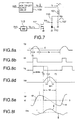
- a horizontal deflecting coil 101 is the same as the deflecting coil 1 of the prior art circuit shown in Fig. 2.
- a horizontal deflection output circuit 109 applies a horizontal output pulse Vp to one end of the horizontal deflecting coil 101, so that a saw tooth current Iy flows through the horizontal deflecting coil 101. Further, this horizontal deflection output circuit 109 executes the well-known horizontal deflection output operation on the basis of a driving pulse Vd applied from a front stage (not shown) of the same circuit 109.
- An S-shape correcting capacitor group connected to the other end of the horizontal deflection coil 101 is composed of a main capacitor 107 grounded directly, and an auxiliary capacitor 110 turned on or off by an electronic switch element 111 connected to the ground.
- the electronic switch 111 is not fixedly turned on or off when the handled frequency is decided, but repeatedly turned on or off in one horizontal deflection period.
- the electronic circuit is composed of an electronic switch element (i.e., FET) 111 and a diode 112 connected in parallel to and between a drain and a source of the switch element 111.
- FET electronic switch element
- diode 112 is connected to flow current in a direction opposite to that of the FET 111, when a sufficient current can flow between the drain and the source of the FET 111 in the reverse direction, it is possible to eliminate this diode 112.
- a mono-stable multivibrator (referred to as MM, hereinafter simply) 113 is triggered by a pulse Vh having the horizontal deflection period.
- a square pulse Vg outputted by this MM 113 is applied to a gate of the FET 111.
- the square pulse Vg outputted by the MM 113 is an external control signal for controlling the turn-on and -off operation of the FET 111.
- the horizontal deflection period pulse Vh is formed in such a way that a constant phase relationship can be kept with respect to the horizontal output pulse (horizontal blanking pulse) Vp, which can be formed easily by waveform shaping the driving pulse Vd or the horizontal output pulse Vp.
- Figs. 8a to 8f are waveform diagrams for assistance in explaining the operation of the circuit shown in Fig. 7.
- Fig. 8b shows the trigger pulse Vh applied to the MM 113.
- this trigger pulse Vh is a square pulse having a pulse width corresponding to the duration in which the horizontal output pulse Vp exceeds a constant level E.
- a circuit for forming this pulse Vh is not shown, this circuit can be obtained easily by use of a comparator for comparing the horizontal output pulse Vp (or a pulse whose voltage is changed to an appropriate level) with a dc voltage E.
- the rise point of the square pulse Vh is determined as time T1. Therefore, the MM 113 is triggered at this time point T1 to generate the square pulse Vg as shown in Fig. 8c.
- the pulse period tmm of the output square pulse Vg of the MM 113 can be changed by moving the operating conditions of the MM 113, so that a fall time point T2 of the square pulse Vg can be adjusted freely.
- the current Idr flowing through the FET 111 and the current Id flowing through the diode 112 become as shown in Fig. 8e.
- the current Idr is of saw tooth waveform in the same way as with the horizontal deflecting coil current Iy, as shown by a dashed line in Fig. 8e.
- the actual current waveform becomes as shown by a solid line in Fig. 8e.
- the positive portion of the current waveform is the drain current Idr of the FET 111, and the negative portion thereof is the current Id of the diode 112.
- the voltage Vcs as shown in Fig. 8f can be developed at the main S-shape correcting capacitor 107.
- the waveform of the voltage Vcs is of parabolic wave having a small amplitude as shown by I and III in Fig. 8f.
- the voltage V1 across the horizontal deflecting coil 101 represents the differential value (i.e., a gradient) of the current Iy flowing therethrough.
- V1 -Vcs during this period ts. Therefore, the voltage Vcs shown in Fig. 8f represents an opposite-direction gradient of the current Iy flowing through the horizontal deflecting coil. When this voltage Vcs is high, the gradient thereof is sharp.
- the fact that the value Vcs increases in the vicinity of the central portion during the scanning period as shown in Fig. 8f indicates that the gradient of the current Iy is sharp in the vicinity of the central portion; in other words, that the scanning speed is high, with the result that it is possible to effectively correct the M-shape distortion such that the image width is narrowed at the central portion of the screen, as shown in Fig. 1.
- the correction exerts the influence upon only the central portion of the screen; that is, since the right and left side portions of the screen are not subjected to the influence of the correction, it is possible to execute more accurate M-shape distortion correction.
- the voltage Vcs shown in Fig. 8f has two inflection points at times T2 and T3.
- the voltage Vcs represents the gradient of the current Iy as already explained, as far as the voltage value Vcs does not jump before and after these time points T2 and T3, it is understood that the current Iy can be formed smoothly at almost the same gradient. Therefore, even if an image scrolled in the horizontal direction passes through these points T2 and T3, there exists no such a problem that the image changes abruptly or discontinuously.
- the fact that the pulse width of the pulse Vdr can be adjusted by shifting the time T2 decided according to the output pulse width tmm of the MM 113 (the same as shifting the timing at which the FET 111 is turned off) implies that the correction rate of the M-shape distortion shown in Fig. 1 can be finely optimized, so that it is possible to execute a more ideal M-shape distortion correction.
- one of the other important advantages of this example is to apply the gist thereof to the S-shape correction corresponding to various horizontal deflection frequencies.
- the S-shape correction is switched stepwise by use of a plurality of the electronic switches
- the external control signal such a control signal is used that the timing at which the electronic switch element can be turned off at the first half of the horizontal scanning period can be brought close to the central portion of the horizontal scanning period, with increasing horizontal deflection period.
- such a control signal that the width of the square pulse Vg of the example shown in Fig. 7 can be varied continuously is used.
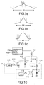
- Figs. 9a to 9c show the continuous S-shape correction according to the change of the horizontal deflection frequency.
- the time point T2 at which the FET is turned from on to off is shifted close to the central portion of the horizontal scanning period (i.e., the turn-off time of the FET 111 is shortened).
- the S-shape correcting capacitors 107 and 110 are connected in parallel to each other at almost greater part of the scanning period, the resonance period of the horizontal deflecting coil is lengthened, so that it is possible to cope with the lower horizontal deflection frequency.
- the time point T2 at which the FET is turned from on to off is set close to the start side of the horizontal scanning period, to increase the time proportion in which the FET 111 is turned off; that is, to shorten the total resonance period for the S-shape correction.
- the horizontal deflection period is shortened to the minimum value th3 as shown in Fig. 9c
- the time point T2 at which the FET is turned from on to off is set further close to the start side of the horizontal scanning period, to turn of f the FET 111 in the greater part of the scanning period.
- the resonance period of the S-shape correction can be decided almost by the capacitor 107.
- Fig. 9a in which the longest horizontal deflection period th1 is shown, it is possible to correct the M-shape distortion effectively by setting the turn-off period of the FET 111 in only the central portion of the horizontal deflection period th1.
- the deflection period is long as shown in Fig. 9c, however, since the S-shape correction can be decided almost all over the scanning period at a single resonance frequency, the M-shape distortion correction effect the same as that shown in Fig. 9a cannot be expected.
- a first embodiment of the S-shape distortion correction circuit according to the present invention will be described hereinbelow with reference to Fig. 10, in which an additional M-shape distortion correction circuit 114 used to switch the S-shape correction is connected.
- the M-shape distortion correction circuit 114 is composed of a second auxiliary S-shape correcting capacitor 115, a second FET 116, a second diode 117 connected to the FET 116, and a second MM 118.
- the FET 111 is turned on or off in the same way as with the case of the example as already explained with reference to Figs. 8a to 8f and Figs. 9a to 9c.
- the output time width of the MM 118 is set in such a way that the FET 116 is turned off at time T4 in the vicinity of the central position of the scanning.
- the auxiliary S-shape capacitor 115 can be separated in the same principle as already explained, a small half sine wave is superposed upon the horizontal deflection signal beginning from time T4, so that it is possible to obtain a more appropriate M-shape distortion correction, even if the period of the horizontal deflection period is short.
- the S-shape correction circuit according to the present invention can easily solve the problem related to inner pin cushion distortion as shown in Fig. 5. For instance, in the example shown in Fig. 7, since the S-shape correction rate can be changed by changing the width tmm of the output pulse of the MM 113, it is possible to correct the pin cushion distortion by modulating the parabolic wave signal with the vertical period by utilizing the above-mentioned change of the S-shape correction rate.
- Fig. 12 shows the voltage Vcs used for correcting the S-shape distortion.
- the output pulse width value tmm is increased in both the upper and lower portions of a screen to decrease the S-shape correction rate of the horizontal deflection.
- the output pulse width value tmm is decreased to widen the region where the resonance capacitance for the S-shape capacitance can be reduced at the central portion along the horizontal direction of the screen.
- Fig. 13 shows an example of the circuit for changing the output pulse width tmm of the MM 113, which is composed of an IC element 130 of the MM 113, a time constant capacitor 120 for deciding the pulse width, a pnp transistor 121 for obtaining a constant current, an emitter resistance 122 of the transistor 121, and a coupling capacitor 123 for applying the parabolic wave signal having the vertical period.
- the output pulse width tmm can be decided by the value of the emitter-collector current Ich of the transistor 121 for charging the time constant capacitor 120. In other words, when the current value Ich is increased, since the charge-up speed of the capacitor 120 increases, the output pulse width tmm is shortened.
- the value obtained by adding the voltage (R x Ich) developed across the resistance 122 to the base-emitter voltage Vbe is equal to a potential difference between the operating supply voltage Ecc of the circuit and the base voltage Eb. Therefore, when the voltage Eb is changed by the external control, since the current value Ich changes according to the voltage Eb, it is possible to change the output pulse width tmm.
- the S-shape correction rate can be changed. Therefore, when this voltage Eb can be obtained by a front-stage horizontal deflection amplitude control circuit (not shown), it is possible to obtain an optimum S-shape correction rate according to the change of the horizontal amplitude. In other words, when the output pulse width tmm is narrowed, the period tdr is lengthened, so that the S-shape correction rate can be increased. In contrast with this, when the horizontal width is required to be reduced, the voltage value Eb is increased, to reduce the S-shape correction rate. As a result, it is possible to always execute an optimum S-shape correction according to the horizontal width value on the basis of the above-mentioned method.
- (d) adjustment can be all combined with each other appropriately as follows: (a) adjustment +(b) adjustment; (a) adjustment +(c) adjustment; (a) adjustment +(d) adjustment; (b) adjustment +(c) adjustment; (b) adjustment +(d) adjustment; (c) adjustment +(d) adjustment; (a) adjustment +(b) adjustment +(c) adjustment; (a) adjustment +(b) adjustment +(d) adjustment; (a) adjustment +(c) adjustment +(d) adjustment; (b) adjustment ⁇ (c) adjustment +(d) adjustment; and (a) adjustment +(b) adjustment +(c) adjustment +(d) adjustment.
- a second embodiment of the horizontal S-shape correction circuit according to the present invention which can correct various horizontal deflection frequencies automatically will be described hereinbelow with reference to Fig. 14.
- a horizontal deflection output circuit 201 is the same as that of the prior art circuit shown in Fig. 6.
- the electron beam of an image receiving tube is deflected in the horizontal direction by passing an S-shape-corrected saw tooth wave current Iy through a series circuit of a horizontal deflection coil 202 and an S-shape correcting capacitor 203.
- the auxiliary S-shape correcting capacitor 205 is constructed by only a single capacitor. That is, the S-shape correcting capacitor group can be constructed by connecting both the S-shape correcting capacitor 203 and the auxiliary S-shape correcting capacitor 205 in series to the horizontal deflecting coil 202.
- the electronic switch element is composed of an electronic switch element (i.e., FET) 206 and a diode 207 connected between the source and the drain of the FET 206.
- a square pulse Vg is applied to the gate of the FET, to switch the turn-on or -off status of the FET in one horizontal deflection period.
- the diode 207 is connected to flow current in a direction opposite to that of the FET 206, when a sufficient current can flow between the drain and the source of the FET 206 in the reverse direction, it is possible to eliminate this diode 207.
- the parabolic voltage wave signal Vpb with the horizontal deflection period develops at one end of the S-shape correcting capacitor 203.
- This voltage signal Vpb is given to a detecting circuit 208, to output a dc voltage Epb according to the amplitude of the voltage Vpb. Further, the voltage signal Epb is applied to one input terminal (non-inversion input terminal) of a succeeding comparator 209. Further, a reference voltage Es is obtained by dividing the dc supply voltage E by two resistors 210 and 211, and then applied to the other input terminal (inversion input terminal) of the comparator 209.
- a pulse Vh related to the horizontal deflection operation is applied to a wave-form shaping circuit 212.
- This pulse Vh can be formed by transforming the horizontal deflection output pulse Vp generated at one end of the horizontal deflecting coil through a fly-back transformer (not shown), for instance.
- a pulse Vt obtained by slicing an apex of the voltage signal Vp (the apex of Vh) is generated from the output of the wave-form shaping circuit 212.
- This pulse Vt is applied to a mono-stable multivibrator (referred to as MM, hereinafter) 213 to trigger the same multivibrator.
- MM mono-stable multivibrator
- the MM 213 outputs a square pulse Vg having a pulse width tg (a suitable or controllable duration time beginning from the trigger time).
- the pulse width tg of this pulse Vg can be controlled by the output voltage Eo of the comparator 209. Therefore, this MM 213 is a timing control circuit for changing the timing at which the electronic switch element (i.e., FET 206) is turned on or off.
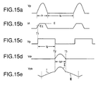
- Fig. 15b shows the trigger pulse Vt applied to the MM 213, which can be obtained, as an appropriate triggering pulse to the MM, by slicing an apex of the horizontal pulse Vh shown in Fig. 15a at a voltage level of E. Since the MM 213 is triggered by the constant level Et of the pulse Vt, it is possible to form a pulse having a pulse width tg beginning from the trigger time T1. Here, since this pulse width tg can be changed according to the voltage Eo as already explained, the fall time T2 of the pulse Vg can be adjusted freely.
- the FET 206 when the FET 206 is turned off and thereby a small pulse Vdr is generated at the drain thereof as shown in Fig. 15d, the voltage Vpb as shown in Fig. 15e is developed at the main S-shape correcting capacitor 203.
- the waveform of the voltage Vpb is of parabolic wave having a small amplitude as shown by I and III in Fig. 15e.
- the voltage V1 across the horizontal deflecting coil 202 represents the differential value (i.e., a gradient) of the current Iy flowing therethrough.
- V1 -Vps during this period ts. Therefore, the voltage value Vpb shown in Fig. 15e represents an opposite-direction gradient of the current Iy of the horizontal deflecting coil. When this voltage Vpb is high, the gradient thereof is large.
- the voltage Vpb as shown in Fig. 15e has two inflection points at times T2 and T3.
- the voltage Vpb represents the gradient of the current Iy as already explained, as far as the voltage value Vpb does not jump before and after times T2 and T3, it is understood that the current Iy can be formed smoothly at almost the same gradient. Therefore, even if an image scrolled in the horizontal direction passes through these points, there exists no such a problem that the image changes abruptly or discontinuously.
- Fig. 16a shows the voltage Vpb required when the horizontal deflection frequency is low or when the period thereof is as long as th.
- the output pulse width of the MM 213 is decided as a relatively long value tg1, and further the timing at which the FET 206 is turned from on to off is delayed during a first half of the horizontal scanning period.
- the turn-off period tdr1 of the FET 206 is shortened.
- the total equivalent capacitance of the S-shape correcting capacitor group must be increased with decreasing horizontal frequency. Therefore, as shown in Fig.
- the time proportion of the turn-off period tdr1 of the FET 206 to the horizontal deflection period th1 is shortened in such a way that two capacitors 203 and 205 are connected in parallel to each other during the major portion of the horizontal scanning period.
- the output pulse width of the MM 213 is shortened as tg2 to increase the proportion of the turn-off period tdr2 to the deflection period th2. Further, when the horizontal deflection frequency increases to near the upper limit, the output pulse width of the MM 213 is shortened as tg3 in such a way the turn-off period tdr3 occupies the major portion of the horizontal deflection period th3.
- the output pulse width tg of the MM 213 is reduced gradually, and thereby the time proportion of the turn-off period tdr of the FET 206 to the horizontal deflection period th is lengthened gradually.
- the time period in which the two capacitors 203 and 205 are connected in parallel to each other during the horizontal scanning period is shortened.
- the value of the output pulse tg of the MM 213 (i.e., the timing at which the FET 206 is turned from on to off) is kept always at an optimum value according to each horizontal deflection frequency.
- the detecting circuit 208 is constructed in such a way that the dc voltage Epb proportional to the amplitude of the voltage Vpb can be obtained.
- a rectifying circuit is suitably used for this detecting circuit 208.
- the circuit is constructed in such a way that when the voltage Epb is increased, the output pulse width tg of the MM 213 can be increased by change of the output voltage Eo of the comparator.
- the comparator output Eo activates the MM 213 so that the period tg can be lengthened.
- the turn-off period tdr is shortened to reduce the amplitude Vpb on the aforementioned principle.
- the amplitude of the voltage Vpb cannot be increased, so that the voltage Epb is kept constant at the same level of the voltage Es.
- the voltage value Vpb across the capacitor 203 projects at the central portion thereof, which is different from the prior art simple parabolic waveform. This implies that it is possible to effectively correct the M-shape distortion (the central portion of an image is shrank), which has been so far difficult to be removed, as far as the parabolic waveform is used.
- Fig. 17 shows a practical example of the MM circuit, by which the output pulse width tg of the MM 213 can be controlled on the basis of the dc voltage Eo.
- This circuit is composed of an MM IC element 214, a time constant capacitor 215 for deciding the pulse width, a pnp transistor 216 for obtaining a constant current, and an emitter resistance 217.
- the output pulse width tg can be decided on the basis of the magnitude of the emitter-collector current Ich of the transistor 216 for charging the time constant capacitor 215. In other words, when the current Ich is increased, since the charge-up speed of the capacitor 215 increases, the output pulse width tg is shortened.
- the value obtained by adding the voltage (R x Ich) developed across the resistance 217 to the base-emitter voltage Vbe of the transistor 216 is equal to a potential difference between the operating supply voltage E of the circuit and the base voltage Eo. Therefore, when the voltage Eo of the comparator output is reduced, since the current Ich increases accordingly, the output pulse width tg can be shortened.
- Fig. 18 shows a practical circuit of the detecting circuit shown in Fig. 14, which is composed of an input capacitor 218, two rectifying diodes 219 and 220, and a smoothing capacitor 221, and two voltage dividing resistors 222 and 223.
- Vpb of the S-shape correcting capacitor 203 When the voltage Vpb of the S-shape correcting capacitor 203 is applied to one end of the input capacitor 218, since the pp value of this waveform is full-wave rectified by the diodes 219 and 220, a dc voltage Erc develops across the smoothing capacitor 221.
- This voltage Erc is divided by the two resistors 222 and 223 into an appropriate value Epb suitable as an input to the succeeding stage comparator 209.
- the time constant decided by the capacitor 221 and the two resistors 222 and 223 it is preferable to set the time constant decided by the capacitor 221 and the two resistors 222 and 223 to a value longer than the vertical deflection period. This is because since the deflecting coil current Iy is usually modulated by the vertical parabolic wave signal due to the correction for the side pin cushion distortion, it is necessary to prevent the components from being superposed upon the voltage Vpb.
- the reference voltage Es shown in Fig. 14 is kept constant, that is, the pp value of the voltage Vpb is kept constant.
- the pp value of the horizontal deflecting coil current Iy is not necessarily constant relative to the horizontal deflection frequency according to the design (i.e., due to the relationship with respect to the blanking time ratio).
- the resistance 224 shown in Fig. since the resistance 224 shown in Fig.
Landscapes
- Engineering & Computer Science (AREA)
- Multimedia (AREA)
- Signal Processing (AREA)
- Details Of Television Scanning (AREA)
Claims (2)
- Horizontale S-Form-Korrekturschaltung, die folgendes umfasst:dadurch gekennzeichnet, dass sie ferner folgendes umfasst:eine S-Form-Korrektur-Kondensatorgruppe (203, 205), die in Reihe mit einer horizontalen Ablenkspule (202) geschaltet ist;ein elektronisches Schaltelement (206, 207) zum Steuern des Anschlusses eines Teils von Kondensatoren der genannten S-Form-Korrektur-Kondensatorgruppe auf eine solche Weise, dass sie in einer ersten Hälfte einer horizontalen Abtastperiode ausgeschaltet und in einer horizontalen Austastperiode eingeschaltet werden; undeine Zeitsteuerschaltung (213) zum Einstellen des Zeitpunktes, zu dem das genannte elektronische Schaltelement in der ersten Hälfte der horizontalen Abtastperiode ausgeschaltet wird;wobei die genannte Zeitsteuerschaltung auf einen Ausgang der genannten Vergleichsschaltung anspricht.eine Detektorschaltung (208) zum Erfassen einer Amplitude einer Wellenform eines Signals, das von der genannten S-Form-Korrektur-Kondensatorgruppe erzeugt wird; undeine Vergleichsschaltung (209) zum Vergleichen eines Ausgangs der genannten Detektorschaltung mit einer Referenzspannung;
- Horizontale S-Form-Korrekturschaltung nach Anspruch 1, wobei die Referenzspannung gemäß einer horizontalen Ablenkfrequenz geändert wird.
Applications Claiming Priority (6)
| Application Number | Priority Date | Filing Date | Title |
|---|---|---|---|
| JP224514/96 | 1996-08-07 | ||
| JP22451496 | 1996-08-07 | ||
| JP22451496 | 1996-08-07 | ||
| JP255434/96 | 1996-09-05 | ||
| JP25543496A JP3310177B2 (ja) | 1996-09-05 | 1996-09-05 | 水平s字補正回路 |
| JP25543496 | 1996-09-05 |
Publications (3)
| Publication Number | Publication Date |
|---|---|
| EP0823812A2 EP0823812A2 (de) | 1998-02-11 |
| EP0823812A3 EP0823812A3 (de) | 1998-03-18 |
| EP0823812B1 true EP0823812B1 (de) | 2002-04-10 |
Family
ID=26526108
Family Applications (1)
| Application Number | Title | Priority Date | Filing Date |
|---|---|---|---|
| EP97305691A Expired - Lifetime EP0823812B1 (de) | 1996-08-07 | 1997-07-29 | Horizontale S-Form-Korrektionsschaltung |
Country Status (3)
| Country | Link |
|---|---|
| US (1) | US5962993A (de) |
| EP (1) | EP0823812B1 (de) |
| DE (1) | DE69711783D1 (de) |
Cited By (3)
| Publication number | Priority date | Publication date | Assignee | Title |
|---|---|---|---|---|
| US6624597B2 (en) | 1997-08-26 | 2003-09-23 | Color Kinetics, Inc. | Systems and methods for providing illumination in machine vision systems |
| US7652436B2 (en) | 2000-09-27 | 2010-01-26 | Philips Solid-State Lighting Solutions, Inc. | Methods and systems for illuminating household products |
| US7845823B2 (en) | 1997-08-26 | 2010-12-07 | Philips Solid-State Lighting Solutions, Inc. | Controlled lighting methods and apparatus |
Families Citing this family (19)
| Publication number | Priority date | Publication date | Assignee | Title |
|---|---|---|---|---|
| US6781329B2 (en) | 1997-08-26 | 2004-08-24 | Color Kinetics Incorporated | Methods and apparatus for illumination of liquids |
| US6717376B2 (en) | 1997-08-26 | 2004-04-06 | Color Kinetics, Incorporated | Automotive information systems |
| US20030133292A1 (en) | 1999-11-18 | 2003-07-17 | Mueller George G. | Methods and apparatus for generating and modulating white light illumination conditions |
| US6548967B1 (en) | 1997-08-26 | 2003-04-15 | Color Kinetics, Inc. | Universal lighting network methods and systems |
| US7764026B2 (en) | 1997-12-17 | 2010-07-27 | Philips Solid-State Lighting Solutions, Inc. | Systems and methods for digital entertainment |
| US6774584B2 (en) | 1997-08-26 | 2004-08-10 | Color Kinetics, Incorporated | Methods and apparatus for sensor responsive illumination of liquids |
| US6777891B2 (en) | 1997-08-26 | 2004-08-17 | Color Kinetics, Incorporated | Methods and apparatus for controlling devices in a networked lighting system |
| US6222328B1 (en) * | 1998-04-21 | 2001-04-24 | Sony Corporation | Horizontal deflection circuit |
| JP3832090B2 (ja) * | 1998-05-07 | 2006-10-11 | ソニー株式会社 | 水平偏向回路 |
| JPH11355601A (ja) * | 1998-06-05 | 1999-12-24 | Sony Corp | 水平偏向回路 |
| EP1042780B1 (de) | 1998-06-05 | 2004-08-04 | Koninklijke Philips Electronics N.V. | Ablenkkorrektur |
| WO2001026360A1 (en) * | 1999-10-01 | 2001-04-12 | Koninklijke Philips Electronics N.V. | Dynamic s-correction |
| JP3369535B2 (ja) * | 1999-11-09 | 2003-01-20 | 松下電器産業株式会社 | プラズマディスプレイ装置 |
| PT1422975E (pt) | 2000-04-24 | 2010-07-09 | Philips Solid State Lighting | Produto base de leds |
| US6801003B2 (en) | 2001-03-13 | 2004-10-05 | Color Kinetics, Incorporated | Systems and methods for synchronizing lighting effects |
| US6570777B1 (en) * | 2001-12-06 | 2003-05-27 | Eni Technology, Inc. | Half sine wave resonant drive circuit |
| WO2004100624A2 (en) | 2003-05-05 | 2004-11-18 | Color Kinetics, Inc. | Lighting methods and systems |
| EP1681847A1 (de) * | 2005-01-12 | 2006-07-19 | Videocolor S.p.A. | Vorrichtung zur Korrektur der horizontalen Bildverzerrung und diese enthaltende Bildanzeigevorrichtung |
| US10321528B2 (en) | 2007-10-26 | 2019-06-11 | Philips Lighting Holding B.V. | Targeted content delivery using outdoor lighting networks (OLNs) |
Family Cites Families (15)
| Publication number | Priority date | Publication date | Assignee | Title |
|---|---|---|---|---|
| US4501995A (en) * | 1982-04-06 | 1985-02-26 | Tektronix, Inc. | Automatic "S" correction circuit |
| US4533855A (en) * | 1983-12-16 | 1985-08-06 | Rca Corporation | Switched capacitor S-correction circuit |
| JPH0646786B2 (ja) * | 1985-04-19 | 1994-06-15 | ソニー株式会社 | マルチ走査形テレビジヨン受像機の水平偏向回路 |
| US4709193A (en) * | 1986-05-30 | 1987-11-24 | Rca Corporation | S-capacitance switching circuit for a video display |
| FR2603442B1 (fr) * | 1986-09-02 | 1988-11-10 | Radiotechnique Ind & Comm | Circuit de balayage lignes avec correction dynamique de s |
| JPH0748805B2 (ja) * | 1990-05-28 | 1995-05-24 | 三菱電機株式会社 | オート・トラッキング・モニタのs字補正コンデンサ切替装置 |
| DE4136178A1 (de) * | 1991-11-02 | 1993-05-06 | Deutsche Thomson-Brandt Gmbh, 7730 Villingen-Schwenningen, De | Schaltung zur kontinuierlichen zoom-einstellung der bildbreite in einem fernsehempfaenger |
| DE4142651A1 (de) * | 1991-12-21 | 1993-07-01 | Philips Broadcast Television S | Schaltung zur h-ablenkung fuer fernsehbild-wiedergabegeraete |
| GB9401364D0 (en) * | 1994-01-25 | 1994-03-23 | Rca Thomson Licensing Corp | Deflection circuits with distortion correction |
| JPH07326302A (ja) * | 1994-05-30 | 1995-12-12 | Mitsubishi Electric Corp | ディスプレイモニタ装置のs字補正コンデンサ切替装置 |
| DE69513379T2 (de) * | 1994-08-18 | 2000-05-11 | Koninkl Philips Electronics Nv | Schaltvorrichtung für s-korrektur-kondensatoren |
| JPH0879554A (ja) * | 1994-09-06 | 1996-03-22 | Hitachi Ltd | S字補正回路 |
| JPH08204982A (ja) * | 1995-01-23 | 1996-08-09 | Totoku Electric Co Ltd | S字補正調整回路 |
| FR2738976A1 (fr) * | 1995-09-20 | 1997-03-21 | Philips Electronics Nv | Circuit de balayage horizontal de television muni d'une capacite de s commutee par un thyristor |
| JP3538997B2 (ja) * | 1995-09-22 | 2004-06-14 | ソニー株式会社 | 水平偏向回路 |
-
1997
- 1997-07-29 EP EP97305691A patent/EP0823812B1/de not_active Expired - Lifetime
- 1997-07-29 DE DE69711783T patent/DE69711783D1/de not_active Expired - Lifetime
- 1997-08-06 US US08/906,856 patent/US5962993A/en not_active Expired - Fee Related
Cited By (3)
| Publication number | Priority date | Publication date | Assignee | Title |
|---|---|---|---|---|
| US6624597B2 (en) | 1997-08-26 | 2003-09-23 | Color Kinetics, Inc. | Systems and methods for providing illumination in machine vision systems |
| US7845823B2 (en) | 1997-08-26 | 2010-12-07 | Philips Solid-State Lighting Solutions, Inc. | Controlled lighting methods and apparatus |
| US7652436B2 (en) | 2000-09-27 | 2010-01-26 | Philips Solid-State Lighting Solutions, Inc. | Methods and systems for illuminating household products |
Also Published As
| Publication number | Publication date |
|---|---|
| EP0823812A3 (de) | 1998-03-18 |
| EP0823812A2 (de) | 1998-02-11 |
| US5962993A (en) | 1999-10-05 |
| DE69711783D1 (de) | 2002-05-16 |
Similar Documents
| Publication | Publication Date | Title |
|---|---|---|
| EP0823812B1 (de) | Horizontale S-Form-Korrektionsschaltung | |
| EP0146345B1 (de) | S-Korrekturschaltung mit geschaltetem Kondensator | |
| JP2944663B2 (ja) | ビデオ表示装置 | |
| JP3617669B2 (ja) | テレビジョン偏向装置 | |
| US4516058A (en) | Linearity corrected horizontal deflection circuit | |
| JP2716495B2 (ja) | 画像管用の偏向回路 | |
| US4868464A (en) | Linearity correction circuit for television receiver | |
| US4225809A (en) | Side pincushion correction circuit | |
| US6300731B1 (en) | Dynamic focus voltage amplitude controller | |
| EP0664644A2 (de) | Schaltung zur Korrektur von Rasterverzerrungen im inneren Teil des Bildes | |
| EP1135927B1 (de) | Dynamische s-korrektur | |
| JP3310177B2 (ja) | 水平s字補正回路 | |
| EP0530809B2 (de) | Ablenkstromerzeugungsschaltungen | |
| JPH09331466A (ja) | 水平直線性補正回路 | |
| KR100499991B1 (ko) | 래스터보정을갖는수평편향회로 | |
| US6256074B1 (en) | Control signal generator for dynamic focus disabling | |
| JP3479089B2 (ja) | テレビジョン偏向装置 | |
| JP3832090B2 (ja) | 水平偏向回路 | |
| JP3538997B2 (ja) | 水平偏向回路 | |
| JPH08237674A (ja) | コンバーゼンス補正装置 | |
| JPH10108036A (ja) | 水平s字補正回路 | |
| GB2098424A (en) | Horizontal driver and linearity circuit | |
| JP3077159B2 (ja) | ダイナミックフォーカス回路 | |
| EP1091569A2 (de) | Schaltung zur Korrektur von Rasterverzerrungen | |
| JP2000165698A (ja) | ビデオ・イメ―ジング装置 |
Legal Events
| Date | Code | Title | Description |
|---|---|---|---|
| PUAI | Public reference made under article 153(3) epc to a published international application that has entered the european phase |
Free format text: ORIGINAL CODE: 0009012 |
|
| PUAL | Search report despatched |
Free format text: ORIGINAL CODE: 0009013 |
|
| AK | Designated contracting states |
Kind code of ref document: A2 Designated state(s): DE FR GB |
|
| AK | Designated contracting states |
Kind code of ref document: A3 Designated state(s): AT BE CH DE DK ES FI FR GB GR IE IT LI LU MC NL PT SE |
|
| 17P | Request for examination filed |
Effective date: 19980409 |
|
| AKX | Designation fees paid |
Free format text: DE FR GB |
|
| RBV | Designated contracting states (corrected) |
Designated state(s): DE FR GB |
|
| 17Q | First examination report despatched |
Effective date: 20000105 |
|
| GRAG | Despatch of communication of intention to grant |
Free format text: ORIGINAL CODE: EPIDOS AGRA |
|
| GRAG | Despatch of communication of intention to grant |
Free format text: ORIGINAL CODE: EPIDOS AGRA |
|
| GRAH | Despatch of communication of intention to grant a patent |
Free format text: ORIGINAL CODE: EPIDOS IGRA |
|
| REG | Reference to a national code |
Ref country code: GB Ref legal event code: IF02 |
|
| GRAH | Despatch of communication of intention to grant a patent |
Free format text: ORIGINAL CODE: EPIDOS IGRA |
|
| GRAA | (expected) grant |
Free format text: ORIGINAL CODE: 0009210 |
|
| AK | Designated contracting states |
Kind code of ref document: B1 Designated state(s): DE FR GB |
|
| PG25 | Lapsed in a contracting state [announced via postgrant information from national office to epo] |
Ref country code: FR Free format text: LAPSE BECAUSE OF FAILURE TO SUBMIT A TRANSLATION OF THE DESCRIPTION OR TO PAY THE FEE WITHIN THE PRESCRIBED TIME-LIMIT Effective date: 20020410 |
|
| REF | Corresponds to: |
Ref document number: 69711783 Country of ref document: DE Date of ref document: 20020516 |
|
| PG25 | Lapsed in a contracting state [announced via postgrant information from national office to epo] |
Ref country code: DE Free format text: LAPSE BECAUSE OF FAILURE TO SUBMIT A TRANSLATION OF THE DESCRIPTION OR TO PAY THE FEE WITHIN THE PRESCRIBED TIME-LIMIT Effective date: 20020711 |
|
| EN | Fr: translation not filed | ||
| PLBE | No opposition filed within time limit |
Free format text: ORIGINAL CODE: 0009261 |
|
| STAA | Information on the status of an ep patent application or granted ep patent |
Free format text: STATUS: NO OPPOSITION FILED WITHIN TIME LIMIT |
|
| 26N | No opposition filed |
Effective date: 20030113 |
|
| PGFP | Annual fee paid to national office [announced via postgrant information from national office to epo] |
Ref country code: GB Payment date: 20060726 Year of fee payment: 10 |
|
| GBPC | Gb: european patent ceased through non-payment of renewal fee |
Effective date: 20070729 |
|
| PG25 | Lapsed in a contracting state [announced via postgrant information from national office to epo] |
Ref country code: GB Free format text: LAPSE BECAUSE OF NON-PAYMENT OF DUE FEES Effective date: 20070729 |