EP0815529B1 - Connector for a smart card reader apparatus - Google Patents
Connector for a smart card reader apparatus Download PDFInfo
- Publication number
- EP0815529B1 EP0815529B1 EP96908168A EP96908168A EP0815529B1 EP 0815529 B1 EP0815529 B1 EP 0815529B1 EP 96908168 A EP96908168 A EP 96908168A EP 96908168 A EP96908168 A EP 96908168A EP 0815529 B1 EP0815529 B1 EP 0815529B1
- Authority
- EP
- European Patent Office
- Prior art keywords
- card
- contact
- brush
- connector
- potential
- Prior art date
- Legal status (The legal status is an assumption and is not a legal conclusion. Google has not performed a legal analysis and makes no representation as to the accuracy of the status listed.)
- Expired - Lifetime
Links
Images


Classifications
-
- G—PHYSICS
- G06—COMPUTING; CALCULATING OR COUNTING
- G06K—GRAPHICAL DATA READING; PRESENTATION OF DATA; RECORD CARRIERS; HANDLING RECORD CARRIERS
- G06K7/00—Methods or arrangements for sensing record carriers, e.g. for reading patterns
- G06K7/06—Methods or arrangements for sensing record carriers, e.g. for reading patterns by means which conduct current when a mark is sensed or absent, e.g. contact brush for a conductive mark
-
- G—PHYSICS
- G06—COMPUTING; CALCULATING OR COUNTING
- G06K—GRAPHICAL DATA READING; PRESENTATION OF DATA; RECORD CARRIERS; HANDLING RECORD CARRIERS
- G06K7/00—Methods or arrangements for sensing record carriers, e.g. for reading patterns
- G06K7/0013—Methods or arrangements for sensing record carriers, e.g. for reading patterns by galvanic contacts, e.g. card connectors for ISO-7816 compliant smart cards or memory cards, e.g. SD card readers
- G06K7/0056—Methods or arrangements for sensing record carriers, e.g. for reading patterns by galvanic contacts, e.g. card connectors for ISO-7816 compliant smart cards or memory cards, e.g. SD card readers housing of the card connector
- G06K7/0069—Methods or arrangements for sensing record carriers, e.g. for reading patterns by galvanic contacts, e.g. card connectors for ISO-7816 compliant smart cards or memory cards, e.g. SD card readers housing of the card connector including means for detecting correct insertion of the card, e.g. end detection switches notifying that the card has been inserted completely and correctly
-
- G—PHYSICS
- G06—COMPUTING; CALCULATING OR COUNTING
- G06K—GRAPHICAL DATA READING; PRESENTATION OF DATA; RECORD CARRIERS; HANDLING RECORD CARRIERS
- G06K7/00—Methods or arrangements for sensing record carriers, e.g. for reading patterns
- G06K7/0013—Methods or arrangements for sensing record carriers, e.g. for reading patterns by galvanic contacts, e.g. card connectors for ISO-7816 compliant smart cards or memory cards, e.g. SD card readers
- G06K7/0021—Methods or arrangements for sensing record carriers, e.g. for reading patterns by galvanic contacts, e.g. card connectors for ISO-7816 compliant smart cards or memory cards, e.g. SD card readers for reading/sensing record carriers having surface contacts
Definitions
- the invention relates to a connector for a card reader device. microcircuit.
- the term “card” means all kinds of cards of the type incorporating a monolithic or hybrid integrated circuit, known as a "chip".
- This term “microcircuit” will be used in the following. This is, for example, format card “credit card”, also known under the name “CAM” (Carte A Mémoire "). Most often, the microcircuit is produced on the basis of a microprocessor or a microcontroller, comprising, in particular memory circuits, for example of "PROM” type. This type of card must be able to be inserted into devices specific reading and / or writing of data. To simplify this device will called “reader” in the following, it being understood that it can also ensure writing data and other related functions (power supply electrical, tests) which will be recalled below.
- the data is stored in the aforementioned memory circuits, generally in encrypted form. They are therefore read at from memory positions or on the contrary written in these memory positions.
- the first category consists of detection systems electronic.
- an electrical test is carried out, for example the resistance measurement between the brush contacts. If these tests do not match expected values, in a given range, it is deduced from this that the card is inserted incorrectly or that an object stranger is introduced in his place.
- the second category consists of so-called "to landing".
- An example of such a system is described in the patent application French FR-A-2 628 901.
- the card is positioned against a stop before contacting the brushes. Contact is made by relative displacement from the card to the brushes, perpendicular to the surface of the card (faces main).
- Safety can only be ensured by the proper functioning of mechanical organs of the system. They can however be doubled by a typical contact "limit switch” which blocks the power-up sequence in case the card does not would not be in the correct position.
- a power-up sequence can be ensured by the height of the brushes, or by an initialization of the electronics by closing of a "card presence” contact.
- the main drawback is that the arrangement mechanics required to perform the above functions is complex and expensive.
- the third category consists of brush contact systems rubbing with "limit switch" contact. Such a system is disclosed, for example, by French patent application FR-A-2 623 314.
- the connectors in which are cards inserted have a "limit switch” contact which triggers the bet on the microcircuit when the card is in the correct position.
- the mechanical arrangement is simple and inexpensive.
- the invention sets itself the goal to provide a solution to the problems mentioned above, while alleviating the drawbacks of known art systems, some of which have just been mentioned.
- the reading frame according to the invention thus comprises in combination, an electronic circuit as described in the patent application WO-A-96/24 111, as well as a brush contact additional, as described in EP-A-0 595 305.
- this brush contact instead of being additional, is a single contact element assigned to one of said ranges of contact which is offset from the brush contacts assigned to the other ranges of contact.
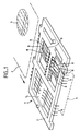
- the connector 1 for a microcircuit card reader device C 3 comprises a body 2 supporting brush contact elements B, intended to be brought into electrical contact with conductive pads associated with said microcircuit I C when the card C is inserted in connector 1.
- this connector 1 comprises an electronic circuit I C connected, on the one hand, with at least part of said brush contact elements C 1 to C 8 and, on the other hand, with the electronic circuit 4 of the card reader.
- the electronic circuit I C carried by the connector 1 comprises means which are detailed in PCT application No. FR 96/00156 for controlling operations of insertion or removal of the card C in the card reader.
- FIG. 2 illustrates a fragment of card C conforming to standard ISO 7816.
- This standard prescribes the dimensions, the location and the allocation of the contact pads, C 1 to C 8 , flush with the surface of microcircuit type cards. ID-1.
- the card can include one or more microcircuits. The input-output terminals of these microcircuits are connected to these contact pads, C 1 to C 8 .
- the contact pads, C 1 to C 8 are organized in two rows of four pads, respectively C 1 to C 4 and C 5 to C 8 , substantially parallel to each other and parallel to the left edge B G (in the figure) of card C, edge serving as a stop.
- the figure also represents the upper edge B S of the card C.
- the main geometric characteristics defining the contacts, C 1 to C 8 expressed in minimum and maximum distances (in mm) such as 'they appear from the above-mentioned standard.
- each conductive zone must include a substantially rectangular surface with minimum dimensions 1.7 ⁇ 2mm. Maximum dimensions are not specified. It is only indicated that each contact must be electrically isolated from the other contacts.
- the surface of the card C, between contact areas C 1 to C 8 can be insulating or conductive: for example covered with a metallization connected to the ground contact, for the purpose of decoupling.
- FIG. 3 illustrates an example of a microcircuit card C, in accordance with the AFNOR standard, older, under the same representation conditions as the card C.
- the contact C 8 in the case of the ISO card, is in place of the contact C 1 , in the case of the AFNOR card.
- the connector used in the card reader must take into account the standard used, this constraint being common to known art connectors.
- the edges of the pads of the "signal" contacts (that is to say other than C 1 and C 5 ) are aligned with the pads of contacts C 1 / C 5 or offset in the favorable direction, which is the most general case.
- FIG. 4 which again represents a card C conforming to the aforementioned ISO standard.
- the contact area C 1 supply voltage
- the contact area C 1 has an elongated shape and extends in the direction of the area C 5 .
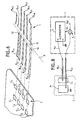
- Figures Sa and 5b represent, by way of example, an Art Connu connector, designated under the general reference 60, seen in section BB and high, respectively.
- the contact elements forming brushes, shown under the general reference 50 and folded at 63, are arranged in two rows in lights 66 and 67, respectively. It also has a pair of elements of contacts 20-30, called "limit switch" detection, folded at 60 and 61. These elements 20 and 30 are arranged in a hole 68 and their ends folded in a 68 'light.
- the front edge 70 (top of FIG. 5b), which is curved, has two lateral end points 71. These two points 71 define a stop line BB for the card.
- the region 24 of the contact element 20, located near the stop line BB has a butt-shaped profile.
- the invention is capable of two main embodiments.
- a contact element is added additional of the type “tension brushes”, which comes in parallel with the “brushes of voltage "normal, according to a configuration which will be described below.
- This brushes additional is notably offset from the normal brush.
- the contact element of the type "tension brushes" is not doubled but only offset from the row contact elements to which it belongs.
- FIG. 6 schematically illustrates a connector 1 for inserting card C according to the first embodiment of the invention.
- the card C to be inserted in the connector 1 meets the aforementioned ISO standard.
- FIG. 6 For clarity, only FIG. 6 have been shown in FIG. of contact and their arrangements in space.
- body of the connector and other accessories may be fully common to connectors of Known Art, for example to the connector shown in Figures 5a and 5b.
- the connector 1 comprises two rows of contact elements, forming brushes, respectively B C1 B C4 and B C5 -B C8 , four in each row.
- Each of these brushes is intended to be brought into galvanic contact with a corresponding area, C 1 to C 8 , of the card C. They play the role of the contact elements 50 of FIG. 5a.
- a pair of contact elements, B fc1 and B fc2 called “limit switches ", intended to detect the complete and correct insertion of the card C into the connector 1 can be provided. .
- the brushes, B C1 -B C4 and B C5 -B C8 are made of metal blades, thin and flexible, whose distal ends 10 to 80 have the shape of a stick. These blades are parallel to each other and the aforementioned distal ends are arranged opposite, two by two, on either side of an axis of symmetry A perpendicular to the blades.
- an additional contact element referenced B CX, is provided , doubling the contact element B C1 , of the "tension brushes" type.
- This additional contact element B CX can moreover be cut out ( at the time of manufacture of the connector) in the same strip as the normal contacts and overmolded at the same time as them in the body of the connector (see Figure 5b). It will be advantageous, in this case, to narrow the width of a blade and add a fifth next.
- This additional contact element B CX makes it possible to detect the insertion, as the removal of the card C and, therefore, to connect or cut the electrical energy supply, as will be explained below.
- FIG. 7a illustrates the position of the brush contact elements B C1 and B CX , with respect to the range C 1 , in the normal working position, that is to say ie card C correctly inserted in connector 1.
- the brush contact element B CX is in front of the brush contact element B C1 , but outside the range C 1 .
- the brush contact element B C1 is supplied by the supply voltage V CC , generally + 5 V.
- the range C 1 is then also brought to this potential and the microcircuit of the card C (not shown) supplied with electrical energy. Read and / or read operations can take place normally.
- FIG. 8 schematically illustrates, in the form of a block diagram, an electronic circuit for managing the state of the contact elements B C1 and B CX .
- the contact element B C1 is connected to the output V CC of a regulated electrical supply 2 disposed in the reader L.
- the additional contact element B CX is connected to the input of a circuit 3, comprising for example a voltage comparator, between V CC and a reference voltage V ref , for example 0 V, the range M being assumed to be grounded. In reality any reference voltage may be suitable, the role of the comparison circuit 3 being to detect a variation in the potential of the additional contact element B CX , of amplitude greater than a determined threshold. This threshold takes into account, in particular, the tolerances of the supply voltage, foreseeable noise, etc.
- the power supply 2 is provided with electronic circuits detecting a short-circuiting of the output (earthing of the voltage V DC ) and cutting it off. This operation will be performed for the detection of the event "a /" recalled above: detection of a short circuit.
- the detection of the event "b /" (modification of the potential of the additional brush contact element B CX ) is carried out by the comparator circuit 3.
- the output signal V S is transmitted on an input of the supply 2 and blocks this (switching off the brush contact element B C1 ) when a potential change of predetermined amplitude is detected.
- This output signal V S can also be transmitted to an electronic system to deactivate the signal brushes.
- FIG. 7c also illustrates a situation of withdrawal of the card C arte , but in this example, the mass range M (FIGS. 7a and 7b) does not exist.
- the comparator 3 FIG. 8
- the additional contact element B CX goes to the potential V CC .
- FIG. 9a illustrates the configuration to be adopted for the case of a card C according to the AFNOR standard.
- the stop (not shown) is on the side opposite the range C 1 . More specifically, this figure illustrates the normal working state.
- the additional contact element C BX is offset in front of the contact element C B1 , but rests on the pad C 1 .
- the two contact elements C BX and C B1 are therefore brought to the same potential V CC . It is also assumed that a mass range, formed by the range C 5 , adjoins the range C 1 .
- the mass range C 5 will approach the additional contact element C BX , as illustrated in FIG. 9b.
- the contact element B C1 is offset on the abutment side with respect to the contact elements of the "signal brushes" type. If we refer again to Figures 9a to 9c, we have the contact element B C1 in place of the additional contact element B CX .
- This arrangement ensures correct sequencing, by cutting the power supply, possibly after it has been short-circuited.
- the main advantage of the second embodiment is naturally that it is not necessary to provide electronics for managing the state of the brushes. In addition, only a slight modification of the contact element B C1 is necessary.
- the center of the range C 1 is at a distance equal to 18.87 mm from the stop card b, with a tolerance of +0.4 mm maximum and -0.5 mm maximum.
- the width of the range C 1 in a direction parallel to F R , is at least 2 mm and the distance separating a range contiguous to C 1 and C 1 is 0.2 mm.
- the space requirement may be less than that of the connectors equivalents of known art, because the contact elements of the "limit switch" type can be omitted, which allows a possible reduction in thickness.
Landscapes
- Engineering & Computer Science (AREA)
- Artificial Intelligence (AREA)
- Computer Vision & Pattern Recognition (AREA)
- Physics & Mathematics (AREA)
- General Physics & Mathematics (AREA)
- Theoretical Computer Science (AREA)
- Coupling Device And Connection With Printed Circuit (AREA)
- Details Of Connecting Devices For Male And Female Coupling (AREA)
Abstract
Description
L'invention concerne un connecteur pour appareil lecteur de carte à microcircuit.The invention relates to a connector for a card reader device. microcircuit.
Dans le cadre de l'invention, on entend par "carte" toutes sortes de cartes du type incorporant un circuit intégré monolithique ou hybride, dit "puce". Ce terme "microcircuit" sera utilisé dans ce qui suit. Il s'agit, par exemple, de carte du format "carte de crédit", connue encore sous la dénomination "CAM" (Carte A Mémoire"). Le plus souvent, le microcircuit est réalisé à base d'un microprocesseur ou d'un microcontrôleur, comprenant, notamment des circuits de mémoire, par exemple de type "PROM". Ce type de carte doit pouvoir être inséré dans des dispositifs spécifiques de lecture et/écriture de données. Pour simplifier ce dispositif sera appelé "lecteur" dans ce qui suit, étant bien entendu qu'il peut également assurer l'écriture de données et d'autres fonctions annexes (alimentation en énergie électrique, tests) qui seront rappelées ci-après. Les données sont stockées dans les circuits mémoires précités, généralement sous forme cryptée. Elles sont donc lues à partir de positions mémoires ou au contraires écrites dans ces positions mémoires.In the context of the invention, the term "card" means all kinds of cards of the type incorporating a monolithic or hybrid integrated circuit, known as a "chip". This term "microcircuit" will be used in the following. This is, for example, format card "credit card", also known under the name "CAM" (Carte A Mémoire "). Most often, the microcircuit is produced on the basis of a microprocessor or a microcontroller, comprising, in particular memory circuits, for example of "PROM" type. This type of card must be able to be inserted into devices specific reading and / or writing of data. To simplify this device will called "reader" in the following, it being understood that it can also ensure writing data and other related functions (power supply electrical, tests) which will be recalled below. The data is stored in the aforementioned memory circuits, generally in encrypted form. They are therefore read at from memory positions or on the contrary written in these memory positions.
D'autres architectures logiques sont mise en oeuvre, notamment pour des applications type "porte-monnaie électronique" ou similaire.Other logical architectures are implemented, in particular for "electronic wallet" or similar applications.
Dans tous les cas, il existe des organes d'entrée-sortie constitués par des plages de contact, encore appelés "pads", affleurant en surface d'une des faces principales de la carte. Diverses normes définissent la position de ces plages de contact (ISO, AFNOR, etc.). Ils servent, non seulement pour les entrées-sorties de données précitées, mais aussi pour l'alimentation en énergie électrique du microcircuit ainsi que pour effectuer diverses vérifications, selon les applications considérées (test de présence, etc.). Le lecteur comporte des contacts balais qui viennent en contact galvanique avec les plages précitées, lorsque la carte est correctement insérée dans un connecteur prévu à cet effet.In all cases, there are input-output members constituted by contact pads, also called "pads", flush on the surface of one of the faces main map. Various standards define the position of these ranges of contact (ISO, AFNOR, etc.). They are used not only for the input-output of aforementioned data, but also for the supply of electrical energy to the microcircuit as well as to carry out various verifications, depending on the applications considered (presence test, etc.). The reader has brush contacts which come into galvanic contact with the aforementioned areas, when the card is correctly inserted into a connector provided for this purpose.
Divers besoins et tendances émergent actuellement, et parmi ceux-ci, les suivants :
- nécessité d'améliorer la sécurité de fonctionnement des appareils lecteurs de carte ;
- tendance à la miniaturisation, donc à la diminution de l'épaisseur des lecteurs de carte ;
- et multiplication des applications de la carte à microcircuit, ainsi qu'une baisse rapide des prix des connecteurs, en fonction directe de la croissance du marché correspondant.
- the need to improve the operational safety of card reader devices;
- tendency to miniaturization, therefore to decrease the thickness of card readers;
- and multiplication of microcircuit card applications, as well as a rapid fall in connector prices, as a direct function of the growth of the corresponding market.
En conséquence, un certain nombre de problèmes doivent être résolus
simultanément, dont les suivants :
Dans tous ces cas, il est nécessaire de bloquer le fonctionnement du lecteur et couper l'alimentation en énergie électrique pour limiter les risques de détérioration des circuits et/ou tentatives de fraude.In all these cases, it is necessary to block the operation of the drive and cut off the power supply to limit the risk of deterioration of circuits and / or fraud attempts.
Il existe de nombreux système de lecteur visant à résoudre tout ou partie de ces problèmes. Il est possible de les classer en trois grandes catégories.There are many reader systems aimed at solving all or part of these problems. It is possible to classify them into three main categories.
La première catégorie est constituée par des systèmes de détection électronique.The first category consists of detection systems electronic.
Dans ce type de systèmes, avant d'envoyer une tension électrique au microcircuit, on procède à un test électrique, par exemple la mesure de la résistance entre les contacts balais. Si ces tests ne correspondent pas à des valeurs prévues, dans une gamme donnée, il en est déduit que la carte est mal insérée ou qu'un objet étranger est introduit à sa place.In this type of system, before sending an electrical voltage to the microcircuit, an electrical test is carried out, for example the resistance measurement between the brush contacts. If these tests do not match expected values, in a given range, it is deduced from this that the card is inserted incorrectly or that an object stranger is introduced in his place.
Ce type de système comporte plusieurs inconvénients et parmi lesquels, les suivants :
- Le système devrait fonctionner pour tous les types de microcircuits dont sont équipées les cartes du marché, du moins pour une application donnée (cartes bancaires, etc.). Or la variété de microcircuits est trop importante pour permettre une procédure simple et unique.
- La détection s'effectue juste au passage entre une zone interdite et une zone de fonctionnement. Il est aisé de comprendre, qu'en cas d'arrachement, le système doit réagir très rapidement. L'électronique appropriée à cette fonction est complexe et donc coûteuse.
- The system should work for all types of microcircuits with which market cards are fitted, at least for a given application (bank cards, etc.). However, the variety of microcircuits is too great to allow a simple and unique procedure.
- Detection is carried out just at the passage between a prohibited zone and an operating zone. It is easy to understand that in the event of a wrench, the system must react very quickly. The appropriate electronics for this function are complex and therefore expensive.
La deuxième catégorie est constituée par des systèmes dits "à atterrissage". Un exemple d'un tel système est décrit dans la demande de brevet français FR-A-2 628 901.The second category consists of so-called "to landing ". An example of such a system is described in the patent application French FR-A-2 628 901.
Conformément à ces systèmes, la carte est positionnée contre une butée avant mise en contact avec les balais. Le contact s'effectue par déplacement relatif de la carte vers les balais, perpendiculairement à la surface de la carte (faces principales).According to these systems, the card is positioned against a stop before contacting the brushes. Contact is made by relative displacement from the card to the brushes, perpendicular to the surface of the card (faces main).
La sécurité peut n'être assurée que par le bon fonctionnement des organes mécaniques du système. On peut cependant les doubler par un contact type "fin de course" qui bloque la séquence de mise sous tension au cas où la carte ne serait pas en position correcte. Un séquencement de la mise sous tension peut être assurée par la hauteur des balais, ou par une initialisation de l'électronique par fermeture d'un contact "présence carte".Safety can only be ensured by the proper functioning of mechanical organs of the system. They can however be doubled by a typical contact "limit switch" which blocks the power-up sequence in case the card does not would not be in the correct position. A power-up sequence can be ensured by the height of the brushes, or by an initialization of the electronics by closing of a "card presence" contact.
Le principal inconvénient est constitué par le fait que l'agencement mécanique nécessaire pour réaliser les fonctions précitées est complexe et coûteux.The main drawback is that the arrangement mechanics required to perform the above functions is complex and expensive.
La troisième catégorie est constituée par des systèmes à contact balais frottants avec contact de "fin de course". Un tel système est divulgué, par exemple, par la demande de brevet français FR-A-2 623 314.The third category consists of brush contact systems rubbing with "limit switch" contact. Such a system is disclosed, for example, by French patent application FR-A-2 623 314.
Conformément à ces systèmes, les connecteurs dans lesquels sont insérées les cartes sont munis d'un contact de "fin de course" qui déclenche la mise sous tension du microcircuit lorsque la carte est en position correcte.In accordance with these systems, the connectors in which are cards inserted have a "limit switch" contact which triggers the bet on the microcircuit when the card is in the correct position.
L'agencement mécanique est simple et peu coûteux.The mechanical arrangement is simple and inexpensive.
Cependant ces systèmes ne sont pas exempts d'inconvénients.However, these systems are not without drawbacks.
On constate souvent un manque de précision dans la position de détection, notamment lorsque les contacts sont horizontaux.There is often a lack of precision in the position of detection, especially when the contacts are horizontal.
Si les contacts sont verticaux, l'encombrement est plus important, ce qui va à l'encontre d'une des exigences précédemment signalées : miniaturisation.If the contacts are vertical, the bulk is greater, which goes against one of the previously mentioned requirements: miniaturization.
Deux constations ont été faites par la Demanderesse. Ces constations
sont les suivantes :
En tirant partie de ces constatations, l'invention se fixe pour but d'apporter une solution aux problèmes mentionnés ci-dessus, tout en palliant les inconvénients des systèmes de l'Art Connu, dont certains viennent d'être rappelés.By taking advantage of these observations, the invention sets itself the goal to provide a solution to the problems mentioned above, while alleviating the drawbacks of known art systems, some of which have just been mentioned.
On connaít selon le document EP-A-0 139 593 un appareil lecteur de carte à microcircuit comprenant:
- un connecteur comportant un corps supportant des éléments de contact balais destinés à être mis en contact électrique avec des plages conductrices associées audit microcircuit de la carte lorsque celle-ci est insérée dans le connecteur; et
- un circuit intégré comportant des moyens pour contrôler des opérations d'insertion ou de retrait de la carte dans le lecteur, ledit circuit étant relié, d'une part, avec au moins une partie desdits éléments de contact balais et, d'autre part, avec le circuit électronique du lecteur de carte.
- a connector comprising a body supporting brush contact elements intended to be brought into electrical contact with conductive pads associated with said microcircuit of the card when the latter is inserted in the connector; and
- an integrated circuit comprising means for controlling operations of inserting or removing the card in the reader, said circuit being connected, on the one hand, with at least part of said brush contact elements and, on the other hand, with the electronic circuit of the card reader.
Suivant l'invention, le système de lecture de carte à microcircuit comprenant un connecteur pour appareil lecteur de carte à microcircuit comportant un corps supportant des éléments de contact balais destinés à être mis en contact électrique avec des plages conductrices associées audit microcircuit monté dans la carte lorsque celle-ci est insérée dans le connecteur, l'un desdits éléments de contact balais, porté à un potentiel déterminé étant destiné à alimenter en énergie électrique ledit microcircuit vers une desdites plages conductrices et un autre desdits éléments de contact balais étant porté au potentiel de masse et mis en contact avec au moins une desdites plages conductrices, au moins une partie des éléments de contact balais étant reliée à un circuit électronique comportant des moyens pour contrôler des opérations d'insertion ou de retrait de la carte dans le lecteur, ledit circuit étant relié, d'autre part, avec le circuit électronique du lecteur de carte, ledit connecteur étant caractérisé en ce qu'il comprend et porte ledit circuit électronique et en ce que l'un desdits éléments de contact balais porté à un second potentiel déterminé, est décalé par rapport aux autres éléments de contact balais de manière à ce que, après insertion correcte de la carte dans le connecteur, un des deux événements suivants se réalise lors d'un retrait de la carte du connecteur, avant que les autres éléments de contact balais ne quittent les plages de contact de la carte avec lesquelles ils sont en contact:
- la mise en court-circuit dudit élément de balai porté au potentiel déterminé et dudit élément de balai porté au potentiel de masse,
- ou la variation déterminée dudit second potentiel, d'une amplitude atteignant un seuil déterminé.
- short-circuiting said brush element brought to the determined potential and said brush element brought to ground potential,
- or the determined variation of said second potential, by an amplitude reaching a determined threshold.
Le cadre de lecture conforme à l'invention comporte ainsi en combinaison, un circuit électronique tel que décrit dans la demande de brevet WO-A-96/24 111, ainsi qu'un contact balais supplémentaire, tel que décrit dans l'EP-A-0 595 305.The reading frame according to the invention thus comprises in combination, an electronic circuit as described in the patent application WO-A-96/24 111, as well as a brush contact additional, as described in EP-A-0 595 305.
Selon l'une des versions de l'invention, ce contact balais au lieu d'être supplémentaire, est un élément de contact unique affecté à l'une desdites plages de contact qui est décalé par rapport aux contacts balais affectés aux autres plages de contact.According to one of the versions of the invention, this brush contact instead of being additional, is a single contact element assigned to one of said ranges of contact which is offset from the brush contacts assigned to the other ranges of contact.
L'invention sera mieux comprise et d'autres caractéristiques et avantages apparaítront à la lecture de la description qui suit en référence aux figures annexées, et parmi lesquelles:
- la figure 1 est une vue en perspective d'un connecteur pour lecteur de carte selon l'invention;
- la figure 2 illustre un premier exemple de carte à microcircuit, conforme à la norme ISO, montrant l'emplacement des contacts et leurs principales caractéristiques géométriques;
- la figure 3 illustre un premier exemple de carte à microcircuit, conforme à la norme AFNOR, montrant l'emplacement des contacts et leurs principales caractéristiques géométriques;
- la figure 4 illustre un premier exemple de carte à microcircuit, conforme à la norme ISO, comportant une particularité dans la configuration des contacts;
- Les figures 5a et 5b illustrent un exemple de connecteur destiné à un lecteur de cartes à microcircuit selon l'Art Connu ;
- La figure 6 illustre la disposition des éléments de contact dans un exemple de connecteur selon un premier mode de réalisation de l'invention ;
- Les figures 7a à 7c sont des figures de détail illustrant le fonctionnement d'un connecteur destiné à recevoir des cartes selon la norme ISO ;
- La figure 8 illustre l'électronique spécifique du lecteur de cartes, associée au connecteur selon l'invention ;
- Les figures 9a à 9c sont des figures de détail illustrant le fonctionnement d'un connecteur destiné à recevoir des cartes selon la norme ISO ;
- Figure 1 is a perspective view of a connector for a card reader according to the invention;
- FIG. 2 illustrates a first example of a microcircuit card, in accordance with the ISO standard, showing the location of the contacts and their main geometric characteristics;
- FIG. 3 illustrates a first example of a microcircuit card, in accordance with the AFNOR standard, showing the location of the contacts and their main geometric characteristics;
- FIG. 4 illustrates a first example of a microcircuit card, conforming to the ISO standard, comprising a particularity in the configuration of the contacts;
- FIGS. 5a and 5b illustrate an example of a connector intended for a microcircuit card reader according to the known art;
- FIG. 6 illustrates the arrangement of the contact elements in an example of a connector according to a first embodiment of the invention;
- FIGS. 7a to 7c are detailed figures illustrating the operation of a connector intended to receive cards according to the ISO standard;
- FIG. 8 illustrates the specific electronics of the card reader, associated with the connector according to the invention;
- Figures 9a to 9c are detailed figures illustrating the operation of a connector intended to receive cards according to the ISO standard;
Dans la réalisation de la figure 1, le connecteur 1 pour appareil lecteur
de carte C à microcircuit 3 comporte un corps 2 supportant des éléments de contacts
balais B, destinées à être mis en contact électrique avec des plages conductrices
associées audit microcircuit IC lorsque la carte C est insérée dans le connecteur 1.In the embodiment of FIG. 1, the connector 1 for a microcircuit card
Conformément à l'invention, ce connecteur 1 comporte un circuit électronique IC relié, d'une part, avec au moins une partie desdits éléments de contact balais C1 à C8 et, d'autre part, avec le circuit électronique 4 du lecteur de carte. Le circuit électronique IC porté par le connecteur 1 comporte des moyens qui sont détaillés dans la demande PCT n°FR 96/00156 pour contrôler des opérations d'insertion ou de retrait de la carte C dans le lecteur de carte.According to the invention, this connector 1 comprises an electronic circuit I C connected, on the one hand, with at least part of said brush contact elements C 1 to C 8 and, on the other hand, with the electronic circuit 4 of the card reader. The electronic circuit I C carried by the connector 1 comprises means which are detailed in PCT application No. FR 96/00156 for controlling operations of insertion or removal of the card C in the card reader.
La figure 2 illustre un fragment de carte C conforme à la norme ISO 7816. Cette norme prescrit les dimensions, l'emplacement et l'affectation des plages de contacts, C1 à C8, affleurant à la surface des cartes à microcircuit de type ID-1. En réalité, la carte peut comprendre un ou plusieurs microcircuits. Les bornes d'entrées-sorties de ces microcircuits sont reliées à ces plages de contacts, C1 à C8.FIG. 2 illustrates a fragment of card C conforming to standard ISO 7816. This standard prescribes the dimensions, the location and the allocation of the contact pads, C 1 to C 8 , flush with the surface of microcircuit type cards. ID-1. In reality, the card can include one or more microcircuits. The input-output terminals of these microcircuits are connected to these contact pads, C 1 to C 8 .
Les plages de contacts, C1 à C8, sont organisées en deux rangées de quatre plages, respectivement C1 à C4 et C5 à C8, sensiblement parallèles entre elles et parallèles au bord gauche BG (sur la figure) de la carte C, bord servant de butée. La figure représente également le bord supérieur BS de la carte C. On a enfin porté, sur la figure 2, les principales caractéristiques géométriques définissant les contacts , C1 à C8, exprimées en distances minimales et maximales (en mm) telles qu'elles ressortent de la norme précitée.The contact pads, C 1 to C 8 , are organized in two rows of four pads, respectively C 1 to C 4 and C 5 to C 8 , substantially parallel to each other and parallel to the left edge B G (in the figure) of card C, edge serving as a stop. The figure also represents the upper edge B S of the card C. Finally, in FIG. 2, the main geometric characteristics defining the contacts, C 1 to C 8 , expressed in minimum and maximum distances (in mm) such as 'they appear from the above-mentioned standard.
Cette dernière ne définit ni la forme, ni la surface exactes de zone conductrice qui comprend chaque contact. Chaque zone conductrice doit comprendre une surface sensiblement rectangulaire de dimensions minimales 1,7×2mm. Les dimensions maximales ne sont pas précisées. Il est seulement indiqué que chaque contact doit être électriquement isolé des autres contacts. En outre, la surface de la carte C, entre plages de contact C1 à C8, peut être isolante ou conductrice : par exemple recouverte d'une métallisation reliée au contact de masse, dans un but de découplage.The latter does not define the exact shape or surface of the conductive area which comprises each contact. Each conductive zone must include a substantially rectangular surface with minimum dimensions 1.7 × 2mm. Maximum dimensions are not specified. It is only indicated that each contact must be electrically isolated from the other contacts. In addition, the surface of the card C, between contact areas C 1 to C 8 , can be insulating or conductive: for example covered with a metallization connected to the ground contact, for the purpose of decoupling.
Il y a huit contacts, comme indiqué précédemment. Ceux-ci peuvent être situés sur le recto ou le verso de la carte C, mais les distances précitées sont définies par rapport au bord gauche BG et au bord supérieur BS de la carte C.There are eight contacts, as previously indicated. These can be located on the front or back of the card C, but the aforementioned distances are defined relative to the left edge B G and the upper edge B S of the card C.
L'affectation des contacts est donnée par le tableau disposé en annexe de la présente description.The assignment of the contacts is given by the table in the appendix to this description.
La figure 3 illustre un exemple de carte à microcircuit C, conforme à la norme AFNOR, plus ancienne, dans les mêmes conditions de représentation que la carte C.FIG. 3 illustrates an example of a microcircuit card C, in accordance with the AFNOR standard, older, under the same representation conditions as the card C.
On constate des différences notables en ce qui concerne les distances entre les plages de contact, C1 à C8, et les bords gauche et supérieur précités. En outre, la localisation des plages de contacts est également différente. A titre d'exemple le contact C8, dans le cas de la carte ISO, est à la place du contact C1, dans le cas de la carte AFNOR.There are notable differences with regard to the distances between the contact pads, C 1 to C 8 , and the aforementioned left and upper edges. In addition, the location of the contact areas is also different. By way of example, the contact C 8 , in the case of the ISO card, is in place of the contact C 1 , in the case of the AFNOR card.
Le connecteur utilisé dans le lecteur de carte doit tenir compte de la norme utilisée, cette contrainte étant commune aux connecteurs de l'Art Connu.The connector used in the card reader must take into account the standard used, this constraint being common to known art connectors.
Par contre, pour que le connecteur selon l'invention fonctionne correctement, il est nécessaire aussi que les bords des plages des contacts "signaux" (c'est-à-dire autres que C1 et C5) soient alignés avec les plages de contacts C1/C5 ou décalés dans le sens favorable, ce qui est le cas le plus général.On the other hand, for the connector according to the invention to function correctly, it is also necessary that the edges of the pads of the "signal" contacts (that is to say other than C 1 and C 5 ) are aligned with the pads of contacts C 1 / C 5 or offset in the favorable direction, which is the most general case.
Cependant, il peut exister certaines configurations de cartes qui interdisent leur utilisation dans le cadre de l'invention. Un tel exemple est illustré par la figure 4 qui représente de nouveau une carte C conforme à la norme ISO précitée. Cependant, la plage de contact C1 (tension d'alimentation) a une forme allongée et s'étend en direction de la plage C5.However, there may be certain card configurations which prohibit their use in the context of the invention. One such example is illustrated by FIG. 4 which again represents a card C conforming to the aforementioned ISO standard. However, the contact area C 1 (supply voltage) has an elongated shape and extends in the direction of the area C 5 .
C'est la seule limitation dont souffre l'invention.This is the only limitation from which the invention suffers.
Pour fixer les idées, les figures Sa et 5b représentent, à titre d'exemple,
un connecteur de l'Art Connu, désigné sous la référence générale 60, vu en coupe
BB et de haut, respectivement. Les éléments de contact formant balais, représentés
sous la référence générale 50 et repliés en 63, sont disposés en deux rangées dans
des lumières 66 et 67, respectivement. Il comporte également une paire d'éléments
de contacts 20-30, dits de détection de "fin de course", repliés en 60 et 61. Ces
éléments 20 et 30 sont disposés dans une lumière 68 et leurs extrémités repliées
dans une lumière 68'.To fix the ideas, Figures Sa and 5b represent, by way of example,
an Art Connu connector, designated under the
On remarque que pour une insertion d'une carte (non représentée) dans
le sens de la flèche F, le rebord avant 70 (haut de la figure 5b), qui est incurvé,
présente deux points extrêmes latéraux 71. Ces deux points 71 définissent une ligne
de butée BB pour la carte. La région 24 de l'élément de contact 20, située près de la
ligne de butée BB est dotée d'un profil en forme de crosse. Lorsque la carte est
insérée complètement dans le connecteur 60, elle repousse l'élément de contact 20,
ce qui entraíne une mise en contact des deux éléments de contact 20 et 30 et une
détection d'insertion complète de la carte ("fin de course") par des circuits
électroniques appropriés du lecteur (non représentés) associés au connecteur 60.
Cette détection autorise l'alimentation effective en tension du balais associé à la
plage C1 de la carte C (voir figure 2, par exemple).Note that for insertion of a card (not shown) in the direction of arrow F, the front edge 70 (top of FIG. 5b), which is curved, has two lateral end points 71. These two
L'invention est susceptible de deux modes de réalisations principaux.The invention is capable of two main embodiments.
Selon un premier mode de réalisation, on ajoute un élément de contact supplémentaire du type "balais de tension", qui vient en parallèle avec le "balais de tension" normal, selon une configuration qui sera décrite ci-après. Ce balais supplémentaire est notamment décalé par rapport au balais normal.According to a first embodiment, a contact element is added additional of the type "tension brushes", which comes in parallel with the "brushes of voltage "normal, according to a configuration which will be described below. This brushes additional is notably offset from the normal brush.
Selon un second mode de réalisation, l'élément de contact de type "balais de tension" n'est pas doublé mais seulement décalé par rapport à la rangée d'éléments de contact à laquelle il appartient.According to a second embodiment, the contact element of the type "tension brushes" is not doubled but only offset from the row contact elements to which it belongs.
La figure 6 illustre schématiquement un connecteur 1 d'insertion de carte C selon le premier mode de réalisation de l'invention. On a supposé, dans l'exemple décrit sur cette figure 6, que la carte C à insérer dans le connecteur 1 répond à la norme ISO précitée.FIG. 6 schematically illustrates a connector 1 for inserting card C according to the first embodiment of the invention. We assumed in the example described in this figure 6, that the card C to be inserted in the connector 1 meets the aforementioned ISO standard.
Pour plus de clarté, on n'a représenté, sur la figure 6, que les éléments de contact et leurs dispositions dans l'espace. Les autres éléments : corps du connecteur et autres accessoires peuvent être entièrement communs aux connecteurs de l'Art Connu, par exemple au connecteur représenté sur les figures 5a et 5b.For clarity, only FIG. 6 have been shown in FIG. of contact and their arrangements in space. The other elements: body of the connector and other accessories may be fully common to connectors of Known Art, for example to the connector shown in Figures 5a and 5b.
De façon connue en soi, le connecteur 1 comprend deux rangées
d'éléments de contact, formant balais, respectivement BC1BC4 et BC5-BC8, quatre
dans chaque rangée. Chacun de ces balais est destiné à être mis en contact
galvanique avec une plage correspondante, C1 à C8, de la carte C. Ils jouent le rôle
des éléments de contact 50 de la figure 5a. In a manner known per se, the connector 1 comprises two rows of contact elements, forming brushes, respectively B C1 B C4 and B C5 -B C8 , four in each row. Each of these brushes is intended to be brought into galvanic contact with a corresponding area, C 1 to C 8 , of the card C. They play the role of the
De façon également connue en soi, il peut être prévu une paire d'éléments de contacts, Bfc1 et Bfc2, dits de "fin de course", destinés à détecter l'insertion complète et correcte de la carte C dans le connecteur 1.In a manner also known per se, a pair of contact elements, B fc1 and B fc2 , called "limit switches ", intended to detect the complete and correct insertion of the card C into the connector 1 can be provided. .
Comme le montre la figure 6, les balais, BC1-BC4 et BC5-BC8, sont constitués de lames métalliques, minces et souples, dont les extrémités distales 10 à 80 ont la forme d'une crosse. Ces lames sont parallèles entre elles et les extrémités distales précitées sont disposées en vis à vis, deux par deux, de par et d'autre d'un axe de symétrie A perpendiculaire aux lames.As shown in Figure 6, the brushes, B C1 -B C4 and B C5 -B C8 , are made of metal blades, thin and flexible, whose distal ends 10 to 80 have the shape of a stick. These blades are parallel to each other and the aforementioned distal ends are arranged opposite, two by two, on either side of an axis of symmetry A perpendicular to the blades.
Selon une version de l'invention, on prévoit un élément de contact supplémentaire, référencé BCX, doublant l'élément de contact BC1, de type "balais de tension. Cet élément de contact supplémentaire BCX peut d'ailleurs être découpé (au moment de la fabrication du connecteur) dans la même bande que les contacts normaux et surmoulé en même temps qu'eux dans le corps du connecteur (voir figure 5b). Il sera avantageux, dans ce cas, de rétrécir la largeur d'une lame et d'en ajouter une cinquième à côté.According to a version of the invention, an additional contact element, referenced B CX, is provided , doubling the contact element B C1 , of the "tension brushes" type. This additional contact element B CX can moreover be cut out ( at the time of manufacture of the connector) in the same strip as the normal contacts and overmolded at the same time as them in the body of the connector (see Figure 5b). It will be advantageous, in this case, to narrow the width of a blade and add a fifth next.
Cet élément de contact supplémentaire BCX permet de détecter l'insertion, comme le retrait de la carte C et, donc, de brancher ou de couper l'alimentation en énergie électrique, de la manière qui sera explicité ci-après.This additional contact element B CX makes it possible to detect the insertion, as the removal of the card C and, therefore, to connect or cut the electrical energy supply, as will be explained below.
Il peut également remplir la fonction de l'élément de contact "fin de course" ou y être ajouté afin d'en améliorer les performances.It can also fulfill the function of the contact element "end of race "or be added to it to improve performance.
Toujours pour le cas d'une carte C répondant à la norme ISO, la figure 7a illustre la position des éléments de contact balais BC1 et BCX, par rapport à la plage C1, en position de travail normal, c'est-à-dire carte C correctement introduite dans le connecteur 1. Dans ce cas, l'élément de contact balais BCX est en avant de l'élément de contact balais BC1, mais en dehors de la plage C1.Still for the case of a card C meeting the ISO standard, FIG. 7a illustrates the position of the brush contact elements B C1 and B CX , with respect to the range C 1 , in the normal working position, that is to say ie card C correctly inserted in connector 1. In this case, the brush contact element B CX is in front of the brush contact element B C1 , but outside the range C 1 .
Dans la configuration illustrée par la figure 7a, on a supposé que l'espace entre C1 (voir figure 5) et C5 était occupé par une plage métallique M au potentiel de la masse. La carte C est bloquée contre une butée b.In the configuration illustrated in FIG. 7a, it has been assumed that the space between C 1 (see FIG. 5) and C 5 was occupied by a metal area M at the potential of the ground. Card C is blocked against a stop b.
Dans cet état de travail normal, l'élément de contact balais BC1 est alimentée par le tension d'alimentation VCC, soit généralement + 5 V. La plage C1 est alors également portée à ce potentiel et le microcircuit de la carte C (non représenté) alimenté en énergie électrique. Les opérations de lecture et/ou lecture peuvent se dérouler normalement.In this normal working state, the brush contact element B C1 is supplied by the supply voltage V CC , generally + 5 V. The range C 1 is then also brought to this potential and the microcircuit of the card C (not shown) supplied with electrical energy. Read and / or read operations can take place normally.
Si la carte est retirée, normalement ou "arrachée", la plage C1 va subir
une translation selon la flèche FR et l'élément de contact balais BCX va se
rapprocher de celle-ci. Cette situation est illustrée par la figure 6b. Selon l'écart
existant entre les plages C1 et M, et/ou la vitesse de retrait de la carte C, un des deux
événements suivants va se produire :
Dans les deux cas, on détecte une modification d'état qui peut être mise à profit pour couper l'alimentation électrique.In both cases, a change in state is detected which can be implemented. profit to cut the power supply.
Par contre, les autres éléments de contacts, BC2 à BC8, n'ont pas le temps de sortir de leurs plages respectives, C2 à C8.On the other hand, the other contact elements, B C2 to B C8 , do not have time to leave their respective ranges, C 2 to C 8 .
La figure 8 illustre schématiquement, sous la forme d'un bloc schéma, un circuit électronique de gestion d'état des éléments de contact BC1 et BCX.FIG. 8 schematically illustrates, in the form of a block diagram, an electronic circuit for managing the state of the contact elements B C1 and B CX .
L'élément de contact BC1 est connecté à la sortie VCC d'une
alimentation électrique régulée 2 disposée dans le lecteur L. L'élément de contact
supplémentaire BCX est connecté à l'entrée d'un circuit 3, comprenant par exemple
un comparateur de tension, entre VCC et une tension de référence Vref, par exemple
0 V, la plage M étant supposée être à la masse. En réalité toute tension de référence
peut convenir, le rôle du circuit de comparaison 3 étant de détecter une variation du
potentiel de l'élément de contact supplémentaire BCX, d'amplitude supérieure à un
seuil déterminé. Ce seuil tient compte, notamment, des tolérances de la tension
d'alimentation, des parasites prévisibles, etc.The contact element B C1 is connected to the output V CC of a regulated
On suppose également que l'alimentation 2 est pourvue de circuits
électroniques détectant une mise en court-circuit de la sortie (mise à la masse de la
tension VCC) et coupant celle-ci. Cette opération sera réalisée pour la détection de
l'événement "a/" rappelé ci-dessus : détection d'un court-circuit.It is also assumed that the
La détection de l'événement "b/" (modification du potentiel de l'élément
de contact balais supplémentaire BCX) est réalisée par le circuit comparateur 3. Le
signal de sortie VS est transmis sur une entrée de l'alimentation 2 et bloque celle-ci
(mise hors tension de l'élément de contact balais BC1) lorsqu'un changement de
potentiel d'amplitude prédéterminée est détecté.The detection of the event "b /" (modification of the potential of the additional brush contact element B CX ) is carried out by the
Ce signal de sortie VS peut aussi être transmis à un système électronique pour désactiver les balais signaux.This output signal V S can also be transmitted to an electronic system to deactivate the signal brushes.
La figure 7c illustre également une situation de retrait de la carte Carte, mais dans cet exemple, la plage de masse M (figures 7a et 7b) n'existe pas. Lorsque l'on va retirer la carte C du connecteur (flèche FR), le potentiel de l'élément de contact supplémentaire CBX va changer et ce changement va être détecté par le comparateur 3 (figure 8). L'élément de contact supplémentaire BCX passe au potentiel VCC.FIG. 7c also illustrates a situation of withdrawal of the card C arte , but in this example, the mass range M (FIGS. 7a and 7b) does not exist. When the card C is removed from the connector (arrow F R ), the potential of the additional contact element C BX will change and this change will be detected by the comparator 3 (FIG. 8). The additional contact element B CX goes to the potential V CC .
La figure 9a illustre la configuration à adopter pour le cas d'une carte C à la norme AFNOR. La butée (non représentée) est du côté opposé à la plage C1. Plus précisément, cette figure illustre l'état de travail normal. L'élément de contact supplémentaire CBX est décalé en avant de l'élément de contact CB1, mais repose sur la plage C1. Les deux éléments de contact CBX et CB1, sont donc portés au même potentiel VCC. On suppose également qu'une plage de masse, formée par la plage C5, jouxte la plage C1.FIG. 9a illustrates the configuration to be adopted for the case of a card C according to the AFNOR standard. The stop (not shown) is on the side opposite the range C 1 . More specifically, this figure illustrates the normal working state. The additional contact element C BX is offset in front of the contact element C B1 , but rests on the pad C 1 . The two contact elements C BX and C B1 are therefore brought to the same potential V CC . It is also assumed that a mass range, formed by the range C 5 , adjoins the range C 1 .
Lorsque l'on procède à un retrait de la carte C, par exemple par arrachement, la plage de masse C5 va se rapprocher de l'élément de contact supplémentaire CBX, comme illustré par la figure 9b.When the card C is removed, for example by pulling out, the mass range C 5 will approach the additional contact element C BX , as illustrated in FIG. 9b.
Comme précédemment, deux événements distincts peuvent être
détectés :
En réalité, dans ce dernier cas, une variation de tension, supérieure à un seuil donné, est suffisante. Il n'est donc pas nécessaire d'attendre la retombée à zéro.In reality, in the latter case, a voltage variation, greater than one given threshold, is sufficient. It is therefore not necessary to wait for the drop to zero.
Egalement, comme précédemment, les autres éléments de contacts, BC2 à BC8 n'ont pas eu le temps de quitter les plages, C2 à C8, respectivement.Also, as before, the other contact elements, B C2 to B C8 did not have time to leave the ranges, C 2 to C 8 , respectively.
La gestion de ces deux événements peut s'effectuer, comme précédemment, en faisant appel aux circuits électroniques de la figure 8.The management of these two events can be done, as previously, using the electronic circuits of FIG. 8.
Enfin, s'il n'y a pas de plage de masse proche de la plage C1, comme illustré par la figure 9c, seul l'événement "b/" se produit et peut être détecté par les mêmes circuits (plus précisément par le comparateur 3).Finally, if there is no mass range close to the range C 1 , as illustrated in FIG. 9c, only the event "b /" occurs and can be detected by the same circuits (more precisely by comparator 3).
Le mode de réalisation qui vient d'être décrit atteint parfaitement les buts que s'est fixés l'invention.The embodiment which has just been described perfectly achieves the goals that the invention set for itself.
Cependant, comme il a été indiqué, deux états ou événements distincts doivent pouvoir être détectés, ce qui impose la présence dans le lecteur d'une électronique permettant la gestion de l'élément de contact supplémentaire BCX.However, as indicated, two distinct states or events must be able to be detected, which requires the presence in the reader of electronics allowing the management of the additional contact element B CX .
Selon le second mode de réalisation de l'invention (non représenté), on se contente de décaler légèrement l'élément de contact du type "balais de tension", par rapport aux autres éléments de contact de la même rangée : "balais d'alimentation ". Dans ce cas, aucun élément de contact supplémentaire BCX n'est nécessaire. La réalisation est donc plus simple.According to the second embodiment of the invention (not shown), it is sufficient to slightly shift the contact element of the type "tension brushes", compared to the other contact elements of the same row: "brushes food ". In this case, no additional contact element B CX is required. The realization is therefore simpler.
Dans le cas d'une carte aux normes ISO, il suffit de décaler l'élément de contact du type "balais d'alimentation" BC1 vers le côté butée par rapport aux autres éléments de contact : "balais de signaux". Si la plage "alimentation" C1 n'est pas plus longue, côté butée, que les plages "signaux", ce décalage est suffisant pour assurer un séquencement correcte.In the case of an ISO standard card, it suffices to shift the contact element of the "supply brushes" type B C1 towards the abutment side with respect to the other contact elements: "signal brushes". If the "supply" area C 1 is not longer, on the abutment side, than the "signal" areas, this offset is sufficient to ensure correct sequencing.
Cependant la norme ISO précitée ne garantit pas que cette exigence soit remplie et, de fait de nombreuses, cartes bancaires ont une configuration de plage "alimentation" qui ne convient pas.However, the aforementioned ISO standard does not guarantee that this requirement is filled and, in fact many, bank cards have a range configuration unsuitable "food".
On réservera donc ce mode de réalisation à des applications spécifiques.This embodiment will therefore be reserved for specific applications.
Dans le cas des cartes à la norme AFNOR, on décale l'élément de contact BC1 du côté butée par rapport aux éléments de contact du type "balais signaux". Si on se reporte de nouveau aux figures 9a à 9c, on dispose l'élément de contact BC1 en lieu et place de l'élément de contact supplémentaire BCX.In the case of AFNOR standard cards, the contact element B C1 is offset on the abutment side with respect to the contact elements of the "signal brushes" type. If we refer again to Figures 9a to 9c, we have the contact element B C1 in place of the additional contact element B CX .
Cette disposition assure un séquencement correct, par coupure de l'alimentation, éventuellement après mise en court-circuit de celle-ci.This arrangement ensures correct sequencing, by cutting the power supply, possibly after it has been short-circuited.
Le principal avantage du second mode de réalisation est naturellement qu'il n'est pas nécessaire de prévoir une électronique de gestion de l'état des balais. En outre, seule une légère modification de l'élément de contact BC1 s'avère nécessaire.The main advantage of the second embodiment is naturally that it is not necessary to provide electronics for managing the state of the brushes. In addition, only a slight modification of the contact element B C1 is necessary.
Cependant, comme il a été rappelé, certaines cartes sont incompatibles du fait de la conformation des plages C1, conformation que ne peuvent garantir les normes.However, as has been recalled, certain cards are incompatible due to the conformation of the ranges C 1 , conformation which cannot be guaranteed by the standards.
Naturellement, pour que l'invention puisse produire ses effets, il est nécessaire qu'un certain nombre d'exigences soient remplies. Elles tiennent essentiellement à un respect de tolérances sur la réalisation et le positionnement dans le connecteur de l'élément de contact BC1 par rapport à la plage C1, lorsque la carte C est en butée et le décalage entre l'élément de contact normal BC1 et l'élément de contact supplémentaire BCX, lorsque celui-ci existe (premier mode de réalisation).Naturally, in order for the invention to produce its effects, it is necessary that a certain number of requirements are fulfilled. They are essentially due to compliance with tolerances on the production and positioning in the connector of the contact element B C1 relative to the range C 1 , when the card C is in abutment and the offset between the normal contact element B C1 and the additional contact element B CX , when the latter exists (first embodiment).
Notamment, pour fixer les idées, le centre de la plage C1 est à une distance égale à 18,87 mm de la butée carte b, avec une tolérance +0,4 mm maxi et-0,5 mm maxi. Comme il a été indiqué, la largeur de la plage C1, selon une direction parallèle à FR, est de 2 mm mini et la distance séparant une plage contiguë à C1 et C1 est de 0,2 mm. In particular, to fix the ideas, the center of the range C 1 is at a distance equal to 18.87 mm from the stop card b, with a tolerance of +0.4 mm maximum and -0.5 mm maximum. As indicated, the width of the range C 1 , in a direction parallel to F R , is at least 2 mm and the distance separating a range contiguous to C 1 and C 1 is 0.2 mm.
Les précisions à obtenir lors de la fabrication doivent être en adéquation avec ces valeurs. Cette exigence concerne non seulement les éléments de contacts eux-mêmes et leurs positionnements relatifs, mais aussi d'autres opérations, telles que le surmoulage, etc.The details to be obtained during manufacture must be adequate with these values. This requirement concerns not only the contact elements themselves and their relative positions, but also other operations, such than overmolding, etc.
Toutes ces opérations résultent cependant de choix technologiques à la portée de l'Homme de Métier.All these operations, however, result from technological choices at the scope of the Tradesman.
A la lecture de la description qui précède, on constate aisément que l'invention présente de nombreux avantages et parmi lesquels les avantages indiqués ci-après.On reading the above description, it can easily be seen that the invention has many advantages and among which the advantages indicated below.
En ce qui concerne la précision, dans le cas d'un connecteur selon l'Art Connu, muni d'éléments de contact du type "fin de course", la garantie d'un bon séquencement est tributaire :
- de la précision mécanique des éléments de contact précités ;
- de la position des plages de contacts par rapport au bord de la carte ;
- de la position des éléments de contacts balais par rapport aux éléments de contact de type "fin de course".
- mechanical precision of the aforementioned contact elements;
- the position of the contact pads relative to the edge of the card;
- of the position of the brush contact elements with respect to the "limit switch" type contact elements.
Dans le cas d'un connecteur selon l'invention, la précision dépend :
- du décalage voulu des éléments de contact balais, obtenu par un outil de découpe-cambrage des balais ;
- de la précision dans les dimensions et l'espacement des plages de contact de la carte obtenues par des procédés de découpe ou équivalent.
- the desired offset of the brush contact elements, obtained by a brush cutting-bending tool;
- precision in the dimensions and spacing of the contact areas of the card obtained by cutting methods or equivalent.
La précision globale obtenue est meilleure que celle obtenue avec l'aide des seuls éléments de contact de type "fin de course".The overall accuracy obtained is better than that obtained with the help only contact elements of the "limit switch" type.
L'encombrement peut être moindre que celui des connecteurs équivalents de l'Art connu, car les éléments de contact de type "fin de course" peuvent être omis, ce qui permet une diminution éventuelle de l'épaisseur.The space requirement may be less than that of the connectors equivalents of known art, because the contact elements of the "limit switch" type can be omitted, which allows a possible reduction in thickness.
En sens contraire, si l'on maintient les éléments de contact de type "fin de course", les dispositions propres à l'invention permettent, par addition des effets, une augmentation de la fiabilité.In the opposite direction, if the contact elements of type "end are maintained "the provisions specific to the invention allow, by adding effects, increased reliability.
Enfin le coût peut être diminué si les éléments de contact de type "fin de
course" sont omis, même dans le cas du premier mode de réalisation, car la lame
supplémentaire n'induit qu'un coût d'outillage supplémentaire.
Claims (10)
- System for reading a microcircuit card or smart card, comprising a connector for an apparatus for reading a microcircuit card or smart card (C) having a body supporting brush contact elements (B) which are intended to be brought into electrical contact with conducting areas associated with the said microcircuit fitted into the card (C), when this card is inserted into the connector (1), one of the said brush contact elements (BC1), at a defined potential (VCC), being intended to supply electrical power to the said microcircuit via one of the said conducting areas and another of the said brush contact elements being at earth potential and brought into contact with at least one of the said conducting areas, at least one part of the brush contact elements (B) being connected to an electronic circuit (IC) which includes means for controlling operations of inserting the card (C) into the reader and of removing it therefrom, the said circuit (IC) being connected, moreover, to the electronic circuit (4) of the card reader, the said connector being characterized in that it comprises and carries the said electronic circuit (IC), and in that one (BCX) of the said brush contact elements, which is at a second defined potential, is offset with respect to the other brush contact elements (BC1 - BC8) so that, after the card (C) has been correctly inserted into the connector (1), one of the following two events occurs upon removal of the card from the connector, before the other brush contact elements (BC2 - BC8) leave the conducting areas (C2 - C8) on the card (C) with which they are in contact:the short-circuiting of the said brush element (BC1) at the defined potential and of the said brush element at earth potential,or the defined variation of the said second potential, with an amplitude reaching a defined threshold.
- System according to Claim 1, characterized in that the said brush contact element (BCX) offset with respect to the other brush contact elements is a single contact element which is assigned to one (C1) of the said contact areas and is offset with respect to the brush contacts assigned to the other contact areas.
- System according to Claim 1, characterized in that the said brush contact element offset with respect to the other brush contact elements is an additional contact element (BCX) which is adjacent to the said brush contact element (BC1) intended to supply electrical power to the said microcircuit, via the said conducting area (C1) called the supply pad, and which duplicates this element.
- System according to Claim 3, characterized in that, the said microcircuit card or smart card (C) complying with the ISO standard, the said additional brush contact element (BCX) is offset with respect to the said brush contact element (BC1) intended to supply electrical power to the said microcircuit by an amount such that it rests outside the contact area (C1) called the supply pad when the card (C) is correctly inserted into the connector and such that it approaches it, upon removal of the card, so that one of the two said events occurs.
- System according to Claim 4, characterized in that the said variation in potential is detected when the potential of the said additional contact element (BCX) reaches the said first defined potential (VCC).
- System according to Claim 4, characterized in that since the surface of the said card (C) has additional areas (M) that are arranged between the said contact areas and are at the so-called earth potential, the said additional brush contact element (BCX) rests on one of the said areas (M), when the card (C) is correctly inserted into the connector, so as to be at the so-called earth potential, and in that the said short-circuiting event is caused by this additional area (M) coming into electrical contact with the contact area (C1) called the supply pad, by means of the additional brush contact element (BCX), upon removal of the card (C).
- System according to Claim 3, characterized in that, the said microcircuit card or smart card (C) complying with the AFNOR standard, the said additional brush contact element (BCX) is offset with respect to the said brush contact element (BC1) intended to supply electrical power to the said microcircuit by an amount such that it rests within the contact area (C1) called the supply pad when the card (C) is correctly inserted into the connector and such that it leaves this supply pad, upon removal of the card (C), so that one of the two said events occurs, and in that the said first defined potential (VCC) and the said second defined potential are identical.
- System according to Claim 7, characterized in that the said variation in potential is detected when the potential of the said additional contact element (BCX) is less than the first defined potential by the said defined threshold.
- System according to Claim 7, characterized in that, since the surface of the said card (C) has additional areas (M) that are arranged between the said contact areas and are at the so-called earth potential, the said additional brush contact element (BCX) is moved towards one of the said areas (M), upon removal of the card (C), and in that the said short-circuiting event is caused by this additional area (M) being connected to the contact area (C1) called the supply pad by the additional brush contact element (BCX), upon removal of the card (C).
- System according to any one of the preceding claims, characterized in that it furthermore includes a pair of so-called "end of travel" contact elements (BET1 - BET2) which are intended to detect the complete insertion of the said card (C).
Applications Claiming Priority (3)
| Application Number | Priority Date | Filing Date | Title |
|---|---|---|---|
| FR9503346 | 1995-03-22 | ||
| FR9503346 | 1995-03-22 | ||
| PCT/FR1996/000428 WO1996029672A1 (en) | 1995-03-22 | 1996-03-21 | Connector for a smart card reader apparatus |
Publications (2)
| Publication Number | Publication Date |
|---|---|
| EP0815529A1 EP0815529A1 (en) | 1998-01-07 |
| EP0815529B1 true EP0815529B1 (en) | 1999-06-23 |
Family
ID=9477296
Family Applications (1)
| Application Number | Title | Priority Date | Filing Date |
|---|---|---|---|
| EP96908168A Expired - Lifetime EP0815529B1 (en) | 1995-03-22 | 1996-03-21 | Connector for a smart card reader apparatus |
Country Status (11)
| Country | Link |
|---|---|
| US (1) | US5945662A (en) |
| EP (1) | EP0815529B1 (en) |
| JP (1) | JPH11502338A (en) |
| KR (1) | KR19980703178A (en) |
| AT (1) | ATE181608T1 (en) |
| AU (1) | AU702185B2 (en) |
| CA (1) | CA2212951C (en) |
| DE (1) | DE69603018T2 (en) |
| ES (1) | ES2132903T3 (en) |
| RU (1) | RU2150744C1 (en) |
| WO (1) | WO1996029672A1 (en) |
Families Citing this family (10)
| Publication number | Priority date | Publication date | Assignee | Title |
|---|---|---|---|---|
| US6168082B1 (en) * | 1997-06-30 | 2001-01-02 | The Whitaker Corporation | Card reader assembly |
| FR2767592B1 (en) * | 1997-08-20 | 1999-10-01 | Schlumberger Ind Sa | METHOD FOR DETECTING FRAUD OF ELECTRONIC MEMORY CARDS USED IN TELEPHONY |
| JP3333481B2 (en) * | 1999-11-16 | 2002-10-15 | 山一電機株式会社 | Card recognition switch for card connector |
| US6508673B2 (en) | 2000-04-05 | 2003-01-21 | Mcdowell Jennifer Lyn | Low cost smart card reader, extension style, with wiping contacts |
| JP4436962B2 (en) * | 2000-05-31 | 2010-03-24 | 京セラエルコ株式会社 | Card insertion detection device |
| JP4562199B2 (en) * | 2007-04-09 | 2010-10-13 | 日本航空電子工業株式会社 | Card connector |
| DE102007022210B3 (en) * | 2007-05-11 | 2008-12-18 | Iprm Intellectual Property Rights Management Ag | Multi-level connector system for medical use |
| KR20080106731A (en) * | 2007-06-04 | 2008-12-09 | 타이코에이엠피 주식회사 | Appatatus for dececting a card and method thereof |
| US20100082467A1 (en) * | 2008-09-26 | 2010-04-01 | Mark Carlson | Phone and method of using the phone for beneficiary initiated payments |
| KR101679430B1 (en) * | 2010-09-30 | 2016-11-25 | 삼성전자주식회사 | Method and apparatus for detecting of sim card inserting in a portable terminal |
Family Cites Families (8)
| Publication number | Priority date | Publication date | Assignee | Title |
|---|---|---|---|---|
| US4017834A (en) * | 1973-05-04 | 1977-04-12 | Cuttill William E | Credit card construction for automatic vending equipment and credit purchase systems |
| US4004133A (en) * | 1974-12-30 | 1977-01-18 | Rca Corporation | Credit card containing electronic circuit |
| CA1204509A (en) * | 1982-07-22 | 1986-05-13 | Kentaro Shishido | Data reading device for data processing apparatus |
| FR2554260B1 (en) * | 1983-10-27 | 1987-10-30 | Flonic Sa | ELECTRONIC MEMORY CARD READING APPARATUS |
| FR2623314B1 (en) * | 1987-11-13 | 1991-06-14 | Cit Alcatel | CONTACT FRAME FOR CHIP CARD READER, WITH LIMIT SWITCH |
| US5031599A (en) * | 1988-05-11 | 1991-07-16 | Cruise Billy J | Attachment of bowstring and cables to compound bow |
| JPH0255355U (en) * | 1988-10-11 | 1990-04-20 | ||
| JPH06139414A (en) * | 1992-10-28 | 1994-05-20 | Sony Corp | Ic card detecting device |
-
1996
- 1996-03-21 RU RU97117346/09A patent/RU2150744C1/en not_active IP Right Cessation
- 1996-03-21 AU AU51504/96A patent/AU702185B2/en not_active Ceased
- 1996-03-21 WO PCT/FR1996/000428 patent/WO1996029672A1/en not_active Application Discontinuation
- 1996-03-21 US US08/913,395 patent/US5945662A/en not_active Expired - Fee Related
- 1996-03-21 DE DE69603018T patent/DE69603018T2/en not_active Expired - Fee Related
- 1996-03-21 CA CA002212951A patent/CA2212951C/en not_active Expired - Fee Related
- 1996-03-21 EP EP96908168A patent/EP0815529B1/en not_active Expired - Lifetime
- 1996-03-21 JP JP8528144A patent/JPH11502338A/en active Pending
- 1996-03-21 AT AT96908168T patent/ATE181608T1/en not_active IP Right Cessation
- 1996-03-21 KR KR1019970706581A patent/KR19980703178A/en not_active Application Discontinuation
- 1996-03-21 ES ES96908168T patent/ES2132903T3/en not_active Expired - Lifetime
Also Published As
| Publication number | Publication date |
|---|---|
| US5945662A (en) | 1999-08-31 |
| RU2150744C1 (en) | 2000-06-10 |
| ES2132903T3 (en) | 1999-08-16 |
| DE69603018D1 (en) | 1999-07-29 |
| CA2212951C (en) | 2003-02-18 |
| ATE181608T1 (en) | 1999-07-15 |
| AU5150496A (en) | 1996-10-08 |
| DE69603018T2 (en) | 1999-10-21 |
| WO1996029672A1 (en) | 1996-09-26 |
| JPH11502338A (en) | 1999-02-23 |
| KR19980703178A (en) | 1998-10-15 |
| EP0815529A1 (en) | 1998-01-07 |
| AU702185B2 (en) | 1999-02-18 |
| CA2212951A1 (en) | 1996-09-26 |
Similar Documents
| Publication | Publication Date | Title |
|---|---|---|
| EP0815528B1 (en) | Reading frame for a smart card reader apparatus | |
| EP0552078B1 (en) | Insertable card for microcomputer constituting a reader for cards with flat contacts | |
| EP1327222B1 (en) | Contact-free integrated circuit reader | |
| CA2262983C (en) | Microcircuit with contact and non-contact operating modes | |
| EP0815529B1 (en) | Connector for a smart card reader apparatus | |
| EP1200927B1 (en) | Card reader comprising an energy-saving system | |
| EP0807295B1 (en) | Connector for a smart card reader apparatus and card reader comprising same | |
| FR2710996A1 (en) | Multi-application portable card for personal computer. | |
| FR2533047A1 (en) | MEMORY CARD WITH INCORPORATED INTEGRATED CIRCUIT | |
| EP0262036B2 (en) | Data processing system with memory cards having a plurality of electronic modules | |
| FR2734071A1 (en) | ELECTRONIC PAYMENT CARD WITH INTERCHANGEABLE MODULE | |
| FR2808608A1 (en) | ELECTRONIC MEMORY CARD INTENDED TO BE INTRODUCED INTO A PROCESSING DEVICE | |
| FR2554262A1 (en) | Anti-fraud device for electronic-memory card reader | |
| EP1116179A1 (en) | Contactless card comprising inhibiting means | |
| EP0349412A1 (en) | Data carrier and control system of such a data carrier | |
| EP0926619B1 (en) | IC card communication interface and apparatus comprising such interface | |
| EP2791859B1 (en) | Electrostatic discharge device | |
| FR2741976A1 (en) | REMOVABLE PLUG-IN CARD, FORMING CHIP CARD READER FOR MICROCOMPUTER | |
| EP0231409B1 (en) | Card reader | |
| FR2610430A1 (en) | CONTACTLESS READ TYPE INTEGRATED CIRCUIT CARD WITH PRE-IMPROVEMENT FUNCTION | |
| EP1053531A1 (en) | Device with integrated circuit made secure by attenuation of electric signatures | |
| FR2944368A1 (en) | MEMORY KEY ASSEMBLY COMPRISING A MICROCIRCUIT CARD | |
| WO1996042063A1 (en) | Removable card with a plug-in connector forming a smart card reader for a microcomputer | |
| FR2948794A1 (en) | Microcircuit card i.e. identification card, for use in mobile network, has two external contact interfaces defining two surfaces formed on body, so that surfaces coincide partially along vertical direction | |
| FR2659767A1 (en) | Circuit for characterising microcircuits, microcircuit card reader/recorder, and associated microcircuit card |
Legal Events
| Date | Code | Title | Description |
|---|---|---|---|
| PUAI | Public reference made under article 153(3) epc to a published international application that has entered the european phase |
Free format text: ORIGINAL CODE: 0009012 |
|
| 17P | Request for examination filed |
Effective date: 19970812 |
|
| AK | Designated contracting states |
Kind code of ref document: A1 Designated state(s): AT BE CH DE ES FR GB IT LI NL SE |
|
| GRAG | Despatch of communication of intention to grant |
Free format text: ORIGINAL CODE: EPIDOS AGRA |
|
| 17Q | First examination report despatched |
Effective date: 19980720 |
|
| GRAG | Despatch of communication of intention to grant |
Free format text: ORIGINAL CODE: EPIDOS AGRA |
|
| GRAH | Despatch of communication of intention to grant a patent |
Free format text: ORIGINAL CODE: EPIDOS IGRA |
|
| GRAH | Despatch of communication of intention to grant a patent |
Free format text: ORIGINAL CODE: EPIDOS IGRA |
|
| GRAA | (expected) grant |
Free format text: ORIGINAL CODE: 0009210 |
|
| AK | Designated contracting states |
Kind code of ref document: B1 Designated state(s): AT BE CH DE ES FR GB IT LI NL SE |
|
| REF | Corresponds to: |
Ref document number: 181608 Country of ref document: AT Date of ref document: 19990715 Kind code of ref document: T |
|
| REG | Reference to a national code |
Ref country code: CH Ref legal event code: NV Representative=s name: SCHMAUDER & PARTNER AG PATENTANWALTSBUERO Ref country code: CH Ref legal event code: EP |
|
| GBT | Gb: translation of ep patent filed (gb section 77(6)(a)/1977) |
Effective date: 19990630 |
|
| REF | Corresponds to: |
Ref document number: 69603018 Country of ref document: DE Date of ref document: 19990729 |
|
| REG | Reference to a national code |
Ref country code: ES Ref legal event code: FG2A Ref document number: 2132903 Country of ref document: ES Kind code of ref document: T3 |
|
| ITF | It: translation for a ep patent filed |
Owner name: STUDIO TORTA S.R.L. |
|
| PLBE | No opposition filed within time limit |
Free format text: ORIGINAL CODE: 0009261 |
|
| STAA | Information on the status of an ep patent application or granted ep patent |
Free format text: STATUS: NO OPPOSITION FILED WITHIN TIME LIMIT |
|
| 26N | No opposition filed | ||
| REG | Reference to a national code |
Ref country code: GB Ref legal event code: IF02 |
|
| PGFP | Annual fee paid to national office [announced via postgrant information from national office to epo] |
Ref country code: AT Payment date: 20020218 Year of fee payment: 7 |
|
| PG25 | Lapsed in a contracting state [announced via postgrant information from national office to epo] |
Ref country code: AT Free format text: LAPSE BECAUSE OF NON-PAYMENT OF DUE FEES Effective date: 20030321 |
|
| PGFP | Annual fee paid to national office [announced via postgrant information from national office to epo] |
Ref country code: ES Payment date: 20050214 Year of fee payment: 10 |
|
| PGFP | Annual fee paid to national office [announced via postgrant information from national office to epo] |
Ref country code: SE Payment date: 20050311 Year of fee payment: 10 |
|
| PGFP | Annual fee paid to national office [announced via postgrant information from national office to epo] |
Ref country code: CH Payment date: 20050322 Year of fee payment: 10 |
|
| PGFP | Annual fee paid to national office [announced via postgrant information from national office to epo] |
Ref country code: BE Payment date: 20050323 Year of fee payment: 10 |
|
| PGFP | Annual fee paid to national office [announced via postgrant information from national office to epo] |
Ref country code: NL Payment date: 20050331 Year of fee payment: 10 |
|
| PG25 | Lapsed in a contracting state [announced via postgrant information from national office to epo] |
Ref country code: SE Free format text: LAPSE BECAUSE OF NON-PAYMENT OF DUE FEES Effective date: 20060322 Ref country code: ES Free format text: LAPSE BECAUSE OF NON-PAYMENT OF DUE FEES Effective date: 20060322 |
|
| PG25 | Lapsed in a contracting state [announced via postgrant information from national office to epo] |
Ref country code: LI Free format text: LAPSE BECAUSE OF NON-PAYMENT OF DUE FEES Effective date: 20060331 Ref country code: CH Free format text: LAPSE BECAUSE OF NON-PAYMENT OF DUE FEES Effective date: 20060331 Ref country code: BE Free format text: LAPSE BECAUSE OF NON-PAYMENT OF DUE FEES Effective date: 20060331 |
|
| PGFP | Annual fee paid to national office [announced via postgrant information from national office to epo] |
Ref country code: IT Payment date: 20060331 Year of fee payment: 11 |
|
| PG25 | Lapsed in a contracting state [announced via postgrant information from national office to epo] |
Ref country code: NL Free format text: LAPSE BECAUSE OF NON-PAYMENT OF DUE FEES Effective date: 20061001 |
|
| REG | Reference to a national code |
Ref country code: CH Ref legal event code: PL |
|
| EUG | Se: european patent has lapsed | ||
| NLV4 | Nl: lapsed or anulled due to non-payment of the annual fee |
Effective date: 20061001 |
|
| PGFP | Annual fee paid to national office [announced via postgrant information from national office to epo] |
Ref country code: GB Payment date: 20070202 Year of fee payment: 12 |
|
| PGFP | Annual fee paid to national office [announced via postgrant information from national office to epo] |
Ref country code: DE Payment date: 20070330 Year of fee payment: 12 |
|
| REG | Reference to a national code |
Ref country code: ES Ref legal event code: FD2A Effective date: 20060322 |
|
| BERE | Be: lapsed |
Owner name: *FRAMATOME CONNECTORS INTERNATIONAL Effective date: 20060331 |
|
| PGFP | Annual fee paid to national office [announced via postgrant information from national office to epo] |
Ref country code: FR Payment date: 20070301 Year of fee payment: 12 |
|
| GBPC | Gb: european patent ceased through non-payment of renewal fee |
Effective date: 20080321 |
|
| REG | Reference to a national code |
Ref country code: FR Ref legal event code: ST Effective date: 20081125 |
|
| PG25 | Lapsed in a contracting state [announced via postgrant information from national office to epo] |
Ref country code: DE Free format text: LAPSE BECAUSE OF NON-PAYMENT OF DUE FEES Effective date: 20081001 |
|
| PG25 | Lapsed in a contracting state [announced via postgrant information from national office to epo] |
Ref country code: FR Free format text: LAPSE BECAUSE OF NON-PAYMENT OF DUE FEES Effective date: 20080331 |
|
| PG25 | Lapsed in a contracting state [announced via postgrant information from national office to epo] |
Ref country code: GB Free format text: LAPSE BECAUSE OF NON-PAYMENT OF DUE FEES Effective date: 20080321 |
|
| PG25 | Lapsed in a contracting state [announced via postgrant information from national office to epo] |
Ref country code: IT Free format text: LAPSE BECAUSE OF NON-PAYMENT OF DUE FEES Effective date: 20070321 |