EP0813097A1 - Digital optical signal shaping device and its use for modifying digital optical signals - Google Patents
Digital optical signal shaping device and its use for modifying digital optical signals Download PDFInfo
- Publication number
- EP0813097A1 EP0813097A1 EP97401290A EP97401290A EP0813097A1 EP 0813097 A1 EP0813097 A1 EP 0813097A1 EP 97401290 A EP97401290 A EP 97401290A EP 97401290 A EP97401290 A EP 97401290A EP 0813097 A1 EP0813097 A1 EP 0813097A1
- Authority
- EP
- European Patent Office
- Prior art keywords
- signal
- input signal
- amplifier
- optical
- modulating
- Prior art date
- Legal status (The legal status is an assumption and is not a legal conclusion. Google has not performed a legal analysis and makes no representation as to the accuracy of the status listed.)
- Granted
Links
Images


Classifications
-
- H—ELECTRICITY
- H04—ELECTRIC COMMUNICATION TECHNIQUE
- H04B—TRANSMISSION
- H04B10/00—Transmission systems employing electromagnetic waves other than radio-waves, e.g. infrared, visible or ultraviolet light, or employing corpuscular radiation, e.g. quantum communication
- H04B10/29—Repeaters
- H04B10/291—Repeaters in which processing or amplification is carried out without conversion of the main signal from optical form
- H04B10/299—Signal waveform processing, e.g. reshaping or retiming
-
- G—PHYSICS
- G02—OPTICS
- G02F—OPTICAL DEVICES OR ARRANGEMENTS FOR THE CONTROL OF LIGHT BY MODIFICATION OF THE OPTICAL PROPERTIES OF THE MEDIA OF THE ELEMENTS INVOLVED THEREIN; NON-LINEAR OPTICS; FREQUENCY-CHANGING OF LIGHT; OPTICAL LOGIC ELEMENTS; OPTICAL ANALOGUE/DIGITAL CONVERTERS
- G02F2/00—Demodulating light; Transferring the modulation of modulated light; Frequency-changing of light
- G02F2/004—Transferring the modulation of modulated light, i.e. transferring the information from one optical carrier of a first wavelength to a second optical carrier of a second wavelength, e.g. all-optical wavelength converter
-
- H—ELECTRICITY
- H01—ELECTRIC ELEMENTS
- H01S—DEVICES USING THE PROCESS OF LIGHT AMPLIFICATION BY STIMULATED EMISSION OF RADIATION [LASER] TO AMPLIFY OR GENERATE LIGHT; DEVICES USING STIMULATED EMISSION OF ELECTROMAGNETIC RADIATION IN WAVE RANGES OTHER THAN OPTICAL
- H01S5/00—Semiconductor lasers
- H01S5/50—Amplifier structures not provided for in groups H01S5/02 - H01S5/30
-
- G—PHYSICS
- G02—OPTICS
- G02F—OPTICAL DEVICES OR ARRANGEMENTS FOR THE CONTROL OF LIGHT BY MODIFICATION OF THE OPTICAL PROPERTIES OF THE MEDIA OF THE ELEMENTS INVOLVED THEREIN; NON-LINEAR OPTICS; FREQUENCY-CHANGING OF LIGHT; OPTICAL LOGIC ELEMENTS; OPTICAL ANALOGUE/DIGITAL CONVERTERS
- G02F1/00—Devices or arrangements for the control of the intensity, colour, phase, polarisation or direction of light arriving from an independent light source, e.g. switching, gating or modulating; Non-linear optics
- G02F1/01—Devices or arrangements for the control of the intensity, colour, phase, polarisation or direction of light arriving from an independent light source, e.g. switching, gating or modulating; Non-linear optics for the control of the intensity, phase, polarisation or colour
- G02F1/21—Devices or arrangements for the control of the intensity, colour, phase, polarisation or direction of light arriving from an independent light source, e.g. switching, gating or modulating; Non-linear optics for the control of the intensity, phase, polarisation or colour by interference
- G02F1/212—Mach-Zehnder type
-
- G—PHYSICS
- G02—OPTICS
- G02F—OPTICAL DEVICES OR ARRANGEMENTS FOR THE CONTROL OF LIGHT BY MODIFICATION OF THE OPTICAL PROPERTIES OF THE MEDIA OF THE ELEMENTS INVOLVED THEREIN; NON-LINEAR OPTICS; FREQUENCY-CHANGING OF LIGHT; OPTICAL LOGIC ELEMENTS; OPTICAL ANALOGUE/DIGITAL CONVERTERS
- G02F1/00—Devices or arrangements for the control of the intensity, colour, phase, polarisation or direction of light arriving from an independent light source, e.g. switching, gating or modulating; Non-linear optics
- G02F1/01—Devices or arrangements for the control of the intensity, colour, phase, polarisation or direction of light arriving from an independent light source, e.g. switching, gating or modulating; Non-linear optics for the control of the intensity, phase, polarisation or colour
- G02F1/21—Devices or arrangements for the control of the intensity, colour, phase, polarisation or direction of light arriving from an independent light source, e.g. switching, gating or modulating; Non-linear optics for the control of the intensity, phase, polarisation or colour by interference
- G02F1/215—Michelson type
Definitions
- the invention relates to the field of optoelectronic systems used for the optical transmission or processing of optical digital data.
- the information is often in the form of binary data represented by pulses modulating an optical carrier wave.
- a binary value is therefore determined as a function of the amplitude (or power) level of the modulated optical wave.
- the quality of an optical signal is usually defined by two parameters: the signal to noise ratio and the extinction rate.
- the signal to noise ratio is defined as the ratio of the optical power of the signal to the noise power in a wavelength band containing the wavelength of the signal carrier.
- the extinction rate is defined as the ratio of the powers corresponding respectively to the high and low levels of the signal.
- the invention aims to provide a fully optical device, that is to say without optical-electrical conversion and vice versa, which is capable of improving the quality of a binary optical signal, that is to say increase the extinction rate while maintaining the highest signal-to-noise ratio possible.
- the device must be able, from a modulated input signal of poor quality, to provide an output signal whose high levels are stabilized with constant optical power, whose low levels have a power practically zero, while having a very high signal-to-noise ratio.
- the structure consists of two branches carrying two coherent waves coupled to form the output signal.
- One of the branches has a medium, the index of which varies as a function of the optical power which it carries and an input signal is introduced into this branch.
- the variations in power of the input signal then modulate the index and the two waves can interfere destructively or constructively depending on the power level of the input signal.
- Such a structure makes it possible to improve the extinction rate but has the drawback that the destructive and constructive interference conditions are very restrictive with respect to the input signal, in particular its wavelength and especially its high power level. This results in operation that is very sensitive to fluctuations in these parameters.
- the role of the first stage is to suppress any fluctuations in the high levels of the modulating signal introduced into the interferometric structure. This results in stable operation of this structure.
- the device is independent of the value or of the fluctuations of the wavelength of the optical input signal as well as of its polarization.
- the device is characterized in that said interferometric structure comprises a first and a second guiding branch receiving by first coupling means respectively a first and a second part of a third optical wave, said branches being provided respectively a first and a second semiconductor optical amplifier, said first amplifier receiving by second coupling means said modulating signal, said first and second amplifiers being supplied by electric currents adjusted to supply said first and second auxiliary waves respectively .
- the first and second coupling means are arranged so that said first amplifier supplies said first auxiliary wave and receives said signal modulating in opposite directions of propagation.
- the noise which accompanies the output signal is essentially due to the amplified spontaneous emission ("A S E") produced by the semiconductor amplifiers of the interferometric structure.
- a S E amplified spontaneous emission
- the currents are adjusted so that said interference is destructive when said first levels are the highest levels of the modulating signal.
- said first stage comprises a third semiconductor amplifier capable of receiving said input signal as well as a fourth optical wave.
- the third amplifier and / or the input signal are then sized to place the third amplifier in the gain saturation state when the input signal is in the high state.
- the modulating signal consists of said fourth optical wave amplified by said third amplifier.
- the third amplifier is a stabilized gain semiconductor optical amplifier.
- This latter arrangement has the advantage that the high level of the modulating signal remains constant even if the low level of the input signal is subject to significant variations. This contributes to improving the operating stability of the interferometric structure.
- the shaping device according to the invention can advantageously be used to make modifications to the data received. More precisely, it makes it possible to erase part of the data of a received signal or to insert new data into it. Erasing or writing data is useful, for example, in switching matrices that process data associated with a header containing routing information.
- the invention also also relates to a method for modifying a binary optical input signal, characterized in that it consists in applying said input signal to the shaping device according to the invention and in modulating said power auxiliary waves.
- the invention further provides for modifying the binary optical input signal by power modulating said fourth optical wave or by modulating the electric current applied to said third amplifier.
- the modulation of the fourth optical wave by an appropriate sampling signal allows both reshaping and resynchronization of an input binary signal.
- the device represented in FIG. 1 comprises a first stage 1 receiving a binary optical input signal E intended to be shaped by the device and supplying a second stage 2 a modulating optical signal B.
- the first stage 1 comprises an optical fiber amplifier 3 receiving the input signal E and supplying an amplified input signal AE to a clipping device 4.
- the clipping device 4 comprises a semiconductor optical amplifier OA of which a first face is coupled to a laser oscillator 6 providing an intermediate carrier wave L.
- the other face of the amplifier OA is connected to a circulator 5 comprising a first and a second ports provided respectively to receive the signal from fibers 3 amplified input AE and inject it into the amplifier OA.
- a third port of the circulator 5 supplies the modulating signal B by means of a rejector filter F calibrated on the wavelength ⁇ e of the input signal E.
- the wavelength ⁇ b of the intermediate wave L is chosen different from that of the input signal E and will advantageously be modifiable by using as source 6 a laser oscillator tunable in wavelength.
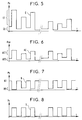
- FIG. 5 shows, by way of example and schematically, the variations as a function of time of the optical power Pe of the input signal E. It is assumed that a first data stream with high average optical power is followed by a second data stream with lower average optical power. Furthermore, the high levels E1 and low E0 of the signal E exhibit significant fluctuations.
- the fiber amplifier 3 is designed to operate in gain saturation mode. This results in an equalization of the average optical power of the amplified signal AE.
- FIG. 6 represents the variations as a function of time of the optical power Pae of the amplified signal AE.
- FIG. 2 schematically shows the variations in the gain G of the amplifier OA as a function of the total optical power P it receives.
- the power P is the sum of the power Pl of the intermediate wave L and the power Pae of the amplified signal AE.
- the curve shown corresponds to the case of a stabilized gain amplifier produced for example in accordance with the teachings of European patent application EP-A-639 876.
- Such an amplifier has the property of keeping a constant gain for a wide range of variations in the optical power it receives.
- the gain decreases sharply when the power exceeds a threshold value characteristic of the chosen amplifier.
- the power modulation of the amplified input signal AE is capable of modulating the gain G between a high constant value G0 and low values G1.
- This gain modulation applies to the auxiliary wave L whose power P1 is constant.
- the amplifier OA emits towards the circulator 5 a power-modulated wave whose high levels are practically independent of the fluctuations of the low levels of the input signal E.
- the modulating signal B obtained after a possible filtering F also exhibits this property as shown in FIG. 7.
- the second stage 2 of the device of FIG. 1 comprises an interferometric structure 7 consisting of two guiding branches provided respectively with optical semiconductor amplifiers OA1 and OA2.
- a first coupler K1 makes it possible to couple one end of each of these branches to a laser source 8 providing an output carrier wave M of wavelength ⁇ s.
- a second coupler K2 is arranged so as to allow the introduction of the modulating signal B into the first amplifier OA1.
- a third coupler K3 connected to the coupler K2 and to the second amplifier OA2 is arranged so as to provide an output signal S resulting from the coupling of auxiliary waves AM1 and AM2 supplied respectively by the amplifiers OA1 and OA2.
- the waves AM1 and AM2 correspond to the waves M1 and M2 from the coupler K1 and amplified respectively by the amplifiers OA1 and OA2.
- the current I2 can be adjusted to a value I21 greater than I20 for obtain a response from the interferometric structure 7 in accordance with FIG. 4.
- the interference is destructive when the power of signal B is low and constructive when it is high.
- the variations in the power Ps of the output signal as a function of time will be represented in accordance with FIG. 8.
- the assembly can be completed by an output filter F ' calibrated on the wavelength ⁇ s so as to eliminate the amplified spontaneous emissions produced by the amplifiers OA1 and OA2.
- the assembly which has just been presented therefore allows excellent reshaping of the input signal while tolerating large fluctuations in its high and low levels.
- the role of the first stage in particular is to stabilize the operation of the interferometric structure 7 of the second stage 2 while the latter has the role of regenerating the rate of extinction degraded by the first stage.
- a wavelength ⁇ b will advantageously be chosen which ensures maximum gain for the amplifier OA1 for the injection current I1 chosen.
- a high current I1 for example 200 mA
- the value I20 of the current I2 is sought such that the power Ps of the output signal is maximum S1.
- the power B1 of the signal B to be injected is sought so that the output power Ps is minimum S0.
- the value of the current I to inject into the amplifier OA of the clipper 4 so that the level signal B high power is equal to the previously determined value B1.
- auxiliary waves AM1 and AM2 For this, one can for example use as source 8 a laser with integrated modulator. A current Is is then injected into the laser part while a modulation voltage D is applied in reverse to the modulator part. With such a device, it is possible to erase the input data by canceling the optical power of the M wave supplied by the modulator.
- the interference is destructive when the signal B is in the high state, it will be possible to insert data when this signal B is in the low state by modulating the power of the M wave by modulation of the voltage D
- the interference is constructive when the signal B is in the high state, it will be possible to insert data when this signal is in the high state by modulating the power of the signal M as previously.
- Modifications of the input signal can also be carried out by modulating the power P1, for example by means of a modulator placed between the source 6 and the amplifier OA.
- This possibility can be advantageously used to resynchronize a synchronous input signal E, that is to say to eliminate the jitter which may affect it.
- a sampling clock signal (not shown in the figure) consisting of pulses of width less than bit time of the input signal, of frequency equal to the bit frequency and set approximately in the middle of the bit time intervals of the signal. If the pulse duration is equal to half the bit time of the input signal, an RZ type signal can be obtained at the output.
- FIG. 9 represents an alternative embodiment of the interferometric structure 7.
- the structure is also of the Mach-Zehnder type but the modulating signal B and the wave M are injected into the first amplifier OA1 according to the same direction of propagation.
- the operation is similar to that of the structure shown in FIG. 1 with the difference that an output filter F 'capable of effectively eliminating the wavelength ⁇ b is placed at the output of the device.
- FIG. 10 represents another Michelson-type structure equivalent to the previous one.
- the two amplifiers OA1 and OA2 are coupled by only one of their ends, the opposite faces being provided with a reflective coating R1, R2.
- the modulating signal is injected into the first amplifier OA1 via the face R1 and the M wave is injected into the two amplifiers OA1 and OA2 by the faces opposite to the faces R1 and R2 via a set K1 formed of a circulator associated with a coupler.
- a first port of the circulator receives the M wave, the second port is coupled to the two amplifiers OA1, OA2 and a third port supplies the output signal S.
- FIG. 11 represents an alternative embodiment of the clipper 4.
- the operating principle is analogous to that of the device represented in FIG. 1 with the difference that the L wave and the amplified input signal AE are injected into the OA amplifier with the same direction of propagation. It is then necessary to provide a rejector filter F capable of effectively eliminating the wavelength ⁇ e of the input signal.
Landscapes
- Physics & Mathematics (AREA)
- Electromagnetism (AREA)
- General Physics & Mathematics (AREA)
- Optics & Photonics (AREA)
- Computer Networks & Wireless Communication (AREA)
- Engineering & Computer Science (AREA)
- Nonlinear Science (AREA)
- Signal Processing (AREA)
- Condensed Matter Physics & Semiconductors (AREA)
- Optical Communication System (AREA)
- Lasers (AREA)
- Semiconductor Lasers (AREA)
- Optical Modulation, Optical Deflection, Nonlinear Optics, Optical Demodulation, Optical Logic Elements (AREA)
Abstract
Description
L'invention se situe dans le domaine des systèmes optoélectroniques utilisés pour la transmission ou le traitement optique de données numériques optiques.The invention relates to the field of optoelectronic systems used for the optical transmission or processing of optical digital data.
Dans ces systèmes, les informations sont souvent sous la forme de données binaires représentées par des impulsions modulant une onde porteuse optique. Une valeur binaire est donc déterminée en fonction du niveau d'amplitude (ou de puissance) de l'onde optique modulée.In these systems, the information is often in the form of binary data represented by pulses modulating an optical carrier wave. A binary value is therefore determined as a function of the amplitude (or power) level of the modulated optical wave.
Au cours de la transmission, ce signal subit inévitablement des dégradations qui rendent plus difficile au niveau des récepteurs la détection des niveaux hauts et bas du signal reçu. Dans le domaine de l'amplitude, la qualité d'un signal optique est habituellement définie par deux paramètres : le rapport signal à bruit et le taux d'extinction. Le rapport signal à bruit est défini comme le rapport de la puissance optique du signal à la puissance de bruit dans une bande de longueur d'onde contenant la longueur d'onde de la porteuse du signal. Le taux d'extinction est défini comme le rapport des puissances correspondant respectivement aux niveaux hauts et bas du signal.During transmission, this signal inevitably undergoes degradations which make it more difficult at the level of the receivers to detect the high and low levels of the received signal. In the amplitude domain, the quality of an optical signal is usually defined by two parameters: the signal to noise ratio and the extinction rate. The signal to noise ratio is defined as the ratio of the optical power of the signal to the noise power in a wavelength band containing the wavelength of the signal carrier. The extinction rate is defined as the ratio of the powers corresponding respectively to the high and low levels of the signal.
L'invention a pour but de proposer un dispositif entièrement optique, c'est-à-dire sans conversion optique-électrique et inversement, qui soit capable d'améliorer la qualité d'un signal optique binaire, c'est-à-dire d'augmenter le taux d'extinction tout en conservant un rapport signal à bruit le plus grand possible. En d'autres termes, le dispositif doit être capable à partir d'un signal d'entrée modulé de mauvaise qualité de fournir un signal de sortie dont les niveaux hauts sont stabilisés avec une puissance optique constante, dont les niveaux bas ont une puissance pratiquement nulle, tout en présentant un rapport signal à bruit très élevé.The invention aims to provide a fully optical device, that is to say without optical-electrical conversion and vice versa, which is capable of improving the quality of a binary optical signal, that is to say increase the extinction rate while maintaining the highest signal-to-noise ratio possible. In other words, the device must be able, from a modulated input signal of poor quality, to provide an output signal whose high levels are stabilized with constant optical power, whose low levels have a power practically zero, while having a very high signal-to-noise ratio.
Une solution envisageable pour augmenter le taux d'extinction consiste à utiliser une structure interférométrique, par exemple de type Mach-Zehnder. La structure se compose de deux branches véhiculant deux ondes cohérentes couplées pour former le signal de sortie. L'une des branches comporte un milieu dont l'indice varie en fonction de la puissance optique qu'elle véhicule et un signal d'entrée est introduit dans cette branche. Les variations de puissance du signal d'entrée modulent alors l'indice et les deux ondes peuvent interférer de façon destructive ou constructive en fonction du niveau de puissance du signal d'entrée.One possible solution for increasing the extinction rate consists in using an interferometric structure, for example of the Mach-Zehnder type. The structure consists of two branches carrying two coherent waves coupled to form the output signal. One of the branches has a medium, the index of which varies as a function of the optical power which it carries and an input signal is introduced into this branch. The variations in power of the input signal then modulate the index and the two waves can interfere destructively or constructively depending on the power level of the input signal.
Une telle structure permet bien d'améliorer le taux d'extinction mais présente l'inconvénient que les conditions d'interférences destructive et constructive sont très contraignantes vis-à-vis du signal d'entrée, en particulier de sa longueur d'onde et surtout de son niveau de puissance à l'état haut. Il en résulte un fonctionnement très sensible aux fluctuations de ces paramètres.Such a structure makes it possible to improve the extinction rate but has the drawback that the destructive and constructive interference conditions are very restrictive with respect to the input signal, in particular its wavelength and especially its high power level. This results in operation that is very sensitive to fluctuations in these parameters.
L'invention a pour but de remédier aux inconvénients du dispositif précédent. Dans ce but, l'invention a pour objet un dispositif de mise en forme d'un signal binaire d'entrée ayant la forme d'une première onde optique modulée entre des niveaux bas et hauts de puissance, caractérisés en ce qu'il comporte :
- un premier étage pour fournir, en fonction dudit signal d'entrée, un signal optique modulant ayant la forme d'une seconde onde optique de longueur d'onde déterminée et modulée entre des premiers et des seconds niveaux de puissance, les plus hauts parmi lesdits premiers et seconds niveaux étant stabilisés pour être peu dépendants des fluctuations desdits niveaux bas et hauts du signal d'entrée et
- un second étage comportant une structure interférométrique couplée audit premier étage pour recevoir ledit signal modulant et conçue de façon à fournir un signal de sortie résultant d'une interférence respectivement constructive ou destructive de première et seconde ondes auxiliaires lorsque la puissance du signal modulant est égale respectivement auxdits premiers ou seconds niveaux.
- a first stage for supplying, as a function of said input signal, a modulating optical signal having the form of a second optical wave of wavelength determined and modulated between first and second power levels, the highest among said first and second levels being stabilized to be less dependent fluctuations of said low and high levels of the input signal and
- a second stage comprising an interferometric structure coupled to said first stage for receiving said modulating signal and designed so as to provide an output signal resulting from respectively constructive or destructive interference from the first and second auxiliary waves when the power of the modulating signal is equal respectively at said first or second levels.
Ainsi, le premier étage a pour rôle de supprimer les fluctuations éventuelles des niveaux hauts du signal modulant introduit dans la structure interférométrique. Il en résulte un fonctionnement stable de cette structure. En outre, le dispositif est indépendant de la valeur ou des fluctuations de la longueur d'onde du signal optique d'entrée ainsi que de sa polarisation.Thus, the role of the first stage is to suppress any fluctuations in the high levels of the modulating signal introduced into the interferometric structure. This results in stable operation of this structure. In addition, the device is independent of the value or of the fluctuations of the wavelength of the optical input signal as well as of its polarization.
Selon un mode de réalisation particulier le dispositif est caractérisé en ce que ladite structure interférométrique comporte une première et une seconde branche guidante recevant par des premiers moyens de couplage respectivement une première et une seconde partie d'une troisième onde optique, lesdites branches étant munies respectivement d'un premier et d'un second amplificateur optique semi-conducteur, ledit premier amplificateur recevant par des seconds moyens de couplage ledit signal modulant, lesdits premiers et seconds amplificateurs étant alimentés par des courants électriques ajustés pour fournir respectivement lesdites première et seconde ondes auxiliaires.According to a particular embodiment, the device is characterized in that said interferometric structure comprises a first and a second guiding branch receiving by first coupling means respectively a first and a second part of a third optical wave, said branches being provided respectively a first and a second semiconductor optical amplifier, said first amplifier receiving by second coupling means said modulating signal, said first and second amplifiers being supplied by electric currents adjusted to supply said first and second auxiliary waves respectively .
Ainsi, en plus de l'effet d'amplification apporté par les amplificateurs semi-conducteurs, on exploite aussi leur propriété de posséder un indice fonction à la fois de la puissance optique totale qu'il reçoit et du courant injecté dans sa couche active. Cela permet donc d'ajuster aisément le point de fonctionnement de la structure interférométrique.Thus, in addition to the amplification effect provided by semiconductor amplifiers, we also exploit their property of having an index which is a function both of the total optical power it receives and of the current injected into its active layer. This therefore makes it possible to easily adjust the operating point of the interferometric structure.
Avantageusement, les premier et second moyens de couplage sont disposés de façon à ce que ledit premier amplificateur fournisse ladite première onde auxiliaire et reçoive ledit signal modulant selon des sens de propagation opposés.Advantageously, the first and second coupling means are arranged so that said first amplifier supplies said first auxiliary wave and receives said signal modulating in opposite directions of propagation.
Cette dernière disposition facilite l'extraction du signal de sortie.This latter arrangement facilitates the extraction of the output signal.
D'autre part, le bruit qui accompagne le signal de sortie est essentiellement dû à l'émission spontanée amplifiée ("A S E") produite par les amplificateurs semi-conducteurs de la structure interférométrique. Aussi, pour en atténuer les effets sur le signal de sortie et selon un autre aspect de l'invention, les courants sont ajustés pour que ladite interférence soit destructive lorsque lesdits premiers niveaux sont les plus hauts niveaux du signal modulant.On the other hand, the noise which accompanies the output signal is essentially due to the amplified spontaneous emission ("A S E") produced by the semiconductor amplifiers of the interferometric structure. Also, to attenuate the effects thereof on the output signal and according to another aspect of the invention, the currents are adjusted so that said interference is destructive when said first levels are the highest levels of the modulating signal.
Selon un mode de réalisation préféré, ledit premier étage comporte un troisième amplificateur semi-conducteur apte à recevoir ledit signal d'entrée ainsi qu'une quatrième onde optique. Le troisième amplificateur et/ou le signal d'entrée sont alors dimensionnés pour placer le troisième amplificateur en état de saturation de gain lorsque le signal d'entrée est à l'état haut. Enfin, le signal modulant est constitué par ladite quatrième onde optique amplifiée par ledit troisième amplificateur.According to a preferred embodiment, said first stage comprises a third semiconductor amplifier capable of receiving said input signal as well as a fourth optical wave. The third amplifier and / or the input signal are then sized to place the third amplifier in the gain saturation state when the input signal is in the high state. Finally, the modulating signal consists of said fourth optical wave amplified by said third amplifier.
Avantageusement, le troisième amplificateur est un amplificateur optique semi-conducteur à gain stabilisé. Cette dernière disposition présente l'intérêt que le niveau haut du signal modulant reste constant même si le niveau bas du signal d'entrée subit d'importantes variations. Ceci contribue à améliorer la stabilité de fonctionnement de la structure interférométrique.Advantageously, the third amplifier is a stabilized gain semiconductor optical amplifier. This latter arrangement has the advantage that the high level of the modulating signal remains constant even if the low level of the input signal is subject to significant variations. This contributes to improving the operating stability of the interferometric structure.
Le dispositif de mise en forme selon l'invention peut être avantageusement utilisé pour effectuer des modifications des données reçues. Plus précisément, il permet d'effacer une partie des données d'un signal reçu ou d'y insérer de nouvelles données. L'effacement ou l'inscription de données est par exemple utile dans les matrices de commutation qui traitent des données associées à un en-tête contenant des informations de routage.The shaping device according to the invention can advantageously be used to make modifications to the data received. More precisely, it makes it possible to erase part of the data of a received signal or to insert new data into it. Erasing or writing data is useful, for example, in switching matrices that process data associated with a header containing routing information.
Aussi l'invention a également pour objet un procédé pour modifier un signal optique binaire d'entrée, caractérisé en ce qu'il consiste à appliquer ledit signal d'entrée au dispositif de mise en forme selon l'invention et à moduler en puissance lesdites ondes auxiliaires.The invention also also relates to a method for modifying a binary optical input signal, characterized in that it consists in applying said input signal to the shaping device according to the invention and in modulating said power auxiliary waves.
En variante, l'invention prévoit en outre de modifier le signal optique binaire d'entrée en modulant en puissance ladite quatrième onde optique ou en modulant le courant électrique appliqué audit troisième amplificateur. En particulier, la modulation de la quatrième onde optique par un signal d'échantillonnage approprié permet à la fois une remise en forme et une resynchronisation d'un signal binaire d'entrée.Alternatively, the invention further provides for modifying the binary optical input signal by power modulating said fourth optical wave or by modulating the electric current applied to said third amplifier. In particular, the modulation of the fourth optical wave by an appropriate sampling signal allows both reshaping and resynchronization of an input binary signal.
D'autres aspects et avantages de l'invention apparaîtront dans la suite de la description en référence aux figures.
- La figure 1 représente schématiquement un mode de réalisation préféré du dispositif selon l'invention.
- Les figures 2 à 4 sont des courbes permettant d'expliquer le principe de fonctionnement du dispositif de la figure 1.
- Les figures 5 à 8 sont des chronogrammes montrant des transformations de signaux optiques binaires effectuées par le dispositif selon l'invention.
- Les figures 9 et 10 sont des variantes de réalisation de la structure interférométrique faisant partie du dispositif selon l'invention.
- La figure 11 est une variante de réalisation du premier étage du dispositif selon l'invention.
- FIG. 1 schematically represents a preferred embodiment of the device according to the invention.
- FIGS. 2 to 4 are curves making it possible to explain the operating principle of the device of FIG. 1.
- Figures 5 to 8 are timing diagrams showing transformations of binary optical signals performed by the device according to the invention.
- Figures 9 and 10 are alternative embodiments of the interferometric structure forming part of the device according to the invention.
- Figure 11 is an alternative embodiment of the first stage of the device according to the invention.
Le dispositif représenté à la figure 1 comprend un premier étage 1 recevant un signal optique binaire d'entrée E destiné à être mis en forme par le dispositif et fournissant à un second étage 2 un signal optique modulant B.The device represented in FIG. 1 comprises a
Le premier étage 1 comporte un amplificateur optique à fibres 3 recevant le signal d'entrée E et fournissant un signal d'entrée amplifié AE à un dispositif écrêteur 4. Le dispositif écrêteur 4 comporte un amplificateur optique semi-conducteur OA dont une première face est couplée à un oscillateur laser 6 fournissant une onde porteuse intermédiaire L. L'autre face de l'amplificateur OA est reliée à un circulateur 5 comportant un premier et un second ports prévus respectivement pour recevoir de l'amplificateur à fibres 3 le signal d'entrée amplifié AE et l'injecter dans l'amplificateur OA. Un troisième port du circulateur 5 fournit le signal modulant B par l'intermédiaire d'un filtre réjecteur F calé sur la longueur d'onde λe du signal d'entrée E. La longueur d'onde λb de l'onde intermédiaire L est choisie différente de celle du signal d'entrée E et sera avantageusement modifiable en utilisant comme source 6 un oscillateur laser accordable en longueur d'onde.The
Le fonctionnement du premier étage peut être expliqué à l'aide des figures 2, 5, 6 et 7. La figure 5 représente, à titre d'exemple et de façon schématique, les variations en fonction du temps de la puissance optique Pe du signal d'entrée E. Il est supposé qu'un premier train de données à forte puissance optique moyenne est suivi d'un second train de données à puissance optique moyenne plus faible. Par ailleurs, les niveaux hauts E1 et bas E0 du signal E présentent des fluctuations importantes. L'amplificateur à fibres 3 est prévu pour fonctionner en mode de saturation de gain. Il en résulte une égalisation de la puissance optique moyenne du signal amplifié AE. La figure 6 représente les variations en fonction du temps de la puissance optique Pae du signal amplifié AE.The operation of the first stage can be explained using FIGS. 2, 5, 6 and 7. FIG. 5 shows, by way of example and schematically, the variations as a function of time of the optical power Pe of the input signal E. It is assumed that a first data stream with high average optical power is followed by a second data stream with lower average optical power. Furthermore, the high levels E1 and low E0 of the signal E exhibit significant fluctuations. The fiber amplifier 3 is designed to operate in gain saturation mode. This results in an equalization of the average optical power of the amplified signal AE. FIG. 6 represents the variations as a function of time of the optical power Pae of the amplified signal AE.
La figure 2 montre schématiquement les variations du gain G de l'amplificateur OA en fonction de la puissance optique totale P qu'il reçoit. Dans le cas de l'écrêteur 4, la puissance P est la somme de la puissance Pl de l'onde intermédiaire L et de la puissance Pae du signal amplifié AE. La courbe représentée correspond au cas d'un amplificateur à gain stabilisé réalisé par exemple conformément aux enseignements de la demande de brevet européen EP-A-639 876. Un tel amplificateur a la propriété de conserver un gain constant pour une large plage de variations de la puissance optique qu'il reçoit. Par contre, le gain diminue fortement lorsque la puissance dépasse une valeur de seuil caractéristique de l'amplificateur choisi. Grâce à un dimensionnement approprié de l'amplificateur à fibres 3 et/ou de l'amplificateur semi-conducteur OA, la modulation de puissance du signal d'entrée amplifié AE est capable de moduler le gain G entre une valeur haute constante G0 et des valeurs faibles G1. Cette modulation de gain s'applique à l'onde auxiliaire L dont la puissance Pl est constante. Il en résulte que l'amplificateur OA émet en direction du circulateur 5 une onde modulée en puissance dont les niveaux hauts sont pratiquement indépendants des fluctuations des niveaux bas du signal d'entrée E. Ainsi, le signal modulant B obtenu après un éventuel filtrage F présente également cette propriété comme représenté à la figure 7.FIG. 2 schematically shows the variations in the gain G of the amplifier OA as a function of the total optical power P it receives. In the case of the clipper 4, the power P is the sum of the power Pl of the intermediate wave L and the power Pae of the amplified signal AE. The curve shown corresponds to the case of a stabilized gain amplifier produced for example in accordance with the teachings of European patent application EP-A-639 876. Such an amplifier has the property of keeping a constant gain for a wide range of variations in the optical power it receives. On the other hand, the gain decreases sharply when the power exceeds a threshold value characteristic of the chosen amplifier. Thanks to an appropriate dimensioning of the fiber amplifier 3 and / or of the semiconductor amplifier OA, the power modulation of the amplified input signal AE is capable of modulating the gain G between a high constant value G0 and low values G1. This gain modulation applies to the auxiliary wave L whose power P1 is constant. As a result, the amplifier OA emits towards the circulator 5 a power-modulated wave whose high levels are practically independent of the fluctuations of the low levels of the input signal E. Thus, the modulating signal B obtained after a possible filtering F also exhibits this property as shown in FIG. 7.
Le second étage 2 du dispositif de la figure 1 comporte une structure interférométrique 7 constituée de deux branches guidantes munies respectivement d'amplificateurs optiques semi-conducteurs OA1 et OA2. Un premier coupleur K1 permet de coupler une extrémité de chacune de ces branches à une source laser 8 fournissant une onde porteuse de sortie M de longueur d'onde λs. Un second coupleur K2 est disposé de façon à permettre l'introduction du signal modulant B dans le premier amplificateur OA1. Un troisième coupleur K3 relié au coupleur K2 et au second amplificateur OA2 est disposé de façon à fournir un signal de sortie S résultant du couplage d'ondes auxiliaires AM1 et AM2 fournies respectivement par les amplificateurs OA1 et OA2. Les ondes AM1 et AM2 correspondent aux ondes M1 et M2 issues du coupleur K1 et amplifiées respectivement par les amplificateurs OA1 et OA2.The second stage 2 of the device of FIG. 1 comprises an interferometric structure 7 consisting of two guiding branches provided respectively with optical semiconductor amplifiers OA1 and OA2. A first coupler K1 makes it possible to couple one end of each of these branches to a laser source 8 providing an output carrier wave M of wavelength λs. A second coupler K2 is arranged so as to allow the introduction of the modulating signal B into the first amplifier OA1. A third coupler K3 connected to the coupler K2 and to the second amplifier OA2 is arranged so as to provide an output signal S resulting from the coupling of auxiliary waves AM1 and AM2 supplied respectively by the amplifiers OA1 and OA2. The waves AM1 and AM2 correspond to the waves M1 and M2 from the coupler K1 and amplified respectively by the amplifiers OA1 and OA2.
Des courants I1 et I2 sont injectés respectivement dans les amplificateurs OA1 et OA2. Selon une première possibilité, ces courants sont ajustés de façon à ce que le signal de sortie S résulte d'une interférence constructive des ondes AM1 et AM2 lorsque la puissance du signal modulant B est basse et résulte d'une interférence destructive dans le cas contraire. Ce cas est illustré à la figure 3 qui représente la puissance de sortie Ps du signal S en fonction de la puissance Pb du signal modulant B lorsque le courant I2 a la valeur I20.Currents I1 and I2 are injected respectively into the amplifiers OA1 and OA2. According to a first possibility, these currents are adjusted so that the output signal S results from a constructive interference of the waves AM1 and AM2 when the power of the modulating signal B is low and results from a destructive interference otherwise . This case is illustrated in FIG. 3 which represents the output power Ps of the signal S as a function of the power Pb of the modulating signal B when the current I2 has the value I20.
Selon une autre possibilité, le courant I2 peut être ajustés à une valeur I21 supérieure à I20 pour obtenir une réponse de la structure interférométrique 7 conformément à la figure 4. Dans ce cas, l'interférence est destructive lorsque la puissance du signal B est faible et constructive lorsqu'elle est élevée.According to another possibility, the current I2 can be adjusted to a value I21 greater than I20 for obtain a response from the interferometric structure 7 in accordance with FIG. 4. In this case, the interference is destructive when the power of signal B is low and constructive when it is high.
Ainsi, dans le cas d'une réponse conforme à la figure 3, les variations de la puissance Ps du signal de sortie en fonction du temps seront représentées conformément à la figure 8. L'ensemble peut être complété par un filtre de sortie F' calé sur la longueur d'onde λs de façon à éliminer les émissions spontanées amplifiées produites par les amplificateurs OA1 et OA2.Thus, in the case of a response in accordance with FIG. 3, the variations in the power Ps of the output signal as a function of time will be represented in accordance with FIG. 8. The assembly can be completed by an output filter F ' calibrated on the wavelength λs so as to eliminate the amplified spontaneous emissions produced by the amplifiers OA1 and OA2.
L'ensemble qui vient d'être présenté permet donc une excellente remise en forme du signal d'entrée en tolérant de fortes fluctuations de ses niveaux hauts et bas. Le premier étage a notamment pour rôle de stabiliser le fonctionnement de la structure interférométrique 7 du second étage 2 tandis que ce dernier a pour rôle de régénérer le taux d'extinction dégradé par le premier étage.The assembly which has just been presented therefore allows excellent reshaping of the input signal while tolerating large fluctuations in its high and low levels. The role of the first stage in particular is to stabilize the operation of the interferometric structure 7 of the second stage 2 while the latter has the role of regenerating the rate of extinction degraded by the first stage.
Dans le cas où la source 6 est accordable en longueur d'onde, on choisira avantageusement une longueur d'onde λb qui assure un gain maximal à l'amplificateur OA1 pour le courant d'injection I1 choisi.In the case where the source 6 is tunable in wavelength, a wavelength λb will advantageously be chosen which ensures maximum gain for the amplifier OA1 for the injection current I1 chosen.
Concernant le choix des courants I1 et I2 dans le cas par exemple de la réponse selon la figure 3, on peut utiliser la méthode suivante. On applique un courant I1 élevé, par exemple de 200 mA, avec un signal B de puissance nulle et on cherche la valeur I20 du courant I2 telle que la puissance Ps du signal de sortie soit maximale S1. Ensuite, en conservant les mêmes courants, on recherche la puissance B1 du signal B à injecter pour que la puissance de sortie Ps soit minimale S0. On cherche enfin la valeur du courant I à injecter dans l'amplificateur OA de l'écrêteur 4 pour que le niveau haut de puissance du signal B soit égal à la valeur B1 précédemment déterminée.Concerning the choice of the currents I1 and I2 in the case for example of the response according to FIG. 3, the following method can be used. A high current I1, for example 200 mA, is applied with a signal B of zero power and the value I20 of the current I2 is sought such that the power Ps of the output signal is maximum S1. Then, keeping the same currents, the power B1 of the signal B to be injected is sought so that the output power Ps is minimum S0. Finally, we look for the value of the current I to inject into the amplifier OA of the clipper 4 so that the level signal B high power is equal to the previously determined value B1.
Pour effectuer des modifications du signal d'entrée en utilisant le dispositif qui vient d'être décrit, il convient de prévoir des moyens permettant de moduler la puissance des ondes auxiliaires AM1 et AM2. Pour cela, on peut par exemple utiliser comme source 8 un laser à modulateur intégré. Un courant Is est alors injecté dans la partie laser tandis qu'une tension de modulation D est appliquée en inverse sur la partie modulateur. Avec un tel dispositif, il est possible d'effacer les données d'entrée en annulant la puissance optique de l'onde M fournie par la modulateur. Dans le cas où l'interférence est destructive lorsque le signal B est à l'état haut, on pourra insérer des données lorsque ce signal B est à l'état bas en modulant la puissance de l'onde M par modulation de la tension D. Dans le cas où l'interférence est constructive lorsque le signal B est à l'état haut, on pourra insérer des données lorsque ce signal est à l'état haut en modulant la puissance du signal M comme précédemment.To make changes to the input signal using the device which has just been described, it is necessary to provide means making it possible to modulate the power of the auxiliary waves AM1 and AM2. For this, one can for example use as source 8 a laser with integrated modulator. A current Is is then injected into the laser part while a modulation voltage D is applied in reverse to the modulator part. With such a device, it is possible to erase the input data by canceling the optical power of the M wave supplied by the modulator. In the case where the interference is destructive when the signal B is in the high state, it will be possible to insert data when this signal B is in the low state by modulating the power of the M wave by modulation of the voltage D In the case where the interference is constructive when the signal B is in the high state, it will be possible to insert data when this signal is in the high state by modulating the power of the signal M as previously.
Des modifications du signal d'entrée peuvent aussi être effectuées en modulant la puissance Pl, par exemple au moyen d'un modulateur placé entre la source 6 et l'amplificateur OA. Cette possibilité peut être avantageusement utilisée pour resynchroniser un signal d'entrée E synchrone, c'est-à-dire supprimer la gigue pouvant l'affecter. Par exemple, dans le cas d'un signal d'entrée de type NRZ, il suffit pour cela de moduler la puissance P1 par un signal d'horloge d'échantillonnage (non représenté sur la figure) constitué d'impulsions de largeur inférieure au temps bit du signal d'entrée, de fréquence égale à la fréquence bit et calées environ au milieu des intervalles de temps bit du signal. Si la durée des impulsions est égale à la moitié du temps bit du signal d'entrée, on peut obtenir en sortie un signal de type RZ.Modifications of the input signal can also be carried out by modulating the power P1, for example by means of a modulator placed between the source 6 and the amplifier OA. This possibility can be advantageously used to resynchronize a synchronous input signal E, that is to say to eliminate the jitter which may affect it. For example, in the case of an NRZ type input signal, it suffices to modulate the power P1 by a sampling clock signal (not shown in the figure) consisting of pulses of width less than bit time of the input signal, of frequency equal to the bit frequency and set approximately in the middle of the bit time intervals of the signal. If the pulse duration is equal to half the bit time of the input signal, an RZ type signal can be obtained at the output.
Si par contre on veut fournir un signal de sortie S de type NRZ, on peut simplement ajuster les courants I1 et I2 de façon à ce que la bande passante de l'amplificateur OA1, donc du second étage 2, présente une fréquence de coupure comprise entre la fréquence bit et la moitié de cette fréquence.If on the other hand one wants to provide an output signal S of NRZ type, one can simply adjust the currents I1 and I2 so that the passband of the amplifier OA1, therefore of the second stage 2, has a cut-off frequency included between the bit frequency and half of that frequency.
On peut également procéder à des effacements partiels du signal en modulant le courant I qui alimente l'amplificateur OA.It is also possible to carry out partial erasures of the signal by modulating the current I which supplies the amplifier OA.
La figure 9 représente une variante de réalisation de la structure interférométrique 7. la structure est aussi de type Mach-Zehnder mais le signal modulant B et l'onde M sont injectés dans le premier amplificateur OA1 selon le même sens de propagation. Le fonctionnement est analogue à celui de la structure représentée à la figure 1 à la différence près qu'un filtre de sortie F' capable d'éliminer efficacement la longueur d'onde λb soit placé en sortie du dispositif.FIG. 9 represents an alternative embodiment of the interferometric structure 7. the structure is also of the Mach-Zehnder type but the modulating signal B and the wave M are injected into the first amplifier OA1 according to the same direction of propagation. The operation is similar to that of the structure shown in FIG. 1 with the difference that an output filter F 'capable of effectively eliminating the wavelength λb is placed at the output of the device.
La figure 10 représente une autre structure de type Michelson équivalente à la précédente. Selon cette variante, les deux amplificateurs OA1 et OA2 sont couplés par une seule de leurs extrémités, les faces opposées étant munies d'un revêtement réfléchissant R1, R2. Le signal modulant est injecté dans le premier amplificateur OA1 par l'intermédiaire de la face R1 et l'onde M est injectée dans les deux amplificateurs OA1 et OA2 par les faces opposées aux faces R1 et R2 par l'intermédiaire d'un ensemble K1 formé d'un circulateur associé à un coupleur. Un premier port du circulateur reçoit l'onde M, le second port est couplé aux deux amplificateurs OA1, OA2 et un troisième port fournit le signal de sortie S.FIG. 10 represents another Michelson-type structure equivalent to the previous one. According to this variant, the two amplifiers OA1 and OA2 are coupled by only one of their ends, the opposite faces being provided with a reflective coating R1, R2. The modulating signal is injected into the first amplifier OA1 via the face R1 and the M wave is injected into the two amplifiers OA1 and OA2 by the faces opposite to the faces R1 and R2 via a set K1 formed of a circulator associated with a coupler. A first port of the circulator receives the M wave, the second port is coupled to the two amplifiers OA1, OA2 and a third port supplies the output signal S.
La figure 11 représente une variante de réalisation de l'écrêteur 4. Le principe de fonctionnement est analogue à celui du dispositif représenté à la figure 1 à la différence près que l'onde L et le signal d'entrée amplifié AE sont injectés dans l'amplificateur OA avec le même sens de propagation. Il est alors nécessaire de prévoir un filtre réjecteur F capable d'éliminer efficacement la longueur d'onde λe du signal d'entrée.FIG. 11 represents an alternative embodiment of the clipper 4. The operating principle is analogous to that of the device represented in FIG. 1 with the difference that the L wave and the amplified input signal AE are injected into the OA amplifier with the same direction of propagation. It is then necessary to provide a rejector filter F capable of effectively eliminating the wavelength λe of the input signal.
On peut noter que dans la réalisation de l'écrêteur 4 de la figure 1, il est possible de supprimer le filtre F en prévoyant des traitements antireflet sur les faces de l'amplificateur OA. Dans ce cas, il sera facile d'intégrer dans un même composant les trois amplificateurs OA, OA1, OA2, à condition toutefois de remplacer le circulateur 5 par un simple coupleur.It can be noted that in the embodiment of the clipper 4 of FIG. 1, it is possible to remove the filter F by providing anti-reflective treatments on the faces of the amplifier OA. In this case, it will be easy to integrate the three amplifiers OA, OA1, OA2 into the same component, provided however that the
Claims (14)
Applications Claiming Priority (2)
| Application Number | Priority Date | Filing Date | Title |
|---|---|---|---|
| FR9607421 | 1996-06-14 | ||
| FR9607421A FR2749946B1 (en) | 1996-06-14 | 1996-06-14 | DEVICE FOR SHAPING BINARY OPTICAL SIGNALS AND ITS USE FOR MODIFYING SAID SIGNALS |
Publications (2)
| Publication Number | Publication Date |
|---|---|
| EP0813097A1 true EP0813097A1 (en) | 1997-12-17 |
| EP0813097B1 EP0813097B1 (en) | 2006-03-01 |
Family
ID=9493062
Family Applications (1)
| Application Number | Title | Priority Date | Filing Date |
|---|---|---|---|
| EP97401290A Expired - Lifetime EP0813097B1 (en) | 1996-06-14 | 1997-06-09 | Digital optical signal regeneration device and its use for modifying digital optical signals |
Country Status (7)
| Country | Link |
|---|---|
| US (1) | US5781326A (en) |
| EP (1) | EP0813097B1 (en) |
| JP (1) | JP3563563B2 (en) |
| AT (1) | ATE319120T1 (en) |
| CA (1) | CA2208876A1 (en) |
| DE (1) | DE69735345D1 (en) |
| FR (1) | FR2749946B1 (en) |
Cited By (4)
| Publication number | Priority date | Publication date | Assignee | Title |
|---|---|---|---|---|
| GB2330967A (en) * | 1997-10-31 | 1999-05-05 | Northern Telecom Ltd | Interferometer incorporating a Kerr effect element |
| GB2335102A (en) * | 1997-05-19 | 1999-09-08 | Northern Telecom Ltd | Optical logic devices and methods |
| EP0953866A1 (en) * | 1998-04-30 | 1999-11-03 | Alcatel | Digital optical signal shaping device |
| US7057785B2 (en) | 2002-06-28 | 2006-06-06 | Corning Incorporated | Optical regenerator |
Families Citing this family (19)
| Publication number | Priority date | Publication date | Assignee | Title |
|---|---|---|---|---|
| GB2320634A (en) * | 1996-12-19 | 1998-06-24 | Northern Telecom Ltd | Optical sampling by using an interferometer to modulate a pulse train |
| US6226090B1 (en) * | 1997-07-30 | 2001-05-01 | Nec Corporation | Light timing pulses generating method and light timing circuit |
| FR2773024A1 (en) * | 1997-12-23 | 1999-06-25 | Philips Electronics Nv | SELECTIVE WRITER |
| FR2774832B1 (en) * | 1998-02-12 | 2000-08-04 | Alsthom Cge Alcatel | METHOD AND DEVICE FOR RESYNCHRONIZING OPTICAL SIGNALS |
| JP3438770B2 (en) * | 1998-03-06 | 2003-08-18 | Kddi株式会社 | Optical digital playback device |
| JP2000241778A (en) * | 1999-02-19 | 2000-09-08 | Fujitsu Ltd | Optical communication device and optical branching/ inserting device |
| EP1218988A4 (en) * | 1999-09-28 | 2005-11-23 | Univ California | Integrated wavelength tunable single and two-stage all-optical wavelength converter |
| FR2803698B1 (en) * | 2000-01-12 | 2003-06-27 | Cit Alcatel | 3R REGENERATION OF AN OPTICAL SIGNAL |
| US6563621B2 (en) * | 2000-10-06 | 2003-05-13 | Alphion Corporation | Bit-rate and format insensitive all-optical clock extraction circuit |
| US6570697B2 (en) * | 2000-10-06 | 2003-05-27 | Alphion Corporation | Format insensitive and bit rate independent optical preprocessor |
| EP1248390A1 (en) * | 2000-11-20 | 2002-10-09 | Alcatel | Optical power equalization using a gain clamped semiconductor optical amplifier |
| AU2002215757A1 (en) * | 2000-12-13 | 2002-06-24 | Bti Photonics Inc. | Optical amplifier having an improved noise figure and noise reduction method |
| US6724484B2 (en) * | 2001-05-04 | 2004-04-20 | Alphion Corporation | Format insensitive and bit rate independent optical preprocessor |
| JP4540886B2 (en) * | 2001-06-29 | 2010-09-08 | 富士通株式会社 | Method and apparatus for shaping waveform of optical signal |
| US20040208586A1 (en) * | 2002-03-27 | 2004-10-21 | Susumu Kinoshita | System and method for amplifying signals in an optical network |
| US7142788B2 (en) * | 2002-04-16 | 2006-11-28 | Corvis Corporation | Optical communications systems, devices, and methods |
| US7010234B2 (en) * | 2002-07-29 | 2006-03-07 | Alcatel Optronics Usa, Inc. | All-optical regenerator for retiming, reshaping and retransmitting an optical signal |
| US7590358B2 (en) * | 2005-02-28 | 2009-09-15 | Vladimir Grigoryan | Optical regenerative amplifier for binary phase shift-keying signals |
| CN101458369B (en) * | 2007-12-12 | 2010-08-11 | 中国科学院半导体研究所 | Monolithic integration Y wave guide connected two-laser optoelectronic device |
Citations (1)
| Publication number | Priority date | Publication date | Assignee | Title |
|---|---|---|---|---|
| US5264960A (en) * | 1992-05-08 | 1993-11-23 | At&T Bell Laboratories | Optical wavelength shifter |
Family Cites Families (4)
| Publication number | Priority date | Publication date | Assignee | Title |
|---|---|---|---|---|
| JP3123670B2 (en) * | 1991-11-11 | 2001-01-15 | キヤノン株式会社 | Semiconductor optical amplifying device and use thereof |
| US5369520A (en) * | 1992-05-22 | 1994-11-29 | At&T Corp. | Optical regeneration circuit |
| RU2099762C1 (en) * | 1992-07-06 | 1997-12-20 | Фирма "Самсунг Электроникс Ко., Лтд." | Optical regenerator |
| FR2706710B1 (en) * | 1993-06-18 | 1995-09-08 | Devaux Fabrice | Device for reshaping an optical pulse train and device for recovering a synchronized periodic signal on a modulated optical pulse train. |
-
1996
- 1996-06-14 FR FR9607421A patent/FR2749946B1/en not_active Expired - Fee Related
-
1997
- 1997-06-09 EP EP97401290A patent/EP0813097B1/en not_active Expired - Lifetime
- 1997-06-09 AT AT97401290T patent/ATE319120T1/en not_active IP Right Cessation
- 1997-06-09 DE DE69735345T patent/DE69735345D1/en not_active Expired - Lifetime
- 1997-06-13 JP JP15656797A patent/JP3563563B2/en not_active Expired - Fee Related
- 1997-06-13 US US08/874,580 patent/US5781326A/en not_active Expired - Fee Related
- 1997-06-13 CA CA002208876A patent/CA2208876A1/en not_active Abandoned
Patent Citations (1)
| Publication number | Priority date | Publication date | Assignee | Title |
|---|---|---|---|---|
| US5264960A (en) * | 1992-05-08 | 1993-11-23 | At&T Bell Laboratories | Optical wavelength shifter |
Non-Patent Citations (2)
| Title |
|---|
| JOERGENSEN C ET AL: "Wavelength conversion by optimized monolithic integrated Mach-Zehnder interferometer", IEEE PHOTONICS TECHNOLOGY LETTERS, APRIL 1996, IEEE, USA, vol. 8, no. 4, ISSN 1041-1135, pages 521 - 523, XP000587013 * |
| MIKKELSEN B ET AL: "Polarisation insensitive wavelength conversion of 10 Gbit/s signals with SOAs in a Michelson interferometer", ELECTRONICS LETTERS, 3 FEB. 1994, UK, vol. 30, no. 3, ISSN 0013-5194, pages 260 - 261, XP000431304 * |
Cited By (8)
| Publication number | Priority date | Publication date | Assignee | Title |
|---|---|---|---|---|
| GB2335102A (en) * | 1997-05-19 | 1999-09-08 | Northern Telecom Ltd | Optical logic devices and methods |
| US5999283A (en) * | 1997-05-19 | 1999-12-07 | Roberts; Kim Byron | Optical logic devices and methods |
| GB2330967A (en) * | 1997-10-31 | 1999-05-05 | Northern Telecom Ltd | Interferometer incorporating a Kerr effect element |
| US5970185A (en) * | 1997-10-31 | 1999-10-19 | Northern Telecom Limited | Optical switches, modulators and transmitters |
| EP0953866A1 (en) * | 1998-04-30 | 1999-11-03 | Alcatel | Digital optical signal shaping device |
| FR2778250A1 (en) * | 1998-04-30 | 1999-11-05 | Alsthom Cge Alcatel | DEVICE FOR SHAPING BINARY OPTICAL SIGNALS |
| US6335813B1 (en) | 1998-04-30 | 2002-01-01 | Alcatel | Device for formatting binary optical signals |
| US7057785B2 (en) | 2002-06-28 | 2006-06-06 | Corning Incorporated | Optical regenerator |
Also Published As
| Publication number | Publication date |
|---|---|
| ATE319120T1 (en) | 2006-03-15 |
| EP0813097B1 (en) | 2006-03-01 |
| FR2749946A1 (en) | 1997-12-19 |
| JP3563563B2 (en) | 2004-09-08 |
| JPH1062730A (en) | 1998-03-06 |
| DE69735345D1 (en) | 2006-04-27 |
| CA2208876A1 (en) | 1997-12-14 |
| US5781326A (en) | 1998-07-14 |
| FR2749946B1 (en) | 1998-07-31 |
Similar Documents
| Publication | Publication Date | Title |
|---|---|---|
| EP0813097B1 (en) | Digital optical signal regeneration device and its use for modifying digital optical signals | |
| EP0975107B1 (en) | Transmitting device for optical data | |
| CA2220603C (en) | Optical data transmitting device | |
| FR2751095A1 (en) | DEVICE FOR CONTROLLING LIGHT PULSES BY AN ACOUSTO-OPTIC PROGRAMMABLE DEVICE | |
| CA1311820C (en) | High frequency modulated semiconductor laser source | |
| FR2933207A1 (en) | OPTICAL MODULATION DEVICE AND OPTICAL SEMICONDUCTOR DEVICE. | |
| FR2759790A1 (en) | WAVELENGTH CONVERTER OF BINARY OPTICAL SIGNALS | |
| CA2238923C (en) | Optical transmission system with dynamic compensation of transmitted power | |
| FR2810750A1 (en) | Programmable acousto-optic filter includes birefringent material in which optical signals couple with acoustic wave pattern | |
| FR2768231A1 (en) | INTEGRATED INTERFEROMETRIC STRUCTURE | |
| EP0953866A1 (en) | Digital optical signal shaping device | |
| EP0999622A1 (en) | Optical semiconductor amplifier with adjustable stabilised gain and optical system using the same | |
| FR2758669A1 (en) | SEMICONDUCTOR OPTICAL MODULATION AND MODULATOR METHOD | |
| FR2787593A1 (en) | MACH-ZEHNDER MODULATOR WITH A VERY HIGH EXTINCTION RATE | |
| EP1134859B1 (en) | Optical amplifying device | |
| EP0746070B1 (en) | Method and device to combine optical signals | |
| FR2762104A1 (en) | METHOD AND DEVICE FOR FORMING A BINARY SIGNAL | |
| EP0795778A1 (en) | Nonlinear optical signal processing device | |
| EP0975106A1 (en) | Device for on-line regeneration of an optical soliton signal by synchronous modulation of these solitons and transmission system comprising such a device | |
| FR2739507A1 (en) | ONLINE MODULATION DEVICE FOR OPTICAL TRANSMISSION SYSTEM | |
| EP1314267A1 (en) | All-optical regenerator for wavelength-division multiplexed signals | |
| EP1311079A1 (en) | Phase controlled optical signal transmission system | |
| FR2751094A1 (en) | Acousto-optical device for programming sequence of light pulses of laser | |
| FR2879053A1 (en) | Optical signal regenerator device for e.g. dense wavelength division multiplexing network, has modulator with surface processed in antireflecting manner to limit interactions between converted signal and pumping signal parasitic reflection |
Legal Events
| Date | Code | Title | Description |
|---|---|---|---|
| PUAI | Public reference made under article 153(3) epc to a published international application that has entered the european phase |
Free format text: ORIGINAL CODE: 0009012 |
|
| AK | Designated contracting states |
Kind code of ref document: A1 Designated state(s): AT BE CH DE ES FR GB IT LI NL SE |
|
| 17P | Request for examination filed |
Effective date: 19980605 |
|
| AKX | Designation fees paid |
Free format text: AT BE CH DE ES FR GB IT LI NL SE |
|
| RBV | Designated contracting states (corrected) |
Designated state(s): AT BE CH DE ES FR GB IT LI NL SE |
|
| RAP3 | Party data changed (applicant data changed or rights of an application transferred) |
Owner name: ALCATEL |
|
| GRAP | Despatch of communication of intention to grant a patent |
Free format text: ORIGINAL CODE: EPIDOSNIGR1 |
|
| RIC1 | Information provided on ipc code assigned before grant |
Ipc: 7H 01S 5/50 B Ipc: 7H 04B 10/17 B Ipc: 7G 02F 2/00 A |
|
| RTI1 | Title (correction) |
Free format text: DIGITAL OPTICAL SIGNAL REGENERATION DEVICE AND ITS USE FOR MODIFYING DIGITAL OPTICAL SIGNALS |
|
| GRAS | Grant fee paid |
Free format text: ORIGINAL CODE: EPIDOSNIGR3 |
|
| GRAA | (expected) grant |
Free format text: ORIGINAL CODE: 0009210 |
|
| AK | Designated contracting states |
Kind code of ref document: B1 Designated state(s): AT BE CH DE ES FR GB IT LI NL SE |
|
| PG25 | Lapsed in a contracting state [announced via postgrant information from national office to epo] |
Ref country code: NL Free format text: LAPSE BECAUSE OF FAILURE TO SUBMIT A TRANSLATION OF THE DESCRIPTION OR TO PAY THE FEE WITHIN THE PRESCRIBED TIME-LIMIT Effective date: 20060301 Ref country code: IT Free format text: LAPSE BECAUSE OF FAILURE TO SUBMIT A TRANSLATION OF THE DESCRIPTION OR TO PAY THE FEE WITHIN THE PRESCRIBED TIME-LIMIT;WARNING: LAPSES OF ITALIAN PATENTS WITH EFFECTIVE DATE BEFORE 2007 MAY HAVE OCCURRED AT ANY TIME BEFORE 2007. THE CORRECT EFFECTIVE DATE MAY BE DIFFERENT FROM THE ONE RECORDED. Effective date: 20060301 Ref country code: GB Free format text: LAPSE BECAUSE OF FAILURE TO SUBMIT A TRANSLATION OF THE DESCRIPTION OR TO PAY THE FEE WITHIN THE PRESCRIBED TIME-LIMIT Effective date: 20060301 Ref country code: AT Free format text: LAPSE BECAUSE OF FAILURE TO SUBMIT A TRANSLATION OF THE DESCRIPTION OR TO PAY THE FEE WITHIN THE PRESCRIBED TIME-LIMIT Effective date: 20060301 |
|
| REG | Reference to a national code |
Ref country code: GB Ref legal event code: FG4D Free format text: NOT ENGLISH |
|
| REG | Reference to a national code |
Ref country code: CH Ref legal event code: EP |
|
| REF | Corresponds to: |
Ref document number: 69735345 Country of ref document: DE Date of ref document: 20060427 Kind code of ref document: P |
|
| PG25 | Lapsed in a contracting state [announced via postgrant information from national office to epo] |
Ref country code: SE Free format text: LAPSE BECAUSE OF FAILURE TO SUBMIT A TRANSLATION OF THE DESCRIPTION OR TO PAY THE FEE WITHIN THE PRESCRIBED TIME-LIMIT Effective date: 20060601 |
|
| PG25 | Lapsed in a contracting state [announced via postgrant information from national office to epo] |
Ref country code: DE Free format text: LAPSE BECAUSE OF FAILURE TO SUBMIT A TRANSLATION OF THE DESCRIPTION OR TO PAY THE FEE WITHIN THE PRESCRIBED TIME-LIMIT Effective date: 20060602 |
|
| PG25 | Lapsed in a contracting state [announced via postgrant information from national office to epo] |
Ref country code: ES Free format text: LAPSE BECAUSE OF FAILURE TO SUBMIT A TRANSLATION OF THE DESCRIPTION OR TO PAY THE FEE WITHIN THE PRESCRIBED TIME-LIMIT Effective date: 20060612 |
|
| PG25 | Lapsed in a contracting state [announced via postgrant information from national office to epo] |
Ref country code: LI Free format text: LAPSE BECAUSE OF NON-PAYMENT OF DUE FEES Effective date: 20060630 Ref country code: CH Free format text: LAPSE BECAUSE OF NON-PAYMENT OF DUE FEES Effective date: 20060630 Ref country code: BE Free format text: LAPSE BECAUSE OF NON-PAYMENT OF DUE FEES Effective date: 20060630 |
|
| NLV1 | Nl: lapsed or annulled due to failure to fulfill the requirements of art. 29p and 29m of the patents act | ||
| GBV | Gb: ep patent (uk) treated as always having been void in accordance with gb section 77(7)/1977 [no translation filed] |
Effective date: 20060301 |
|
| PLBE | No opposition filed within time limit |
Free format text: ORIGINAL CODE: 0009261 |
|
| STAA | Information on the status of an ep patent application or granted ep patent |
Free format text: STATUS: NO OPPOSITION FILED WITHIN TIME LIMIT |
|
| 26N | No opposition filed |
Effective date: 20061204 |
|
| REG | Reference to a national code |
Ref country code: CH Ref legal event code: PL |
|
| REG | Reference to a national code |
Ref country code: FR Ref legal event code: ST Effective date: 20070228 |
|
| BERE | Be: lapsed |
Owner name: ALCATEL Effective date: 20060630 |
|
| PG25 | Lapsed in a contracting state [announced via postgrant information from national office to epo] |
Ref country code: FR Free format text: LAPSE BECAUSE OF NON-PAYMENT OF DUE FEES Effective date: 20060630 |