EP0810608B1 - Shared bootstrap circuit - Google Patents
Shared bootstrap circuit Download PDFInfo
- Publication number
- EP0810608B1 EP0810608B1 EP97108266A EP97108266A EP0810608B1 EP 0810608 B1 EP0810608 B1 EP 0810608B1 EP 97108266 A EP97108266 A EP 97108266A EP 97108266 A EP97108266 A EP 97108266A EP 0810608 B1 EP0810608 B1 EP 0810608B1
- Authority
- EP
- European Patent Office
- Prior art keywords
- memory
- word line
- arrays
- video
- bootstrap
- Prior art date
- Legal status (The legal status is an assumption and is not a legal conclusion. Google has not performed a legal analysis and makes no representation as to the accuracy of the status listed.)
- Expired - Lifetime
Links
Images

Classifications
-
- G—PHYSICS
- G11—INFORMATION STORAGE
- G11C—STATIC STORES
- G11C11/00—Digital stores characterised by the use of particular electric or magnetic storage elements; Storage elements therefor
- G11C11/21—Digital stores characterised by the use of particular electric or magnetic storage elements; Storage elements therefor using electric elements
- G11C11/34—Digital stores characterised by the use of particular electric or magnetic storage elements; Storage elements therefor using electric elements using semiconductor devices
- G11C11/40—Digital stores characterised by the use of particular electric or magnetic storage elements; Storage elements therefor using electric elements using semiconductor devices using transistors
- G11C11/401—Digital stores characterised by the use of particular electric or magnetic storage elements; Storage elements therefor using electric elements using semiconductor devices using transistors forming cells needing refreshing or charge regeneration, i.e. dynamic cells
- G11C11/4063—Auxiliary circuits, e.g. for addressing, decoding, driving, writing, sensing or timing
- G11C11/407—Auxiliary circuits, e.g. for addressing, decoding, driving, writing, sensing or timing for memory cells of the field-effect type
-
- G—PHYSICS
- G11—INFORMATION STORAGE
- G11C—STATIC STORES
- G11C8/00—Arrangements for selecting an address in a digital store
- G11C8/08—Word line control circuits, e.g. drivers, boosters, pull-up circuits, pull-down circuits, precharging circuits, for word lines
-
- G—PHYSICS
- G11—INFORMATION STORAGE
- G11C—STATIC STORES
- G11C8/00—Arrangements for selecting an address in a digital store
- G11C8/10—Decoders
Definitions
- the present invention relates to semiconductor memories. More particularly, the present invention relates to word line bootstrap circuits used in semiconductor memories.
- Random access semiconductor memories are an important and integral part of todays electronic systems. These memories are commonly arranged in a number of arrays, each array addressable by row and column decode circuitry. Row decoders select word lines while column decoders select bit lines.
- Existing random access semiconductor memory designs require that a booststrap circuit be coupled to each and every word line of each array of the memory device. These bootstrap circuits are designed to boost a selected word line from, e.g., V ss to 1.5*V cc . Those skilled in the art will recognize that a number of bootstrap circuits exist which may be used for this purpose. All, however, require the use of a capacitive circuit to store charge for the boost. That is, for every single word line in a memory array, a single capacitive bootstrap circuit is required.
- the areal size of the bootstrap circuit depends upon the number of bit and bit lines driven by a given word line. For example, in an array having 512 bit lines and 512 bit lines, a bootstrap circuit should be able to store sufficient charge to drive the 1024 total bit lines and the word line to, e.g., 1.5*V cc .
- a capacitive bootstrap circuit of this size, coupled to every word line in a memory can consume an economically significant amount of die area.
- a typical array may include 256 to 512 word lines and that memories commonly are designed with a number of arrays (e.g., 16), the number of bootstrap circuits needed can be quite large. It is desireable to reduce the number of bootstrap circuits used in a memory design to free valuable die area.
- Video memory devices such as video random access memories (RAMs) or frame buffer memories, have become an important and integral part of many computer systems. These devices often include a RAM portion to store data representing pixel data to be displayed on a display device. Thus, the RAM portion of the device is generally formed to have a bit width compatible with the display of a certain amount of pixel data. For example, many memory devices use a number of 256 bit wide memory arrays. 256 bits can, e.g., be used to represent 32 pixels having 8 bits of data, or can represent 16 pixels formed from 16 bits of data. This pixel data may be displayed on a cathode ray tube (CRT) screen or otherwise manipulated. Many of these video memories, however, are expensive to manufacture as they occupy a relatively large amount of die area. It is desireable to conserve the die area occupied by these video memories.
- CTR cathode ray tube
- the present invention offers a memory device which occupies a smaller area than previous devices.
- a memory device includes at least first and second memory arrays each having a number of word lines. Each of the word lines are coupled to a shared word line bootstrap circuit so that every word line from the first array shares a bootstrap circuit with a word line from the second array.
- Devices according to the invention may be implemented in memories having a number of arrays. Every pair of arrays uses common or shared bootstrap circuits, thereby reducing the number of capacitive bootstrap circuits by 1/2, resulting in a relatively substantial savings in die area.
- bootstrap circuits are shared in a video memory device which has a number of arrays.
- One group of arrays is designated to store video information for, e.g., a top portion of a display screen, while a second group of arrays is designated to store video information for, e.g., a bottom portion of the display screen.
- Arrays from the first group share bootstrap circuits with arrays from the second group. The result is a video memory implemented with a relatively substantial savings in die area.
- Fig. 1 a simplified portion of a typical memory device 10 is shown.
- the memory device 10 includes a number of memory arrays 14 addressed by row decode 18 and column decode 22 circuitry.
- the portion of memory device 10 shown may be implemented in any of a number of random access memory (RAM) architectures known to those skilled in the art.
- RAM random access memory
- memory device 10 is implemented in a video RAM or in a frame buffer memory adapted to store pixel information for processing or for display on a CRT screen.
- the memory device 10 includes a number of arrays 14 (labelled ARRAY0-ARRAYN) having memory cells arranged in rows and columns. A number of configurations and arrangements of these arrays are known in the art, therefore a detailed description will not be given, instead, a simple column of arrays is shown for discussion.
- a row address signal is applied to a selected array 14 via a row address decoder 18.
- the row address decoder 18 selects a specific word line WL of a selected array.
- a bootstrap circuit 16 coupled to the word line boosts the word line from V ss to, e.g., 1.5*V cc .
- This voltage boost operates pass transistors along the selected word line, allowing charge stored in each memory cell to be passed to the bit and bit lines.
- Each bit and bit line combination is sensed by sense amplifier circuitry 12 to generate output signals amplified by read/write circuitry 20.
- the data may then be passed, e.g., to a CRT for display via global address and data lines 24.
- the arrays are positioned so that neighboring arrays share sense amplifiers. This configuration is commonly known in the art and a detailed description will not be given. Further, those skilled in the art, upon reading this disclosure, will recognize that features of the present invention may be implemented in arrays which do not share sense amplifiers.
- the bootstrap circuits 16 used are coupled to two separate word lines WL. That is, each bootstrap circuit 16 is shared by two memory arrays. For example, memory arrays ARRAY0 and ARRAY1 may share bootstrap circuits 16. Each word line of ARRAY0 shares a bootstrap circuit 16 with a corresponding word line in ARRAY1. For example, word line WL00 of ARRAY0 shares a bootstrap circuit 16a with word line WL10 of ARRAY1, while word line WLON shares a bootstrap circuit 16b with word line WL1N. This reduces the number of capacitive bootstrap circuits by approximately 1/2 over previous designs, thereby freeing valuable die space.
- the memory arrays 14 are numbered such that every even numbered array (e.g., ARRAY0, ARRAY2, ARRAY4, etc.) shares bootstrap circuits with an odd numbered array (e.g., ARRAY1, ARRAY3, etc.), although any array numbering scheme may be used so long as arrays which share bootstrap circuits are not selected simultaneously.
- ARRAY0, ARRAY2, ARRAY4, etc. shares bootstrap circuits with an odd numbered array (e.g., ARRAY1, ARRAY3, etc.), although any array numbering scheme may be used so long as arrays which share bootstrap circuits are not selected simultaneously.
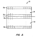
- a CRT screen 26 is shown.
- Data stored in video memories are often organized for convenient display on a CRT screen.
- a row of memory may, e.g., consist of 16-bit information designed to display a specific group of pixels on the CRT screen.
- the CRT screen 26 is defined as having a top half 28 and a bottom half 30.
- Data from even numbered arrays is displayed in the top half 28 of the CRT 26, while data from the odd numbered arrays (e.g., ARRAY1, ARRAY3, etc.) is displayed in the bottom half 30 of the CRT 26.
- the memory device 10 is addressed for the display of any information in the top half of the screen 28, one of the even numbered arrays will be addressed. None of the odd numbered arrays will be addressed for that request.
- This permits the word lines WL for adjacently numbered arrays (e.g., ARRAY0 and ARRAY1) to share bootstrap circuits 16, as ARRAY0 will not be selected at the same time as ARRAY1 and vice versa. The result is a savings in valuable die space.
- ARRAY0 data from the first row (WL00) of ARRAY0 is designated to be output on a first row 28a of the top half 28 of the CRT 26 and that data from the first row (WL10) of ARRAY1 is designated to be output on row 30a of the CRT screen 26.
- ARRAY0 is accessed, and the row decode circuitry 18a asserts word line WL00.
- Word line WL00 is boosted by bootstrap circuit 16a.
- bootstrap circuit 16a is also shared by word line WL10, there is no chance that both word lines will be asserted at the same time, as the data from the two word lines is designated to be display on different portions of the CRT screen 26.
- the remainder of the CRT screen 26 and the memory arrays 14 may be segmented in a similar manner.
- the present invention may be embodied in other specific forms without departing from the characteristics thereof.
- array arrangements including matrices of arrays
- Other numbering schemes of arrays may also be used, so long as at least two arrays share bootstrap circuits. Further savings in area may be realized by sharing bootstrap circuits from, e.g., three arrays.
Landscapes
- Engineering & Computer Science (AREA)
- Microelectronics & Electronic Packaging (AREA)
- Computer Hardware Design (AREA)
- Dram (AREA)
- Control Of Indicators Other Than Cathode Ray Tubes (AREA)
- Static Random-Access Memory (AREA)
Description
- The present invention relates to semiconductor memories. More particularly, the present invention relates to word line bootstrap circuits used in semiconductor memories.
- Random access semiconductor memories are an important and integral part of todays electronic systems. These memories are commonly arranged in a number of arrays, each array addressable by row and column decode circuitry. Row decoders select word lines while column decoders select bit lines. Existing random access semiconductor memory designs require that a booststrap circuit be coupled to each and every word line of each array of the memory device. These bootstrap circuits are designed to boost a selected word line from, e.g., Vss to 1.5*Vcc. Those skilled in the art will recognize that a number of bootstrap circuits exist which may be used for this purpose. All, however, require the use of a capacitive circuit to store charge for the boost. That is, for every single word line in a memory array, a single capacitive bootstrap circuit is required.
- The areal size of the bootstrap circuit, related to the capacitance needed, depends upon the number of bit and
bit lines driven by a given word line. For example, in an array having 512 bit lines and 512bit lines, a bootstrap circuit should be able to store sufficient charge to drive the 1024 total bit lines and the word line to, e.g., 1.5*Vcc. A capacitive bootstrap circuit of this size, coupled to every word line in a memory can consume an economically significant amount of die area. - Considering that a typical array may include 256 to 512 word lines and that memories commonly are designed with a number of arrays (e.g., 16), the number of bootstrap circuits needed can be quite large. It is desireable to reduce the number of bootstrap circuits used in a memory design to free valuable die area.
- One use for random access memories is to store video data. Video memory devices, such as video random access memories (RAMs) or frame buffer memories, have become an important and integral part of many computer systems. These devices often include a RAM portion to store data representing pixel data to be displayed on a display device. Thus, the RAM portion of the device is generally formed to have a bit width compatible with the display of a certain amount of pixel data. For example, many memory devices use a number of 256 bit wide memory arrays. 256 bits can, e.g., be used to represent 32 pixels having 8 bits of data, or can represent 16 pixels formed from 16 bits of data. This pixel data may be displayed on a cathode ray tube (CRT) screen or otherwise manipulated. Many of these video memories, however, are expensive to manufacture as they occupy a relatively large amount of die area. It is desireable to conserve the die area occupied by these video memories.
- The invention is defined in the
claims 1, 6 and 7. - The present invention offers a memory device which occupies a smaller area than previous devices.
- A memory device according to the invention includes at least first and second memory arrays each having a number of word lines. Each of the word lines are coupled to a shared word line bootstrap circuit so that every word line from the first array shares a bootstrap circuit with a word line from the second array.
- Devices according to the invention may be implemented in memories having a number of arrays. Every pair of arrays uses common or shared bootstrap circuits, thereby reducing the number of capacitive bootstrap circuits by 1/2, resulting in a relatively substantial savings in die area.
- In one embodiment, bootstrap circuits are shared in a video memory device which has a number of arrays. One group of arrays is designated to store video information for, e.g., a top portion of a display screen, while a second group of arrays is designated to store video information for, e.g., a bottom portion of the display screen. Arrays from the first group share bootstrap circuits with arrays from the second group. The result is a video memory implemented with a relatively substantial savings in die area.
- For a fuller understanding of the nature and advantages of the invention, reference should be made to the ensuing description taken in conjunction with the accompanying drawings.
- Fig. 1 is a block diagram depicting a generalized memory system using shared bootstrap circuits according to the present invention; and
- Fig. 2 illustrates a display screen divided into portions for use with the memory system of Fig. 1.
-
- Features of the present invention will be discussed by first referring to Fig. 1 where a simplified portion of a typical memory device 10 is shown. The memory device 10 includes a number of memory arrays 14 addressed by row decode 18 and column decode 22 circuitry. The portion of memory device 10 shown may be implemented in any of a number of random access memory (RAM) architectures known to those skilled in the art. Preferably, memory device 10 is implemented in a video RAM or in a frame buffer memory adapted to store pixel information for processing or for display on a CRT screen.
- The memory device 10 includes a number of arrays 14 (labelled ARRAY0-ARRAYN) having memory cells arranged in rows and columns. A number of configurations and arrangements of these arrays are known in the art, therefore a detailed description will not be given, instead, a simple column of arrays is shown for discussion. A row address signal is applied to a selected array 14 via a row address decoder 18. The row address decoder 18 selects a specific word line WL of a selected array. When a word line is selected, a bootstrap circuit 16 coupled to the word line boosts the word line from Vss to, e.g., 1.5*Vcc. This voltage boost operates pass transistors along the selected word line, allowing charge stored in each memory cell to be passed to the bit and
bit lines. Each bit andbit line combination is sensed by sense amplifier circuitry 12 to generate output signals amplified by read/write circuitry 20. The data may then be passed, e.g., to a CRT for display via global address anddata lines 24. In the configuration depicted, the arrays are positioned so that neighboring arrays share sense amplifiers. This configuration is commonly known in the art and a detailed description will not be given. Further, those skilled in the art, upon reading this disclosure, will recognize that features of the present invention may be implemented in arrays which do not share sense amplifiers. - According to the invention, the bootstrap circuits 16 used are coupled to two separate word lines WL. That is, each bootstrap circuit 16 is shared by two memory arrays. For example, memory arrays ARRAY0 and ARRAY1 may share bootstrap circuits 16. Each word line of ARRAY0 shares a bootstrap circuit 16 with a corresponding word line in ARRAY1. For example, word line WL00 of ARRAY0 shares a bootstrap circuit 16a with word line WL10 of ARRAY1, while word line WLON shares a
bootstrap circuit 16b with word line WL1N. This reduces the number of capacitive bootstrap circuits by approximately 1/2 over previous designs, thereby freeing valuable die space. - In one embodiment, the memory arrays 14 are numbered such that every even numbered array (e.g., ARRAY0, ARRAY2, ARRAY4, etc.) shares bootstrap circuits with an odd numbered array (e.g., ARRAY1, ARRAY3, etc.), although any array numbering scheme may be used so long as arrays which share bootstrap circuits are not selected simultaneously.
- One approach to ensuring that adjacent arrays are not simultaneously selected will now be described by referring to Fig. 2, where a
CRT screen 26 is shown. Data stored in video memories are often organized for convenient display on a CRT screen. A row of memory may, e.g., consist of 16-bit information designed to display a specific group of pixels on the CRT screen. In one embodiment of the present invention, theCRT screen 26 is defined as having atop half 28 and abottom half 30. Data from even numbered arrays (e.g., ARRAY0, ARRAY2, ARRAY4, etc.) is displayed in thetop half 28 of theCRT 26, while data from the odd numbered arrays (e.g., ARRAY1, ARRAY3, etc.) is displayed in thebottom half 30 of theCRT 26. If the memory device 10 is addressed for the display of any information in the top half of thescreen 28, one of the even numbered arrays will be addressed. None of the odd numbered arrays will be addressed for that request. This permits the word lines WL for adjacently numbered arrays (e.g., ARRAY0 and ARRAY1) to share bootstrap circuits 16, as ARRAY0 will not be selected at the same time as ARRAY1 and vice versa. The result is a savings in valuable die space. - As an example, assume that data from the first row (WL00) of ARRAY0 is designated to be output on a first row 28a of the
top half 28 of theCRT 26 and that data from the first row (WL10) of ARRAY1 is designated to be output on row 30a of theCRT screen 26. When row 28a of theCRT 26 is to be refreshed, ARRAY0 is accessed, and therow decode circuitry 18a asserts word line WL00. Word line WL00 is boosted by bootstrap circuit 16a. Although bootstrap circuit 16a is also shared by word line WL10, there is no chance that both word lines will be asserted at the same time, as the data from the two word lines is designated to be display on different portions of theCRT screen 26. The remainder of theCRT screen 26 and the memory arrays 14 may be segmented in a similar manner. - As will now be appreciated by those familiar with the art, the present invention may be embodied in other specific forms without departing from the characteristics thereof. For example, although a simple columnar arrangement of arrays is shown herein, other array arrangements (including matrices of arrays) may also be used so long as bootstrap circuits are shared between arrays. Other numbering schemes of arrays may also be used, so long as at least two arrays share bootstrap circuits. Further savings in area may be realized by sharing bootstrap circuits from, e.g., three arrays. While the shared bootstrap arrangement has been described for use in video memories, those skilled in the art will now recognize that the shared bootstrap arrangement of the present invention may be implemented in other memories as well so long as some provision is made to prevent word lines which share bootstrap circuits from being accessed at the same time. Further, while adjacent arrays are shown as sharing bootstrap circuits, arrays which are not physically or even logically adjacent may also share bootstrap circuits.
- Accordingly, the disclosure of the invention is intended to be illustrative, but not limiting, of the scope of the invention which is set forth in the following claims.
Claims (7)
- A memory device, comprising:at least a first and a second memory array (14), each having a plurality of word lines (WL); anda plurality of word line bootstrap circuits (16), each of said word line bootstrap circuits (16) coupled to a word line (WL) from said frist memory array (14) and to a word line (WL) from said second memory array (14).
- The memory device of claim 1, further comprising:at least a third and a fourth memory array (14), each having a plurality of word lines (WL);a second plurality of word line bootstrap circuits (16), each of said second plurality of word line bootstrap circuits (16) coupled to a word line (WL) from said third memory array (14) and a word line from said fourth memory array (14).
- The memory device of claim 2, wherein data stored in said first and third arrays (14) is stored for display on a first portion of a video display screen (26).
- The memory device of claim 3, wherein data stored in said second and fourth arrays (14) is stored for display on a second portion of a video display screen (26).
- The memory device of claim 3, wherein said first portion of video display screen is the top half (28) of said screen (26).
- A video memory device, comprising:a plurality of memory arrays (14), each of said memory arrays (14) identifiable by a sequentially numbered address, and each having a number of word lines (WL); anda plurality of bootstrap circuits (16), each of said bootstrap circuits (16) coupled to a word line (WL) from both an odd numbered one and an even numbered one of said memory arrays (14).
- A method of displaying video information stored in a video memory (10) having a plurality of memory arrays (14) each having a number of word lines (WL), the method comprising the steps of :addressing said video memory (10) by addressing a first word line (WL) in a first memory array (14a);boosting, using a first bootstrap circuit (16a, 16b), a voltage level of said first wordline of said first array;outputting, from said first memory array (14a), first video information stored in memory cells along said first word line (WL);displaying said first video information on a first portion (28) of a video screen (26);addressing said video memory (10) by addressing a second word line (WL) in a second memory array (14b);boosting, using said first bootstrap circuit (16a, 16b), a voltage level of said second word line of said second memory array (14b);outputting, from said second memory array (14b), second video information stored in memory cells along said second word line (WL); anddisplaying said second video information on a second portion (30) of said video screen (26).
Applications Claiming Priority (2)
| Application Number | Priority Date | Filing Date | Title |
|---|---|---|---|
| US08/656,165 US5793383A (en) | 1996-05-31 | 1996-05-31 | Shared bootstrap circuit |
| US656165 | 1996-05-31 |
Publications (3)
| Publication Number | Publication Date |
|---|---|
| EP0810608A2 EP0810608A2 (en) | 1997-12-03 |
| EP0810608A3 EP0810608A3 (en) | 1999-07-14 |
| EP0810608B1 true EP0810608B1 (en) | 2002-07-31 |
Family
ID=24631922
Family Applications (1)
| Application Number | Title | Priority Date | Filing Date |
|---|---|---|---|
| EP97108266A Expired - Lifetime EP0810608B1 (en) | 1996-05-31 | 1997-05-22 | Shared bootstrap circuit |
Country Status (7)
| Country | Link |
|---|---|
| US (1) | US5793383A (en) |
| EP (1) | EP0810608B1 (en) |
| JP (1) | JPH1055671A (en) |
| KR (1) | KR970076852A (en) |
| CN (1) | CN1117377C (en) |
| DE (1) | DE69714350T2 (en) |
| TW (1) | TW357347B (en) |
Families Citing this family (2)
| Publication number | Priority date | Publication date | Assignee | Title |
|---|---|---|---|---|
| US6947100B1 (en) * | 1996-08-09 | 2005-09-20 | Robert J. Proebsting | High speed video frame buffer |
| US11024393B1 (en) | 2020-01-09 | 2021-06-01 | Sandisk Technologies Llc | Read operation for non-volatile memory with compensation for adjacent wordline |
Family Cites Families (13)
| Publication number | Priority date | Publication date | Assignee | Title |
|---|---|---|---|---|
| US4503522A (en) * | 1981-03-17 | 1985-03-05 | Hitachi, Ltd. | Dynamic type semiconductor monolithic memory |
| US4570239A (en) * | 1983-01-24 | 1986-02-11 | Motorola, Inc. | Series read-only-memory having capacitive bootstrap precharging circuitry |
| JP2547615B2 (en) * | 1988-06-16 | 1996-10-23 | 三菱電機株式会社 | Read-only semiconductor memory device and semiconductor memory device |
| KR920010344B1 (en) * | 1989-12-29 | 1992-11-27 | 삼성전자주식회사 | Memory array composition method |
| US5285407A (en) * | 1991-12-31 | 1994-02-08 | Texas Instruments Incorporated | Memory circuit for spatial light modulator |
| US5276650A (en) * | 1992-07-29 | 1994-01-04 | Intel Corporation | Memory array size reduction |
| JP2833359B2 (en) * | 1992-07-29 | 1998-12-09 | 日本電気株式会社 | DRAM circuit |
| US5265050A (en) * | 1992-08-18 | 1993-11-23 | Micron Technology, Inc. | Integrated circuit memory with isolation of column line portions through P-sense amplification period |
| JPH06139776A (en) * | 1992-10-23 | 1994-05-20 | Fujitsu Ltd | Semiconductor storage device |
| JP3068352B2 (en) * | 1992-12-01 | 2000-07-24 | 日本電気株式会社 | Semiconductor memory |
| US5327026A (en) * | 1993-02-17 | 1994-07-05 | United Memories, Inc. | Self-timed bootstrap decoder |
| JP2725570B2 (en) * | 1993-11-02 | 1998-03-11 | 日本電気株式会社 | Semiconductor memory device |
| JP3080829B2 (en) * | 1994-02-17 | 2000-08-28 | 株式会社東芝 | Multi-bank synchronous memory system with cascaded memory cell structure |
-
1996
- 1996-05-31 US US08/656,165 patent/US5793383A/en not_active Expired - Lifetime
-
1997
- 1997-04-17 TW TW086105125A patent/TW357347B/en not_active IP Right Cessation
- 1997-05-22 DE DE69714350T patent/DE69714350T2/en not_active Expired - Lifetime
- 1997-05-22 EP EP97108266A patent/EP0810608B1/en not_active Expired - Lifetime
- 1997-05-23 KR KR1019970020263A patent/KR970076852A/en not_active Application Discontinuation
- 1997-05-29 CN CN97112164A patent/CN1117377C/en not_active Expired - Fee Related
- 1997-06-02 JP JP9143750A patent/JPH1055671A/en active Pending
Also Published As
| Publication number | Publication date |
|---|---|
| CN1175773A (en) | 1998-03-11 |
| JPH1055671A (en) | 1998-02-24 |
| KR970076852A (en) | 1997-12-12 |
| DE69714350D1 (en) | 2002-09-05 |
| DE69714350T2 (en) | 2003-02-13 |
| EP0810608A3 (en) | 1999-07-14 |
| US5793383A (en) | 1998-08-11 |
| TW357347B (en) | 1999-05-01 |
| CN1117377C (en) | 2003-08-06 |
| EP0810608A2 (en) | 1997-12-03 |
Similar Documents
| Publication | Publication Date | Title |
|---|---|---|
| EP0803124B1 (en) | A dual bank memory and systems using the same | |
| EP0781443B1 (en) | Memory device and data processing system with such a memory device | |
| US4677592A (en) | Dynamic RAM | |
| US7609573B2 (en) | Embedded memory databus architecture | |
| JP3048498B2 (en) | Semiconductor storage device | |
| US5812483A (en) | Integrated circuit memory devices including split word lines and predecoders and related methods | |
| US4896294A (en) | Semiconductor memory device with row and column word lines and row and column bit lines | |
| US6314048B1 (en) | Semiconductor memory device for fast access | |
| US5978302A (en) | Multi-bank architecture for a wide I/O DRAM | |
| US5586080A (en) | Local word line phase driver | |
| US5383160A (en) | Dynamic random access memory | |
| EP0810608B1 (en) | Shared bootstrap circuit | |
| US6563749B2 (en) | Dynamic memory circuit including spare cells | |
| US6031783A (en) | High speed video frame buffer | |
| US5740116A (en) | Current limiting during block writes of memory circuits | |
| US6493284B2 (en) | Semiconductor memory device having hierarchical wordline structure | |
| US6028811A (en) | Architecture for high bandwidth wide I/O memory devices | |
| US6970389B2 (en) | Integrated memory | |
| US6947100B1 (en) | High speed video frame buffer | |
| US6327169B1 (en) | Multiple bit line memory architecture | |
| JPH08221975A (en) | Semiconductor memory circuit | |
| US6026044A (en) | High speed video frame buffer | |
| KR100217281B1 (en) | Pdp-tv using sdram interface equipment | |
| JPH0554644A (en) | Semiconductor memory | |
| JP2001093281A (en) | Semiconductor memory |
Legal Events
| Date | Code | Title | Description |
|---|---|---|---|
| PUAI | Public reference made under article 153(3) epc to a published international application that has entered the european phase |
Free format text: ORIGINAL CODE: 0009012 |
|
| AK | Designated contracting states |
Kind code of ref document: A2 Designated state(s): DE GB NL |
|
| PUAL | Search report despatched |
Free format text: ORIGINAL CODE: 0009013 |
|
| AK | Designated contracting states |
Kind code of ref document: A3 Designated state(s): DE GB NL |
|
| 17P | Request for examination filed |
Effective date: 19991230 |
|
| GRAG | Despatch of communication of intention to grant |
Free format text: ORIGINAL CODE: EPIDOS AGRA |
|
| 17Q | First examination report despatched |
Effective date: 20010719 |
|
| GRAG | Despatch of communication of intention to grant |
Free format text: ORIGINAL CODE: EPIDOS AGRA |
|
| GRAH | Despatch of communication of intention to grant a patent |
Free format text: ORIGINAL CODE: EPIDOS IGRA |
|
| GRAH | Despatch of communication of intention to grant a patent |
Free format text: ORIGINAL CODE: EPIDOS IGRA |
|
| GRAA | (expected) grant |
Free format text: ORIGINAL CODE: 0009210 |
|
| AK | Designated contracting states |
Kind code of ref document: B1 Designated state(s): DE GB NL |
|
| REG | Reference to a national code |
Ref country code: GB Ref legal event code: FG4D |
|
| REF | Corresponds to: |
Ref document number: 69714350 Country of ref document: DE Date of ref document: 20020905 |
|
| PLBE | No opposition filed within time limit |
Free format text: ORIGINAL CODE: 0009261 |
|
| STAA | Information on the status of an ep patent application or granted ep patent |
Free format text: STATUS: NO OPPOSITION FILED WITHIN TIME LIMIT |
|
| 26N | No opposition filed |
Effective date: 20030506 |
|
| PGFP | Annual fee paid to national office [announced via postgrant information from national office to epo] |
Ref country code: NL Payment date: 20080515 Year of fee payment: 12 |
|
| NLV4 | Nl: lapsed or anulled due to non-payment of the annual fee |
Effective date: 20091201 |
|
| PG25 | Lapsed in a contracting state [announced via postgrant information from national office to epo] |
Ref country code: NL Free format text: LAPSE BECAUSE OF NON-PAYMENT OF DUE FEES Effective date: 20091201 |
|
| REG | Reference to a national code |
Ref country code: GB Ref legal event code: 732E Free format text: REGISTERED BETWEEN 20101111 AND 20101117 |
|
| REG | Reference to a national code |
Ref country code: GB Ref legal event code: 732E Free format text: REGISTERED BETWEEN 20110303 AND 20110309 |
|
| REG | Reference to a national code |
Ref country code: DE Ref legal event code: R081 Ref document number: 69714350 Country of ref document: DE Owner name: INTELLECTUAL VENTURES ILLC ( N. D. GES. D. STA, US Free format text: FORMER OWNER: PRFA TECHNOLOGY FUND, LLC., WILMINGTON, DEL., US Effective date: 20110228 Ref country code: DE Ref legal event code: R081 Ref document number: 69714350 Country of ref document: DE Owner name: INTELLECTUAL VENTURES ILLC ( N. D. GES. D. STA, US Free format text: FORMER OWNER: PRFA TECHNOLOGY FUND, LLC., WILMINGTON, US Effective date: 20110228 |
|
| PGFP | Annual fee paid to national office [announced via postgrant information from national office to epo] |
Ref country code: DE Payment date: 20110531 Year of fee payment: 15 |
|
| PGFP | Annual fee paid to national office [announced via postgrant information from national office to epo] |
Ref country code: GB Payment date: 20120426 Year of fee payment: 16 |
|
| REG | Reference to a national code |
Ref country code: DE Ref legal event code: R119 Ref document number: 69714350 Country of ref document: DE Effective date: 20121201 |
|
| PG25 | Lapsed in a contracting state [announced via postgrant information from national office to epo] |
Ref country code: DE Free format text: LAPSE BECAUSE OF NON-PAYMENT OF DUE FEES Effective date: 20121201 |
|
| GBPC | Gb: european patent ceased through non-payment of renewal fee |
Effective date: 20130522 |
|
| PG25 | Lapsed in a contracting state [announced via postgrant information from national office to epo] |
Ref country code: GB Free format text: LAPSE BECAUSE OF NON-PAYMENT OF DUE FEES Effective date: 20130522 |