EP0809885B1 - Circuit configuration for feeding a pulse output stage - Google Patents
Circuit configuration for feeding a pulse output stage Download PDFInfo
- Publication number
- EP0809885B1 EP0809885B1 EP96941057A EP96941057A EP0809885B1 EP 0809885 B1 EP0809885 B1 EP 0809885B1 EP 96941057 A EP96941057 A EP 96941057A EP 96941057 A EP96941057 A EP 96941057A EP 0809885 B1 EP0809885 B1 EP 0809885B1
- Authority
- EP
- European Patent Office
- Prior art keywords
- capacitor
- output stage
- pulse
- switching means
- circuit configuration
- Prior art date
- Legal status (The legal status is an assumption and is not a legal conclusion. Google has not performed a legal analysis and makes no representation as to the accuracy of the status listed.)
- Expired - Lifetime
Links
- 239000003990 capacitor Substances 0.000 claims abstract description 55
- 230000000295 complement effect Effects 0.000 description 3
- 238000010586 diagram Methods 0.000 description 3
- 238000004804 winding Methods 0.000 description 3
- 230000001965 increasing effect Effects 0.000 description 2
- 239000000463 material Substances 0.000 description 2
- 230000001681 protective effect Effects 0.000 description 2
- 230000001360 synchronised effect Effects 0.000 description 2
- 230000001960 triggered effect Effects 0.000 description 2
- 240000000731 Fagus sylvatica Species 0.000 description 1
- 235000010099 Fagus sylvatica Nutrition 0.000 description 1
- 230000000903 blocking effect Effects 0.000 description 1
- 230000006866 deterioration Effects 0.000 description 1
- 230000005611 electricity Effects 0.000 description 1
- 238000004146 energy storage Methods 0.000 description 1
- 238000005516 engineering process Methods 0.000 description 1
- 230000005284 excitation Effects 0.000 description 1
- 230000002349 favourable effect Effects 0.000 description 1
- 230000005669 field effect Effects 0.000 description 1
- 230000001939 inductive effect Effects 0.000 description 1
- 230000010363 phase shift Effects 0.000 description 1
- 239000002574 poison Substances 0.000 description 1
- 231100000614 poison Toxicity 0.000 description 1
- 238000004513 sizing Methods 0.000 description 1
- 230000009466 transformation Effects 0.000 description 1
Images


Classifications
-
- H—ELECTRICITY
- H03—ELECTRONIC CIRCUITRY
- H03K—PULSE TECHNIQUE
- H03K3/00—Circuits for generating electric pulses; Monostable, bistable or multistable circuits
- H03K3/02—Generators characterised by the type of circuit or by the means used for producing pulses
- H03K3/53—Generators characterised by the type of circuit or by the means used for producing pulses by the use of an energy-accumulating element discharged through the load by a switching device controlled by an external signal and not incorporating positive feedback
- H03K3/57—Generators characterised by the type of circuit or by the means used for producing pulses by the use of an energy-accumulating element discharged through the load by a switching device controlled by an external signal and not incorporating positive feedback the switching device being a semiconductor device
-
- H—ELECTRICITY
- H01—ELECTRIC ELEMENTS
- H01S—DEVICES USING THE PROCESS OF LIGHT AMPLIFICATION BY STIMULATED EMISSION OF RADIATION [LASER] TO AMPLIFY OR GENERATE LIGHT; DEVICES USING STIMULATED EMISSION OF ELECTROMAGNETIC RADIATION IN WAVE RANGES OTHER THAN OPTICAL
- H01S5/00—Semiconductor lasers
- H01S5/04—Processes or apparatus for excitation, e.g. pumping, e.g. by electron beams
- H01S5/042—Electrical excitation ; Circuits therefor
-
- H—ELECTRICITY
- H02—GENERATION; CONVERSION OR DISTRIBUTION OF ELECTRIC POWER
- H02M—APPARATUS FOR CONVERSION BETWEEN AC AND AC, BETWEEN AC AND DC, OR BETWEEN DC AND DC, AND FOR USE WITH MAINS OR SIMILAR POWER SUPPLY SYSTEMS; CONVERSION OF DC OR AC INPUT POWER INTO SURGE OUTPUT POWER; CONTROL OR REGULATION THEREOF
- H02M3/00—Conversion of dc power input into dc power output
- H02M3/02—Conversion of dc power input into dc power output without intermediate conversion into ac
- H02M3/04—Conversion of dc power input into dc power output without intermediate conversion into ac by static converters
- H02M3/10—Conversion of dc power input into dc power output without intermediate conversion into ac by static converters using discharge tubes with control electrode or semiconductor devices with control electrode
-
- H—ELECTRICITY
- H01—ELECTRIC ELEMENTS
- H01S—DEVICES USING THE PROCESS OF LIGHT AMPLIFICATION BY STIMULATED EMISSION OF RADIATION [LASER] TO AMPLIFY OR GENERATE LIGHT; DEVICES USING STIMULATED EMISSION OF ELECTROMAGNETIC RADIATION IN WAVE RANGES OTHER THAN OPTICAL
- H01S5/00—Semiconductor lasers
- H01S5/04—Processes or apparatus for excitation, e.g. pumping, e.g. by electron beams
- H01S5/042—Electrical excitation ; Circuits therefor
- H01S5/0428—Electrical excitation ; Circuits therefor for applying pulses to the laser
Definitions
- the invention relates to a circuit arrangement for feeding a Pulse output stage with the features of the preamble of claims 1 to 3.
- a circuit arrangement of this type is known from DE 23 31 084 C2.
- the Inductance is designed as a flyback transformer, in which the Primary winding of a transformer with a low voltage source over a pulse-controlled transistor switching device is connected.
- the Secondary winding is with the capacitor through a rectifier arrangement connected.
- the pulse control device consists of an arrangement for specifying the Transistor base voltage and a feedback circuit from the transformer to Base of the transistor. These form a self-oscillating circle in which the transistor periodically from control pulses during a specific Time interval is controlled.
- the duration of the time interval can be determined by Variation of the gear ratio for the base voltage of the Transistor or variation of the source voltage can be set. she determines the amount of energy stored in the transformer Capacitor can be transferred.
- the current tax times of the Transistors for the conductive and blocking state are exclusive through the primary-side oscillator components and the resonant circuit in the Secondary circuit determined.
- the control pulse train of the transistor is also used for generation of synchronous control pulses in the discharge path of the capacitor used.
- the triggering of the useful pulses therefore also depends on the primary-side oscillator components.
- a voltage source that is high Provides voltage directly charges a capacitor via an inductor the voltage of the voltage source. By closing a switch the capacitor is discharged in the form of a useful pulse which leads to pulsed excitation of a gas laser is used. The switch opens then depending on the discharge status of the capacitor. The amplitude of the discharge pulse cannot be adjusted. The charging cycle hangs depending on the operating conditions.
- Power amplifiers of the type mentioned at the beginning of low voltage pulses with low Internal resistance enable, for example, the energy supply by consumers who are to be operated in pulsed fashion.
- consumers are pulse diode lasers.
- pulse voltages up to 100 volts. With larger pulse powers much higher voltages are necessary.
- Pulse repetition frequencies of several 10 kHz are common here.
- an amplitude setting is made by changing the Impulse voltage required.
- Thyristors are often used for such output stages (cf. UNITRODE Inc., Designnote 15) or MOS power transistors, such as. B. MOS field effect transistors (MOS-FET) used (cf. SILICONIX Inc., Application note '6.13.10 Laser Diode Pulsers').
- MOS-FET MOS field effect transistors
- SILICONIX Inc. Application note '6.13.10 Laser Diode Pulsers'.
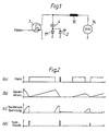
- Such usually Circuit arrangement used is in Fig. 7 and 8 using the example of a Control for a diode laser shown for explanation.
- a capacitor 4 and a switching device in the form of a MOS-FET 1 (Fig. 7) or thyristor 6 (Fig. 8) are in series connected.
- the capacitor 4 is connected by a charging circuit 3 (FIG. 7) or 5 (Fig.
- the charging voltage is provided by a voltage source 7 by a transistor (Fig. 7) or MOS-FET (Fig. 8) as a switching element 8 via a resistor 9, which here should include all lead impedances and internal resistances, is connected to the capacitor 4, as shown in FIGS. 7 and 8.
- a protective diode 11 with opposite poles parallel to the diode laser 2 connected.
- the MOS-FET 1 or the thyristor 6 When the MOS-FET 1 or the thyristor 6 is activated, it switches the diode laser 2 to the charged capacitor 4. This is by one by the diode laser 2 and the MOS-FET 1 or thyristor 6 flowing current pulse almost completely discharged. The recharge of the Capacitor 4 can be made in the pulse pauses of the control pulses become.
- An amplitude setting can also be used at high pulse repetition frequencies be carried out by the switching element 8 is controlled by a pulse width modulated signal, so that by the different charging time of the capacitor 4 to the corresponding Final voltage is loaded.
- This final tension is not linear from the Charging time depends, but follows an exponential function. Remedy would an additional increase in high voltage or / and a Bring constant current source circuit. However, the increased bring Circuit effort and the further deterioration of the electrical Efficiency combined with additional costs, others Disadvantages with it.
- Another disadvantage is the realization of the fast electronic Switch for the high voltage, which also energy loss and costs.
- the invention was based, the charge voltage of the task Capacitor for each useful pulse regardless of the To be able to set pulse repetition frequency.
- the inventive Circuit arrangement for supplying a pulse output stage Energy supply to an output stage in the high-pause Efficiency, especially at low supply voltages There is no additional DC voltage source for the high voltage required.
- the circuit arrangement according to the invention offers a easy way to be able to adjust the amplitude linearly, whereby a quick setting from pulse to pulse can also be made can. Overall, there is a reduction in material and costs as well an increase in electrical efficiency.
- the voltage supply is fundamentally different consists of a low voltage source 14, an inductance via having coil 10 a low voltage from the low voltage source 14 (e.g. 5 volts of a battery) directly to the pulse output stage, that is without significant losses.
- the switching device 1 The MOS-FET used can be controlled via pulse width modulated PWM pulses become. The MOS-FET is switched through in the pulse pauses, see above that a linearly increasing current flow can build up in the coil 10.
- the capacitor 4 which in a previous cycle has already been loaded, in the form of the useful pulse via the as an output stage Discharge 2 used diode lasers in pulses.
- the capacitor 4 forms with the coil 10 a resonant circuit with the period T.
- FIG. 2 To complement FIG. 1, some signal profiles are shown in FIG. 2, with (a) different pulse width modulated pulses, with (b) the current flowing through the coil 10, at (c) the corresponding current Capacitor voltage and at (d) the useful pulse is shown.
- the circuit arrangement 1 is characterized by its simplicity. Because in practice the Components are not ideal, losses occur, which are mainly due to the Charging branch 11 arranged rectifying or protective diode, as well as on the Starting resistance of the MOS-FET and the quality of the resonant circuit are due. Efficiencies of over 80%, with more reasonable ones Sizing can be achieved without difficulty. Modern components very good quality, such as using fast low power MOS FET ON resistances of less than 0.1 ohms are now becoming very inexpensive offered on the market. Corresponding poison for the others Components.
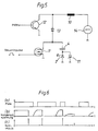
- the output stage 2 comprises one Series connection from a thyristor used as a triggerable switch 6 and a diode laser as a consumer.
- the free connection of the diode laser is connected to a capacitor 4.
- the connection point of diode laser and capacitor 4 is on the one hand with an inductance having coil 10 and on the other hand with a switching device 12 used transistor connected so that this parallel to the Series connection of thyristor and diode laser is connected.
- the coil 10 is with its free connection to a voltage source 14 for a supply voltage connected.
- the pulse width modulated signal PWM is on here laid the base of the transistor to the when the transistor is turned on Coil 10 connect the supply voltage of the voltage source 14.
- the further trigger signal is applied to the thyristor as a trigger signal and only used for pulse triggering.
- circuit arrangement described above can be used with all output stages can be used in which the combined function as shown in Fig. 1 is not suitable. In the case of the output stage with thyristor, this takes over additional transistor now clearing the thyristor. The additional costs are negligible since this transistor is usually can be a cheap type.
- FIG. 4 To complement FIG. 3, some signal curves are shown in FIG. 4, where (a) pulse width modulated pulses PWM, (b) the voltage at Capacitor 4 and at (c) the trigger pulse is shown. You can see that when the transistor is turned on, the voltage on the capacitor 4 on the Is reference potential. i.e. here on earth.
- the first embodiment according to FIG. 1 can do so be modified outside of the time during which the energy is off the coil 10 is supplied to the capacitor 4 at any time a pulse generation can be triggered.
- connection point of capacitor 4 and a switch device 1 ' which can be controlled as a second provided MOS-FET not directly, but via a diode 13 with the Coil 10 connected.
- Parallel to the pulse output stage is an as Switching device 12 provided transistor switched with pulse width modulated pulses (PWM) can be controlled. If the Transistor is turned on, the coil 10 is the supply voltage the voltage source 14 connected.
- PWM pulse width modulated pulses
- FIG. 6 To complement FIG. 5, some signal curves are shown in FIG. 6, which demonstrate the great flexibility that is now available should.
- PWM pulse width modulated pulses
- FIG. 6 To complement FIG. 5, some signal curves are shown in FIG. 6, which demonstrate the great flexibility that is now available should.
- PWM pulse width modulated pulses
Landscapes
- Physics & Mathematics (AREA)
- Engineering & Computer Science (AREA)
- Power Engineering (AREA)
- Condensed Matter Physics & Semiconductors (AREA)
- General Physics & Mathematics (AREA)
- Electromagnetism (AREA)
- Optics & Photonics (AREA)
- Lasers (AREA)
- Generation Of Surge Voltage And Current (AREA)
- Dc-Dc Converters (AREA)
- Semiconductor Lasers (AREA)
Abstract
Description
Die Erfindung betrifft eine Schaltungsanordnung zur Speisung einer
Impulsendstufe mit den Merkmalen des Oberbegriffs der Ansprüche 1 bis 3.The invention relates to a circuit arrangement for feeding a
Pulse output stage with the features of the preamble of
Eine Schaltungsanordnung dieser Art ist aus DE 23 31 084 C2 bekannt. Die Induktivität ist als Sperrwandlerüberträger ausgebildet, bei dem die Primärwicklung eines Transformators mit einer Niederspannungsquelle über eine impulsgesteuerte Transistorschalteinrichtung verbunden ist. Die Sekundärwicklung ist mit dem Kondensator über eine Gleichrichteranordnung verbunden.A circuit arrangement of this type is known from DE 23 31 084 C2. The Inductance is designed as a flyback transformer, in which the Primary winding of a transformer with a low voltage source over a pulse-controlled transistor switching device is connected. The Secondary winding is with the capacitor through a rectifier arrangement connected.
Die Impulssteuereinrichtung besteht aus einer Anordnung zur Vorgabe der Transistorbasisspannung und einem Rückführkreis vom Transformator zur Basis des Transistors. Diese bilden einen selbstschwingenden Kreis, in dem der Transistor periodisch von Steuerimpulsen während eines spezifischen Zeitintervalls leitend gesteuert wird. Die Dauer des Zeitintervalls kann durch Variation des Übersetzungsverhältnisses für die Basisspannung des Transistors oder Variation der Quettenspannung eingestellt werden. Sie bestimmt den im Transformator gespeicherten Energiebetrag, der in den Kondensator übertragen werden kann. Die aktuellen Steuerzeitpunkte des Transistors für den leitenden und sperrenden Zustand werden ausschließlich durch die primärseitigen Oszillatorbauteile und das Schwingkreisvefiatten im Sekundärkreis bestimmt.The pulse control device consists of an arrangement for specifying the Transistor base voltage and a feedback circuit from the transformer to Base of the transistor. These form a self-oscillating circle in which the transistor periodically from control pulses during a specific Time interval is controlled. The duration of the time interval can be determined by Variation of the gear ratio for the base voltage of the Transistor or variation of the source voltage can be set. she determines the amount of energy stored in the transformer Capacitor can be transferred. The current tax times of the Transistors for the conductive and blocking state are exclusive through the primary-side oscillator components and the resonant circuit in the Secondary circuit determined.
Im gesperrten Zustand des Transistors wird die im Transformator gespeicherte Energie über die Sekundärwicklung in den Kondensator übertragen. Die Steuerimpulsfolge des Transistors wird auch zur Erzeugung von synchronen Steuerimpulsen im Entladepfad des Kondensators verwendet. Auch die Auslösung der Nutzimpulse hängt daher von den primärseitigen Oszillatorbauteilen ab.In the blocked state of the transistor is in the transformer stored energy via the secondary winding in the capacitor transfer. The control pulse train of the transistor is also used for generation of synchronous control pulses in the discharge path of the capacitor used. The triggering of the useful pulses therefore also depends on the primary-side oscillator components.
Aus B. Stadler, "Die Ladungstransformation...", etz-Archiv, Bd. 2 (1980), H. 1, S. 25 bis 27, ist eine Schaltungsanordnung zur induktiven Aufladung eines kapazitiven Energiespeichers bekannt. Eine Spannungsquelle, die eine hohe Spannung bereitstellt, lädt direkt einen Kondensator über eine Induktivität auf die Spannung der Spannungsquelle auf. Durch Schließen eines Schalters wird der Kondensator in Form eines Nutzimpulses entladen, der zur gepulsten Anregung eines Gas-Lasers verwendet wird. Der Schalter öffnet sich danach selbst in Abhängigkeit vom Entladezustand des Kondensators. Die Amplitude des Entladepulses ist nicht einstellbar. Der Ladezyklus hängt von den Betriebsbedingungen ab.From B. Stadler, "The Charge Transformation ...", etz Archive, Vol. 2 (1980), H. 1, S. 25 to 27, is a circuit arrangement for inductive charging a capacitive energy storage known. A voltage source that is high Provides voltage directly charges a capacitor via an inductor the voltage of the voltage source. By closing a switch the capacitor is discharged in the form of a useful pulse which leads to pulsed excitation of a gas laser is used. The switch opens then depending on the discharge status of the capacitor. The amplitude of the discharge pulse cannot be adjusted. The charging cycle hangs depending on the operating conditions.
Endstufen der eingangs genannten Art tiefem Spannungsimpulse mit geringem Innenwiderstand und ermöglichen beispielsweise die Energieversorgung von Verbrauchern, welche impulsförmig betrieben werden sollen. Solche Verbraucher sind unter anderem auch Impulsdiodenlaser. Für Dioden im Leistungsbereich von einigen zehn Watt Spitzenleistung werden hier typischerweise Impulsspannungen bis zu 100 Volt benötigt. Bei größeren Impulsleistungen sind noch weit höhere Spannungen nötig. Impulswiederholungsfrequenzen von mehreren 10kHz sind hierbei üblich. Zusätzlich wird eine Amplitudeneinstellung durch Ändern der Impulsspannung verlangt.Power amplifiers of the type mentioned at the beginning of low voltage pulses with low Internal resistance and enable, for example, the energy supply by consumers who are to be operated in pulsed fashion. Such Among other things, consumers are pulse diode lasers. For diodes in the power range of some ten watts of peak power are here typically requires pulse voltages up to 100 volts. With larger pulse powers much higher voltages are necessary. Pulse repetition frequencies of several 10 kHz are common here. In addition, an amplitude setting is made by changing the Impulse voltage required.
Für solche Endstufen werden häufig Thyristoren (vgl. Fa. UNITRODE Inc.,
Designnote 15) oder MOS-Leistungstransistoren, wie z. B. MOS-Feldeffekttransistoren
(MOS-FET) eingesetzt (vgl. Fa. SILICONIX Inc.,
Applicationnote '6.13.10 Laser Diode Pulsers'). Eine solche überlicherweise
verwendete Schaltungsanordnung, ist in Fig. 7 und 8 am Beispiel einer
Ansteuerung für einen Diodenlaser zur Erläuterung dargestellt. Ein
Diodenlaser 2 als Verbraucher, ein Kondensator 4 und eine Schalteinrichtung
in der From eines MOS-FET 1 (Fig. 7) oder Thyristors 6 (Fig. 8) sind in Reihe
geschaltet. Der Kondensator 4 wird durch eine Ladeschaltung 3 (Fig. 7) bzw.
5 (Fig. 8), auf eine geeignet hohe Spannung aufgeladen. Die Ladespannung
wird von einer Spannungsquelle 7 bereitgestellt, die durch einen Transistor
(Fig. 7) bzw. MOS-FET (Fig. 8) als Schaltelement 8 über einen Widerstand 9,
welcher hier alle Zuleitungsimpedanzen und Innenwiderstände umfassen soll,
an den Kondensator 4 geschaltet wird, wie es in Fig. 7 und 8 gezeigt ist. in
Fig. 8 ist parallel zu dem Diodenlaser 2 eine Schutzdiode 11 gegenpolig
geschaltet.Thyristors are often used for such output stages (cf. UNITRODE Inc.,
Designnote 15) or MOS power transistors, such as. B. MOS field effect transistors
(MOS-FET) used (cf. SILICONIX Inc.,
Application note '6.13.10 Laser Diode Pulsers'). Such usually
Circuit arrangement used is in Fig. 7 and 8 using the example of a
Control for a diode laser shown for explanation. On
Wenn der MOS-FET 1 bzw. der Thyristor 6 angesteuert wird, schaltet dieser
den Diodenlaser 2 an den aufgeladenen Kondensator 4. Dieser wird durch
einen durch den Diodenlaser 2 und den MOS-FET 1 bzw. Thyristor 6
fließenden Stromimpuls fast vollständig entladen. Die emeute Aufladung des
Kondensators 4 kann in den Impulspausen der Ansteuerimpufse vorgenommen
werden.When the MOS-
Von Nachteil ist bei diesen Schaltungsanordnungen, daß in dem Widerstand
9 der Spannungsversorgung 3 bzw. 5 elektrische Energie verbraucht wird,
welche der an den Kondensator 4 gelieferten entspricht, und daß somit der
Wirkungsgrad verschlechtert wird. Dies ist besonders nachteilig, wenn die
Hochspannung aus einer Spannungsquelle mit niedriger Spannung und
beschränktem Energievorrat, wie sie bei kleinen, tragbaren Geräten
vorkommt, mit endlichem Wirkungsgrad, erzeugt werden muß. Der Materialund
Kostenaufwand dieser Hochspannungserzeugung schlägt ebenfalls
nachteilig zu Buche.The disadvantage of these circuit arrangements is that in the
Eine Amplitudeneinstellung kann auch bei hohen impulswiederholungsfrequenzen
durchgeführt werden, indem das Schaltelement 8
durch ein pulsweitenmoduliertes Signal angesteuert wird, so daß durch die
unterschiedliche Ladedauer der Kondensator 4 auf die entsprechende
Endspannung geladen wird. Diese Endspannung ist nicht linear von der
Ladedauer abhängig, sondern folgt einer Exponentialfunktion. Abhilfe würde
eine zusätzliche Erhöhung der Hochspannung oder/und eine
Konstantstromquellenschaltung bringen. Jedoch bringen der erhöhte
Schaltungsaufwand und die weitere Verschlechterung des elektrischen
Wirkungsgrades, verbunden mit zusätzlichem Kostenaufwand, weitere
Nachteile mit sich. Nachteilig ist auch die Realisierung des schnellen elektronischen
Schalters für die hohe Spannung, welcher ebenfalls Energieverluste
und Kosten verursacht.An amplitude setting can also be used at high pulse repetition frequencies
be carried out by the
Der Erfindung lag die Aufgabe zugrunde, die Ladespannung des Kondensators für jeden Nutzimpuls unabhängig von der Pulswiederholfrequenz einstellen zu können.The invention was based, the charge voltage of the task Capacitor for each useful pulse regardless of the To be able to set pulse repetition frequency.
Diese Aufgabe wird bei einer Schaltungsanordnung der eingangs genannten
Art erfindungsgemäß durch die kennzeichnenden Merkmale der Ansprüche 1
bis 3 gelöst. Vorteilhafte Ausgestaltungen ergeben sich aus den Merkmalen
der Ansprüche 4 bis 7.This object is achieved in a circuit arrangement of the type mentioned
Art according to the invention by the characterizing features of
In vorteilhafter Weise wird durch die erfindungsgemäße Schaltungsanordnung zur Speisung einer Impulsendstufe eine Energielieferung an eine Imputsendstufe in den impulspausen mit hohem Wirkungsgrad, besonders bei niedrigen Speisespannungen, ermöglicht Dabei ist keine zusätzliche Gleichspannungsquelle für die Hochspannung erforderlich. Ferner bietet die erfindungsgemäße Schaltungsanordnung eine einfache Möglichkeit, die Amplitude linear einstellen zu können, wodurch auch eine schnelle Einstellung von Impuls zu Impuls vorgenommen werden kann. Es ergibt sich insgesamt eine Material- und Kostenverringerung sowie eine Erhöhung des elektrischen Wirkungsgrades.Advantageously, the inventive Circuit arrangement for supplying a pulse output stage Energy supply to an output stage in the high-pause Efficiency, especially at low supply voltages There is no additional DC voltage source for the high voltage required. Furthermore, the circuit arrangement according to the invention offers a easy way to be able to adjust the amplitude linearly, whereby a quick setting from pulse to pulse can also be made can. Overall, there is a reduction in material and costs as well an increase in electrical efficiency.
Der Erfindungsgegenstand wird im folgenden in beispielhafter Weise anhand von Ausführungsbeispielen unter Bezugnahme auf die Zeichnungen näher beschrieben, in denen
- Fig. 1
- eine erste Ausführungsform der Erfindung zeigt,
- Fig. 2
- Zeitdiagramme verschiedener Impulsformen der ersten Ausführungsform zeigt,
- Fig. 3
- eine zweite Ausführungsform der Erfindung zeigt,
- Fig. 4
- Zeitdiagramme verschiedener Impulsformen der zweiten Ausführungsform zeigt,
- Fig. 5
- eine dritte Ausführungsform der Erfindung zeigt,
- Fig. 6
- Zeitdiagramme verschiedener Impulsformen der dritten Ausführungsform zeigt,
- Fig. 7 und 8
- jeweils eine Schaltungsanordnung zur Spannungsversorgung einer Impulsendstufe nach dem Stand der Technik zeigt.
- Fig. 1
- shows a first embodiment of the invention,
- Fig. 2
- Shows timing diagrams of various pulse shapes of the first embodiment,
- Fig. 3
- shows a second embodiment of the invention,
- Fig. 4
- Shows timing diagrams of various pulse shapes of the second embodiment,
- Fig. 5
- shows a third embodiment of the invention,
- Fig. 6
- FIG. 3 shows timing diagrams of various pulse shapes of the third embodiment,
- 7 and 8
- each shows a circuit arrangement for the voltage supply of a pulse output stage according to the prior art.
In den Zeichnungen sind die gleichen Bauteile in den verschiedenen Figuren mit den gleichen Bezugszeichen bezeichnet.In the drawings, the same components are in the different figures designated by the same reference numerals.
Unter Bezugnahme auf die Fig. 1 und 2 wird zunächst die Arbeitsweise der ersten Ausführungsform beschrieben, wobei angenommen wird, daß es sich bei den Bauteilen um ideale Bauteile handelt. Man erkennt, daß die schaltbare Endstufe der Fig. 1 mit der der Fig. 8 gemäß dem Stand der Technik mit der Ausnahme übereinstimmt, daß statt des Thyristors 6 als Schalteinrichtung 1 ein MOS-FET verwendet wird.With reference to FIGS. 1 and 2, the operation of the described in the first embodiment, assuming that it is the components are ideal components. It can be seen that the 1 with that of FIG. 8 according to the state of the Technology with the exception that instead of the thyristor 6 as Switching device 1 a MOS-FET is used.
Grundsätzlich verschieden ist die Spannungsversorgung, die hier lediglich
aus einer Niederspannungsquelle 14 besteht, wobei über eine eine Induktivität
aufweisende Spule 10 eine Niederspannung von der Niederspannungsquelle
14 (z. B. 5 Volt einer Batterie) unmittelbar an die Impulsendstufe, also
ohne nennenswerte Verluste, gelegt wird. Der als Schalteinrichtung 1
eingesetzte MOS-FET kann über pulsweitenmodulierte Impulse PWM angesteuert
werden. In den Impulspausen wird der MOS-FET durchgeschaltet, so
daß sich in der Spule 10 ein linear ansteigender Stromfluß aufbauen kann.
Parallel dazu wird der Kondensator 4, der in einem vorangegangenen Zyklus
bereits geladen worden ist, in Form des Nutzimpulses über den als Endstufe
2 verwendeten Diodenlaser impulsförmig entladen. Der Kondensator 4 bildet
mit der Spule 10 einen Schwingkreis mit der Periodendauer T.The voltage supply is fundamentally different
consists of a
Wird der MOS-FET gesperrt, so steigt die Spannung am Kondensator 4
sinusförmig an und erreicht nach T/4 ihr Maximum, welches der zu
erzeugenden Hochspannung entspricht. Die Höhe dieser Spannung hängt
von der in der Spule 10 gespeicherten Energie und dem Verhältnis des
Wertes der Spuleninduktivität zu dem Kapazitätswert des Kondensators 4 ab.
Zum Zeitpunkt dieses Maximums sollte nun der MOS-FET wieder durchgeschaltet
werden, um die günstigsten Arbeitsverhältnisse zu erreichen, und
der Zyklus kann von neuem beginnen. Der Strom zum Zeitpunkt des
Abschaltens des MOS-FET hängt linear von der Einschaltdauer ab, und die
maximale Kondensatorspannung ist ebenfalls streng proportional zu diesem
Strom. Somit kann durch eine veränderbare Einschaltdauer des MOS-FET
(was einer Pulsweitenmodulation (PWM) entspricht) unabhängig von der
Impulswiederholungsfrequenz auf einfache Weise eine linear reagierende
Hochspannungseinstellung für jeden einzelnen Impuls vorgenommen
werden.If the MOS-FET is blocked, the voltage at capacitor 4 rises
sinusoidal and reaches its maximum after T / 4, which of the to
generating high voltage corresponds. The level of this tension depends
of the energy stored in the
Zur Ergänzung von Fig. 1 sind in Fig. 2 einige Signalverläufe wiedergegeben,
wobei bei (a) unterschiedliche pulsweitenmodulierte Impulse, bei (b) der
jeweils durch die Spule 10 fließende Strom, bei (c) die entsprechende
Kondensatorspannung und bei (d) der Nutzimpuls gezeigt ist. Man erkennt,
daß bei durchgeschaltetem MOS-FET die Spannung am Kondensator auf
dem Bezugspotential ist, d.h. hier auf Masse. Die Schaltungsanordnung
gemäß Fig. 1 zeichnet sich durch ihre Einfachheit aus. Da in der Praxis die
Bauteile nicht ideal sind, treten Verluste auf, welche hauptsächlich auf die im
Ladezweig 11 angeordnete Gleichricht- bzw. Schutzdiode, als auch auf den
Einschaltwiderstand des MOS-FET und die Güte des Schwingkreises
zurückzuführen sind. Wirkungsgrade von über 80%, bei vemünftiger
Dimensionierung, sind ohne Schwierigkeiten zu erreichen. Moderne Bauteile
sehr guter Qualität, wie zum Beispiel schnelle Kleinteistungs-MOS-FET mit
EIN-Widerständen von weniger als 0,1 Ohm, werden inzwischen sehr preiswert
auf dem Markt angeboten. Entsprechendes gift auch für die anderen
Bauteile.To complement FIG. 1, some signal profiles are shown in FIG. 2,
with (a) different pulse width modulated pulses, with (b) the
current flowing through the
Bei der in Fig. 3 gezeigten Ausführungsform umfaßt die Endstufe 2 eine
Reihenschaltung aus einem als triggerbarer Schalter 6 verwendeten Thyristor
und einem Diodenlaser als Verbraucher. Der freie Anschluß des Diodenlasers
ist mit einem Kondensator 4 verbunden. Der Verbindungspunkt
von Diodenlaser und Kondensator 4 ist einerseits mit einer eine Induktivität
aufweisenden Spule 10 und andererseits mit einem als Schalteinrichtung 12
verwendeten Transistor so verbunden, daß dieser parallel zu der
Reihenschaltung aus Thyristor und Diodenlaser geschaltet ist. Die Spule 10
ist mit ihrem freien Anschluß mit einer Spannungsquelle 14 für eine Versorgungsspanung
verbunden.In the embodiment shown in Fig. 3, the
In der Schaltungungsanordnung der Fig. 3 wird die in der Spule 10 gespeicherte
Energie nach Abschalten der Endstufe, wie oben beschrieben, in
den Kondensator 4 geliefert. Dies setzt voraus, daß das Abschalten durch
das Steuersignal kontrolliert werden kann, was z. B. im Falle einer Thyristorendstufe
nicht gewährleistet ist, da der Thyristor erst wieder sperrt, wenn
sein Haltestrom unterschritten wird.3 is stored in the
Dieses Problem wird bei dieser Ausführungsform der Erfindung gelöst, indem
zusätzlich zu dem pulsweitenmodulierten Signal PWM ein weiteres Trigger-Signal
verwendet wird. Das pulsweitenmodulierte Signal PWM wird hier an
die Basis des Transistors gelegt, um bei durchgeschaltetem Transistor der
Spule 10 die Versorgungsspannung der Spannungsquelle 14 aufzuschalten.
Das weitere Trigger-Signal wird als ein Auslösesignal an den Thyristor gelegt
und nur für die Impulsauslösung verwendet.This problem is solved in this embodiment of the invention by
in addition to the pulse width modulated signal PWM, another trigger signal
is used. The pulse width modulated signal PWM is on here
laid the base of the transistor to the when the transistor is turned on
Die vorstehend beschriebene Schaltungsanordnung kann bei allen Endstufen verwendet werden, bei denen die kombinierte Funktion, wie sie in Fig. 1 gezeigt ist, nicht geeignet ist. Im Falle der Endstufe mit Thyristor übernimmt dieser zusätzliche Transistor nun auch das Löschen des Thyristors. Die zusätzlichen Kosten sind vemachlässigbar, da dieser Transistor in der Regel ein Billigtyp sein kann.The circuit arrangement described above can be used with all output stages can be used in which the combined function as shown in Fig. 1 is not suitable. In the case of the output stage with thyristor, this takes over additional transistor now clearing the thyristor. The additional costs are negligible since this transistor is usually can be a cheap type.
Zur Ergänzung von Fig. 3 sind in Fig. 4 einige Signalverläufe wiedergegeben, wobei bei (a) pulsweitenmodulierte Impulse PWM, bei (b) die Spannung am Kondensator 4 und bei (c) der Trigger-Impuls gezeigt ist. Man erkennt, daß bei durchgeschaltetem Transistor die Spannung am Kondensator 4 auf dem Bezugspotential ist. d.h. hier auf Masse.To complement FIG. 3, some signal curves are shown in FIG. 4, where (a) pulse width modulated pulses PWM, (b) the voltage at Capacitor 4 and at (c) the trigger pulse is shown. You can see that when the transistor is turned on, the voltage on the capacitor 4 on the Is reference potential. i.e. here on earth.
Aus den vorangegangenen Funktionsbeschreibungen geht hervor, daß die Nutzimpulsauslösung synchron zum Maximum der Kondensatorspannung erfolgen sollte, um ein bestmögliches Ergebnis zu erhalten. Aus verschiedenen Gründen ist die Forderung nach Synchronität von Nachteil, beispielsweise in dem Fall, wenn die Möglichkeit einer Frequenzmodulation bei der Impulserzeugung verlangt wird, oder wenn durch Probleme im zeitlichen Ablauf der Steuerung eine Phasenverschiebung bei der Impulserzeugung in bezug auf die Spulenansteuerung gefordert wird.From the previous functional descriptions it appears that the Useful pulse release synchronous to the maximum of the capacitor voltage should be done to get the best possible result. Out the need for synchronicity is disadvantageous for various reasons, for example in the case where the possibility of frequency modulation is required when generating the pulse, or if there are problems with the timing Sequence of control a phase shift in the pulse generation is required in relation to the coil control.
In Anlehnung an das Prinzip der Verwendung zweier Signale gemäß Fig. 3
kann, wie in Fig. 5 gezeigt ist, die erste Ausführungsform gemäß Fig. 1 so
abgeändert werden, daß außerhalb der Zeit, während der die Energie aus
der Spule 10 an den Kondensator 4 geliefert wird, zu einem beliebigen Zeitpunkt
eine Impulserzeugung ausgelöst werden kann.Based on the principle of using two signals according to FIG. 3
5, the first embodiment according to FIG. 1 can do so
be modified outside of the time during which the energy is off
the
im Unterschied zu der Ausführungsform der Fig. 1 ist der Verbindungspunkt
von Kondensator 4 und einem als zweite steuerbare Schalteinrichtung 1'
vorgesehenen MOS-FET nicht direkt, sondern über eine Diode 13 mit der
Spule 10 verbunden. Parallel zu der Impulsendstufe ist ein als
Schalteinrichtung 12 vorgesehener Transistor geschaltet, der mit
pulsweitenmodulierten Impulsen (PWM) angesteuert werden kann. Wenn der
Transistor durchgeschaltet wird, wird der Spule 10 die Versorungsspannung
der Spannungsquelle 14 aufgeschaltet. Ferner dient im Unterschied zu der
Ausführungsform der Fig. 1 der MOS-FET hier ausschließlich der Auslösung
eines Nutzimpulses, d.h. der Entladung des Kondensators 4 durch den
Diodenlaser.in contrast to the embodiment of FIG. 1 is the connection point
of capacitor 4 and a switch device 1 'which can be controlled as a second
provided MOS-FET not directly, but via a
Zu einem beliebigen Zeitpunkt kann eine Impulsauslösung durch Ansteuern
des MOS-FET ausgeführt werden, da die Kondensatorenergie durch die
Diode 13 nicht mehr abfließen kann. Somit wird eine große Freiheit bei der
Wahl der Nutzimpulslage und der zeitlichen Spulenansteuerung gewonnen,
unabhängig davon, ob die Impulswiederholungsfrequenz ebenfalls auch noch
variiert wird. Es muß nur darauf geachtet werden, daß die Zeit T/4 des
Schwingkreises abgewartet wird. Lediglich Leckverluste führen zu einer
Entladung, wenn die zeitlichen Impulsabstände zu groß werden. Durch diese
zusätzliche Diode 13 wird jedoch der elektrische Wirkungsgrad wieder etwas
verringert.An impulse can be triggered by actuation at any time
of the MOS-FET are carried out because the capacitor energy by the
Zur Ergänzung von Fig. 5 sind in Fig. 6 einige Singalverläufe wiedergegeben, welche die große Flexibilität, die nun zur Verfügung steht, demonstrieren sollen. Bei (a) sind verschiedene pulsweitenmodulierte Impulse (PWM), bei (b) die Spannung am Kondensator 4 und bei (c) die Nutzimpulse gezeigt.To complement FIG. 5, some signal curves are shown in FIG. 6, which demonstrate the great flexibility that is now available should. At (a) are different pulse width modulated pulses (PWM), at (b) the voltage across the capacitor 4 and at (c) the useful pulses are shown.
Claims (7)
- Circuit configuration for feeding a pulse output stage with pulses of constant polarity,characterized in thatin which an inductor can be switched by a controllable switching means to a low-voltage source,the current of the inductor flowing into a capacitor when the switching means is switched off andthe capacitor being connected to the output stage after reaching its maximum charge and being discharged in the form of a useful pulse,the capacitor (4) is in series with the output stage (2) at the connection point of the inductor in the form of coil (10) with the switching means (1),a charging branch (11) for the capacitor (4) is connected parallel to the output stage (2),the switching means (1) on the one hand is actuated with pulse width modulation (PWM) for establishing the charging voltage of the capacitor (4) andon the other hand completes a discharge path for the capacitor (4) for production of the useful pulse by actuation with a short pulse at the time of the maximum capacitor voltage.
- Circuit configuration for feeding a pulse output stage with pulses of constant polarity,characterized in thatin which an inductor can be switched by a controllable switching means to a low-voltage source,the current of the inductor flowing into a capacitor when the switching means is switched off andthe capacitor being connected to the output stage after reaching its maximum charge and being discharged in the form of a useful pulse,the capacitor (4) and the output stage (2) are in parallel at the connecting point of the inductor in the form of coil (10) and of the switching means (12),the switching means (12) is actuated with pulse width modulation (PWM) for establishing the charging voltage of the capacitor (4),a triggerable switch (6) which is actuated at the time of the maximum charging voltage of the capacitor (4) is in series with the output stage (2).
- Circuit configuration for feeding a pulse output stage with pulses of constant polarity,characterized in thatin which an inductor can be switched by a controllable switching means to a low-voltage source,the current of the inductor flowing into a capacitor when the switching means is switched off andthe capacitor being connected to the output stage after reaching its maximum charge and being discharged in the form of a useful pulse,the capacitor (4) is in series with the output stage (2) and a diode (13) at the connecting point of the inductor in the form of coil (10) with the switching means (12),a charging branch (11) for the capacitor (4) is connected parallel to the output stage (2),the switching means (12) is actuated with pulse width modulation (PWM) for establishing the charging voltage of the capacitor (4) anda second controllable switching means (1') is parallel with the series circuit of the output stage (2) and of the capacitor (4) and completes a discharge path for the capacitor (4), for producing the useful pulse.
- Circuit configuration according to any of Claims 1, 2 or 3, characterized in that the output stage (2) is a diode laser.
- Circuit configuration according to Claim 1 or 3, characterized in that the controllable switching means (1, 1') is a MOS-FET.
- Circuit configuration according to Claim 1 or 3, characterized in that the switching means (12) is a transistor.
- Circuit configuration according to Claim 2, characterized in that the triggerable switch (6) is a thyristor.
Applications Claiming Priority (3)
| Application Number | Priority Date | Filing Date | Title |
|---|---|---|---|
| DE19546563A DE19546563C2 (en) | 1995-12-13 | 1995-12-13 | Power supply for a pulse output stage |
| DE19546563 | 1995-12-13 | ||
| PCT/EP1996/005325 WO1997022179A1 (en) | 1995-12-13 | 1996-12-02 | Circuit configuration for feeding a pulse output stage |
Publications (2)
| Publication Number | Publication Date |
|---|---|
| EP0809885A1 EP0809885A1 (en) | 1997-12-03 |
| EP0809885B1 true EP0809885B1 (en) | 2004-11-10 |
Family
ID=7780033
Family Applications (1)
| Application Number | Title | Priority Date | Filing Date |
|---|---|---|---|
| EP96941057A Expired - Lifetime EP0809885B1 (en) | 1995-12-13 | 1996-12-02 | Circuit configuration for feeding a pulse output stage |
Country Status (7)
| Country | Link |
|---|---|
| US (1) | US5895984A (en) |
| EP (1) | EP0809885B1 (en) |
| JP (1) | JP3783062B2 (en) |
| KR (1) | KR100405597B1 (en) |
| AU (1) | AU714315B2 (en) |
| DE (2) | DE19546563C2 (en) |
| WO (1) | WO1997022179A1 (en) |
Families Citing this family (59)
| Publication number | Priority date | Publication date | Assignee | Title |
|---|---|---|---|---|
| AU4997100A (en) * | 1999-05-10 | 2000-11-21 | Kvh Industries, Inc. | Broadening the linewidth of a semiconductor laser |
| DE19943127C1 (en) * | 1999-09-09 | 2001-03-22 | Heller Elektronik Kg Dr | Short current pulse generation device e.g. for controlling high power laser diode, has controlled switch in series with inductance across DC source and capacitor in series with supplied load |
| DE10205310B4 (en) * | 2002-02-08 | 2010-04-15 | Fraunhofer-Gesellschaft zur Förderung der angewandten Forschung e.V. | A method for generating the effect of a broadband incoherent LED-like light source and use of such a method in a gas measuring device and in a lighting device |
| US8373627B1 (en) * | 2003-07-31 | 2013-02-12 | Wavefront Research, Inc. | Low power optical interconnect driver circuit |
| USRE46672E1 (en) | 2006-07-13 | 2018-01-16 | Velodyne Lidar, Inc. | High definition LiDAR system |
| US7602142B2 (en) * | 2007-04-02 | 2009-10-13 | Visteon Global Technologies, Inc. | System for inductive power transfer |
| EP2568547B1 (en) * | 2011-09-06 | 2014-04-16 | Leica Geosystems AG | Monitor diode-free laser driver |
| EP3171201B1 (en) | 2012-03-07 | 2018-05-09 | Safran Vectronix AG | Distance sensor |
| US20140063593A1 (en) * | 2012-08-31 | 2014-03-06 | Martin Ole Berendt | Capacitor discharge pulse drive circuit with fast recovery |
| US9368936B1 (en) | 2013-09-30 | 2016-06-14 | Google Inc. | Laser diode firing system |
| US11490990B2 (en) | 2015-11-12 | 2022-11-08 | Millennium Healtcare Technologies, Inc. | Laser-assisted periodontics |
| US11273006B2 (en) | 2016-01-29 | 2022-03-15 | Millennium Healthcare Technologies, Inc. | Laser-assisted periodontics |
| US10627490B2 (en) | 2016-01-31 | 2020-04-21 | Velodyne Lidar, Inc. | Multiple pulse, LIDAR based 3-D imaging |
| JP7149256B2 (en) | 2016-03-19 | 2022-10-06 | ベロダイン ライダー ユーエスエー,インコーポレイテッド | Integrated illumination and detection for LIDAR-based 3D imaging |
| JP7165587B2 (en) | 2016-06-01 | 2022-11-04 | ベロダイン ライダー ユーエスエー,インコーポレイテッド | Multi-pixel scanning LIDAR |
| JP2018059839A (en) * | 2016-10-06 | 2018-04-12 | 株式会社デンソー | Distance measurement device |
| US10256605B2 (en) | 2016-10-14 | 2019-04-09 | Waymo Llc | GaNFET as energy store for fast laser pulser |
| US10673204B2 (en) | 2017-03-07 | 2020-06-02 | Sensl Technologies Ltd. | Laser driver |
| JP7290571B2 (en) | 2017-03-31 | 2023-06-13 | ベロダイン ライダー ユーエスエー,インコーポレイテッド | Integrated LIDAR lighting output control |
| US10545222B2 (en) | 2017-05-08 | 2020-01-28 | Velodyne Lidar, Inc. | LIDAR data acquisition and control |
| US11294041B2 (en) * | 2017-12-08 | 2022-04-05 | Velodyne Lidar Usa, Inc. | Systems and methods for improving detection of a return signal in a light ranging and detection system |
| US10340408B1 (en) | 2018-05-17 | 2019-07-02 | Hi Llc | Non-invasive wearable brain interface systems including a headgear and a plurality of self-contained photodetector units configured to removably attach to the headgear |
| US10420498B1 (en) | 2018-06-20 | 2019-09-24 | Hi Llc | Spatial and temporal-based diffusive correlation spectroscopy systems and methods |
| US11213206B2 (en) | 2018-07-17 | 2022-01-04 | Hi Llc | Non-invasive measurement systems with single-photon counting camera |
| US11971507B2 (en) | 2018-08-24 | 2024-04-30 | Velodyne Lidar Usa, Inc. | Systems and methods for mitigating optical crosstalk in a light ranging and detection system |
| US10712434B2 (en) | 2018-09-18 | 2020-07-14 | Velodyne Lidar, Inc. | Multi-channel LIDAR illumination driver |
| US11082010B2 (en) | 2018-11-06 | 2021-08-03 | Velodyne Lidar Usa, Inc. | Systems and methods for TIA base current detection and compensation |
| US11885958B2 (en) | 2019-01-07 | 2024-01-30 | Velodyne Lidar Usa, Inc. | Systems and methods for a dual axis resonant scanning mirror |
| JP2022533553A (en) | 2019-05-06 | 2022-07-25 | エイチアイ エルエルシー | Photodetector architecture for time-correlated single-photon counting |
| WO2020247185A1 (en) | 2019-06-06 | 2020-12-10 | Hi Llc | Photodetector systems with low-power time-to-digital converter architectures |
| US10613203B1 (en) | 2019-07-01 | 2020-04-07 | Velodyne Lidar, Inc. | Interference mitigation for light detection and ranging |
| JP7294462B2 (en) * | 2019-07-02 | 2023-06-20 | オムロン株式会社 | Electronics driver for pulse discharge |
| WO2021013308A1 (en) | 2019-07-25 | 2021-01-28 | Jan Meijer | Nv-centre-based microwave-free quantum sensor and uses and characteristics thereof |
| US11075502B2 (en) | 2019-08-29 | 2021-07-27 | Analog Devices, Inc. | Laser diode driver circuit techniques |
| DE102020114782A1 (en) | 2020-01-07 | 2021-07-08 | Elmos Semiconductor Se | Mechanic-free LIDAR system for a drone |
| WO2021140160A1 (en) | 2020-01-07 | 2021-07-15 | Elmos Semiconductor Se | Light module and lidar apparatus having at least one light module of this type |
| DE102020124564A1 (en) | 2020-01-07 | 2021-07-08 | Elmos Semiconductor Se | Lens for a mechanically-free LIDAR system for a drone |
| WO2021167892A1 (en) | 2020-02-21 | 2021-08-26 | Hi Llc | Wearable devices and wearable assemblies with adjustable positioning for use in an optical measurement system |
| US11883181B2 (en) | 2020-02-21 | 2024-01-30 | Hi Llc | Multimodal wearable measurement systems and methods |
| WO2021167876A1 (en) | 2020-02-21 | 2021-08-26 | Hi Llc | Methods and systems for initiating and conducting a customized computer-enabled brain research study |
| US11950879B2 (en) | 2020-02-21 | 2024-04-09 | Hi Llc | Estimation of source-detector separation in an optical measurement system |
| US11969259B2 (en) | 2020-02-21 | 2024-04-30 | Hi Llc | Detector assemblies for a wearable module of an optical measurement system and including spring-loaded light-receiving members |
| WO2021167893A1 (en) | 2020-02-21 | 2021-08-26 | Hi Llc | Integrated detector assemblies for a wearable module of an optical measurement system |
| US11864867B2 (en) | 2020-03-20 | 2024-01-09 | Hi Llc | Control circuit for a light source in an optical measurement system by applying voltage with a first polarity to start an emission of a light pulse and applying voltage with a second polarity to stop the emission of the light pulse |
| WO2021188485A1 (en) | 2020-03-20 | 2021-09-23 | Hi Llc | Maintaining consistent photodetector sensitivity in an optical measurement system |
| WO2021188489A1 (en) | 2020-03-20 | 2021-09-23 | Hi Llc | High density optical measurement systems with minimal number of light sources |
| WO2021188486A1 (en) | 2020-03-20 | 2021-09-23 | Hi Llc | Phase lock loop circuit based adjustment of a measurement time window in an optical measurement system |
| US11857348B2 (en) | 2020-03-20 | 2024-01-02 | Hi Llc | Techniques for determining a timing uncertainty of a component of an optical measurement system |
| US11877825B2 (en) | 2020-03-20 | 2024-01-23 | Hi Llc | Device enumeration in an optical measurement system |
| US11607132B2 (en) | 2020-03-20 | 2023-03-21 | Hi Llc | Temporal resolution control for temporal point spread function generation in an optical measurement system |
| WO2021188496A1 (en) | 2020-03-20 | 2021-09-23 | Hi Llc | Photodetector calibration of an optical measurement system |
| US11245404B2 (en) | 2020-03-20 | 2022-02-08 | Hi Llc | Phase lock loop circuit based signal generation in an optical measurement system |
| EP4128455A1 (en) | 2020-03-25 | 2023-02-08 | Silanna Asia Pte Ltd | Pulsed laser diode driver |
| US11444433B2 (en) | 2020-09-08 | 2022-09-13 | Silanna Asia Pte Ltd | Configurable pulsed laser diode driver |
| DE102021101584B3 (en) | 2021-01-25 | 2022-03-10 | Elmos Semiconductor Se | Mechanic-less ISO26262 compliant LIDAR system |
| DE102021128923A1 (en) | 2021-01-25 | 2022-07-28 | Elmos Semiconductor Se | Mechanic-less ISO26262 compliant LIDAR system |
| CN117178446A (en) | 2021-04-12 | 2023-12-05 | 斯兰纳亚洲有限公司 | Pulse resonance laser diode array driver |
| US11894656B2 (en) | 2022-03-03 | 2024-02-06 | Silanna Asia Pte Ltd | Configurable high-frequency pulsed laser diode driver |
| US11901697B2 (en) | 2022-04-05 | 2024-02-13 | Silanna Asia Pte Ltd | Single-FET pulsed laser diode driver |
Family Cites Families (8)
| Publication number | Priority date | Publication date | Assignee | Title |
|---|---|---|---|---|
| US3628048A (en) * | 1967-04-03 | 1971-12-14 | Santa Barbara Res Center | High current pulsing arrangement to energize coherent radiation source |
| SE364403B (en) * | 1972-07-03 | 1974-02-18 | Bofors Ab | |
| FR2481530B1 (en) * | 1980-04-24 | 1986-02-28 | British Aerospace | METHOD AND DEVICE FOR PRODUCING ELECTRIC PULSES FOR PUMPING A LASER |
| US4673865A (en) * | 1986-04-04 | 1987-06-16 | Motorola, Inc. | Charge coupled LED driver circuit |
| DE3629349A1 (en) * | 1986-08-28 | 1988-03-10 | Theralux Lichttechnische Anlag | Triggerable pulse generator |
| DK167083B1 (en) * | 1990-10-08 | 1993-08-23 | Pbi Dev As | CIRCUIT FOR THE CONTROL OF THE THYRATRON IN A PULSE CONTROLLED METAL DAMPLASER |
| DE4202836A1 (en) * | 1992-01-29 | 1993-08-05 | Ekkehard Dr Sc T Stuerzebecher | Flash energy generating circuit for stroboscope with high flash rate frequency range - includes intermediate circuit capacitor connected to AC voltage source across rectifier and flash capacitor connected to flash lamp across charging element |
| CA2159842A1 (en) * | 1994-12-05 | 1996-06-06 | Joe A. Ortiz | Diode drive current source |
-
1995
- 1995-12-13 DE DE19546563A patent/DE19546563C2/en not_active Expired - Lifetime
-
1996
- 1996-12-02 DE DE59611143T patent/DE59611143D1/en not_active Expired - Lifetime
- 1996-12-02 EP EP96941057A patent/EP0809885B1/en not_active Expired - Lifetime
- 1996-12-02 JP JP52167297A patent/JP3783062B2/en not_active Expired - Lifetime
- 1996-12-02 AU AU10330/97A patent/AU714315B2/en not_active Expired
- 1996-12-02 WO PCT/EP1996/005325 patent/WO1997022179A1/en active IP Right Grant
- 1996-12-02 US US08/894,103 patent/US5895984A/en not_active Expired - Lifetime
- 1996-12-02 KR KR1019970705529A patent/KR100405597B1/en not_active IP Right Cessation
Also Published As
| Publication number | Publication date |
|---|---|
| KR100405597B1 (en) | 2004-01-24 |
| JPH11501162A (en) | 1999-01-26 |
| JP3783062B2 (en) | 2006-06-07 |
| EP0809885A1 (en) | 1997-12-03 |
| US5895984A (en) | 1999-04-20 |
| WO1997022179A1 (en) | 1997-06-19 |
| AU1033097A (en) | 1997-07-03 |
| KR19980702134A (en) | 1998-07-15 |
| AU714315B2 (en) | 1999-12-23 |
| DE19546563C2 (en) | 1997-09-18 |
| DE59611143D1 (en) | 2004-12-16 |
| DE19546563A1 (en) | 1997-06-19 |
Similar Documents
| Publication | Publication Date | Title |
|---|---|---|
| EP0809885B1 (en) | Circuit configuration for feeding a pulse output stage | |
| EP0382110B1 (en) | Output control circuit for reversers, and high-frequency power supply for the DC supply of a welding station | |
| DE60205002T2 (en) | DC converter switching power supply | |
| DE3842465A1 (en) | SWITCHING REGULATOR FOR DC VOLTAGE CONVERSION | |
| EP0283842B1 (en) | Flyback switching converter | |
| DE2657450C2 (en) | Feed circuit for a microwave generator and method for operating a microwave generator of a microwave heating device | |
| DE4040374A1 (en) | ELECTRIC PULSE POWER SUPPLY | |
| DE2639944C3 (en) | DC-DC converter | |
| EP0521901B1 (en) | Device for supplying uninterrupted power | |
| DE3912849C2 (en) | ||
| DE2650002A1 (en) | INVERTER | |
| DE2132387A1 (en) | POWER SUPPLY ARRANGEMENT, IN PARTICULAR FOR ON-BOARD NETWORKS | |
| DE60200710T2 (en) | Switching Power Supply | |
| DE102018121268A1 (en) | Method and device for adjusting the voltage of the smoothing capacitor of a DC-DC converter before connecting a high-voltage battery | |
| EP0094712A1 (en) | Control voltage generating circuit for a piezoelectric element of a positioning device | |
| DE2925756C2 (en) | Tax rate for frequency converter | |
| DE10102339B4 (en) | The discharge lamp lighting circuit | |
| DE3338464A1 (en) | High-frequency brightness control for fluorescent lamps | |
| DE2130902C3 (en) | Line loop circuit for cathode ray tubes | |
| DE3736800C2 (en) | ||
| WO1987000719A1 (en) | Circuit for starting and operating at least one low-pressure or high-pressure gas discharge lamp with high-frequnency oscillations | |
| DE3326866C2 (en) | Electric generator for electrical discharge machining | |
| DE2345097A1 (en) | DC voltage transformer with complementary push-pull chopper amplifier - is controlled by variable square wave via amplifier and transformer | |
| DE3246320C2 (en) | DC-DC converter | |
| DE3437953A1 (en) | Circuit arrangement for producing pulses for a pasture-fence apparatus |
Legal Events
| Date | Code | Title | Description |
|---|---|---|---|
| PUAI | Public reference made under article 153(3) epc to a published international application that has entered the european phase |
Free format text: ORIGINAL CODE: 0009012 |
|
| 17P | Request for examination filed |
Effective date: 19970710 |
|
| AK | Designated contracting states |
Kind code of ref document: A1 Designated state(s): DE FI FR GB SE |
|
| RAP1 | Party data changed (applicant data changed or rights of an application transferred) |
Owner name: LEICA GEOSYSTEMS AG |
|
| GRAP | Despatch of communication of intention to grant a patent |
Free format text: ORIGINAL CODE: EPIDOSNIGR1 |
|
| RAP1 | Party data changed (applicant data changed or rights of an application transferred) |
Owner name: VECTRONIX AG |
|
| GRAS | Grant fee paid |
Free format text: ORIGINAL CODE: EPIDOSNIGR3 |
|
| GRAA | (expected) grant |
Free format text: ORIGINAL CODE: 0009210 |
|
| AK | Designated contracting states |
Kind code of ref document: B1 Designated state(s): DE FI FR GB SE |
|
| PG25 | Lapsed in a contracting state [announced via postgrant information from national office to epo] |
Ref country code: SE Free format text: LAPSE BECAUSE OF FAILURE TO SUBMIT A TRANSLATION OF THE DESCRIPTION OR TO PAY THE FEE WITHIN THE PRESCRIBED TIME-LIMIT Effective date: 20041110 Ref country code: GB Free format text: LAPSE BECAUSE OF FAILURE TO SUBMIT A TRANSLATION OF THE DESCRIPTION OR TO PAY THE FEE WITHIN THE PRESCRIBED TIME-LIMIT Effective date: 20041110 Ref country code: FR Free format text: LAPSE BECAUSE OF NON-PAYMENT OF DUE FEES Effective date: 20041110 Ref country code: FI Free format text: LAPSE BECAUSE OF FAILURE TO SUBMIT A TRANSLATION OF THE DESCRIPTION OR TO PAY THE FEE WITHIN THE PRESCRIBED TIME-LIMIT Effective date: 20041110 |
|
| REG | Reference to a national code |
Ref country code: GB Ref legal event code: FG4D Free format text: NOT ENGLISH |
|
| REF | Corresponds to: |
Ref document number: 59611143 Country of ref document: DE Date of ref document: 20041216 Kind code of ref document: P |
|
| GBV | Gb: ep patent (uk) treated as always having been void in accordance with gb section 77(7)/1977 [no translation filed] |
Effective date: 20041110 |
|
| PLBE | No opposition filed within time limit |
Free format text: ORIGINAL CODE: 0009261 |
|
| STAA | Information on the status of an ep patent application or granted ep patent |
Free format text: STATUS: NO OPPOSITION FILED WITHIN TIME LIMIT |
|
| 26N | No opposition filed |
Effective date: 20050811 |
|
| EN | Fr: translation not filed | ||
| EN | Fr: translation not filed | ||
| PGFP | Annual fee paid to national office [announced via postgrant information from national office to epo] |
Ref country code: DE Payment date: 20151210 Year of fee payment: 20 |
|
| REG | Reference to a national code |
Ref country code: DE Ref legal event code: R071 Ref document number: 59611143 Country of ref document: DE |