EP0807836A2 - Method of producing an integrated optical waveguide component and arrangement - Google Patents
Method of producing an integrated optical waveguide component and arrangement Download PDFInfo
- Publication number
- EP0807836A2 EP0807836A2 EP97103691A EP97103691A EP0807836A2 EP 0807836 A2 EP0807836 A2 EP 0807836A2 EP 97103691 A EP97103691 A EP 97103691A EP 97103691 A EP97103691 A EP 97103691A EP 0807836 A2 EP0807836 A2 EP 0807836A2
- Authority
- EP
- European Patent Office
- Prior art keywords
- component
- waveguide
- substrate
- cover
- grooves
- Prior art date
- Legal status (The legal status is an assumption and is not a legal conclusion. Google has not performed a legal analysis and makes no representation as to the accuracy of the status listed.)
- Withdrawn
Links
Images


Classifications
-
- G—PHYSICS
- G02—OPTICS
- G02B—OPTICAL ELEMENTS, SYSTEMS OR APPARATUS
- G02B6/00—Light guides; Structural details of arrangements comprising light guides and other optical elements, e.g. couplings
- G02B6/24—Coupling light guides
- G02B6/36—Mechanical coupling means
- G02B6/3628—Mechanical coupling means for mounting fibres to supporting carriers
- G02B6/3648—Supporting carriers of a microbench type, i.e. with micromachined additional mechanical structures
- G02B6/3652—Supporting carriers of a microbench type, i.e. with micromachined additional mechanical structures the additional structures being prepositioning mounting areas, allowing only movement in one dimension, e.g. grooves, trenches or vias in the microbench surface, i.e. self aligning supporting carriers
-
- G—PHYSICS
- G02—OPTICS
- G02B—OPTICAL ELEMENTS, SYSTEMS OR APPARATUS
- G02B6/00—Light guides; Structural details of arrangements comprising light guides and other optical elements, e.g. couplings
- G02B6/24—Coupling light guides
- G02B6/26—Optical coupling means
- G02B6/30—Optical coupling means for use between fibre and thin-film device
-
- G—PHYSICS
- G02—OPTICS
- G02B—OPTICAL ELEMENTS, SYSTEMS OR APPARATUS
- G02B6/00—Light guides; Structural details of arrangements comprising light guides and other optical elements, e.g. couplings
- G02B6/24—Coupling light guides
- G02B6/36—Mechanical coupling means
- G02B6/3628—Mechanical coupling means for mounting fibres to supporting carriers
- G02B6/3684—Mechanical coupling means for mounting fibres to supporting carriers characterised by the manufacturing process of surface profiling of the supporting carrier
- G02B6/3696—Mechanical coupling means for mounting fibres to supporting carriers characterised by the manufacturing process of surface profiling of the supporting carrier by moulding, e.g. injection moulding, casting, embossing, stamping, stenciling, printing, or with metallic mould insert manufacturing using LIGA or MIGA techniques
-
- G—PHYSICS
- G02—OPTICS
- G02B—OPTICAL ELEMENTS, SYSTEMS OR APPARATUS
- G02B6/00—Light guides; Structural details of arrangements comprising light guides and other optical elements, e.g. couplings
- G02B6/24—Coupling light guides
- G02B6/36—Mechanical coupling means
- G02B6/38—Mechanical coupling means having fibre to fibre mating means
- G02B6/3801—Permanent connections, i.e. wherein fibres are kept aligned by mechanical means
- G02B6/3803—Adjustment or alignment devices for alignment prior to splicing
Definitions
- the invention is based on a method for producing an integrated optical waveguide component with fiber couplings using a substrate component which has molded structures and a cover component which is obtained by molding the substrate component, and a corresponding arrangement.
- a waveguide component which has fiber couplings. It consists of a base part made of polymeric material and a cover component, which is constructed as a negative form of the base part. V-shaped fiber coupling areas are provided at the outer ends. In the central region of the base part, a waveguide recess is provided, which is coated with an optical active ingredient, e.g. B. is provided with a UV-curing adhesive.
- an optical active ingredient e.g. B. is provided with a UV-curing adhesive.
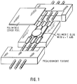
- Figure 1 shows a similar waveguide component.
- the fibers to be coupled are aligned beforehand (prealignment fixture).
- PMMA cover foils polymeric cover foils
- a core monomer adhesive is dripped into the waveguide depressions, pressed out with a film to a thickness of less than 1 ⁇ m and then cured by UV or thermal polymerization.
- the core polymer has an approximately 5 * 10 -3 higher refractive index and thus represents a dielectric waveguide with the surrounding polymer substrate.
- the length of these foils must be cut to an accuracy of approx. +/- 10 ⁇ m.
- the fibers to be coupled are placed in the V-grooves before the waveguide is bonded and glued to the substrate by the overflowing core monomer.
- the method with the measures according to claim 1 makes it possible that the processes of the fastener adjustment and the waveguide gluing do not have to be carried out at the same time as in the solutions according to the prior art.
- the core material on the substrate surface can be expressed to a thickness of less than 1 ⁇ m without the passive fiber adjustment being destroyed or disturbed.
- Foil covers to be cut to size, as in the example shown in FIG. 1, are unnecessary since the foil cover can be replaced by a molded microstructured cover component.
- the method according to the invention is suitable for both to be glued, d. H. covers remaining on the substrate component, as well as for strip-off covers.
- the lid components do not have to be cut manually with high precision, but instead automatically fit to the associated substrate component with a high precision to a few ⁇ m, since they come from the same mask.
- the essential, applied design idea is the possibility to be able to produce positive and negative forms using a triple-copy technique in nickel electroplating.
- Polymer substrates for waveguide components are manufactured, for example, with 6 * 6 ⁇ m waveguide grooves and effectively 67 ⁇ m deep fiber guide grooves, which have to be glued with a higher refractive index, polymeric core material for further processing.
- the core material on the substrate surface must be expressed to a thickness of less than 1 ⁇ m, but the passive fiber adjustment must not be disturbed or destroyed.
- the present invention describes a method for producing an integrated optical waveguide component with a particularly favorable waveguide bond.
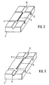
- FIG. 2 shows a silicon master structure and FIG. 3 shows a substrate component 1, which can represent both a passive (only waveguide grooves) and an active one (with embedded electro-optical components or heating electrodes).
- the waveguide structure area 3 can be seen, which is essentially transverse to the between two Fiber coupling areas - V-grooves 6 - arranged parallel grooves 4, 4 'extends.
- the master structure FIG. 2
- all structures, with the exception of the saw cuts, which represent the grooves 4, 4 ' are produced using an exposure mask and are therefore very precisely reproducible. Since the saw cut extends over the entire silicon wafer and there is practically no deviation from parallelism in the cutting direction, it can be assumed that the distance from the saw cut to the saw cut is always the same over the wafer.
- FIGS. 4 and 5 serve to explain the nickel electroplating copying technique.
- FIG. 4 shows 1st or 3rd generation nickel sheet obtained by electroplating, which can be used as cover component 2 without the webs in the waveguide structure area.
- the webs 5, 5 ' correspond to the grooves 4, 4' of the substrate component 1 and engage them in a precise fit when they are joined together.
- FIG. 5 shows a second generation nickel sheet from which a strip-off cover made of plastic can be molded.
- the invention is based on the knowledge that 1st, 2nd and 3rd generation nickel sheet are exact, better than ⁇ m accurate replicas, which differ only by a positive-negative conversion between two neighboring generations.
- FIG. 8 shows how, due to the geometric relationships described, a 3rd generation nickel sheet originating from the area AA 'snaps precisely into the saw cuts of the polymer substrate.
- the fiber guide grooves cannot be filled with core material, since the V-groove areas 6 of cover component 2 and substrate component are positive - negative identical copies that lie exactly on top of each other (webs 5, 5 '), especially with high mechanical pressure and a thin chrome plating Nickel strip-off cover in the V-groove area 6.
- the processes of waveguide formation in the structural area and the coupling of the fibers can thus be carried out at different times.
- a material of high optical transparency is used for the waveguide formation, whereas a material of high strength, in particular with regard to high temperature shock resistance, can be used for the coupling of the fibers.
- a disadvantage of the construction method described above i. is the permanent use of an expensive microstructured nickel sheet as a strip-off lid.
- incisions, holes, metallizations can be made on the microstructure cover etc. are not easily tested because the strip-off lid made of nickel is too valuable for risky modifications.
- the strip-off lid by plastic molding, z. B. by a thermoplastic impression, generated by a 2nd generation nickel, ie the molded plastic part is geometrically identical to a 3rd generation nickel strip-off cover, apart from changes in geometry due to different thermal expansion between metal and plastic, and can therefore be just like this be used if the plastic material has been correctly selected.
- Advantage of the construction process ii. is the possibility to produce almost any amount of strip-off lids by injection molding. In production, this gives you the option of using a separate cover component for each substrate component, so you do not need to clean the strip-off cover after each use. Chromium plating of the V-groove area with the aim of displacing the monomer from this area is like in method i. advantageous.
- the construction methods i. and ii. each produce a so-called strip-off waveguide, i.e. H. the waveguide core is initially unprotected on the surface of the polymer substrate and must therefore be protected with a polymer film in the next step.
- the third construction method iii. also uses a microstructure lid. However, this consists of a plastic that is glued by the core monomer, so that the cover can no longer be removed after the waveguide has been produced.
- the microstructure cover component 2 is molded from a mold insert that can be produced as follows: the starting point is a 2nd generation nickel sheet, which can be modified by fine mechanical rework. The V-groove area including the saw cut 4, 4 'is cut out from the associated 3rd generation nickel sheet. This part is reworked in such a way that its width just corresponds to the width of the fiber ribbon used later, i.e. z. B. for an eight-fiber ribbon 2 mm.
- the part is fitted into the V-groove area of the 2nd generation nickel sheet. Since both parts are inverse copies of each other, there is no gap in the saw cut of the 2nd generation nickel sheet (see Fig. 10). Then both parts are fixed by e.g. B. spot welding. Then the mold insert z. B. reworked by surface grinding so that ideally a 59.5 ⁇ m high step (Fig. 10). The molded from the mold insert, z. B. made of PMMA, press the fibers into the V-groove area of the substrate and at the same time close off the wave structure area 3 precisely, without a subsequent precise sawing as with conventional methods would be necessary.
- the negative-positive impression can also be taken in reverse order; d. H. as a starting form, a lid component is used, from which the substrate component is molded.
Landscapes
- Physics & Mathematics (AREA)
- General Physics & Mathematics (AREA)
- Optics & Photonics (AREA)
- Chemical & Material Sciences (AREA)
- Crystallography & Structural Chemistry (AREA)
- Optical Couplings Of Light Guides (AREA)
- Optical Integrated Circuits (AREA)
Abstract
Description
Die Erfindung geht aus von einem Verfahren zur Herstellung eines integriert optischen Wellenleiterbauteiles mit Faserankopplungen unter Verwendung eines Substratbauteiles, welches abgeformte Strukturen aufweist, und eines Deckelbauteiles, welches durch Abformung vom Substratbauteil gewonnen ist, sowie einer entsprechenden Anordnung.The invention is based on a method for producing an integrated optical waveguide component with fiber couplings using a substrate component which has molded structures and a cover component which is obtained by molding the substrate component, and a corresponding arrangement.
Aus der DE 42 17 553 A1 ist ein Wellenleiterbauteil bekannt, welches Faserankopplungen aufweist. Es besteht aus einem Basisteil aus polymeren Material und einem Deckelbauteil, welches als Negativform des Basisteiles aufgebaut ist. An den äußeren Enden sind V-nutförmige Faserankoppelbereiche vorgesehen. Im Mittelbereich des Basisteiles ist eine Wellenleitervertiefung vorgesehen, die mit einem optischen Wirkstoff, z. B. einem UV-aushärtenden Kleber versehen wird.DE 42 17 553 A1 discloses a waveguide component which has fiber couplings. It consists of a base part made of polymeric material and a cover component, which is constructed as a negative form of the base part. V-shaped fiber coupling areas are provided at the outer ends. In the central region of the base part, a waveguide recess is provided, which is coated with an optical active ingredient, e.g. B. is provided with a UV-curing adhesive.
Figur 1 zeigt ein ähnliches Wellenleiterbauteil. Die anzukoppelnden Fasern werden zuvor ausgerichtet (Prealignment Fixture). Für die Wellenleiterverklebung werden entweder PMMA-Abdeckfolien (Polymeric Cover Foil) verwendet, die nach Aushärten des Kernmonomers mit dem Substrat, das die Strukturen trägt, verklebt werden (Polymeric glue). Hierzu wird ein Kernmonomerkleber in die Wellenleitervertiefungen getropft, mit einer Folie auf unter 1 µm Dicke ausgedrückt und anschließend durch UV-oder thermische Polymerisation ausgehärtet. Nach der Polymerisation hat das Kernpolymer einen ca. 5*10-3 höheren Brechungsindex und stellt damit mit dem umgebenden Polymersubstrat einen dielektrischen Wellenleiter dar. Es können auch die unter dem Handelsnamen Mylar (TM) bekannten Folien verwendet werden, welche nach dem Aushärten des Kernmonomers abgezogen werden können (Strip-Off-Deckel). Diese Folien müssen auf der Länge auf ca. +/- 10 µm genau geschnitten werden. Wie in Figur 1 dargestellt, werden die anzukoppelnden Fasern vor der Wellenleiterverklebung in die V-Nuten eingelegt und durch das überlaufende Kernmonomer an das Substrat geklebt.Figure 1 shows a similar waveguide component. The fibers to be coupled are aligned beforehand (prealignment fixture). For the waveguide gluing either PMMA cover foils (polymeric cover foils) are used, which after hardening of the core monomer with the Substrate that carries the structures are glued (polymeric glue). For this purpose, a core monomer adhesive is dripped into the waveguide depressions, pressed out with a film to a thickness of less than 1 μm and then cured by UV or thermal polymerization. After the polymerization, the core polymer has an approximately 5 * 10 -3 higher refractive index and thus represents a dielectric waveguide with the surrounding polymer substrate. It is also possible to use the films known under the trade name Mylar (TM), which after the core monomer has hardened can be removed (strip-off lid). The length of these foils must be cut to an accuracy of approx. +/- 10 µm. As shown in FIG. 1, the fibers to be coupled are placed in the V-grooves before the waveguide is bonded and glued to the substrate by the overflowing core monomer.
Das Verfahren mit den Maßnahmen gemäß Patentanspruch 1 ermöglicht es , daß die Prozesse der Fasterjustage und der Wellenleiterverklebung nicht wie bei den Lösungen gemäß dem Stand der Technik zeitgleich durchgeführt werden müssen. Das Kernmaterial an der Substratoberfläche kann auf unter 1µm Dicke ausgedrückt werden, ohne daß die passive Faserjustage zerstört oder gestört wird.The method with the measures according to
Im Gegensatz zu den zuvor aufgezeigten Lösungen, bei denen die Stirnseiten der anzukoppelnden Glasfasern von demselben Monomer (Kernmonomer) verklebt werden, welches auch die Wellenleiterkerne bildet, können die Prozesse der Stirnseitenverklebung der Fasern (Faserjustage) von der Wellenleiterbildung zeitlich getrennt werden, wodurch sowohl die Faserjustierung und Faserfixierung als auch die Wellenleiterstrukturbildung verbessert werden kann. Auch können die Materialien hinsichtlich der unterschiedlichen Prozesse optimiert werden. Probleme hinsichtlich Temperaturwechselbelastung, wie sie sich bei den bekannten Lösungen, insbesondere durch Faserabriß manifestierten, können vermieden werden.In contrast to the solutions shown above, in which the end faces of the glass fibers to be coupled are glued by the same monomer (core monomer) that also forms the waveguide cores, the processes of gluing the end faces of the fibers (fiber adjustment) can be separated in time from the formation of the waveguide, whereby both Fiber adjustment and fixation as well as the waveguide structure formation can be improved. Also the materials can be optimized with regard to the different processes. Problems with regard to thermal cycling, as manifested in the known solutions, in particular through fiber tearing, can be avoided.
Zuzuschneidende Foliendeckel wie bei dem in Figur 1 dargestellten Beispiel sind entbehrlich, da der Foliendeckel durch ein abgeformtes mikrostrukturiertes Deckelbauteil ersetzt werden kann. Das Verfahren nach der Erfindung eignet sich sowohl für zu verklebende, d. h. auf dem Substratbauteil verbleibende Deckel, wie auch für Strip-Off-Deckel. Die Deckelbauteile müssen nicht manuell mit hoher Präzision zugeschnitten werden, sondern passen automatisch, da durch einen Abformprozeß von gleicher Maske stammend, auf wenige µm hochpräzise auf das zugehörige Substratbauteil. Die wesentliche, dabei angewandte Konstruktionsidee ist die Möglichkeit, über eine Dreifachumkopiertechnik in Nickelgalvanik Positiv- und Negativformen herstellen zu können.Foil covers to be cut to size, as in the example shown in FIG. 1, are unnecessary since the foil cover can be replaced by a molded microstructured cover component. The method according to the invention is suitable for both to be glued, d. H. covers remaining on the substrate component, as well as for strip-off covers. The lid components do not have to be cut manually with high precision, but instead automatically fit to the associated substrate component with a high precision to a few µm, since they come from the same mask. The essential, applied design idea is the possibility to be able to produce positive and negative forms using a triple-copy technique in nickel electroplating.
- Figur 2 zeigt eine Silizium-Masterstruktur für die Herstellung von Wellenleiterbauteilen nach der Erfindung,FIG. 2 shows a silicon master structure for the production of waveguide components according to the invention,
- Figur 3 zeigt ein zur Masterstruktur formgleiches Substratbauteil,FIG. 3 shows a substrate component of the same shape as the master structure,
- Figur 4 und Figur 5 zeigen Darstellungen zur Erläuterung der nickelgalvanischen Umkopiertechnik,FIG. 4 and FIG. 5 show illustrations for explaining the nickel electroplating copying technique,
- Figur 6 zeigt die Oberfläche eines Siliziumwafers für die Herstellung erfindungsgemäßer Wellenleiterbauteile,FIG. 6 shows the surface of a silicon wafer for the production of waveguide components according to the invention,
- Figur 7 zeigt Querschnitte durch die Silizium-Masterstruktur und durch das Substratbauteil,FIG. 7 shows cross sections through the silicon master structure and through the substrate component,
- Figur 8 zeigt das Einrasten eines Strip-Off-Deckelbauteiles in ein Polymersubstrat,FIG. 8 shows the engagement of a strip-off cover component in a polymer substrate,
- Figur 9 zeigt ein Kunststoff-Strip-Off-Deckelbauteil abgeformt von zweiter Generation Nickelblech undFigure 9 shows a plastic strip-off cover component molded from second generation nickel sheet and
- Figur 10 zeigt einen Formeinsatz zur Herstellung von mikrostrukturierten Deckelbauteilen, die auf dem Substratbauteil verbleiben.FIG. 10 shows a mold insert for the production of microstructured cover components which remain on the substrate component.
Polymersubstrate für Wellenleiterbauelemente werden beispielsweise mit 6*6 µm Wellenleiternuten und effektiv 67 µm tiefen Faserführungsnuten hergestellt, die zur Weiterverarbeitung mit einem höherbrechenden, polymeren Kernmaterial verklebt werden müssen. Damit ein monomodiger optischer Wellenleiter entsteht, muß das Kernmaterial an der Substratoberfläche auf unter 1µm Dicke ausgedrückt werden, wobei aber die passive Faserjustage nicht gestört bzw. zerstört werden darf. Die vorliegende Erfindung beschreibt ein Verfahren zur Herstellung eines integriert optischen Wellenleiterbauteiles mit einer besonders günstigen Wellenleiterverklebung.Polymer substrates for waveguide components are manufactured, for example, with 6 * 6 µm waveguide grooves and effectively 67 µm deep fiber guide grooves, which have to be glued with a higher refractive index, polymeric core material for further processing. In order for a single-mode optical waveguide to be formed, the core material on the substrate surface must be expressed to a thickness of less than 1 μm, but the passive fiber adjustment must not be disturbed or destroyed. The present invention describes a method for producing an integrated optical waveguide component with a particularly favorable waveguide bond.
Figur 2 zeigt eine Silizium-Masterstruktur und Figur 3 ein Substratbauteil 1, welches stellvertretend sowohl für ein passives (nur Wellenleiternuten) als auch ein aktives (mit eingebetteten elektrooptischen Bauteilen oder Heizelektroden) stehen kann. Neben den V-Nutbereichen 6 für die Faserankopplungen ist der Wellenleiterstrukturbereich 3 zu sehen, der sich zwischen zwei im wesentlichen quer zu den Faserankopplungsbereichen - V-Nuten 6 - angeordneten parallelen Nuten 4, 4' erstreckt. Auf der Masterstruktur (Fig. 2) sind alle Strukturen mit Ausnahme der Sägeschnitte, die die Nuten 4, 4' darstellen, über eine Belichtungsmaske erzeugt und damit sehr genau reproduzierbar. Da der Sägeschnitt über den gesamten Silizium-Wafer hinwegführt und in Schnittrichtung praktisch keine Abweichung von der Parallelität aufweist, kann davon ausgegangen werden, daß der Abstand von Sägeschnitt zu Sägeschnitt über den Wafer immer gleich ist.FIG. 2 shows a silicon master structure and FIG. 3 shows a
Die Figuren 4 und 5 dienen zur Erläuterung der nickelgalvanischen Umkopiertechnik. Figur 4 zeigt durch galvanische Abformung gewonnenes 1. bzw. 3. Generation Nickelblech, welches ohne die Stege im Wellenleiterstrukturbereich als Deckelbauteil 2 verwendbar ist. Die Stege 5, 5' entsprechen den Nuten 4, 4' des Substratbauteiles 1 und greifen in diese beim Zusammenfügen paßgenau ein.FIGS. 4 and 5 serve to explain the nickel electroplating copying technique. FIG. 4 shows 1st or 3rd generation nickel sheet obtained by electroplating, which can be used as
Figur 5 zeigt ein 2. Generation-Nickelblech aus dem ein Strip-Off-Deckel aus Kunststoff abgeformt werden kann.FIG. 5 shows a second generation nickel sheet from which a strip-off cover made of plastic can be molded.
Die Erfindung ermöglicht drei verschiedene Konstruktionsverfahren zur Herstellung mikrostrukturierter Deckelbauteile, die alle drei auf dem gleichen Konzept beruhen:
- i. Mikrostrukturierte Strip-Off-Deckel in einem 1. oder 3. Generation Nickelblech,
- ii. Mikrostrukturierte Strip-Off-Deckel aus Kunststoff, abgeformt von einem 2. Generation Nickelblech,
- iii. Mikrostrukturierte, am Substrat verbleibender Deckel aus Kunststoff, abgeformt von einem feinmechanisch nachgearbeiteten 2. Generation Nickelblech.
- i. Micro-structured strip-off lids in a 1st or 3rd generation nickel sheet,
- ii. Micro-structured strip-off lid made of plastic, molded from a 2nd generation nickel sheet,
- iii. Micro-structured plastic lid that remains on the substrate, molded from a precision-machined 2nd generation nickel sheet.
Die Erfindung basiert auf der Erkenntnis, daß 1., 2. und 3. Generation Nickelblech zueinander exakte, besser als µm genaue Replikate sind, die sich nur durch eine Positiv-Negativwandlung zwischen zwei benachbarten Generationen unterscheiden.The invention is based on the knowledge that 1st, 2nd and 3rd generation nickel sheet are exact, better than µm accurate replicas, which differ only by a positive-negative conversion between two neighboring generations.
Figur 6 zeigt einen strukturierten Silizium-Wafer mit folgenden Eigenschaften:
- 1) in allen vier sichtbaren Kavitäten (Bereiche auf einem Wafer, in dem ein Substrat oder ein Deckelbauteil enthalten ist) sind die sog. V-Nutbereiche (oberhalb und unterhalb der Sägeschnitte) sowie die Tieferlegungen (der Bereich einer Kavität liegt gegenüber der Silizium-Oberfläche auf einem ca. 200 µm hohem Mesa, genannt Tieferlegung", weil in 1.

oder 3. Generation Nickel die Mikrostruktur unter der Oberfläche liegt) identisch, da sie durch eine elektronisch erzeugte Maske und identische Prozeßschritte erzeugt wurden. - 2) In den beiden inneren Kavitäten, z. B. Schnitt B, B', befinden sich Wellenleiternuten, in den beiden äußeren Kavitäten, z. B. Schnitt A, A' befinden sich keine Wellenleiternuten.
- 3) Die beiden Sägeschnitte verlaufen über den gesamten Wafer nahezu perfekt parallel, wenn auch ihr Abstand zueinander nicht genau definiert ist (Toleranz ist abhängig von der Qualität der Wafersäge.
- 1) in all four visible cavities (areas on a wafer in which a substrate or a lid component is contained) are the so-called V-groove areas (above and below the saw cuts) as well as the lowering (the area of a cavity lies opposite the silicon Surface on an approx. 200 µm high mesa Lowering ", because in the 1st or 3rd generation nickel the microstructure is below the surface) identical, since they were generated by an electronically generated mask and identical process steps.
- 2) In the two inner cavities, e.g. B. section B, B ', there are waveguide grooves in the two outer cavities, for. B. Section A, A 'there are no waveguide grooves.
- 3) The two saw cuts run almost perfectly parallel over the entire wafer, even if their distance from one another is not precisely defined (tolerance depends on the quality of the wafer saw.
In Figur 7 sieht man die Konsequenz aus der oben unter 3. genannten Eigenschaft: die Länge ![]()
![]()
Figur 8 zeigt, wie aufgrund der geschilderten Geometrieverhältnisse ein aus dem Bereich AA' stammendes 3. Generation Nickelblech präzise in die Sägeschnitte des Polymersubstrates einrastet. Füllt man vor dem Zusammensetzen Kernmaterial (Kernmonomerkleber) zwischen Strip-Off-Deckel und Substrat und polymerisiert nach dem Zusammensetzen dieses Kernmaterial, z. B. durch Wärmezufuhr, aus, so entsteht bei richtiger Indexauswahl des Kernmaterials ein von Sägeschnitt 4 zu Sägeschnitt 4' reichender Wellenleiter. Der Strip-Off-Deckel läßt dabei die Wellenleitergräben frei. Die Faserführungsnuten können nicht von Kernmaterial gefüllt werden, da die V-Nut Bereiche 6 von Deckelbauteil 2 und Substratbauteil positiv - negativ identische Kopien sind, die exakt formschlüssig (Stege 5, 5') aufeinanderliegen, insbesondere bei hohem mechanischem Druck und einer dünnen Verchromung des Nickel-Strip-Off-Deckels im V-Nutbereich 6.FIG. 8 shows how, due to the geometric relationships described, a 3rd generation nickel sheet originating from the area AA 'snaps precisely into the saw cuts of the polymer substrate. Before assembling, core material (core monomer adhesive) is filled between the strip-off lid and the substrate and polymerized after assembling this core material, e.g. B. by the supply of heat, so arises with the correct index selection of the core material from saw cut 4 to saw cut 4 'reaching waveguide. The strip-off cover leaves the waveguide trenches free. The fiber guide grooves cannot be filled with core material, since the V-
Die Prozesse der Wellenleiterbildung im Strukturbereich und der Ankopplung der Fasern können dadurch zeitlich getrennt voneinander vorgenommen werden. Für die Wellenleiterbildung wird ein Material hoher optischer Transparenz eingesetzt, wohingegen für die Ankopplung der Fasern ein Material hoher Festigkeit, insbesondere hinsichtlich hoher Temperaturschockfestigkeit, einsetzbar ist.The processes of waveguide formation in the structural area and the coupling of the fibers can thus be carried out at different times. A material of high optical transparency is used for the waveguide formation, whereas a material of high strength, in particular with regard to high temperature shock resistance, can be used for the coupling of the fibers.
Nachteilig zu dem zuvor geschilderten Konstruktionsverfahren i. ist die Dauerverwendung eines teueren mikrostrukturierten Nickelbleches als Strip-Off-Deckel. Insbesondere können am Mikrostrukturdeckel Einschnitte, Löcher, Metallisierungen usw. nicht ohne weiteres getestet werden, weil der Strip-Off-Deckel aus Nickel zu wertvoll für risikobehaftete Modifikationen ist. Beim Konstruktionsverfahren ii. wie in Figur 9 dargestellt, wird der Strip-Off-Deckel durch Kunststoffabformung, z. B. durch eine thermoplastische Abformung, von einem 2. Generation Nickel erzeugt, d. h. das abgeformte Kunststoffteil ist abgesehen von Geometrieveränderungen durch unterschiedliche thermische Ausdehnung zwischen Metall und Kunststoff geometrisch identisch mit einem 3. Generation Nickel Strip-Off-Deckel und kann folglich genauso wie dieser eingesetzt werden, wenn der Kunststoffwerkstoff richtig ausgewählt wurde.A disadvantage of the construction method described above i. is the permanent use of an expensive microstructured nickel sheet as a strip-off lid. In particular, incisions, holes, metallizations can be made on the microstructure cover etc. are not easily tested because the strip-off lid made of nickel is too valuable for risky modifications. In the construction process ii. As shown in Figure 9, the strip-off lid by plastic molding, z. B. by a thermoplastic impression, generated by a 2nd generation nickel, ie the molded plastic part is geometrically identical to a 3rd generation nickel strip-off cover, apart from changes in geometry due to different thermal expansion between metal and plastic, and can therefore be just like this be used if the plastic material has been correctly selected.
Vorteilhaft an dem Konstruktionsverfahren ii. ist die Möglichkeit, eine nahezu beliebige Menge von Strip-Off-Deckeln im Spritzguß herzustellen. Man hat in der Fertigung damit die Möglichkeit, für jedes Substratbauteil ein eigenes Deckelbauteil zu verwenden und braucht den Strip-Off-Deckel somit nicht nach jedem Einsatz zu reinigen. Eine Verchromung des V-Nutbereiches mit dem Ziel, das Monomer aus diesem Bereich zu verdrängen, ist wie beim Verfahren i. vorteilhaft.Advantage of the construction process ii. is the possibility to produce almost any amount of strip-off lids by injection molding. In production, this gives you the option of using a separate cover component for each substrate component, so you do not need to clean the strip-off cover after each use. Chromium plating of the V-groove area with the aim of displacing the monomer from this area is like in method i. advantageous.
Die Konstruktionsverfahren i. und ii. erzeugen jeweils einen sog. Strip-Off-Wellenleiter, d. h. der Wellenleiterkern liegt zunächst ungeschützt an der Oberfläche des Polymersubstrates und muß daher im nächsten Arbeitsschritt mit einem Polymerfilm geschützt werden.The construction methods i. and ii. each produce a so-called strip-off waveguide, i.e. H. the waveguide core is initially unprotected on the surface of the polymer substrate and must therefore be protected with a polymer film in the next step.
Das dritte Konstruktionsverfahren iii. (dargestellt in Fig. 10) verwendet ebenfalls einen Mikrostrukturdeckel. Dieser besteht jedoch aus einem Kunststoff, der durch das Kernmonomer verklebt wird, sodaß der Deckel nach der Wellenleiterherstellung nicht mehr abnehmbar ist. Das Mikrostrukturdeckelbauteil 2 wird hier von einem Formeinsatz abgeformt, der wie folgt herstellbar ist: Ausgangspunkt ist ein 2. Generation Nickelblech, welches durch feinmechanische Nacharbeit zu modifizieren ist. Aus dem zugehörigen 3. Generation Nickelblech wird der V-Nutbereich inklusive des Sägeschnittes 4, 4' ausgeschnitten. Dieses Teil wird nachgearbeitet, derart, daß seine Breite gerade der Breite des später verwendeten Faserbändchens entspricht, also z. B. für ein Achtfaserbändchen 2 mm. Das Teil wird in den V-Nutbereich des 2. Generation Nickelbleches eingepaßt. Da beide Teile inverse Kopien voneinander sind, verbleibt im Sägeschnitt des 2. Generation Nickelbleches kein Spalt (siehe Fig. 10). Anschließend erfolgt die Fixierung beider Teile durch z. B. Punktschweißen. Dann wird der Formeinsatz z. B. durch Flächenschleifen so nachgearbeitet, daß idealerweise eine 59,5 µm hohe Stufe (Fig. 10) entsteht. Die von dem Formeinsatz abgeformten Deckel, z. B. aus PMMA, drücken die Fasern in den V-Nutbereich des Substrates und schließen gleichzeitig den Wellenstrukturbereich 3 präzise ab, ohne daß ein nachträgliches präzises Zusägen wie bei herkömmlichen Methoden notwendig wäre.The third construction method iii. (shown in Fig. 10) also uses a microstructure lid. However, this consists of a plastic that is glued by the core monomer, so that the cover can no longer be removed after the waveguide has been produced. The
Die Negativ-Positiv Abformung kann natürlich auch in umgekehrter Reihenfolge erfolgen; d. h. als Ausgangsform wird ein Deckelbauteil herangezogen, von welchem das Substratbauteil abgeformt wird.Of course, the negative-positive impression can also be taken in reverse order; d. H. as a starting form, a lid component is used, from which the substrate component is molded.
Claims (16)
Applications Claiming Priority (2)
| Application Number | Priority Date | Filing Date | Title |
|---|---|---|---|
| DE19619353 | 1996-05-14 | ||
| DE19619353A DE19619353A1 (en) | 1996-05-14 | 1996-05-14 | Method for producing an integrated optical waveguide component and arrangement |
Publications (2)
| Publication Number | Publication Date |
|---|---|
| EP0807836A2 true EP0807836A2 (en) | 1997-11-19 |
| EP0807836A3 EP0807836A3 (en) | 1997-12-17 |
Family
ID=7794244
Family Applications (1)
| Application Number | Title | Priority Date | Filing Date |
|---|---|---|---|
| EP97103691A Withdrawn EP0807836A3 (en) | 1996-05-14 | 1997-03-06 | Method of producing an integrated optical waveguide component and arrangement |
Country Status (3)
| Country | Link |
|---|---|
| US (1) | US5867619A (en) |
| EP (1) | EP0807836A3 (en) |
| DE (1) | DE19619353A1 (en) |
Cited By (27)
| Publication number | Priority date | Publication date | Assignee | Title |
|---|---|---|---|---|
| EP1645633A2 (en) | 2004-10-05 | 2006-04-12 | SunGene GmbH | Constitutive expression cassettes for regulation of plant expression |
| EP1655364A2 (en) | 2004-11-05 | 2006-05-10 | BASF Plant Science GmbH | Expression cassettes for seed-preferential expression in plants |
| EP1662000A2 (en) | 2004-11-25 | 2006-05-31 | SunGene GmbH | Expression cassettes for guard cell-preferential expression in plants |
| EP1666599A2 (en) | 2004-12-04 | 2006-06-07 | SunGene GmbH | Expression cassettes for mesophyll- and/or epidermis-preferential expression in plants |
| EP1669455A2 (en) | 2004-12-08 | 2006-06-14 | SunGene GmbH | Expression cassettes for vascular tissue-preferential expression in plants |
| EP1669456A2 (en) | 2004-12-11 | 2006-06-14 | SunGene GmbH | Expression cassettes for meristem-preferential expression in plants |
| WO2006089950A2 (en) | 2005-02-26 | 2006-08-31 | Basf Plant Science Gmbh | Expression cassettes for seed-preferential expression in plants |
| WO2006111512A1 (en) | 2005-04-19 | 2006-10-26 | Basf Plant Science Gmbh | Improved methods controlling gene expression |
| WO2006120197A2 (en) | 2005-05-10 | 2006-11-16 | Basf Plant Science Gmbh | Expression cassettes for seed-preferential expression in plants |
| WO2006133983A1 (en) | 2005-04-19 | 2006-12-21 | Basf Plant Science Gmbh | Starchy-endosperm and/or germinating embryo-specific expression in mono-cotyledonous plants |
| WO2008099013A1 (en) | 2007-02-16 | 2008-08-21 | Basf Plant Science Gmbh | Nucleic acid sequences for regulation of embryo-specific expression in monocotyledonous plants |
| EP2036984A2 (en) | 2002-07-26 | 2009-03-18 | BASF Plant Science GmbH | Reversion of the negative selective effect of negative marker proteins as selection procedure |
| EP2045327A2 (en) | 2005-03-08 | 2009-04-08 | BASF Plant Science GmbH | Expression enhancing intron sequences |
| EP2159289A2 (en) | 2005-06-23 | 2010-03-03 | BASF Plant Science GmbH | Improved methods for the production of stably transformed plants |
| EP2163635A1 (en) | 2004-08-02 | 2010-03-17 | BASF Plant Science GmbH | Method for isolation of transcription termination sequences |
| EP2186903A2 (en) | 2005-02-09 | 2010-05-19 | BASF Plant Science GmbH | Expression cassettes for regulation of expression in monocotyledonous plants |
| WO2011003901A1 (en) | 2009-07-10 | 2011-01-13 | Basf Plant Science Company Gmbh | Expression cassettes for endosperm-specific expression in plants |
| EP2275564A1 (en) | 2009-07-17 | 2011-01-19 | Freie Universität Berlin | Means and method for the production of transgenic plants that are resistant to clubroot |
| WO2011064736A1 (en) | 2009-11-27 | 2011-06-03 | Basf Plant Science Company Gmbh | Optimized endonucleases and uses thereof |
| WO2011064750A1 (en) | 2009-11-27 | 2011-06-03 | Basf Plant Science Company Gmbh | Chimeric endonucleases and uses thereof |
| WO2011067712A1 (en) | 2009-12-03 | 2011-06-09 | Basf Plant Science Company Gmbh | Expression cassettes for embryo-specific expression in plants |
| US8022272B2 (en) | 2001-07-13 | 2011-09-20 | Sungene Gmbh & Co. Kgaa | Expression cassettes for transgenic expression of nucleic acids |
| DE112010004584T5 (en) | 2009-11-27 | 2012-11-29 | Basf Plant Science Company Gmbh | Chimeric endonucleases and applications thereof |
| EP2612918A1 (en) | 2012-01-06 | 2013-07-10 | BASF Plant Science Company GmbH | In planta recombination |
| EP2980220A1 (en) | 2005-09-20 | 2016-02-03 | BASF Plant Science GmbH | Improved methods controlling gene expression |
| WO2021122081A1 (en) | 2019-12-16 | 2021-06-24 | Basf Se | Precise introduction of dna or mutations into the genome of wheat |
| WO2021122080A1 (en) | 2019-12-16 | 2021-06-24 | BASF Agricultural Solutions Seed US LLC | Improved genome editing using paired nickases |
Families Citing this family (10)
| Publication number | Priority date | Publication date | Assignee | Title |
|---|---|---|---|---|
| DE19842694A1 (en) * | 1998-09-17 | 2000-04-20 | Harting Elektrooptische Bauteile Gmbh & Co Kg | Microstructured body and process for its production |
| US6304695B1 (en) | 1999-05-17 | 2001-10-16 | Chiaro Networks Ltd. | Modulated light source |
| US6366720B1 (en) | 1999-07-09 | 2002-04-02 | Chiaro Networks Ltd. | Integrated optics beam deflector assemblies utilizing side mounting blocks for precise alignment |
| GB9919847D0 (en) * | 1999-08-20 | 1999-10-27 | British Telecomm | Alignment device |
| US7068870B2 (en) * | 2000-10-26 | 2006-06-27 | Shipley Company, L.L.C. | Variable width waveguide for mode-matching and method for making |
| US6813023B2 (en) | 2002-01-03 | 2004-11-02 | Chiaro Nerwork Ltd. | Automatic optical inter-alignment of two linear arrangements |
| US6886994B2 (en) * | 2002-07-18 | 2005-05-03 | Chiaro Networks Ltd. | Optical assembly and method for manufacture thereof |
| US6808322B2 (en) * | 2002-09-24 | 2004-10-26 | Triquint Technology Holding Co. | Devices and method of mounting |
| KR100476317B1 (en) * | 2002-10-24 | 2005-03-16 | 한국전자통신연구원 | Optical coupling device and method for fabricating the same, master for fabricating the optical coupling device and method for fabricating the same |
| CN107144919A (en) * | 2017-06-28 | 2017-09-08 | 湖北工业大学 | A kind of preparation method of polymer optical wave guide chip |
Citations (4)
| Publication number | Priority date | Publication date | Assignee | Title |
|---|---|---|---|---|
| WO1993021550A1 (en) * | 1992-04-10 | 1993-10-28 | Robert Bosch Gmbh | Process for producing optical polymer components with integral fibre/chip coupling by moulding |
| EP0589268A1 (en) * | 1992-09-17 | 1994-03-30 | Robert Bosch Gmbh | Integrated optical circuit with a Bragg structure |
| EP0608566A2 (en) * | 1992-12-28 | 1994-08-03 | Matsushita Electric Industrial Co., Ltd. | Opitcal component mounting substrate and method of producing the same |
| US5343544A (en) * | 1993-07-02 | 1994-08-30 | Minnesota Mining And Manufacturing Company | Integrated optical fiber coupler and method of making same |
Family Cites Families (4)
| Publication number | Priority date | Publication date | Assignee | Title |
|---|---|---|---|---|
| US4639074A (en) * | 1984-06-18 | 1987-01-27 | At&T Bell Laboratories | Fiber-waveguide self alignment coupler |
| FR2661516B1 (en) * | 1990-04-27 | 1992-06-12 | Alcatel Fibres Optiques | INTEGRATED OPTICAL COMPONENT AND MANUFACTURING METHOD. |
| FR2692684B1 (en) * | 1992-06-19 | 1997-04-04 | Corning Inc | OPTICAL COMPONENT CONNECTED TO AN OPTICAL FIBER NETWORK. |
| US5600745A (en) * | 1996-02-08 | 1997-02-04 | Industrial Technology Research Institute | Method of automatically coupling between a fiber and an optical waveguide |
-
1996
- 1996-05-14 DE DE19619353A patent/DE19619353A1/en not_active Withdrawn
-
1997
- 1997-03-06 EP EP97103691A patent/EP0807836A3/en not_active Withdrawn
- 1997-05-12 US US08/854,860 patent/US5867619A/en not_active Expired - Fee Related
Patent Citations (4)
| Publication number | Priority date | Publication date | Assignee | Title |
|---|---|---|---|---|
| WO1993021550A1 (en) * | 1992-04-10 | 1993-10-28 | Robert Bosch Gmbh | Process for producing optical polymer components with integral fibre/chip coupling by moulding |
| EP0589268A1 (en) * | 1992-09-17 | 1994-03-30 | Robert Bosch Gmbh | Integrated optical circuit with a Bragg structure |
| EP0608566A2 (en) * | 1992-12-28 | 1994-08-03 | Matsushita Electric Industrial Co., Ltd. | Opitcal component mounting substrate and method of producing the same |
| US5343544A (en) * | 1993-07-02 | 1994-08-30 | Minnesota Mining And Manufacturing Company | Integrated optical fiber coupler and method of making same |
Cited By (43)
| Publication number | Priority date | Publication date | Assignee | Title |
|---|---|---|---|---|
| US8022272B2 (en) | 2001-07-13 | 2011-09-20 | Sungene Gmbh & Co. Kgaa | Expression cassettes for transgenic expression of nucleic acids |
| US8604278B2 (en) | 2001-07-13 | 2013-12-10 | Sungene Gmbh & Co. Kgaa | Expression cassettes for transgenic expression of nucleic acids |
| EP2036984A2 (en) | 2002-07-26 | 2009-03-18 | BASF Plant Science GmbH | Reversion of the negative selective effect of negative marker proteins as selection procedure |
| EP2166103A1 (en) | 2004-08-02 | 2010-03-24 | BASF Plant Science GmbH | Method for isolation of transcription termination sequences |
| EP2166104A1 (en) | 2004-08-02 | 2010-03-24 | BASF Plant Science GmbH | Method for isolation of transcription termination sequences |
| EP2163635A1 (en) | 2004-08-02 | 2010-03-17 | BASF Plant Science GmbH | Method for isolation of transcription termination sequences |
| EP2166097A1 (en) | 2004-10-05 | 2010-03-24 | SunGene GmbH | Constitutive expression cassettes for regulation of plant expression |
| EP2166098A1 (en) | 2004-10-05 | 2010-03-24 | SunGene GmbH | Constitutive expression cassettes for regulation of plant expression |
| EP1645633A2 (en) | 2004-10-05 | 2006-04-12 | SunGene GmbH | Constitutive expression cassettes for regulation of plant expression |
| EP1655364A2 (en) | 2004-11-05 | 2006-05-10 | BASF Plant Science GmbH | Expression cassettes for seed-preferential expression in plants |
| EP2163631A1 (en) | 2004-11-25 | 2010-03-17 | SunGene GmbH | Expression cassettes for guard cell-preferential expression in plants |
| EP1662000A2 (en) | 2004-11-25 | 2006-05-31 | SunGene GmbH | Expression cassettes for guard cell-preferential expression in plants |
| EP1666599A2 (en) | 2004-12-04 | 2006-06-07 | SunGene GmbH | Expression cassettes for mesophyll- and/or epidermis-preferential expression in plants |
| EP2072620A2 (en) | 2004-12-08 | 2009-06-24 | SunGene GmbH | Expression casstettes for vascular tissue-preferential expression in plants |
| EP1669455A2 (en) | 2004-12-08 | 2006-06-14 | SunGene GmbH | Expression cassettes for vascular tissue-preferential expression in plants |
| EP1669456A2 (en) | 2004-12-11 | 2006-06-14 | SunGene GmbH | Expression cassettes for meristem-preferential expression in plants |
| EP2186903A2 (en) | 2005-02-09 | 2010-05-19 | BASF Plant Science GmbH | Expression cassettes for regulation of expression in monocotyledonous plants |
| WO2006089950A2 (en) | 2005-02-26 | 2006-08-31 | Basf Plant Science Gmbh | Expression cassettes for seed-preferential expression in plants |
| EP2045327A2 (en) | 2005-03-08 | 2009-04-08 | BASF Plant Science GmbH | Expression enhancing intron sequences |
| EP2166100A2 (en) | 2005-03-08 | 2010-03-24 | BASF Plant Science GmbH | Expression enhancing intron sequences |
| EP2166102A2 (en) | 2005-03-08 | 2010-03-24 | BASF Plant Science GmbH | Expression enhancing intron sequences |
| EP2166099A2 (en) | 2005-03-08 | 2010-03-24 | BASF Plant Science GmbH | Expression enhancing intron sequences |
| EP2166101A2 (en) | 2005-03-08 | 2010-03-24 | BASF Plant Science GmbH | Expression enhancing intron sequences |
| EP2169058A2 (en) | 2005-03-08 | 2010-03-31 | BASF Plant Science GmbH | Expression enhancing intron sequences |
| WO2006111512A1 (en) | 2005-04-19 | 2006-10-26 | Basf Plant Science Gmbh | Improved methods controlling gene expression |
| WO2006133983A1 (en) | 2005-04-19 | 2006-12-21 | Basf Plant Science Gmbh | Starchy-endosperm and/or germinating embryo-specific expression in mono-cotyledonous plants |
| WO2006120197A2 (en) | 2005-05-10 | 2006-11-16 | Basf Plant Science Gmbh | Expression cassettes for seed-preferential expression in plants |
| EP2159289A2 (en) | 2005-06-23 | 2010-03-03 | BASF Plant Science GmbH | Improved methods for the production of stably transformed plants |
| EP2980220A1 (en) | 2005-09-20 | 2016-02-03 | BASF Plant Science GmbH | Improved methods controlling gene expression |
| WO2008099013A1 (en) | 2007-02-16 | 2008-08-21 | Basf Plant Science Gmbh | Nucleic acid sequences for regulation of embryo-specific expression in monocotyledonous plants |
| WO2011003901A1 (en) | 2009-07-10 | 2011-01-13 | Basf Plant Science Company Gmbh | Expression cassettes for endosperm-specific expression in plants |
| EP2275564A1 (en) | 2009-07-17 | 2011-01-19 | Freie Universität Berlin | Means and method for the production of transgenic plants that are resistant to clubroot |
| DE112010004583T5 (en) | 2009-11-27 | 2012-10-18 | Basf Plant Science Company Gmbh | Chimeric endonucleases and applications thereof |
| WO2011064750A1 (en) | 2009-11-27 | 2011-06-03 | Basf Plant Science Company Gmbh | Chimeric endonucleases and uses thereof |
| DE112010004584T5 (en) | 2009-11-27 | 2012-11-29 | Basf Plant Science Company Gmbh | Chimeric endonucleases and applications thereof |
| DE112010004582T5 (en) | 2009-11-27 | 2012-11-29 | Basf Plant Science Company Gmbh | Optimized endonucleases and applications thereof |
| WO2011064736A1 (en) | 2009-11-27 | 2011-06-03 | Basf Plant Science Company Gmbh | Optimized endonucleases and uses thereof |
| WO2011067712A1 (en) | 2009-12-03 | 2011-06-09 | Basf Plant Science Company Gmbh | Expression cassettes for embryo-specific expression in plants |
| EP3002332A2 (en) | 2009-12-03 | 2016-04-06 | BASF Plant Science Company GmbH | Expression cassettes for embryo-specific expression in plants |
| EP2612918A1 (en) | 2012-01-06 | 2013-07-10 | BASF Plant Science Company GmbH | In planta recombination |
| WO2013102875A1 (en) | 2012-01-06 | 2013-07-11 | Basf Plant Science Company Gmbh | In planta recombination |
| WO2021122081A1 (en) | 2019-12-16 | 2021-06-24 | Basf Se | Precise introduction of dna or mutations into the genome of wheat |
| WO2021122080A1 (en) | 2019-12-16 | 2021-06-24 | BASF Agricultural Solutions Seed US LLC | Improved genome editing using paired nickases |
Also Published As
| Publication number | Publication date |
|---|---|
| DE19619353A1 (en) | 1997-11-20 |
| US5867619A (en) | 1999-02-02 |
| EP0807836A3 (en) | 1997-12-17 |
Similar Documents
| Publication | Publication Date | Title |
|---|---|---|
| EP0807836A2 (en) | Method of producing an integrated optical waveguide component and arrangement | |
| EP0560043B1 (en) | Manufacturing method of devices for lightguide networks and elements produced using this method | |
| EP0635139B1 (en) | Process for producing optical polymer components with integral fibre/chip coupling by moulding | |
| EP0622647A2 (en) | Optical waveguide having an essentially planar substrate and its application | |
| EP0429877B1 (en) | Device for positioning optical fibres in connector elements | |
| DE60309669T2 (en) | METHOD FOR PRODUCING AN OPTICAL DEVICE BY MEANS OF A REPLICATION PROCESS | |
| DE19607671A1 (en) | Process for the production of optical components with coupled optical waveguides and components produced by this process | |
| EP0445527A2 (en) | Optical waveguide component and method of manufacturing an optical waveguide component | |
| DE4401219A1 (en) | Integrated optical component and method for producing an integrated optical component | |
| DE4440981A1 (en) | Optical reflector, esp. e.g. a parabolic mirror | |
| DE4200397C1 (en) | ||
| DE3010971C2 (en) | ||
| DE4423842C2 (en) | Connector for optical fibers and mold insert for the production of the same | |
| EP0576999A1 (en) | Method and device to produce optical elements | |
| EP0589268B1 (en) | Integrated optical circuit with a Bragg structure | |
| WO1994028449A1 (en) | Process for producing guiding elements for optical waveguide fibres | |
| EP1005663B1 (en) | Method for producing an optical component integrated in the waveguide chip with plug-in connector | |
| EP1671167B1 (en) | Method for the production of electrooptical printed circuit boards comprising polysiloxane wave guides and use thereof | |
| DE19602736A1 (en) | Method and device for producing optical lenses and optical lens arrays | |
| DE3712145A1 (en) | Optical component of adjustable focal length | |
| DE4200396C1 (en) | ||
| DE3443693A1 (en) | Optical plug connection with centring arrangement, and method for the manufacture of such centring arrangements | |
| DE2926003A1 (en) | DEVICE AND METHOD FOR PRODUCING PARTS OF AN OPTICAL BRANCHING ELEMENT | |
| DE4441526C2 (en) | Process for the production of optical components | |
| DE3112887C2 (en) | Method for producing a coupling element for coupling light in and / or out |
Legal Events
| Date | Code | Title | Description |
|---|---|---|---|
| PUAI | Public reference made under article 153(3) epc to a published international application that has entered the european phase |
Free format text: ORIGINAL CODE: 0009012 |
|
| PUAL | Search report despatched |
Free format text: ORIGINAL CODE: 0009013 |
|
| AK | Designated contracting states |
Kind code of ref document: A2 Designated state(s): DE FR GB IT |
|
| AK | Designated contracting states |
Kind code of ref document: A3 Designated state(s): DE FR GB IT |
|
| 17P | Request for examination filed |
Effective date: 19980617 |
|
| RAP1 | Party data changed (applicant data changed or rights of an application transferred) |
Owner name: HARTING ELEKTRO-OPTISCHE BAUTEILE GMBH & CO. KG. |
|
| STAA | Information on the status of an ep patent application or granted ep patent |
Free format text: STATUS: THE APPLICATION IS DEEMED TO BE WITHDRAWN |
|
| 18D | Application deemed to be withdrawn |
Effective date: 20021001 |