EP0804323B1 - Arrangement for converting optical into electrical signals and process for producing it - Google Patents
Arrangement for converting optical into electrical signals and process for producing it Download PDFInfo
- Publication number
- EP0804323B1 EP0804323B1 EP96900267A EP96900267A EP0804323B1 EP 0804323 B1 EP0804323 B1 EP 0804323B1 EP 96900267 A EP96900267 A EP 96900267A EP 96900267 A EP96900267 A EP 96900267A EP 0804323 B1 EP0804323 B1 EP 0804323B1
- Authority
- EP
- European Patent Office
- Prior art keywords
- substrate
- optical fibre
- mirror
- arrangement
- stamping
- Prior art date
- Legal status (The legal status is an assumption and is not a legal conclusion. Google has not performed a legal analysis and makes no representation as to the accuracy of the status listed.)
- Expired - Lifetime
Links
Images


Classifications
-
- G—PHYSICS
- G02—OPTICS
- G02B—OPTICAL ELEMENTS, SYSTEMS OR APPARATUS
- G02B6/00—Light guides; Structural details of arrangements comprising light guides and other optical elements, e.g. couplings
- G02B6/24—Coupling light guides
- G02B6/42—Coupling light guides with opto-electronic elements
- G02B6/4201—Packages, e.g. shape, construction, internal or external details
- G02B6/4219—Mechanical fixtures for holding or positioning the elements relative to each other in the couplings; Alignment methods for the elements, e.g. measuring or observing methods especially used therefor
- G02B6/4228—Passive alignment, i.e. without a detection of the degree of coupling or the position of the elements
- G02B6/4232—Passive alignment, i.e. without a detection of the degree of coupling or the position of the elements using the surface tension of fluid solder to align the elements, e.g. solder bump techniques
-
- G—PHYSICS
- G02—OPTICS
- G02B—OPTICAL ELEMENTS, SYSTEMS OR APPARATUS
- G02B6/00—Light guides; Structural details of arrangements comprising light guides and other optical elements, e.g. couplings
- G02B6/24—Coupling light guides
- G02B6/42—Coupling light guides with opto-electronic elements
- G02B6/4201—Packages, e.g. shape, construction, internal or external details
- G02B6/4204—Packages, e.g. shape, construction, internal or external details the coupling comprising intermediate optical elements, e.g. lenses, holograms
- G02B6/4214—Packages, e.g. shape, construction, internal or external details the coupling comprising intermediate optical elements, e.g. lenses, holograms the intermediate optical element having redirecting reflective means, e.g. mirrors, prisms for deflecting the radiation from horizontal to down- or upward direction toward a device
-
- G—PHYSICS
- G02—OPTICS
- G02B—OPTICAL ELEMENTS, SYSTEMS OR APPARATUS
- G02B6/00—Light guides; Structural details of arrangements comprising light guides and other optical elements, e.g. couplings
- G02B6/24—Coupling light guides
- G02B6/36—Mechanical coupling means
- G02B6/3628—Mechanical coupling means for mounting fibres to supporting carriers
- G02B6/3684—Mechanical coupling means for mounting fibres to supporting carriers characterised by the manufacturing process of surface profiling of the supporting carrier
- G02B6/3692—Mechanical coupling means for mounting fibres to supporting carriers characterised by the manufacturing process of surface profiling of the supporting carrier with surface micromachining involving etching, e.g. wet or dry etching steps
-
- G—PHYSICS
- G02—OPTICS
- G02B—OPTICAL ELEMENTS, SYSTEMS OR APPARATUS
- G02B6/00—Light guides; Structural details of arrangements comprising light guides and other optical elements, e.g. couplings
- G02B6/24—Coupling light guides
- G02B6/36—Mechanical coupling means
- G02B6/3628—Mechanical coupling means for mounting fibres to supporting carriers
- G02B6/3684—Mechanical coupling means for mounting fibres to supporting carriers characterised by the manufacturing process of surface profiling of the supporting carrier
- G02B6/3696—Mechanical coupling means for mounting fibres to supporting carriers characterised by the manufacturing process of surface profiling of the supporting carrier by moulding, e.g. injection moulding, casting, embossing, stamping, stenciling, printing, or with metallic mould insert manufacturing using LIGA or MIGA techniques
Definitions
- the invention is based on a method and one Arrangement according to the type of independent claims 1 and 15.
- a known generic arrangement (DE-PS 41 06 721) is based on a silicon carrier. On one surface he has several made by anisotropic etching V-grooves, which by bevelled, mirrored End faces are completed. The V-grooves are used for Fixation of optical fibers that mirrored End faces for deflecting via the optical fiber transmitted light in a direction perpendicular to the optical Optical fiber axis.
- Located on the silicon substrate a second support made of translucent material, thereupon in turn transducer elements for converting optical ones into electrical signals.
- DE-OS 42 12 208 is also the proposal known to mold master structures in plastics, so an inexpensive mass production of polymer components with self-adjusting coupling from Fiber guidance structures on light wave components enable. Measures for training electrical This procedure does not provide for structures.
- a generic device is known from DE-A-3 543 558.
- the invention has for its object a method for a more economical production of a generic Arrangement and a producible according to the method Specify order.
- the impression technique elaborate mirror shapes such as focusing Parabolic mirrors or similar beam-shaping elements can be manufactured inexpensively.
- the mirror metallization can advantageously in one step with the electrode production.
- embossing is expediently carried out using an embossing process. Should be on the surface of the ceramic substrate created structures have particularly smooth surfaces, embossing is advantageously carried out in two stages. Before the second A smooth sintering material is embossed into the Microstructure filled in.
- An advantageous variant for producing particularly smooth Mirror surfaces provides for that for the mirror intended surface before embossing locally a smooth sintering Apply glass paste.
- the production of the ceramic substrate in an equally advantageous manner also in casting technology, Slip casting or injection molding technology or injection stamping technology respectively.
- An advantageous way to avoid the Sintering shrinkage provides that to be sintered Ceramic mold during sintering using one on the embossed foil press tool under pressure put. As a press tool, the can easily Embossing the ceramic substrate used mold be used.
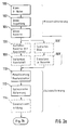
- FIG. 1 shows a proposed signal conversion arrangement in plan view and in longitudinal section
- Figure 2 a Flow chart of the proposed manufacturing process
- Figure 3 shows a detail of a mold
- Figure 4 shows a Cross section through an embossed V-groove before and after Sintering
- Figure 5 shows a longitudinal section through an embossed Microstructure with optical fiber to illustrate the Effects of shrinkage during sintering
- Figure 6 a Illustration of the use of a press tool in Sintering
- Figure 7 shows a transducer arrangement with an ellipsoidal mirror.
- the reflection preferably takes place at an angle of 90 degrees, the mirror 15 then has an inclination to the optical axis of the optical fiber 20 of 45 degrees.
- a receiver or a transmitter 22 and an RF (radio frequency) preamplifier 24 are arranged on the top 19 of the ceramic substrate 10. Both elements 22, 24 are preferably designed in the form of chips. They are connected to the ceramic substrate 10 via contact surfaces 29, which also serve for fixing. Transmitter / receiver chip 22 and RF preamplifier 24 are connected to one another via conductor tracks 26 which are also applied to the surface 19 of the ceramic substrate 10 and which are all or partially designed as strip conductors. Further strip conductors 26 ', applied directly to the ceramic substrate 10 in the same way, serve to integrate the entire transducer arrangement into the surrounding electronics.
- the transmitter / receiver chip 22 has a detection window 28 on its underside, ie on the side facing the substrate surface 19. It is located exactly above the beam spot, which generates the light transmitted via the optical fiber 20 and reflected on the mirror 15.
- the detection window 28 is generally a photodiode, which receives light transmitted via the optical fiber 20.
- the window 28 is, for example, a surface-emitting laser diode which feeds light into the optical fiber 20 via the mirror 15.
- An essential advantage of the arrangement shown in FIG. 1 is the use of a ceramic substrate 10. This means that additional insulation of the conductor tracks 26 and contact surfaces 25 from the surface 19 of the substrate 10 can be omitted. This in turn also allows the steps of mirror production and metallization of the conductor tracks or contact areas 25 to be combined.
- Figure 2 illustrates with the aid of a flow chart Sequence of a for producing an arrangement according to FIG. 1 appropriate procedure. It is divided into the sub-processes Microstructuring, electroforming, molding, Mirror production and metallization, as well as micro assembly.
- the first process sub-process is used to produce a Master structure for the impression. This is expediently done by known microtechnologies, for example in silicon micromechanics.
- a silicon waver in one first step 100 in a known manner, preferably by means of an anisotropic etching process in hot KOH solution, V-grooves 11 ', which will later be used as management structures for the Optical fibers 20 serve. Your depth can, as the Walls of the V-grooves along the (111-) crystal faces in the Always form silicon under a slope of 54.7 degrees, in simple way through the opening width of the Lithography mask can be determined.
- the experimental Accuracy is about 1 ⁇ m.
- step 102 one as Depression serving recess 13 etched. Your measurements depend on the diameter of the optical fiber 20 surrounding protective jacket 21. Am inside the silicon wafer 10 'lying end of the V-groove is then in step 104 trough-shaped cavern 12 'etched.
- FIG. 3 shows Illustration of the process flow a detail of a Master structure with V-groove 11 'and cavern 12'. In the structures for train interception, Fiber guidance and mirror in a single mask process defined and etched together.
- a practical one Possibility to create any inclination of the Mirror 15, for example 45 degrees, provides that Cavern 12 'initially with a contour material 16, in simple way to fill up a plastic, step 106, which is then stamped under the the desired angle of the ground cutting edge is formed, Step 108. Thereby possibly got into the V-groove 11 ' Plastic residues can be removed, for example, by laser ablation be selectively removed.
- Another, also useful Possibility to generate a mirror 15 with any Mirror surface provides the desired mirror contour For example, grind in a Pyrex glass and this in to insert the cavern 12 ', step 108'.
- the is fixed Glass bodies are expedient by direct bonding with the silicon.
- the prepared silicon master structure is metallized, Step 110, followed by electroplating a metal mold in a manner known per se produced.
- a metal mold in a manner known per se produced.
- This can be done by passivating the electroplating surface and then electroplating is grown on electroplating.
- the first mold insert the so-called mother, is created here an intermediate copy as the first generation, of which in turn by taking a second mold Generation. Since many interim copies of a mother and of each intermediate copy, many form inserts of the second Generation can be demolded inexpensively is one cost effective multiplication of molds easily possible.
- the impression with the help of Molding tools made of ceramic substrates 10 ', which The basis of the arrangement according to Figure 1 are.
- Cast ceramic green tapes are the starting material in foil form. They consist of compounds in particular fine-grained ceramic powder with organic binders, their Thicknesses typically range between 100 and 800 ⁇ m.
- the Impression molding process a pre-compression of the ceramic films by pressing. The measure will Structural fidelity improved in the later sintering process. To one sufficiently smooth surface of the later mirror 15 can then ensure on the for the mirror 15 intended area, i.e.
- one smooth sintered glass paste can be printed locally, step 118.
- step 120 the molding tool is moved to the in prepared steps 116 and 118 placed film.
- the film, and optionally also the molding tool, is now heated, step 122, then the mold is in embossed the film, step 124. This is followed by Cooling the film with constant holding pressure, step 130 as well as the demolding.
- Step 132 the embossed foils are compacted.
- Steps 116 through 130 may take the impression more advantageously Way also by casting (slip casting) of liquid ceramic slip on a molding tool, step 117. Of the Ceramic slip is then dried, step 119, demolded from the mold, step 121, and again sintered, step 132.
- the slip casting process draws is characterized by a very even material compression. This can cause uneven shrinkage in the subsequent Sintering process are largely prevented.
- an isotropic occurs during sintering Shrinkage typically around 20%.
- careful Control of the sintering process in step 132 i.e. in particular by closely monitoring the temperatures and the sintering time, as well as by appropriate coordination of Embossing parameters, powder quality and sintering parameters but is a reproducibility of the structure shown possible with an accuracy of ⁇ 1% of the shrinkage.
- shrinkage can occur during the manufacture of the Master structures are kept in the first sub-process.
- FIG. 4 illustrates the influence of shrinkage when sintering using the shrinkage of a V-groove.
- step 132 leads easily alongside Rounding of corners and edges, as in Figure 4 indicated.
- Sidewalls are adjusting while the trench tip the V-structure and the upper edges are not can have a determining effect on the problem of Rounding through a suitable design of the microstructures be counteracted well. This applies in particular to the mirror surfaces, because for the function of the mirror 15 as Deflection element also only the inclined surface essential is, but not the bounding edges.
- the main consequence of the shrinkage is, as in FIG. 5 shown, a height shift of the optical axis of the Optical fiber 20 by an amount ⁇ h.
- a height shift of the optical axis of the Optical fiber 20 by an amount ⁇ h is particularly easy.
- the effects of the shrinkage can be controlled, if, as assumed in Figure 5, a less than 45 degrees against the optical axis of the optical fiber inclined mirror 15 is used. This reflects over the optical fiber 20 transmitted light always vertically upwards.
- the through the beam spot caused by the light moves due to this the shrinkage by an amount ⁇ x in the direction of the optical Axis of the optical fiber 20, which with the Height shift ⁇ h of the optical fiber 20 matches.
- a pressing tool 23 is placed on the embossed ceramic substrate 10 during the sintering. It consists of a refractory material, for example of silicon nitride (Si 3 N 4 ) or aluminum oxide (Al 2 O 3 ) and is coated on the contact surface to the ceramic substrate 10 with a release agent 17. The latter can also be applied to the ceramic substrate 10.
- the surface of the pressing tool 23 corresponds to an exact negative impression of the embossed surface of the ceramic substrate 10. With the help of the pressing tool 10, a pressure P is now exerted on the ceramic substrate 10 during the sintering. If the pressure P is sufficient, shrinkage of the ceramic substrate 10 can be almost completely avoided, and the structures produced during embossing remain true to size.
- the pressing tool 23 is expediently designed to be slightly porous, so that the exhaust gases generated during the sintering fire through the Press tool 23 can escape.
- a release agent 17 is in usually required to press tool 23 and Ceramic substrate 10 from each other again after sintering to be able to separate.
- a single tool both as a molding tool for performing steps 117 or 124 as well as a pressing tool for use be provided in the manner described above. This is particularly useful if the impression is taken Ceramic slip casting according to steps 117 to 121 he follows.
- the mold can already be used a release agent 17 may be coated so that a Demolding, step 121 before sintering, step 132 can be omitted.
- step 124 also a two stage Embossing may be provided.
- the film is thereby in step 124 first embossed with reduced embossing pressure.
- the mold is raised and on smooth sintering material, preferably a Glass ceramic material, filled into the structure produced, Step 126. If necessary, the material is predried, Step 127. This is followed by a second embossing step, Step 128 the final impression.
- mirror smoothing in the form of a selective coating the surface provided for the mirror 15 take place to Example by spray coating, with a polymer film, such as such as photoresist, polyimide, or benzocyclobutene.
- a polymer film such as such as photoresist, polyimide, or benzocyclobutene.
- Such a Polymer film smoothes the coated surface directly or if necessary after melting once.
- Another smoothing of the Mirror surface can be created by glossy galvanic Strengthening of the metallization can be achieved.
- the electrical wiring which is usually a High frequency wiring in the form of coplanar Includes strip conductors, as well as the contact surfaces 29 (Contact pads) for connecting the electrical components 22, 24 applied.
- the metallization of the masking step is expedient Mirror surface.
- the mask is embossed on the Alignment marks 18 aligned, thus lateral shrinkage automatically taken into account in the position of the electrodes.
- the metallized ceramic substrate 10 is final populated, step 140.
- the transmitter / receiver chip 22 on the prepared one Contact surfaces 29 placed and connected to the substrate (bonded).
- About the melting solder balls on the Contact pads 29 is in a manner known per se Self-centering possible.
- an active adjustment of the transmitter / receiver chip with an optical Positioning device take place.
- Receiver diode with the detection zone up over the Mirrors 15 are mounted when the wafer material for the light wavelength to be received is transparent.
- the preamplifier tip 24 is applied in this manner. After that the optical fiber 20 is placed in the fiber-guiding V-groove 11, pushed under the chip 22 to the mirror 15 and fixed.
- the signals are usually transmitted via the converter arrangement described at a transmission rate of 5 to 11 gigabits / second.
- the active area of the diode 28 must therefore not exceed a diameter of approximately 50 ⁇ m in order to be able to keep the diode capacitances small.
- a smaller beam spot is created by filling a medium with a larger refractive index into the cavern 12 reached, step 140.
- the Beam spot by inserting an optical epoxy adhesive with a refractive index of typically n ⁇ 1.5 to about Reduce 20 ⁇ m. This is a high bit rate Receiver module possible without further beam focusing.
- the mirror 15 can for this purpose, for example, be designed as a concave mirror.
- While maintaining the underlying concepts is one Variety of configurations of the previously described Arrangement or the procedure possible. That's how it is Manufacturing process not based on a ceramic stamping technique limited. Rather, it is similarly expandable to others moldable materials such as thermoplastic Plastics, reaction casting resins, slip casting, sprayable Ceramic compounds or organically modified ceramics. Basically, the procedure is not based on that either Manufacture of electro-optical converter arrangements restricted, but also allows, for example, the Manufacture of micro-optical benches.
- fiber guides in the form of V-grooves Mounts for other micro-optical components, such as optical isolators, microlenses, filter pads, etc. embossed.
Landscapes
- Physics & Mathematics (AREA)
- General Physics & Mathematics (AREA)
- Optics & Photonics (AREA)
- Optical Couplings Of Light Guides (AREA)
- Mechanical Coupling Of Light Guides (AREA)
Abstract
Description
Die Erfindung geht aus von einem Verfahren und einer
Anordnung nach der Gattung der unabhängigen Ansprüche 1 und
15. Eine bekannte gattungsgemäße Anordnung (DE-PS 41 06 721)
basiert auf einem Träger aus Silizium. Auf einer Oberfläche
weist er mehrere, durch anisotropes Ätzen hergestellte
V-Nuten auf, welche durch abgeschrägte, verspiegelte
Stirnflächen abgeschlossen sind. Die V-Nuten dienen zur
Fixierung von Lichtleitfasern, die verspiegelten
Stirnflächen zur Umlenkung von über die Lichtleitfaser
übertragenem Licht in eine Richtung senkrecht zur optischen
Achse der Lichtleitfaser. Auf dem Siliziumträger befindet
sich ein zweiter Träger aus lichtdurchlässigem Material,
darauf wiederum Wandlerelemente zur Umwandlung von optischen
in elektrische Signale. Durch den lichtdurchlässigen zweiten
Träger wird letzteren das an den verspiegelten Stirnflächen
der V-Nuten umgelenkte Licht zugeführt. In ein
Siliziumsubstrat geätzte V-Nuten, wie sie bei dieser
bekannten Anordnung verwendet werden, stellen hervorragende
Faserführungsstrukturen dar. Auch sind die, entsprechend der
Siliziumkristallstruktur unter 54 Grad geneigten
Stirnflächen an den V-Nutenden, gut als Umlenkspiegel
nutzbar. Allerdings ist das Ätzen eines solchen Substrates
ein aufwendiges Herstellungsverfahren, da es einzeln
erfolgen muß. Technisch bedingt ferner die Hochfrequenz der
am Ausgang der Wandlereinrichtung anliegenden Signale, daß
die von der Wandlereinrichtung wegführenden Leiterbahnen als
elektrische Streifenleiter ausgeführt sind. Diese erfordern
stets eine hinreichend gute elektrische Isolation, indem
etwa zwischen Wandlereinrichtung mit Leiterbahnen und
Siliziumträger eine dielektrische Schicht, zum Beispiel
Polymid oder Glas, angeordnet wird. Aus technischen Gründen
ist es auch wünschenswert, die von der Wandlereinrichtung
gelieferten Signale auf einem möglichst kurzen Signalweg
einer Signalvorverarbeitung zuzuführen. Sie sollte daher
möglichst auf demselben Substrat unmittelbar an der
Wandlereinrichtung plaziert sein. Eine diesen technischen
Erfordernissen geügende Ausgestaltung des Substrates führt
allerdings zu einem vergleichsweise großen Platzbedarf für
jede Einzelanordnung, und damit zu einer Herabsetzung der
möglichen Integrationsdichte der mechanischen
Führungsstrukturen auf den Substraten. Es können dadurch aus
einem Siliziumwafer jeweils nur verhältnismäßig wenige
Einzelanordnungen gefertigt werden, wodurch sich
entsprechend erhöhte Herstellungskosten ergeben.The invention is based on a method and one
Arrangement according to the type of
Aus der DE-PS 43 00 652 ist der Vorschlag bekannt, eine integrierte optische Schaltung durch Eingießen eines elektrooptischen Halbleiterbauelementes auf einem Abformwerkzeug herzustellen. Als für das Gießen geeignetes Material sind Kunststoffe, insbesondere Polymere, offenbart.From DE-PS 43 00 652 the proposal is known, one integrated optical circuit by pouring one electro-optical semiconductor device on a Manufacture impression tool. As suitable for casting Material, plastics, in particular polymers, are disclosed.
Das Verfahren sieht eine Trennung von Substratherstellung und Mikromontage nicht vor. Eine kontrollierte Ausbildung von elektrischen und optischen Funktionsstrukturen auf der Substratoberfläche ist deshalb nicht möglich.The process sees a separation of substrate production and micro assembly not before. Controlled training of electrical and optical functional structures on the The substrate surface is therefore not possible.
Aus der DE-OS 42 12 208 ist desweiteren der Vorschlag bekannt, Master-Strukturen in Kunststoffe abzuformen, um so eine kostengünstige Massenproduktion von Polymerbauelementen mit selbstjustierender Ankopplung von Faserführungsstrukturen an Lichtwellenbauelemente zu ermöglichen. Maßnahmen zur Ausbildung von elektrischen Strukturen sieht dieses Verfahren nicht vor.DE-OS 42 12 208 is also the proposal known to mold master structures in plastics, so an inexpensive mass production of polymer components with self-adjusting coupling from Fiber guidance structures on light wave components enable. Measures for training electrical This procedure does not provide for structures.
Aus der DE-OS 43 17 953 ist ferner der Vorschlag entnehmbar, Führungsnuten für Glasfasern in Lichtwellenleiterführungselementen durch Spritzgießen in Kunststoff unter Verwendung eines Abformteiles herzustellen. Angaben zur Vorbereitung der dabei hergestellten Formteile für eine nachfolgende Montage von elektrischen Bauelementen macht die Schrift nicht. Auch gibt sie keine Hinweise auf für die Lichtwellenleiterführungselemente in Betracht kommende alternative Materialien.DE-OS 43 17 953 also suggests that Guide grooves for glass fibers in Optical fiber guide elements by injection molding in To produce plastic using an impression part. Information on the preparation of the molded parts produced for subsequent assembly of electrical components does not do the writing. Nor does it give any clues considered for the optical waveguide guide elements upcoming alternative materials.
Eine gattungsgemäße Vorrichtung ist aus DE-A-3 543 558 bekannt.A generic device is known from DE-A-3 543 558.
Der Erfindung liegt die Aufgabe zugrunde, ein Verfahren für eine wirtschaftlichere Herstellung einer gattungsgemäßen Anordnung sowie eine nach dem Verfahren herstellbare Anordnung anzugeben.The invention has for its object a method for a more economical production of a generic Arrangement and a producible according to the method Specify order.
Diese Aufgabe wird gelöst durch ein Verfahren bzw. eine
Anordnung mit den Merkmalen der Ansprüche 1 bzw. 20. Das
vorgeschlagene Herstellungsverfahren basiert auf der an sich
bekannten MIGA-Technik (Mikrostrukturierung-Galvanoformung-Abformung).
Erfindungsgemäß wird diese Technik nunmehr auch
zur Herstellung von Substraten für elektrooptische
Anordnungen aus keramischem Grundmaterial eingesetzt. Auf
solche Keramiksubstrate können elektronische Bauelemente
sowie Leiterbahnen und Kontaktbefestigungen direkt
aufgebracht werden. Ein besonderer Vorteil von
Keramiksubstraten liegt in ihren bekannt guten
Hochfrequenzeigenschaften bei gleichzeitig guter
Wärmeleitfähigkeit. Auf einem Keramiksubstrat kann dadurch
die gesamte zur Signalumsetzung benötigte
Hochfrequenzelektronik für Übertragungsraten von typisch 11
Gigabit pro Sekunde aufgebaut werden. Auf diese Weise lassen
sich leicht komplette Sende/Empfangsbausteine mit einigen
Zentimeter Kantenlänge strukturieren.This object is achieved by a method and an arrangement having the features of
Dadurch ist eine kostengünstige Massenfertigung von optischen Hochfrequenz-Sende- und Empfangsmodulen möglich. In vorteilhafter Weise können durch die Abformtechnik aufwendige Spiegelformen, wie zum Beispiel focussierende Parabolspiegel oder ähnliche strahlformende Elemente kostengünstig gefertigt werden. Die Spiegelmetallisierung kann dabei in vorteilhafter Weise in einem Arbeitsschritt mit der Elektrodenherstellung erfolgen.This is an inexpensive mass production of optical high-frequency transmit and receive modules possible. Advantageously, the impression technique elaborate mirror shapes, such as focusing Parabolic mirrors or similar beam-shaping elements can be manufactured inexpensively. The mirror metallization can advantageously in one step with the electrode production.
Zweckmäßig erfolgt die Abformung durch ein Prägeverfahren. Sollen die auf der Oberfläche des keramischen Substates angelegten Stukturen besonders glatte Flächen aufweisen, erfolgt das Prägen vorteilhaft zweistufig. Vor dem zweiten Prägeschritt wird dabei ein glattsinterndes Material in die Mikrostruktur eingefüllt.The impression is expediently carried out using an embossing process. Should be on the surface of the ceramic substrate created structures have particularly smooth surfaces, embossing is advantageously carried out in two stages. Before the second A smooth sintering material is embossed into the Microstructure filled in.
Weitere vorteilhafte Weiterbildungen bzw. zweckmäßige Ausgestaltungen des vorgeschlagenen Verfahrens bzw. der vorgeschlagenen Anordnung ergeben sich aus den Merkmalen der Unteransprüche. Further advantageous developments or expedient Refinements of the proposed method or proposed arrangement result from the features of Subclaims.
Eine vorteilhafte Variante zur Herstellung besonders glatter Spiegelflächen sieht vor, auf die für den Spiegel vorgesehene Fläche vor dem Prägen lokal eine glattsinternde Glaspaste aufzubringen.An advantageous variant for producing particularly smooth Mirror surfaces provides for that for the mirror intended surface before embossing locally a smooth sintering Apply glass paste.
Eine weitere vorteilhafte Maßnahme zur Herstellung von Spiegeln mit besonders glatten Oberflächen sowie zur Erzeugung von Spiegeln mit beliebiger Geometrie besteht darin, in der zur Herstellung verwendetem Masterstruktur am Ende der V-Nuten jeweils eine Kaverne vorzusehen. Darin wird mit Hilfe von Konturmaterial die gewünschte Spiegelkontur angelegt. Die Kaverne erleichtert in vorteilhafter Weise zudem eine selektive Beschichtung der Spiegelfläche nach dem Prägen, beispielsweise mit Kunststoffen oder Lacken.Another advantageous measure for the production of Mirror with particularly smooth surfaces and for There is generation of mirrors with any geometry therein, in the master structure used for the production on Provide a cavern at the end of each V-groove. In it with the help of contour material the desired mirror contour created. The cavern advantageously facilitates also a selective coating of the mirror surface after the Embossing, for example with plastics or lacquers.
Neben dem Prägen kann die Herstellung des Keramiksubstrates in gleichermaßen vorteilhafter Weise auch in Gießtechnik, Schlickerguß oder Spritzgießtechnik oder Spritzprägetechnik erfolgen.In addition to embossing, the production of the ceramic substrate in an equally advantageous manner also in casting technology, Slip casting or injection molding technology or injection stamping technology respectively.
Eine vorteilhafte Möglichkeit zur Vermeidung des beim Sintern auftretenden Schrumpfes sieht vor, die zu sinternde Keramikform während des Sinterns mit Hilfe eines auf die geprägte Folie aufgesetzten Preßwerkzeuges unter Druck zu setzen. Als Preßwerkzeug kann in einfacher Weise das zum Prägen des keramischen Substrates verwendete Formwerkzeug eingesetzt werden.An advantageous way to avoid the Sintering shrinkage provides that to be sintered Ceramic mold during sintering using one on the embossed foil press tool under pressure put. As a press tool, the can easily Embossing the ceramic substrate used mold be used.
Zur weiteren Senkung der Herstellungskosten ist es ferner zweckmäßig, die Formwerkzeuge durch Generationenbildung zu vervielfältigen.It is also used to further reduce manufacturing costs expedient to form tools through generation reproduce.
Eine erfindungsgemäße Anordnung sowie ein erfindungsgemäßes Herstellungsverfahren werden nachfolgend unter Bezugnahme auf die Zeichnung näher erläutert. An arrangement according to the invention and an arrangement according to the invention Manufacturing methods are described below with reference explained in more detail on the drawing.
Es zeigen Figur 1 eine vorgeschlagene Signalumsetzanordnung in Draufsicht sowie im Längsschnitt, Figur 2 ein Flußdiagramm des vorgeschlagenen Herstellungsverfahrens, Figur 3 ein Detail eines Formwerkzeuges, Figur 4 einen Querschnitt durch eine geprägte V-Nut vor und nach dem Sintern, Figur 5 einen Längsschnitt durch eine geprägte Mikrostruktur mit Lichtleitfaser zur Veranschaulichung der Auswirkungen des Schrumpfens beim Sintern, Figur 6 eine Veranschaulichung der Verwendung eines Preßwerkzeugs beim Sintern, Figur 7 eine Wandleranordnung mit Ellipsoidspiegel.FIG. 1 shows a proposed signal conversion arrangement in plan view and in longitudinal section, Figure 2 a Flow chart of the proposed manufacturing process, Figure 3 shows a detail of a mold, Figure 4 shows a Cross section through an embossed V-groove before and after Sintering, Figure 5 shows a longitudinal section through an embossed Microstructure with optical fiber to illustrate the Effects of shrinkage during sintering, Figure 6 a Illustration of the use of a press tool in Sintering, Figure 7 shows a transducer arrangement with an ellipsoidal mirror.
Figur 1 zeigt eine Wandleranordnung zur Umsetzung von
optischen in elektrische Signale. Grundlage der Anordnung
bildet ein keramisches Substrat 10. An seiner Oberseite
weist es, verlaufend vom linken Seitenrand in Figur 1 bis
etwa zur Mitte hin, eine Mikrostruktur 11, 12, 13 zur
Fixierung einer Lichtleitfaser 20 auf. Die Mikrostruktur
setzt sich dabei aus einem Zugabfang 13 zur Fixierung des
eine Lichtleitfaser 20 umhüllenden Schutzmantels 21, einer
V-Nut zur Führung einer Lichtleitfaser 20 sowie einer
wannenförmigen Kaverne 16 im Bereich der Austrittsöffnung 27
der Lichtleitfaser 20 zusammen. Die der Austrittsöffnung 27
gegenüberliegende, und, bedingt durch die
Siliziumkristallstruktur, schräg gegen die optische Achse
der Lichtleitfaser 20 ansteigende Seitenwand der Kaverne 12,
sowie, aus fertigungstechnischen Gründen, ein Teil des
Bodens der Kaverne 12 sind mit einem Konturmaterial 16, zum
Beispiel einer Glaspaste mit besonders glatter Oberfläche,
belegt. Auf dessen Oberfläche, soweit sie der
Austrittsöffnung 27 gegenüber bzw. im Strahlengang von über
die Lichtleitfaser 20 übertragenem Licht liegt, ist ein
Lichtumlenkelement 15 angeordnet, im Ausführungsbeispiel in
Gestalt einer Spiegels. An dem Spiegel 15 wird das über die
Lichtleitfaser 20 übertragene Licht in eine zur optischen
Achse der Lichtleitfaser 20 geneigte Richtung reflektiert.
Vorzugsweise erfolgt die Reflexion in einem Winkel von 90
Grad, der Spiegel 15 hat dann eine Neigung zur optischen
Achse der Lichtleitfaser 20 von 45 Grad. Auf der Oberseite
19 des Keramiksubstrates 10 sind eine Empfänger- bzw. eine
Sendeeinrichtung 22 sowie eine
HF-(Hochfrequenz-)Vorverstärkereinrichtung 24 angeordnet.
Beide Elemente 22, 24 sind vorzugsweise in Form von Chips
ausgeführt. Sie sind mit dem Keramiksubstrat 10 über
Kontaktflächen 29 verbunden, welche gleichzeitig zur
Fixierung dienen. Über ebenfalls auf der Oberfläche 19 des
Keramiksubstrates 10 aufgebrachte Leiterbahnen 26, welche
alle oder teilweise als Streifenleiter ausgeführt sind, sind
Sender/Empfänger-Chip 22 und HF-Vorverstärker 24
untereinander verbunden. Weitere, in gleicher Weise direkt
auf das Keramiksubstrat 10 aufgebrachte Streifenleiter 26'
dienen zur Einbindung der gesamten Wandleranordnung in die
umgebende Elektronik. An seiner Unterseite, d.h. an der der
Substratoberfläche 19 zugewandten Seite weist der
Sender/Empfänger-Chip 22 ein Detektionsfenster 28 auf. Es
befindet sich genau über dem Strahlfleck, den über die
Lichtleitfaser 20 übertragenes und an dem Spiegel 15
reflektiertes Licht erzeugt. Im Falle einer
Empfängereinrichtung ist das Detektionsfenster 28 in der
Regel eine Fotodiode, welche über die Lichtleitfaser 20
übertragenes Licht empfängt. Im Falle einer Sendeeinrichtung
ist das Fenster 28 beispielsweise eine
oberflächenemittierende Laserdiode, welche über den Spiegel
15 Licht in die Lichtleitfaser 20 einspeist. Neben den
betriebsrelevanten Strukturen befinden sich auf der
Oberfläche 19 des Keramiksubstrates 10 weiterhin noch
Justiermarken 18. Sie dienen zur Erleichterung der
Maskenjustierung bei der Metallisierung sowie der
Ausrichtung der elektronischen Komponenten 22, 24 relativ
zur Führung 11 der Lichtleitfaser 20.
Ein wesentlicher Vorteil der in Figur 1 wiedergegebenen
Anordnung besteht in der Verwendung eines keramischen
Substrates 10. Dadurch kann eine zusätzliche Isolation der
Leiterbahnen 26 und Kontaktflächen 25 von der Oberfläche 19
des Substrates 10 entfallen. Dies wiederum erlaubt es
weiterhin, die Schritte Spiegelherstellung und
Metallisierung der Leiterbahnen bzw. Kontaktflächen 25
zusammenzufassen.Figure 1 shows a converter arrangement for converting optical to electrical signals. The basis of the arrangement is formed by a
An essential advantage of the arrangement shown in FIG. 1 is the use of a
Figur 2 veranschaulicht anhand eines Flußdiagrammes den Ablauf eines zur Herstellung einer Anordnung nach Figur 1 geeigneten Verfahrens. Es gliedert sich in die Teilprozesse Mikrostrukturierung, Galvanoformung, Abformung, Spiegelherstellung und Metallisierung, sowie Mikromontage.Figure 2 illustrates with the aid of a flow chart Sequence of a for producing an arrangement according to FIG. 1 appropriate procedure. It is divided into the sub-processes Microstructuring, electroforming, molding, Mirror production and metallization, as well as micro assembly.
Der erste Verfahrensteilprozeß dient der Herstellung einer
Masterstruktur für die Abformung. Zweckmäßig erfolgt dies
durch bekannte Mikrotechniken, beispielsweise in Silizium-Mikromechanik.
In einem Siliziumwaver werden dabei in einem
ersten Schritt 100 in bekannter Weise, vorzugsweise mittels
eines anisotropen Ätzprozesses in heißer KOH-Lösung, V-Nuten
11' eingeätzt, welche später als Führungsstrukturen für die
Lichtleitfasern 20 dienen. Ihre Tiefe kann, da sich die
Wände der V-Nuten entlang der (111-)Kristallflächen im
Silizium stets unter 54,7 Grad Neigung ausbilden, in
einfacher Weise durch die Öffnungsbreite der
Lithografiemaske bestimmt werden. Die experimentelle
Genauigkeit beträgt etwa 1 µm. Beispielsweise ergibt sich
für eine Öffnungsweite einer V-Nut von w = 241,6 µm eine
Tiefe von t = 170,8 µm. Eine in der Nut angeordnete, bündig
mit der Oberfläche in dieser Nut abschließende Singlemode-Standardglasfaser
müßte einen Radius von D = 125 µm
aufweisen. An der Eintrittsseite der V-Nut in den
Siliziumwafer 10' wird anschließend, Schritt 102, eine als
Zugabfang dienende Vertiefung 13 eingeätzt. Ihre Maße
richten sich nach dem Durchmesser des die Lichtleitfaser 20
umgebenden Schutzmantels 21. Am innerhalb des Siliziumwafers
10' liegenden Ende der V-Nut wird sodann im Schritt 104 eine
wannenförmige Kaverne 12' eingeätzt. Ihre Wände verlaufen
ebenfalls entlang den (111-)Kristallflächen des Siliziums
und sind unter einem Winkel von 54,7 Grad gegen die
Oberfläche des Substrates 10 geneigt. Sie sind jedoch, mit
Ausnahme der die V-Nut 11' beinhaltenden, vom offenen Ende
der V-Nut 11' entsprechend den gewählten Dimensionen der
Kaverne 12' räumlich getrennt. Dies erleichtert zu einem
späteren Zeitpunkt insbesondere die Metallisierung eines
Spiegels 15 auf der dem offenen Ende der V-Nut 11'
gegenüberliegenden Kavernenwand ohne Kontamination der
Seitenwände der V-Nut 11'. Figur 3 zeigt zur
Veranschaulichung des Verfahrensablaufs ein Detail einer
Masterstruktur mit V-Nut 11' und Kaverne 12'. In
vereinfachter Weise werden die Strukturen für Zugabfang,
Faserführung und Spiegel in einem einzigen Maskenprozeß
definiert und gemeinsam geätzt.The first process sub-process is used to produce a
Master structure for the impression. This is expediently done
by known microtechnologies, for example in silicon micromechanics.
In a silicon waver, in one
Ist aus Designgründen ein anderer Neigungswinkel des
Spiegels 15 erwünscht, als der durch die
(111-)Kristallflächen des Siliziums definerte von 54,7 Grad,
kann ein speziell geschnittener Siliziumwafer benutzt
werden, dessen Oberfläche in Richtung der Faserführungsnut
11' gegenüber der (III)-Oberfläche geneigt ist. Die
Spiegelneigung weicht um den gewünschten Wert von 54° Grad
ab. Alternativ können sich an das Ätzen der Kaverne 12' im
Schritt 104 entsprechende Schritte zur Herstellung der
gewünschten Spiegelneigung anschließen. Eine zweckmäßige
Möglichkeit zur Erzeugung einer beliebigen Neigung des
Spiegels 15, von zum Beispiel 45 Grad, sieht vor, die
Kaverne 12' zunächst mit einem Konturmaterial 16, in
einfache Weise einem Kunststoff, aufzufüllen, Schritt 106,
welcher anschließend durch Einprägen einer unter dem
gewünschten Winkel geschliffenen Schneide umgeformt wird,
Schritt 108. Dabei eventuell in die V-Nut 11' gelangte
Kunststoffreste können beispielsweise durch Laserablation
selektiv entfernt werden. Eine andere, ebenfalls zweckmäßige
Möglichkeit zur Erzeugung eines Spiegels 15 mit beliebiger
Spiegelfläche sieht vor, die gewünschte Spiegelkontur
beispielsweise in ein Pyrex-Glas zu schleifen, und dieses in
die Kaverne 12' einzusetzen, Schritt 108'. Fixiert wird der
Glaskörper zweckmäßig durch Direktbonden mit dem Silizium.
In einer vorteilhaften Ausbildung wird in den Kunststoff
eine Glaskugellinse teilweise eingeprägt und anschließend
wieder entfernt, um einen fokussierenden Hohlspiegel zu
definieren. Zwar ist eine Spiegelvorbereitung in der
vorbeschriebenen Weise durch Hybridmontage aufwendig, jedoch
ist der Aufwand einmalig. Durch die spätere Vervielfachung
im Abformprozeß läßt er sich kompensieren.Is a different angle of inclination of the
Die vorbereitete Silizium-Masterstruktur wird metallisiert,
Schritt 110, anschließend wird durch galvanische Abformung
in an sich bekannter Weise ein metallisches Formwerkzeug
hergestellt. Als im Hinblick auf die Herstellungskosten
vorteilhafte Variante vor allem für die Massenfertigung
bietet es sich an, von den metallischen Formwerkzeugen nach
Bedarf weitere Kopien herzustellen. Dies kann erfolgen,
indem die Galvanikoberfläche passiviert wird und
anschließend Galvanik auf Galvanik gewachsen wird. Vom
ersten Formeinsatz, der sogenannten Mutter, entsteht hierbei
eine Zwischenkopie als erste Generation, hiervon wiederum
durch nochmalige Abformung ein Formwerkzeug zweiter
Generation. Da von einer Mutter viele Zwischenkopien und von
jeder Zwischenkopie viele Formeinsätze der zweiten
Generation kostengünstig entformt werden können, ist eine
kosteneffektive Vervielfachung der Formwerkzeuge leicht
möglich.The prepared silicon master structure is metallized,
Im nächsten Teilprozeß, der Abformung, werden mit Hilfe der
Formwerkzeuge keramische Substrate 10' hergestellt, welche
Grundlage der Anordnung nach Figur 1 sind. Als
Ausgangsmaterial bieten sich dabei gegossene Keramik-Grün-Tapes
in Folienform an. Sie bestehen aus Compounds besonders
feinkörniger Keramikpulver mit organischen Bindern, ihre
Dicken liegen typischerweise im Bereich zwischen 100 und 800
µm. Zweckmäßig erfolgt in einem ersten Schritt 116 des
Abformungsteilprozesses eine Vorverdichtung der Keramik-Folien
durch Pressen. Durch die Maßnahme wird die
Strukturtreue im späteren Sinterprozeß verbessert. Um eine
ausreichend glatte Oberfläche des späteren Spiegels 15
sicherzustellen, kann anschließend auf die für den Spiegel
15 vorgesehene Fläche, d.h. die dem Ausgang der V-Nut 11
gegenüberliegende Seitenwand der Kaverne 12', eine
glattsinternde Glaspaste lokal aufgedruckt werden, Schritt
118. Sodann wird im Schritt 120 das Formwerkzeug auf die in
den Schritten 116 bzw. 118 vorbereitete Folie aufgesetzt.
Die Folie, und wahlweise auch das Formwerkzeug, wird nun
erwärmt, Schritt 122, anschließend wird das Formwerkzeug in
die Folie eingeprägt, Schritt 124. Hierauf folgt ein
Abkühlen der Folie bei konstantem Nachdruck, Schritt 130
sowie die Entformung. In einem nachfolgenden Sinterprozeß,
Schritt 132, werden die geprägten Folien verdichtet.In the next sub-process, the impression, with the help of
Molding tools made of ceramic substrates 10 ', which
The basis of the arrangement according to Figure 1 are. As
Cast ceramic green tapes are the starting material
in foil form. They consist of compounds in particular
fine-grained ceramic powder with organic binders, their
Thicknesses typically range between 100 and 800
µm. In a
Alternativ zum Prägen in Keramik-Grün-Tapes gemäß den
Schritten 116 bis 130 kann die Abformung in vorteilhafter
Weise auch durch Guß (Schlickerguß) von flüssigem Keramik-Schlicker
auf ein Formwerkzeug, Schritt 117, erfolgen. Der
Keramikschlicker wird anschließend getrocknet, Schritt 119,
von dem Formwerkzeug entformt, Schritt 121, und wiederum
gesintert, Schritt 132. Das Schlickergußverfahren zeichnet
sich durch eine sehr gleichmäßige Materialverdichtung aus.
Dadurch kann ungleichmäßiges Schrumpfen im anschließenden
Sinterprozeß weitestgehend unterbunden werden.As an alternative to embossing in ceramic green tapes according to the
Beim Sintern tritt, abhängig vom Compound, ein isotroper
Schrumpf von typischerweise etwa 20% auf. Durch sorgfältige
Steuerung des Sinterprozesses im Schritt 132, d.h.
insbesondere durch genaue Übewachung der Temperaturen und
der Sinterzeit, sowie durch geeignete Abstimmung von
Prägeparametern, Pulverbeschaffenheit sowie Sinterparametern
ist aber eine Reproduzierbarkeit der erzeigten Strukture
mit einer Genauigkeit von < 1% des Schrumpfes möglich. Der
Schrumpf kann dadurch bereits bei der Herstellung der
Masterstrukturen im ersten Teilprozeß vorgehalten werden.
Wird beispielsweise für die Breite der V-Nut 11 nach dem
Sintern ein Sollmaß von w = 241,6 µm vorgegeben, muß die
vorgehaltene Öffnungweite der V-Nut 11' vor dem Sintern bei
einem 20%-igen linearen Schrumpf den Wert w' = 302 µm
betragen. Figur 4 veranschaulicht den Einfluß des Schrumpfes
beim Sintern anhand des Schrumpfes einer V-Nut. Der
Sinterprozeß, Schritt 132, führt daneben leicht zu
Verrundungen von Ecken und Kanten, wie in Figur 4
angedeutet. Da jedoch bezüglich der V-Nuten 11 nur die
Seitenwände justagebestimmend sind, während die Grabenspitze
der V-Struktur sowie die oberen Kanten nicht
justagebestimmend wirken, kann der Problematik der
Verrundungen durch ein geeignetes Design der Mikrostrukturen
gut entgegengewirkt werden. Dies gilt insbesondere auch für
die Spiegelflächen, da für die Funktion der Spiegel 15 als
Umlenkelement ebenfalls nur die geneigte Fläche wesentlich
ist, nicht aber die begrenzenden Kanten.Depending on the compound, an isotropic occurs during sintering
Shrinkage typically around 20%. By careful
Control of the sintering process in
Wesentliche Folge des Schrumpfes ist, wie in Figur 5
dargstellt, eine Höhenverschiebung der optischen Achse der
Lichtleitfaser 20 um einen Betrag Δh. Besonders leicht
lassen sich die Auswirkungen des Schrumpfes beherrschen,
wenn, wie in Figur 5 angenommen, ein unter 45 Grad gegen die
optische Achse der Lichtleitfaser geneigter Spiegel 15
eingesetzt wird. Dieser reflektiert über die Lichtleitfaser
20 übertragenes Licht stets senkrecht nach oben. Der durch
das Licht verursachte Strahlfleck bewegt sich dabei aufgrund
des Schrumpfes um einen Betrag Δx in Richtung der optischen
Achse der Lichtleitfaser 20, welcher mit der
Höhenverschiebung Δh der Lichtleitfaser 20 übereinstimmt.The main consequence of the shrinkage is, as in FIG. 5
shown, a height shift of the optical axis of the
Eine vorteilhafte Möglichkeit, einen Schrumpf beim Sintern
zu vermeiden, ist in Figur 6 veranschaulicht. Auf das
geprägte keramische Substrat 10 wird dabei während des
Sinterns ein Preßwerkzeug 23 gebracht. Es besteht aus einem
feuerfesten Material, beispielsweise aus Siliciumnitrid
(Si3N4) oder Aluminiumoxid (Al2O3) und ist an der
Auflagefläche zum Keramiksubstrat 10 hin mit einem
Trennmittel 17 beschichtet. Letzteres kann auch auf das
Keramiksubstrat 10 aufgebracht werden. Die Oberfläche des
Preßwerkzeugs 23 entspricht einer genauen Negativabform der
geprägten Oberfläche des Keramiksubstrats 10. Mit Hilfe des
Preßwerkzeugs 10 wird nun während des Sinterns ein Druck P
auf das Keramiksubstrat 10 ausgeübt. Bei ausreichendem Druck
P kann ein Schrumpf des Keramiksubstrats 10 nahezu
vollständig vermieden werden, die beim Prägen erzeugten
Strukturen bleiben maßgetreu erhalten.An advantageous way of avoiding shrinkage during sintering is illustrated in FIG. 6. A
Zweckmäßig ist das Preßwerkzeug 23 leicht porös ausgeführt,
damit die beim Sinterbrand entstehenden Abgase durch das
Preßwerkzeug 23 entweichen können. Ein Trennmittel 17 ist in
der Regel erforderlich, um Preßwerkzeug 23 und
Keramiksubstrat 10 nach dem Sintern wieder voneinander
trennen zu können. Weiterhin kann ein einzelnes Werkzeug
sowohl als Formwerkzeug zur Durchführung der Schritte 117
beziehungsweise 124 wie auch als Preßwerkzeug zur Verwendung
in der vorstehend beschriebenen Weise vorgesehen sein.
Besonders zweckmäßig ist dies, wenn die Abformung durch
Keramik-Schlickerguß gemäß den Schritten 117 bis 121
erfolgt. In diesem Fall kann bereits das Formwerkzeug mit
einem Trennmittel 17 beschichtet sein, so daß eine
Entformung, Schritt 121 vor dem Sintern, Schritt 132
entfallen kann.The
Um Substratstrukturen 11, 12, 13 mit besonders glatten
Oberflächen zu erhalten, dies gilt insbesondere für die für
den Spiegel 15 vorgesehene Fläche, kann statt einem
einstufigen Prägen, Schritt 124, auch ein zweistufiges
Prägen vorgesehen sein. Dabei wird die Folie im Schritt 124
zunächst mit vermindertem Prägedruck eingeprägt.
Anschließend wird das Formwerkzeug angehoben und ein
glattsinterndes Material, vorzugsweise ein
Glaskeramikmaterial, in die erzeugte Struktur eingefüllt,
Schritt 126. Gegebenenfalls wird das Material vorgetrocknet,
Schritt 127. Danach erfolgt in einem zweiten Prägeschritt,
Schritt 128 die endgültige Abformung.To
An den Abformungs-Teilprozeß schließt sich die
Spiegelherstellung/Metallisierung an. Ist die für den
Spiegel 15 vorgesehene Fläche auf dem Keramiksubstrat 10
nach dem Prägen nicht ausreichend glatt, kann im Schritt 134
eine Spiegelglättung in Form einer selektiven Beschichtung
der für den Spiegel 15 vorgesehenen Fläche erfolgen, zum
Beispiel durch Sprühbeschichtung, mit einem Polymerfilm, wie
etwa Fotolack, Polyimid, oder Benzozyklobuteyn. Ein solcher
Polymerfilm glättet die beschichtete Oberfläche direkt, bzw.
ggf. nach einmaligem Aufschmelzen. Eine weitere Glättung der
Spiegelfläche kann durch glanzbildende galvanische
Verstärkung der Metallisierung erreicht werden. Auf das
fertig vorbereitete Keramiksubstrat 10 werden anschließend
die elektrische Verdrahtung, welche in der Regel eine
Hochfrequenz-Verdrahtung in Form von koplanar angelegten
Streifenleitern beinhaltet, sowie die Kontaktflächen 29
(Kontaktpads) zum Anschluß für die elektrischen Bauelemente
22, 24 aufgebracht. Gleichzeitig, in einem gemeinsamen
Maskenschritt erfolgt zweckmäßig die Metallisierung der
Spiegelfläche. Die Maske wird dabei an den mitgeprägten
Justiermarken 18 ausgerichtet, lateraler Schrumpf somit
automatisch bei der Lage der Elektroden berücksichtigt.This is followed by the partial impression process
Mirror production / metallization. Is it for the
Das metallisierte Keramiksubstrat 10 wird abschließend
bestückt, Schritt 140. Zuerst wird in Flip-Chip-Technik,
d.h. mit den Kontaktpads und dem Detektionsfenster 28 nach
unten, der Sender/Empfängerchip 22 auf die vorbereiteten
Kontaktflächen 29 aufgesetzt und mit dem Substrat verbunden
(gebonded). Über die aufschmelzenden Lotkügelchen auf den
Kontaktpads 29 ist hierbei in an sich bekannter Weise eine
Selbszentierung möglich. Alternativ kann eine aktive Justage
des Sender/Empfänger-Chips mit einer optischen
Positioniervorrichtung erfolgen. Auch kann eine
Empfangsdiode mit der Detektionszone nach oben über dem
Spiegel 15 montiert werden, wenn das Wafermaterial für die
zu empfangende Lichtwellenlänge tranparent ist. In gleicher
Weise wird der Vorverstärkertip 24 aufgebracht. Danach wird
die Lichtleitfaser 20 in die faserführende V-Nut 11 gelegt,
unter den Chip 22 bis an den Spiegel 15 herangeschoben und
fixiert.The metallized
Üblicherweise erfolgt die Signalübertragung über die
beschriebene Wandleranordnung mit einer Übertragungsrate von
5 bis 11 Gigabit/Sekunde. Im Falle eines
hochfrequenztauglichen Empfangs-Chips 22 darf die aktive
Fläche der Diode 28 deshalb einen Durchmesser von etwa 50 µm
nicht überschreiten, um die Diodenkapazitäten klein halten
zu können. Andererseits ist die Strahlaufweitung des aus
einer (Monomode)-Glasfaser austretenden Lichtes durch die
Austrittsappertur der Faser gegeben. Beträgt diese
beispielsweise NA = 0,2 bei einem Abstand zwischen
Austrittsöffnung 27 der Lichtleitfaser und der Diode 28 von
ca. 130 µm und bei Verwendung eines 45-Grad-Spiegels 15,
ergibt sich ein Strahlfleckdurchmesser von etwa 30 µm. Er
liegt somit innerhalb der aktiven Fläche der Diode 28. Alles
übertragene Licht wird deshalb sicher empfangen.The signals are usually transmitted via the converter arrangement described at a transmission rate of 5 to 11 gigabits / second. In the case of a
Zur weiteren Verbesserung der Empfangssicherheit, und um
größere Montagetoleranzen zulassen zu können, ist eine
weitere Verkleinerung des Strahlflecks auf der Diode
zweckmäßig. Ein kleinerer Strahlfleck wird durch Einfüllen
eines Mediums mit größerem Brechungsindex in die Kaverne 12
erreicht, Schritt 140. Beispielsweise läßt sich der
Strahlfeck durch Einbringen eines optischen Epoxidklebers
mit einem Brechungsindex von typischerweise n ∼ 1.5 auf etwa
20 µm verkleinern. Auf diese Weise ist ein hochbitratiges
Empfangsmodul ohne weitere Strahlfocussierung möglich.To further improve reception security, and around
To be able to allow larger assembly tolerances is one
further reduction of the beam spot on the diode
expedient. A smaller beam spot is created by filling
a medium with a larger refractive index into the
Eine Verkleinerug des Strahlfeckes und damit eine
Verbesserung der Übertragungseigenschaften ist desweiteren
auch durch Strahlfocussierung möglich. Der Spiegel 15 kann
hierfür beispielsweise als Hohlspiegel ausgebildet sein.A reduction in the beam spot size and thus one
Improvement of the transmission properties is furthermore
also possible by beam focusing. The
Figur 7 zeigt als Beispiel für eine strahlfokussierende
Spiegelausbildung eine Wandleranordnung mit einem
Ellipsoidspiegel 15. Er ist so angeordnet, daß ein
Brennpunkt F1 in der Mitte der Austrittsöffnung 27 der
Lichtleitfaser 20 liegt, der andere F2 oberhalb des
Sender/Empfängerelements 22. Der Lichtstrahl wird dadurch
zum Sender/Empfängerelement 22 hin konvergent, wodurch das
an diesem befindliche Detektionsfenster 28 erheblich
leichter positionierbar ist. Die in Figur 7 wiedergegebene
Spiegelgeometrie kann vorteilhaft durch ein
Schlickergußverfahren erhalten werden, wobei während des
Sinterns, Schritt 132, von der in Figur 6 angedeuteten
Maßnahme Gebrauch gemacht und ein Druck auf die
Spiegelstruktur 15 ausgeübt wird. Die Verspiegelung erfolgt
dabei zweckmäßig mit einer tampongedruckten Platin-Resinatpaste,
die beim Sintern unter Druck einen
Platinspiegel liefert.Figure 7 shows an example of a beam focusing
Mirror formation using a transducer
Unter Beibehaltung der zugrundeliegenden Konzepte ist eine Vielzahl von Ausgetaltungen der zuvor beschriebenen Anordnung bzw. des Verfahrens möglich. So ist das Herstellungsverfahren nicht auf eine Keramik-Prägetechnik beschränkt. Es ist vielmehr analog erweiterbar auf andere formbare Materialien, wie etwa thermoplastische Kunststofffe, Reaktionsgießharze, Schlickerguß, spritzfähige Keramikcompounds oder organisch modifizierte Keramiken. Grundsätzlich ist das Verfahren auch nicht auf die Herstellung von elektro-optischen Wandleranordnungen eingeschränkt, sondern gestattet ebenso beispielsweise die Hestellung von mikrooptischen Bänken. Hierbei werden neben Faserführungen in Form von V-Nuten vor allem auch Halterungen für andere mikrooptische Bauelemente, wie etwa optische Isolatoren, Mikrolinsen, Filterpättchen u.ä. geprägt.While maintaining the underlying concepts is one Variety of configurations of the previously described Arrangement or the procedure possible. That's how it is Manufacturing process not based on a ceramic stamping technique limited. Rather, it is similarly expandable to others moldable materials such as thermoplastic Plastics, reaction casting resins, slip casting, sprayable Ceramic compounds or organically modified ceramics. Basically, the procedure is not based on that either Manufacture of electro-optical converter arrangements restricted, but also allows, for example, the Manufacture of micro-optical benches. Here, in addition to Above all, fiber guides in the form of V-grooves Mounts for other micro-optical components, such as optical isolators, microlenses, filter pads, etc. embossed.
Claims (24)
- Method for producing an arrangement for converting optical signals into electrical signals, which arrangement has a substrate with structures for routing an optical fibre and for guiding light which is transmitted via the optical fibre, the structures (11, 12, 13) being produced on the substrate (10) by producing a cast from the contour of a mould, characterized in that a ceramic base material is used for the substrate (10) and the casting is carried out by stamping or pouring the ceramic base material.
- Method according to Claim 1, characterized in that the casting is carried out by pouring ceramic slip onto the mould.
- Method according to Claim 1, characterized in that the casting is carried out by injection-compression moulding, injection moulding or reaction injection moulding.
- Method according to Claim 1, characterized in that a sheet based on a ceramic base material is used as the original material for the substrate (10).
- Method according to Claim 1, characterized in that the ceramic substrate (10) is sintered (132) after the stamping or pouring.
- Method according to Claim 4, characterized in that the sheet is a green tape formed from compounds of finely granular ceramic powder with organic binders.
- Method according to Claim 4, characterized in that the production of the structures on a substrate sheet has the following steps:a) placing a mould on the sheetb) heating the sheetc) stamping the mould into the sheetd) cooling the sheet
- Method according to Claim 4, characterized in that the substrate sheet is pre-compressed (116) flat before the stamping in of the mould.
- Method according to Claim 5, characterized in that the substrate (10) is subjected to pressure with the aid of a pressing tool (23) during sintering.
- Method according to Claim 9, characterized in that a separating means (17) is introduced between the pressing tool (23) and the substrate (10).
- Method according to Claim 9, characterized in that the pressing tool (23) is made of a porous material.
- Method according to Claim 9, characterized in that the mould which is used to produce the structures (11, 12, 13) of the substrate (10) is used as the pressing tool (23).
- Method according to Claim 1, characterized in that a smooth-sintering glass paste is applied (126) to the substrate (10) before stamping.
- Method according to Claim 1, characterized in that a first stamping step (124) with reduced stamping pressure is carried out first of all, a smooth-sintering material is then applied (126) to the microstructure resulting from this, and a second stamping step (128) is then carried out in order to produce the final structure.
- Method according to Claim 1, characterized in that the structure is pre-dried before the application of the smooth-sintering material.
- Method according to Claim 1, characterized in that interconnects (26) and contact surfaces (29) are applied to the structured substrate (10) in a joint masking step (136), and the light guidance structure (15) is metallized.
- Method according to Claim 1, characterized in that the light guidance structure (15) is designed as a mirror, and the surface intended for this purpose is first of all smoothed and is then metallized.
- Method according to Claim 1, characterized in that the light guidance structure (15) is designed as a mirror, and the surface intended for this purpose is first of all provided with metallic base metallization and is then reinforced by planarizing or gloss-forming electrochemical action.
- Method according to Claim 1, characterized in that the area (12) of the optical fibre guidance structure where the outlet opening (27) of an optical fibre (20) which is inserted into the guidance structure (11, 12, 13) is located is filled with a material whose refractive index is greater than unit.
- Arrangement for converting optical signals into electrical signals having a substrate in whose top structures for routing an optical fibre are formed and which furthermore has means for guiding light, which is transmitted via an optical fibre, onto a converter device, which is arranged on the substrate, for converting optical signals into electrical signals, characterized in that the substrate (10) is made of an electrically insulating, ceramic base material, and the light guidance means (15) are likewise formed in the top of the substrate (10).
- Arrangement according to Claim 20, characterized in that interconnects (26, 26') for transmitting the electrical signals of the converter element (22) are also arranged on the top (19) of the substrate (10).
- Arrangement according to Claim 20, characterized in that the means for guiding light which is transmitted via the optical fibre are a mirror (15) with a contour which can be freely predetermined.
- Arrangement according to Claim 20, characterized in that a material having a refractive index greater than that of air is arranged between the outlet opening of the optical fibre (27) and the inlet (28) of the converter device (22).
- Arrangement according to Claim 20, characterized in that a surface-emitting laser diode is used instead of the receiving diode, and its light is injected into an optical fibre via the guidance element.
Applications Claiming Priority (5)
| Application Number | Priority Date | Filing Date | Title |
|---|---|---|---|
| DE19501285A DE19501285C1 (en) | 1995-01-18 | 1995-01-18 | Opto-electronic conversion device mfr. |
| DE19501285 | 1995-01-18 | ||
| DE19547941A DE19547941A1 (en) | 1995-01-18 | 1995-12-21 | Arrangement for converting optical to electrical signals and method of manufacture |
| DE19547941 | 1995-12-21 | ||
| PCT/DE1996/000026 WO1996022177A1 (en) | 1995-01-18 | 1996-01-10 | Arrangement for converting optical into electrical signals and process for producing it |
Publications (2)
| Publication Number | Publication Date |
|---|---|
| EP0804323A1 EP0804323A1 (en) | 1997-11-05 |
| EP0804323B1 true EP0804323B1 (en) | 1998-11-04 |
Family
ID=26011677
Family Applications (1)
| Application Number | Title | Priority Date | Filing Date |
|---|---|---|---|
| EP96900267A Expired - Lifetime EP0804323B1 (en) | 1995-01-18 | 1996-01-10 | Arrangement for converting optical into electrical signals and process for producing it |
Country Status (3)
| Country | Link |
|---|---|
| US (1) | US5987202A (en) |
| EP (1) | EP0804323B1 (en) |
| WO (1) | WO1996022177A1 (en) |
Families Citing this family (65)
| Publication number | Priority date | Publication date | Assignee | Title |
|---|---|---|---|---|
| JP3677348B2 (en) * | 1996-05-24 | 2005-07-27 | 株式会社リコー | Optical transmission module |
| JP2907203B1 (en) | 1998-02-20 | 1999-06-21 | 住友電気工業株式会社 | Optical module |
| US6115521A (en) * | 1998-05-07 | 2000-09-05 | Trw Inc. | Fiber/waveguide-mirror-lens alignment device |
| DE69907351T2 (en) * | 1998-09-18 | 2003-11-06 | Sumitomo Electric Industries | Photodiode module |
| DE19861162A1 (en) | 1998-11-06 | 2000-06-29 | Harting Elektrooptische Bauteile Gmbh & Co Kg | Process for producing a printed circuit board and printed circuit board |
| TW460717B (en) * | 1999-03-30 | 2001-10-21 | Toppan Printing Co Ltd | Optical wiring layer, optoelectric wiring substrate mounted substrate, and methods for manufacturing the same |
| JP2001174671A (en) | 1999-12-16 | 2001-06-29 | Japan Aviation Electronics Industry Ltd | Optical element module |
| DE10001679C2 (en) * | 2000-01-12 | 2001-11-29 | Infineon Technologies Ag | Optical coupling arrangement |
| DE20013088U1 (en) * | 2000-07-28 | 2000-11-16 | Harting Elektrooptische Bauteile Gmbh & Co Kg | Optical transceiver |
| DE10043985A1 (en) * | 2000-09-05 | 2002-03-14 | Cube Optics Ag | Optical modifier and manufacturing method therefor |
| DE10043996A1 (en) * | 2000-09-05 | 2002-03-14 | Cube Optics Ag | Coupling device and manufacturing method therefor |
| TW449797B (en) * | 2000-09-22 | 2001-08-11 | Ind Tech Res Inst | Integrated surface-emitting type electro-optical module and the fabrication method thereof |
| US6799902B2 (en) | 2000-12-26 | 2004-10-05 | Emcore Corporation | Optoelectronic mounting structure |
| DE10065624C2 (en) | 2000-12-29 | 2002-11-14 | Hans Kragl | Coupling arrangement for optically coupling an optical waveguide to an electro-optical or opto-electrical semiconductor converter |
| GB2372108A (en) * | 2001-02-10 | 2002-08-14 | Bookham Technology Plc | Alignment of optical component using V-grooves in an optical chip |
| US6786651B2 (en) * | 2001-03-22 | 2004-09-07 | Primarion, Inc. | Optical interconnect structure, system and transceiver including the structure, and method of forming the same |
| WO2002077691A2 (en) * | 2001-03-22 | 2002-10-03 | Primarion, Inc. | Optical interconnect structure, system and transceiver including the structure, and method of forming the same |
| US20020195417A1 (en) * | 2001-04-20 | 2002-12-26 | Steinberg Dan A. | Wet and dry etching process on <110> silicon and resulting structures |
| US6704488B2 (en) * | 2001-10-01 | 2004-03-09 | Guy P. Lavallee | Optical, optoelectronic and electronic packaging platform, module using the platform, and methods for producing the platform and the module |
| US6934430B2 (en) * | 2002-02-04 | 2005-08-23 | Telephus Inc. | Optical module used in high frequency band optical communication system |
| US6688780B2 (en) | 2002-02-07 | 2004-02-10 | Amphenol Corporation | Cantilevered shutter for optical adapter |
| JP3833180B2 (en) * | 2002-02-08 | 2006-10-11 | キヤノン株式会社 | Manufacturing method of two-dimensional optical waveguide |
| FR2836236B1 (en) * | 2002-02-21 | 2004-09-17 | Framatome Connectors Int | IMPROVED OPTOELECTRONIC COUPLING DEVICE |
| JP2006506657A (en) * | 2002-03-14 | 2006-02-23 | エスエーイー・マグネティクス(エイチ・ケイ)リミテッド | Integrated platform for active optical alignment of semiconductor devices with optical fibers |
| US20040021214A1 (en) * | 2002-04-16 | 2004-02-05 | Avner Badehi | Electro-optic integrated circuits with connectors and methods for the production thereof |
| EP1502135A2 (en) * | 2002-04-16 | 2005-02-02 | Xloom Photonics Ltd. | Electro-optical circuitry having integrated connector and methods for the production thereof |
| US7180929B2 (en) * | 2002-04-18 | 2007-02-20 | Intel Corporation | Wafer-level test structure for edge-emitting semiconductor lasers |
| GB2387714A (en) * | 2002-04-19 | 2003-10-22 | Denselight Semiconductors Pte | Mount for a semiconductor device |
| US6657272B2 (en) * | 2002-04-19 | 2003-12-02 | Triquint Technology Holding Co. | Off-axis silicon substrate for optimized optical coupling |
| US6850674B2 (en) * | 2002-05-09 | 2005-02-01 | Sumitomo Electric Industries, Ltd. | Optical device |
| JP2004088046A (en) * | 2002-06-25 | 2004-03-18 | Sumitomo Electric Ind Ltd | Optical receiver and method of manufacturing the same |
| US7150569B2 (en) * | 2003-02-24 | 2006-12-19 | Nor Spark Plug Co., Ltd. | Optical device mounted substrate assembly |
| US7343058B2 (en) * | 2003-04-22 | 2008-03-11 | Intel Corporation | Efficient light coupler from off-chip to on-chip waveguides |
| TWI254025B (en) * | 2003-05-23 | 2006-05-01 | Rohm & Haas Elect Mat | Etching process for micromachining crystalline materials and devices fabricated thereby |
| US6898347B2 (en) * | 2003-05-30 | 2005-05-24 | Intel Corporation | Monitoring power in optical networks |
| US7538358B2 (en) * | 2003-10-15 | 2009-05-26 | Xloom Communications, Ltd. | Electro-optical circuitry having integrated connector and methods for the production thereof |
| DE60321583D1 (en) * | 2003-12-24 | 2008-07-24 | St Microelectronics Srl | Optical module with an opto-electronic device and a reflective optical coupling device |
| US7369718B2 (en) * | 2004-01-23 | 2008-05-06 | Intel Corporation | Package substrate pattern to accommodate optical waveguide |
| US7306378B2 (en) * | 2004-05-06 | 2007-12-11 | Intel Corporation | Method and apparatus providing an electrical-optical coupler |
| US7782921B2 (en) * | 2005-03-28 | 2010-08-24 | Intel Corporation | Integrated optical detector in semiconductor reflector |
| EP1715368B1 (en) * | 2005-04-18 | 2008-04-09 | Varioprint AG | Method of manufacturing a component for optical coupling |
| KR100749528B1 (en) * | 2005-09-30 | 2007-08-16 | 주식회사 두산 | Optical interconnection module and manufacturing method thereof |
| US7450621B1 (en) * | 2007-06-26 | 2008-11-11 | Avago Technologies Fiber Ip (Singapore) Pte. Ltd. | Integrated laser-diffractive lens device |
| US20090093137A1 (en) * | 2007-10-08 | 2009-04-09 | Xloom Communications, (Israel) Ltd. | Optical communications module |
| US8173045B2 (en) | 2008-05-28 | 2012-05-08 | University Of Washington | Diels-Alder crosslinkable dendritic nonlinear optic chromophores and polymer composites |
| US7703993B1 (en) * | 2008-12-17 | 2010-04-27 | National Semiconductor Corporation | Wafer level optoelectronic package with fiber side insertion |
| US9151918B2 (en) * | 2010-08-26 | 2015-10-06 | Vi Systems Gmbh | Opto-electronic assembly for parallel high speed transmission |
| EP2434321A1 (en) * | 2010-09-27 | 2012-03-28 | U2t Photonics Ag | Optical module |
| US8582618B2 (en) | 2011-01-18 | 2013-11-12 | Avago Technologies General Ip (Singapore) Pte. Ltd. | Surface-emitting semiconductor laser device in which an edge-emitting laser is integrated with a diffractive or refractive lens on the semiconductor laser device |
| US8818144B2 (en) | 2011-01-25 | 2014-08-26 | Tyco Electronics Corporation | Process for preparing an optical interposer for waveguides |
| AT12749U1 (en) * | 2011-04-01 | 2012-10-15 | Austria Tech & System Tech | PCB LIGHT ELEMENT WITH AT LEAST ONE LED |
| US8315287B1 (en) | 2011-05-03 | 2012-11-20 | Avago Technologies Fiber Ip (Singapore) Pte. Ltd | Surface-emitting semiconductor laser device in which an edge-emitting laser is integrated with a diffractive lens, and a method for making the device |
| DK2798389T3 (en) * | 2011-12-27 | 2017-09-11 | Neophotonics Corp | CLUTCH SYSTEM FOR INTEGRATED CIRCUIT WITH WAVE CONTROLLER AND METHOD OF PRODUCING THEREOF |
| US9323010B2 (en) | 2012-01-10 | 2016-04-26 | Invensas Corporation | Structures formed using monocrystalline silicon and/or other materials for optical and other applications |
| US8757897B2 (en) * | 2012-01-10 | 2014-06-24 | Invensas Corporation | Optical interposer |
| US9054024B2 (en) * | 2012-02-13 | 2015-06-09 | Futurewei Technologies, Inc. | Apparatus and method for optical communications |
| US9618712B2 (en) | 2012-02-23 | 2017-04-11 | Taiwan Semiconductor Manufacturing Company, Ltd. | Optical bench on substrate and method of making the same |
| US10180547B2 (en) | 2012-02-23 | 2019-01-15 | Taiwan Semiconductor Manufacturing Company, Ltd. | Optical bench on substrate |
| US9323014B2 (en) * | 2012-05-28 | 2016-04-26 | Mellanox Technologies Ltd. | High-speed optical module with flexible printed circuit board |
| US20130330033A1 (en) * | 2012-06-12 | 2013-12-12 | Futurewei Technologies, Inc. | Tsv substrate with mirror and its application in high-speed optoelectronic packaging |
| US20150331212A1 (en) * | 2013-01-31 | 2015-11-19 | Ccs Technology, Inc. | Method for forming optoelectronic modules connectable to optical fibers and optoelectronic module connectable to at least one optical fiber |
| JP6286853B2 (en) * | 2013-04-04 | 2018-03-07 | 富士通株式会社 | Electronic device, manufacturing method thereof, and electronic apparatus |
| US10151865B2 (en) * | 2014-05-02 | 2018-12-11 | Futurewei Technologies, Inc. | Compact external grating PBS/PBC coupler |
| US20170119250A1 (en) * | 2015-11-04 | 2017-05-04 | The Charles Stark Draper Laboratory, Inc. | Portable hardware fixture for fundoscopy |
| RU2670719C9 (en) * | 2018-02-05 | 2018-11-29 | Российская Федерация, от имени которой выступает ФОНД ПЕРСПЕКТИВНЫХ ИССЛЕДОВАНИЙ | Fiber-optic photoelectronic ultrahigh frequency module |
Family Cites Families (14)
| Publication number | Priority date | Publication date | Assignee | Title |
|---|---|---|---|---|
| US4169001A (en) * | 1976-10-18 | 1979-09-25 | International Business Machines Corporation | Method of making multilayer module having optical channels therein |
| US4445274A (en) * | 1977-12-23 | 1984-05-01 | Ngk Insulators, Ltd. | Method of manufacturing a ceramic structural body |
| US4546065A (en) * | 1983-08-08 | 1985-10-08 | International Business Machines Corporation | Process for forming a pattern of metallurgy on the top of a ceramic substrate |
| GB2162335B (en) * | 1984-07-25 | 1988-07-13 | Adc Telecommunications Inc | Fibre optic coupler |
| DE3543558C2 (en) * | 1985-12-10 | 1996-09-19 | Licentia Gmbh | Opto-electrical coupling arrangement |
| US4897711A (en) * | 1988-03-03 | 1990-01-30 | American Telephone And Telegraph Company | Subassembly for optoelectronic devices |
| DE4106721A1 (en) * | 1991-03-02 | 1992-09-10 | Ant Nachrichtentech | Coupling for connecting optical conductor ends to receiver elements - fixes ends in V=shaped grooves anisotropically etched in carrier, with light beam reflected on inclined, mirrored face surfaces of V=grooves |
| DE4212208A1 (en) * | 1992-04-10 | 1993-10-14 | Bosch Gmbh Robert | Process for the production of optical polymer components with integrated fiber-chip coupling in impression technique |
| DE4300652C1 (en) * | 1993-01-13 | 1994-03-31 | Bosch Gmbh Robert | Hybrid integrated optical circuit manufacturing method - uses shaping tool into which electro-optical semiconductor component is inserted before enclosing in polymer material |
| JP3484543B2 (en) * | 1993-03-24 | 2004-01-06 | 富士通株式会社 | Method of manufacturing optical coupling member and optical device |
| DE4317953A1 (en) * | 1993-05-28 | 1994-12-01 | Siemens Ag | Process for the production of guide elements for optical fibers |
| CA2130738A1 (en) * | 1993-11-01 | 1995-05-02 | Keith Wayne Goossen | Method and arrangement for arbitrary angle mirrors in substrates for use in hybrid optical systems |
| EP0660146B1 (en) * | 1993-12-27 | 2002-10-09 | Nec Corporation | Light-receiving structure for waveguide type optical devices |
| JP3828179B2 (en) * | 1995-05-12 | 2006-10-04 | 富士通株式会社 | Semiconductor photodetection device and manufacturing method thereof |
-
1996
- 1996-01-10 US US08/875,263 patent/US5987202A/en not_active Expired - Fee Related
- 1996-01-10 WO PCT/DE1996/000026 patent/WO1996022177A1/en active IP Right Grant
- 1996-01-10 EP EP96900267A patent/EP0804323B1/en not_active Expired - Lifetime
Also Published As
| Publication number | Publication date |
|---|---|
| US5987202A (en) | 1999-11-16 |
| WO1996022177A1 (en) | 1996-07-25 |
| EP0804323A1 (en) | 1997-11-05 |
Similar Documents
| Publication | Publication Date | Title |
|---|---|---|
| EP0804323B1 (en) | Arrangement for converting optical into electrical signals and process for producing it | |
| EP0614539B1 (en) | Method of producing a cover for an optical integrated circuit | |
| EP0635139B1 (en) | Process for producing optical polymer components with integral fibre/chip coupling by moulding | |
| EP0630486B1 (en) | Process for producing a hybrid integrated optical circuit and device for emitting light waves | |
| DE60301553T2 (en) | OPTICAL CIRCUIT WITH OPTICAL PLANAR HOLLOW CORE LIGHT WAVEGUIDES | |
| EP0647328B1 (en) | Optical polymer element for coupling photoelements to integrated optical circuits | |
| DE19619353A1 (en) | Method for producing an integrated optical waveguide component and arrangement | |
| WO2003019617A2 (en) | Method for producing electronic components | |
| DE10023736A1 (en) | Printed circuit board and method for producing a printed circuit board | |
| DE112006000228T5 (en) | optocoupler | |
| DE19623153B4 (en) | Optocoupler and method of making the same | |
| DE19501285C1 (en) | Opto-electronic conversion device mfr. | |
| DE3939112C2 (en) | ||
| EP0883825B1 (en) | Process for the production of optical components with coupled optical waveguides and optical components produced by said method | |
| DE4240950C1 (en) | Method for producing a cover for an integrated optical circuit and cover for an integrated optical circuit | |
| EP0731365B1 (en) | Method of manufacturing an electrooptical device | |
| DE19616015C1 (en) | Optical transmitting or receiving element coupling arrangement | |
| EP1671167B1 (en) | Method for the production of electrooptical printed circuit boards comprising polysiloxane wave guides and use thereof | |
| DE10200853B4 (en) | Optical layer with optical conductors, printed circuit board, optical layer manufacturing method with optical conductors, and printed circuit board manufacturing method | |
| DE10132794A1 (en) | Coupling to light guides embedded in printed circuit boards | |
| DE19945470B4 (en) | Method for producing a microfunctional composite device | |
| EP1005663A1 (en) | Method for producing an optical component integrated in the waveguide chip with plug-in connector | |
| DE4002098C2 (en) | ||
| DE10222960A1 (en) | Making electronic component comprising semiconductor elements with device for sensing or emitting | |
| WO1998053349A1 (en) | Method for producing thermo-optical switching elements |
Legal Events
| Date | Code | Title | Description |
|---|---|---|---|
| PUAI | Public reference made under article 153(3) epc to a published international application that has entered the european phase |
Free format text: ORIGINAL CODE: 0009012 |
|
| 17P | Request for examination filed |
Effective date: 19970818 |
|
| AK | Designated contracting states |
Kind code of ref document: A1 Designated state(s): CH DE FR GB IT LI SE |
|
| GRAG | Despatch of communication of intention to grant |
Free format text: ORIGINAL CODE: EPIDOS AGRA |
|
| 17Q | First examination report despatched |
Effective date: 19980116 |
|
| GRAG | Despatch of communication of intention to grant |
Free format text: ORIGINAL CODE: EPIDOS AGRA |
|
| GRAH | Despatch of communication of intention to grant a patent |
Free format text: ORIGINAL CODE: EPIDOS IGRA |
|
| GRAH | Despatch of communication of intention to grant a patent |
Free format text: ORIGINAL CODE: EPIDOS IGRA |
|
| GRAA | (expected) grant |
Free format text: ORIGINAL CODE: 0009210 |
|
| AK | Designated contracting states |
Kind code of ref document: B1 Designated state(s): CH DE FR GB IT LI SE |
|
| REG | Reference to a national code |
Ref country code: CH Ref legal event code: NV Representative=s name: SCINTILLA AG, DIREKTION Ref country code: CH Ref legal event code: EP |
|
| REF | Corresponds to: |
Ref document number: 59600776 Country of ref document: DE Date of ref document: 19981210 |
|
| ITF | It: translation for a ep patent filed |
Owner name: STUDIO JAUMANN P. & C. S.N.C. |
|
| GBT | Gb: translation of ep patent filed (gb section 77(6)(a)/1977) |
Effective date: 19990112 |
|
| ET | Fr: translation filed | ||
| PLBE | No opposition filed within time limit |
Free format text: ORIGINAL CODE: 0009261 |
|
| STAA | Information on the status of an ep patent application or granted ep patent |
Free format text: STATUS: NO OPPOSITION FILED WITHIN TIME LIMIT |
|
| 26N | No opposition filed | ||
| REG | Reference to a national code |
Ref country code: GB Ref legal event code: IF02 |
|
| PGFP | Annual fee paid to national office [announced via postgrant information from national office to epo] |
Ref country code: GB Payment date: 20021218 Year of fee payment: 8 |
|
| PGFP | Annual fee paid to national office [announced via postgrant information from national office to epo] |
Ref country code: FR Payment date: 20030117 Year of fee payment: 8 |
|
| PGFP | Annual fee paid to national office [announced via postgrant information from national office to epo] |
Ref country code: SE Payment date: 20030123 Year of fee payment: 8 |
|
| PGFP | Annual fee paid to national office [announced via postgrant information from national office to epo] |
Ref country code: CH Payment date: 20030124 Year of fee payment: 8 |
|
| PGFP | Annual fee paid to national office [announced via postgrant information from national office to epo] |
Ref country code: DE Payment date: 20030225 Year of fee payment: 8 |
|
| PG25 | Lapsed in a contracting state [announced via postgrant information from national office to epo] |
Ref country code: GB Free format text: LAPSE BECAUSE OF NON-PAYMENT OF DUE FEES Effective date: 20040110 |
|
| PG25 | Lapsed in a contracting state [announced via postgrant information from national office to epo] |
Ref country code: SE Free format text: LAPSE BECAUSE OF NON-PAYMENT OF DUE FEES Effective date: 20040111 |
|
| PG25 | Lapsed in a contracting state [announced via postgrant information from national office to epo] |
Ref country code: LI Free format text: LAPSE BECAUSE OF NON-PAYMENT OF DUE FEES Effective date: 20040131 Ref country code: CH Free format text: LAPSE BECAUSE OF NON-PAYMENT OF DUE FEES Effective date: 20040131 |
|
| PG25 | Lapsed in a contracting state [announced via postgrant information from national office to epo] |
Ref country code: DE Free format text: LAPSE BECAUSE OF NON-PAYMENT OF DUE FEES Effective date: 20040803 |
|
| EUG | Se: european patent has lapsed | ||
| GBPC | Gb: european patent ceased through non-payment of renewal fee |
Effective date: 20040110 |
|
| REG | Reference to a national code |
Ref country code: CH Ref legal event code: PL |
|
| PG25 | Lapsed in a contracting state [announced via postgrant information from national office to epo] |
Ref country code: FR Free format text: LAPSE BECAUSE OF NON-PAYMENT OF DUE FEES Effective date: 20040930 |
|
| REG | Reference to a national code |
Ref country code: FR Ref legal event code: ST |
|
| PG25 | Lapsed in a contracting state [announced via postgrant information from national office to epo] |
Ref country code: IT Free format text: LAPSE BECAUSE OF NON-PAYMENT OF DUE FEES;WARNING: LAPSES OF ITALIAN PATENTS WITH EFFECTIVE DATE BEFORE 2007 MAY HAVE OCCURRED AT ANY TIME BEFORE 2007. THE CORRECT EFFECTIVE DATE MAY BE DIFFERENT FROM THE ONE RECORDED. Effective date: 20050110 |