EP0804005B1 - A network switch - Google Patents
A network switch Download PDFInfo
- Publication number
- EP0804005B1 EP0804005B1 EP97302770A EP97302770A EP0804005B1 EP 0804005 B1 EP0804005 B1 EP 0804005B1 EP 97302770 A EP97302770 A EP 97302770A EP 97302770 A EP97302770 A EP 97302770A EP 0804005 B1 EP0804005 B1 EP 0804005B1
- Authority
- EP
- European Patent Office
- Prior art keywords
- packet
- network
- switch
- input
- data
- Prior art date
- Legal status (The legal status is an assumption and is not a legal conclusion. Google has not performed a legal analysis and makes no representation as to the accuracy of the status listed.)
- Expired - Lifetime
Links
Images


Classifications
-
- H—ELECTRICITY
- H04—ELECTRIC COMMUNICATION TECHNIQUE
- H04L—TRANSMISSION OF DIGITAL INFORMATION, e.g. TELEGRAPHIC COMMUNICATION
- H04L45/00—Routing or path finding of packets in data switching networks
- H04L45/74—Address processing for routing
- H04L45/745—Address table lookup; Address filtering
-
- H—ELECTRICITY
- H04—ELECTRIC COMMUNICATION TECHNIQUE
- H04L—TRANSMISSION OF DIGITAL INFORMATION, e.g. TELEGRAPHIC COMMUNICATION
- H04L49/00—Packet switching elements
- H04L49/90—Buffering arrangements
-
- H—ELECTRICITY
- H04—ELECTRIC COMMUNICATION TECHNIQUE
- H04L—TRANSMISSION OF DIGITAL INFORMATION, e.g. TELEGRAPHIC COMMUNICATION
- H04L49/00—Packet switching elements
- H04L49/90—Buffering arrangements
- H04L49/901—Buffering arrangements using storage descriptor, e.g. read or write pointers
-
- H—ELECTRICITY
- H04—ELECTRIC COMMUNICATION TECHNIQUE
- H04L—TRANSMISSION OF DIGITAL INFORMATION, e.g. TELEGRAPHIC COMMUNICATION
- H04L49/00—Packet switching elements
- H04L49/90—Buffering arrangements
- H04L49/9031—Wraparound memory, e.g. overrun or underrun detection
-
- H—ELECTRICITY
- H04—ELECTRIC COMMUNICATION TECHNIQUE
- H04L—TRANSMISSION OF DIGITAL INFORMATION, e.g. TELEGRAPHIC COMMUNICATION
- H04L49/00—Packet switching elements
- H04L49/10—Packet switching elements characterised by the switching fabric construction
- H04L49/101—Packet switching elements characterised by the switching fabric construction using crossbar or matrix
-
- H—ELECTRICITY
- H04—ELECTRIC COMMUNICATION TECHNIQUE
- H04L—TRANSMISSION OF DIGITAL INFORMATION, e.g. TELEGRAPHIC COMMUNICATION
- H04L49/00—Packet switching elements
- H04L49/20—Support for services
- H04L49/201—Multicast operation; Broadcast operation
-
- H—ELECTRICITY
- H04—ELECTRIC COMMUNICATION TECHNIQUE
- H04L—TRANSMISSION OF DIGITAL INFORMATION, e.g. TELEGRAPHIC COMMUNICATION
- H04L49/00—Packet switching elements
- H04L49/35—Switches specially adapted for specific applications
- H04L49/351—Switches specially adapted for specific applications for local area network [LAN], e.g. Ethernet switches
Definitions
- the present invention relates to the field of networking devices, and more particularly to a network switch for transferring packets if information.
- Networks may be categorized based on various features and functions, such as message capacity, range over which the nodes are distributed, node or computer types, node relationships, topology or logical and/or physical layout, architecture based on cable type and data packet format, access possibilities, etc.
- the range of a network refers to the distance over which the nodes are distributed, such as local-area networks (LANs) within an office or floor of a building, wide-area networks (WANs) spanning across a college campus, or a city or a state, global-area networks (GANs) spanning across national boundaries, etc.
- LANs local-area networks
- WANs wide-area networks
- GANs global-area networks
- the architecture of a network generally refers to the cabling or media and media access used as well as the packet structure of the data transmitted across the media.
- Various architectures are common, including Ethernet using coaxial, twisted pair or fiber-optic cables for operation at 10 megabits per second (Mbps) (e.g. 10Base-T, 10Base-F) or fast Ethernet operating at 100 Mbps (e.g. 10OBase-T, 10OBase-FX).
- ARCnet Alttached Resource Computer Network
- Token Ring topologies use special IBM cable or fiber-optic cable for operation between 1-16 Mbps. Of course, many other types of networks are known and available.
- Each network generally includes two or more computers, often referred to as nodes or stations, which are coupled together through selected media and various other network devices for relaying, transmitting, repeating, translating, filtering, etc., the data between the nodes.
- the term "network device” generally refers to the computers and their network interface cards (NICs) as well as various other devices on the network, such as repeaters, bridges, switches, routers, brouters, to name a few examples.
- NICs network interface cards
- a network segment is a group of stations that share the same data-link layer using the same data-link layer protocol.
- the data-link layer is the next layer above the lowest layer of the Open Systems Interconnection (OSI) Reference Model, where the lowest layer is referred to as the physical layer. Ownership of the data-link layer is established in accordance with the protocol, but only one station owns the data-link layer at a time.
- a network operating according to a given communications protocol may be expanded by using one or more repeaters.
- a repeater is a hardware device that functions at the physical layer and is used to connect two or more stations of the same network. In particular, a repeater receives packets or data from a data device in one station and re-transmits the packets to another station.
- Network repeaters support a network segment, but allow a star-wired topology to appear as a single segment.
- One particular disadvantage of repeaters is that they generate a significant amount of extraneous data traffic, since every data packet is repeated to every other device even though a packet may only be intended for one data device.
- a bridge is a hardware device that passes packets from one network segment to another. Bridges also operate at the data-link layer of OSI Reference Model and allow several segments to appear as a single segment to higher level protocols or programs.
- a bridge serves both as a medium (the bridge part) and as a filter by dropping packets that need not be relayed to other segments.
- a bridge provides packet filtering functions that reduce the amount of unnecessary packet propagation on each network segment. For example, a two-port bridge allows connectivity between two separate network segments. If the packet source and destination are on the same network segment, propagation to another segment is avoided, thereby increasing availability of the segment to attached stations.
- a multi-port bridge extends the two-port bridge to support a greater number of segments.
- bridge and "switch” interchangeably, since, externally, they perform the same or very similar functions.
- a switch is similar in function to a multi-port bridge. However, a distinction is made based upon whether a packet passes through a common data path between data ports, which is the case for a bridge, or whether the packet passes through independent, concurrent data paths, referred to as a switch fabric or simply "switches", which is the case for a switch.
- a bridge interfaces each port to a common processor bus and performs store and forward operations.
- a processor receives a packet from one port via a common bus, determines the destination node or station, and re-transmits the packet to the port associated with the destination node via the common bus.
- a switch interfaces each port to a switch fabric, where each port has an independent data channel to the switch fabric.
- a switch often must replicate multicast or broadcast packets to several other ports, where such replication is typically performed in the switch fabric.
- the switch fabric simultaneously connected an input port to several output ports.
- this architecture resulted in significant latency since the switch fabric had to wait until all of the output ports were available.
- the switch fabric established a connection to each output port, one at a time, and then sent the packet to the connected output port.
- Such sequential operation added significant complexity to the switch fabric.
- multiple broadcast packets received at about the same time often caused bottlenecks and dropped packets.
- Switches have included buffers at the input or the output of the switch fabric, so that the buffers were associated with the input or output ports of the switch. Buffers have also been distributed in a Banyan structure switching matrix, but this required several layers of buffers distributed throughout the Banyan structure. Also, buffers within Banyan structures were associated with certain ports and thus are not available to all ports.
- EP-A-0658027 discloses a packet switching system in which an intermediate packet switch is connected between an upstream packet switch and a downstream packet switch. Input ports of the intermediate switch each include buffering for temporarily storing a single packet.
- a router transfers a data packet, received by an input port from the upstream switch, over a data bus to a shared memory and subsequently transfers the data packet from the shared memory over the data bus and an output port of the intermediate switch to the downstream switch.
- EP-A-0339809 discloses an asynchronous time division packet data network including a switching matrix having a plurality of input ports and plurality of output ports means is provided for routing each data packet from an input port to a defined output port.
- US-A-5091905 discloses a network switch for transferring data packets, comprising: a plurality of network ports; a plurality of packet buffers; a switch matrix coupled to said plurality of network ports; and a switch controller coupled to said switch matrix.
- each network port comprises a network input and output port;
- said switch matrix is coupled between said network input/output ports and said packet buffers and is operable under control of said switch controller to provide an input data channel between any one of said plurality of network input/output ports and any one of said plurality of packet buffers, and is independently operable under control of said switch controller to provide an output data channel between any one of said plurality of packet buffers and any one of said plurality of network input/output ports.
- each of the packet buffers stores only one packet of data at a time, although the packet buffers may be expanded to store multiple data packets.
- the switch matrix may include programmable input channel connections for providing at least two simultaneous input data channels and at least two simultaneous output data channels at a time. More particularly, the switch matrix may include an input switch with inputs coupled to the network ports, outputs coupled to respective inputs of the packet buffers and a plurality of programmable crosspoints. Furthermore the switch matrix may include an output switch with inputs coupled to respective outputs of the packet buffers, outputs coupled to the network ports and a plurality of programmable crosspoints. The input switch thus provides a data path between any one of the network ports and any one of the packet buffers. The input switch may include a plurality of programmable data paths for establishing simultaneous data connections between each of the ports with different ones of the buffers. The output switch operates in a similar manner and enables a data path between any one of the packet buffers and any one of the ports. The output switch enables simultaneous data connections between each of the network ports with different ones of the packet buffers at a time.
- the switch controller may include input logic for controlling transfer of input data packets, where the input logic determines a free packet buffer and asserts a corresponding buffer number.
- Each network port indicates a received data packet and prepends an output port number to the received data packet, and the switch matrix receives the buffer number of the free packet buffer and establishes a data channel between the network port which received the data packet and the free packet buffer.
- the switch matrix indicates to the network port to send the data packet with the prepended output port number, and the switch matrix receives the data packet, retrieves the output port number and provides the output port number to the input logic.
- the switch controller may further include output logic for determining if any of the packet buffers has data for any one of the network ports, and if so, the output logic asserts a transmit pending signal.
- Each of the network ports receives a corresponding transmit pending signal and asserts a corresponding enable signal indicating it is available to receive a data packet.
- the output logic provides a port number to the switch matrix identifying one of the network ports and provides a buffer number identifying one of said plurality of packet buffers storing data for that network port, where the switch matrix establishes an output data channel between the network port and the packet buffer.
- the output logic preferably includes logic for commanding each of the packet buffers to transmit a data packet.
- the switch controller may further include memory for a packet table which stores buffer numbers corresponding to the packet buffers storing data for the network ports.
- the packet table is organized into blocks corresponding to each of the network ports, where each of the blocks includes a circular buffer implemented as a first-in, first-out (FIFO) circular buffer for storing the buffer numbers.
- the input logic generally builds the packet table while the output logic uses the table to determine the output ports of the data packets.
- the network switch may include a hash memory for storing a table of network port numbers corresponding to hash addresses of the network ports.
- Each of the network ports may include hash logic for converting a media access control (MAC) address from each data packet into a hash address.
- Each network port provides the hash address to the hash memory for retrieving a corresponding network port number.
- the network switch further includes a packet processor for sending data packets to and for receiving data packets from the switch matrix. In particular, the packet processor receives data packets with a new address and duplicates multicast and broadcast data packets.
- a network system may be provided comprising a plurality of external network segments, each including at least one data device for sending and receiving data packets, and the network switch for transferring data packets between the networks.
- a network switch including a plurality of network ports coupled to one or more networks, a plurality of packet buffers and a switch matrix operable under control of a switch controller, characterised by:
- a network switch according to the present invention provides an improved switch fabric by providing shared buffers available to each of the network ports.
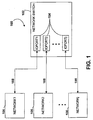
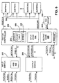
- the network switch 102 includes two or more input/output (I/O) ports, or "ioports" 104, each for coupling to and interfacing a network 106 through an appropriate cable segment 108.
- the ioports 104 are generally referred to as ioports indicative of bidirectional data flow, although each may be referred to as in input port when receiving data from a network 106 or an output port when transmitting data to a network 106.
- each network 106 is coupled to the switch 102 through a corresponding one of j ioports 104, individually labeled IOPORT1, IOPORT2, ..., IOPORTj.
- the network switch 102 may include any desirable number of ioports 104 ports for coupling up to an associated number of networks 106.
- j is an integer number ranging from 1 to 24 for a total of 24 ioports 104 and 24 networks 106.
- Each network 106 represents one or more data devices or data terminal equipment (DTE) that allows either input or output of data, or includes any type of network device for connecting together one or more data devices.
- NETWORK1 may include one or more computers, work stations, file servers, modems, printers, or any other device that receives or transmits data in a network, such as repeaters, switches, routers, hubs, concentrators, etc.
- each network 106 represents one or more data devices coupled through one or more segments, where the network switch 102 enables communication between any two or more data devices in any of the networks 106.
- the network switch 102 operates to receive information from data devices coupled to each of the ioports 104 and to route the information to one or more of the other ioports 104.
- the network switch 102 also filters the information by dropping or otherwise ignoring information received from a data device in one network 106 that is only intended for data devices in that same network.
- the data or information is in the form of packets, where the particular form of each packet depends upon the protocol supported by a given network 106.
- a packet is a predefined block of bytes, which generally consists of header, data, and trailer. The format of a given packet depends on the protocol that created the packet.
- the header usually includes a source address identifying a data device originating the packet and a destination address identifying the destination data device. The header may further indicate whether the packet is a multicast or broadcast packet intended for multiple destinations.
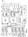
- the ioports 104 are essentially identical in structure and function, and are coupled to a switch matrix 200 for receiving and routing data packets.
- each ioport 104 provides received or "input" packets to an input switch 202 within the switch matrix 200 on respective data signals RXDATAn, where n is an integer from 1 to 26 corresponding to the particular data signal and port.
- RXDATAn data signals
- IOPORT1 provides received data packets on a signal RXDATA1 to one input of the input switch 202
- IOPORT2 provides data packets on a signal RXDATA2 to another input of the input switch 202, etc.
- each of the ioports 104 has an input for receiving output data packets from an output switch 204 within the switch matrix 200 on corresponding transmit data signals TXDATAn.
- IOPORT1 receives data packets on a signal TXDATA1 from one output of the output switch 204
- IOPORT2 receives data packets on a signal TXDATA2 from another output of the output switch 204, etc.
- Status and control signals for controlling communication and data transfer between each ioports 104 and the switch matrix 200 are described below.
- the input switch 202 has m output signals, collectively referred to as IBUFm, where m is an integer from 0 to 59 identifying individual signals IBUF0, IBLTF1, ... IBUF59.
- the IBUFm signals provide data to respective inputs of m memory packet buffers 206, individually referred to as BUFFERm or BUFFER0, BUFFER1, ... BUFFER59.
- BUFFERm m memory packet buffers 206
- there are sixty (60) packet buffers 206 where each has an output for providing data on a corresponding output signal OBLTFm to respective inputs of the output switch 204 within the switch matrix 200.
- a switch controller circuit 208 is shown coupled to the input switch 202, the output switch 204 and to each of the packet buffers 206 for controlling data flow.
- the switch controller 208 also asserts and detects other control signals to and from each of the ioports 104 as described further below.
- the switch controller 208 further includes or is otherwise coupled to a memory 210 for storing a packet table 604 ( Figure 6) and other information for tracking data flow.
- a packet processor 212 and a management processor 214 are both coupled to the switch matrix 200 in a similar manner as each of the ioports 104. As described further below, the packet processor 212 and the management processor 214 each appear as additional ports to the switch matrix 200. In particular, the packet processor 212 asserts data on a signal RXDATA25 to a corresponding input of the input switch 202, and receives data on a signal TXDATA25 from a corresponding output of the output switch 204. Likewise, the management processor 214 asserts data on a signal RXDATA26 to a corresponding input of the input switch 202 and receives data on a signal TXDATA26 from a corresponding output of the output switch 204.
- Hash logic 216 is coupled to each of the ioports 104, to the packet processor 212 and to the management processor 214 through a hash bus 218, which includes address, data and control signals.
- the hash logic 216 includes a hash memory 217, which is implemented using SRAM or the like for storage and retrieval of port number data, as further described below.
- the input switch 202 and the output switch 204 each include a plurality of "input" rows for connecting to "output" columns. In this manner, the input switch 202 connects any one of the ioports 104 to any one of the packet buffers 206 forming a serial data channel. Although the input switch 202 connects each of the ioports 104 to only one of the packet buffers 206 at a time, the input switch 202 allows a plurality of simultaneous serial connections between different ioports 104 and different packet buffers 206. Likewise, the output switch 204 connects each of the packet buffers 206 to any one of the ioports 104 and allows a plurality of simultaneous serial connections between different packet buffers 206 and different ioports 104.
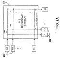
- FIG. 2A is a block diagram of an i by j crossbar switch 230 for implementing the input and output switches 202, 204 of Figure 2.
- the crossbar switch 230 includes i inputs In1, In2, ... Ini 232 and j outputs O1, O2, ... Oj 234, where i and j are integers for implementing any number of inputs 232 and outputs 234.
- i ranges from 1 to 26 and j ranges from 0 to 59.
- i ranges from 0 to 59 and j ranges from 1 to 26.
- the crossbar switch 230 includes a plurality of crosspoint connections 236 for connecting any input 232 to any output 234.
- the crossbar switch 230 enables simultaneous crosspoint connections between different inputs 232 and different outputs 234, although any particular input 232 is connected to only one output 234 at a time.
- the input and output switches 202, 204 may be implemented using other switching fabrics, such as Banyan fabric or the like using blocking or non-blocking formats.
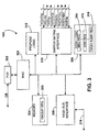
- a media access control (MAC) device 300 is the primary component for performing MAC functions.
- the MAC device 300 is protocol specific and operates at the MAC sub-layer, which is the lower sub-layer of the data-link layer of the OSI Reference Model. Examples include the TI Token Ring Eagle, TMS380C25, the AT&T (RTM)VG node interface chip, 2MD01, a custom designed MAC layer device with optimized interface, etc.
- a physical interface (PHY) 302 is coupled to the MAC device 300, where the PHY 302 is a protocol specific physical layer device for interfacing with the physical cable of the segment 108.
- PHY-type devices include the TI Token Ring Interface Chip, TMS38054, or the AT&T (RTM) 100VG transceiver, ATT2XO1, etc.
- the appropriate connector is also provided, such as, for example, an RJ-45 jack for interfacing a compatible RJ-45 plug for coupling to twisted-wire pairs. Twisted-wire pairs may be used for a variety of protocols, including various Ethernet standards such as 10Base-T, 100Base-TX, etc.
- a memory 304 is coupled to the MAC device 300 for temporarily storing one or 30 more data packets, or portions thereof, while a routing decision is made for those packets.
- the memory 304 also stores various other data and parameters as desired, and includes optional registers and buffers for particular implementations.
- the memory 304 includes an optional n-bit or 24-bit GROUP register 305 if the ioports 104 support input port packet replication.
- Each of the bits of the GROUP register 305 corresponds to one of the other ioports 104, where each bit is set for corresponding ioports 104 belonging to the same group. If the group function is implemented, then packets received are only relayed to one or more other members of the same group, and are otherwise dropped.
- a unicast packet for example, is dropped if its destination address is to an ioport 104 not within the same group as the input port. Multicast and broadcast packets are sent to one or more other ioports 104 belonging to the same group. If the GROUP register 305 is not included or if all of its bits are set or logic one, then the ioport 104 handles packets as further described below.
- Routing decisions are primarily performed in hash logic 306, which retrieves the source and destination addresses from each packet for determining to which of the other ioports 104, if any, that the packet should be sent.
- the hash logic 306 performs a hashing procedure for reducing the bit-size of each address to a smaller value, and for providing the hashed result through a hash bus interface 308 and the hash bus 218 to the hash memory 217.
- the hash memory 217 returns a port number or value identifying the destination port, if any or one of the processors 212, 214.
- the hash memory 217 returns the port number of the packet processor 212 for handling exceptional cases. As shown in Figure 2, the port number of the packet processor 212 is 25.
- a switch matrix interface 310 is provided for interfacing the ioport 104 with the switch matrix 200 through the RXDATAn and TXDATAn signals, as well as other control signals RXPENDn, RXENn, RXCLKn, TXPENDn, TXENn and TXCLKn, described below.
- Prepend logic 312 is coupled to the packet buffer 304 for prepending bytes of data to each of the input packets as further described below. Although each of the functional logic and memory blocks are shown separated, each of the ioports 104 is implemented and grouped in any suitable fashion, such as several chips, a single, integrated chip or an application specific integrated circuit (ASIC), etc.
- the hash logic 306 includes a MAC address register 314 for temporarily storing MAC addresses within packets received from a corresponding network 106.
- the MAC register 314 includes at least 48 bits ADD[47:0] for storing a MAC address.
- An address enable (AEN) register 316 is also provided and coupled to the MAC register 314, and also includes 48 bits AEN[47:0], each corresponding to a bit of the MAC register 314.
- the AEN register 316 stores a programmable enable pattern for selecting bits of the MAC address in the MAC register 314 for providing a hash address stored in a HASH register 318.
- the enable pattern is modified to optimize hash addresses in the event the default enable pattern results in a significant amount of hash address collisions. Any or pattern of bits may be selected, and the selected bits are consecutive or non-consecutive bits as determined by the packet processor 212.
- the number of selected bits equals the number of address bits for the hash memory 217, which in the embodiment shown is 15 bits for addressing 32K different addresses.
- the packet processor 212 generally performs five functions, including packet exception handling, learning bridge, spanning tree algorithm, MAC address map maintenance and hashing optimization, and system overhead.
- the packet processor 212 includes a switch matrix interface 400 for interfacing with the switch matrix 200 for sending and receiving packets through data signals RXDATA25 and TXDATA25, respectively, while using control signals RXPEND25, RXEN25, RXCLK25, TXPEND25, TXEN25 and TXCLK25, where the data and control signals for receive and transmit are collectively shown as signals RX25 and TX25, respectively.
- the packet processor 212 includes a processor 402 coupled to the switch matrix interface 400 for performing the functions listed above.
- a memory 404 is coupled to the processor 402 and the switch matrix interface 400 for storing startup and run-time routines and also for storing and retrieving parameters and data.
- the memory 404 includes read-only memory (ROM) 408 for storing startup routines to initialize the processor 402 and run-time routines performed by the processor 402.
- the memory 404 also includes DRAM 410 for storing parameters and data during run-time, and also an DRAM for storing a MAC address map 412 of all MAC addresses received at the ioports 104.
- the packet processor 212 also includes a hash bus interface 414 coupled to the switch processor 402 and the memory 404 for interfacing with the hash logic 216 and the hash memory 217 through the hash bus 218.
- the packet processor 212 asserts a write enable signal HASHWE* to update the hash memory 217 with new addresses when received by any of the ioports 104. Only the packet processor 212 asserts the HASHWE* signal for writing to the hash memory 217, so that the ioports 104 and the management processor 214 only have read access.
- a signal name followed by an asterisk (*) is considered negative logic, which is considered asserted when low, or at logic zero, and negated when high, or at logic one.
- the packet processor 212 asserts an output enable signal HASHOE* to enable the hash memory 217 to assert port numbers and other data on an 8-bit hash data bus HD[7:0].
- the ioports 104, the packet processor 212 and the management processor 212 assert hash addresses to the hash memory 217 on a 16-bit hash address bus HA[15:0].
- the hash bus interface 414 asserts an arbitration signal ARB25 for arbitrating for the hash bus 218, and an acknowledge signal ACK25 is asserted to grant control of the hash bus 218 to the packet processor 212. Hash bus arbitration is further described below.
- the packet processor 212 assesses the internal registers of the ioports 104 by driving the HA[15] bit of the hash address bus HA[15:0] high and setting the HA[14:10] bits equal to the binary physical port number. For example, the packet processor 212 can query the GROUP register 305, the AEN register 316, the HASH register 318, or any other register within an ioport 104.
- each ioport 104 compares the HA[14:10] bits with its own port number to determine if the hash bus cycle is directed towards that port.
- the HA[9:0] signals allow decoding of specific registers within each of the ioports 104.
- Each of the ioports 104 receives packets from corresponding networks 106 and retrieves the corresponding source and destination addresses within the packets.
- the source and destination addresses are typically 48-bit MAC addresses, which, according to industry standards, are guaranteed to be unique.
- a 15-bit address includes over 32,000 (32K) unique combinations, and thus is sufficient for distinguishing between over 32K total devices coupled through the ioports 104.
- the lower bits of the MAC address are incremented for each data device, so that the lower 15 bits of the address provides an initial or default hash address.
- the lower 15 bits do not guarantee a unique hash address and can result in an address collision, where the same hash address is generated from two different MAC addresses. If such collision results, then the ioport 104 routes the packet to the packet processor 212 through the switch matrix 200, as further described below.
- the packet processor 212 receives a packet from the switch matrix 200, determines the appropriate action for that packet, and then re-submits that packet to the switch matrix 200 for routing to one of the ioports 104.
- Packet exception handling includes identification of new MAC addresses and replicating packets to multiple ioports 104 for multiple destinations.
- the packet processor 212 updates the hash memory 217 with new addresses when received by any of the ioports 104.
- the learning bridge and spanning tree functions typically conform to the IEEE 802.1 specification for formulating an address to port map structure and identification of which of the ioports 104 are supported by the network switch 102. This information is stored in the MAC address MAP 412.
- Each of the ioports 104 perform minimal default hashing functions, which may result in the same hashed address for two different hash addresses.
- the packet processor 212 uses optimization techniques to identify and correct address collisions.
- the MAC address map 412 is a linked list structure including each MAC address received and the corresponding port number associated with that MAC address. For each MAC address, the MAC address map 412 also includes a list of associated MAC addresses, if any, and corresponding port numbers. Each packet indicates whether it is a unicast, multicast, or a broadcast packet.
- a unicast packet includes one source MAC address and one destination MAC address.
- a multicast packet also includes a source MAC address, but is associated with a group of individual MAC addresses of other data devices.
- a broadcast packet is a packet associated with one or more "virtual" segments, such as one or more segments 108.
- the packet processor 212 initializes the MAC address map 412 and the hash memory 217 upon power up, and then updates the MAC address map 412 and the hash memory 217 for each new packet.
- the packet processor 212 eventually updates the hash memory 217 to handle most transfers of unicast packets without intervention by the packet processor 212.
- the packet processor 212 also eventually updates the MAC address map 412 with all of the MAC addresses and ioports 104 associated with each multicast and broadcast packet.
- the packet processor 212 uses the address map to replicate each multicast and broadcast packet to the appropriate output ports.
- the packet processor 212 receives all packets containing new MAC addresses, and updates the MAC address map 412 and the hash memory 217.
- a new source MAC address is copied into the MAC address map 412 along with its corresponding port number.
- the port number is also written into the hash memory 217 at a hashed address location if there is no address collision between hashed addresses.
- the packet processor 212 writes its own port number of 25 into the hash memory 217, so that the next packet with the same hashed address is routed to the packet processor 212. If the packet is a unicast packet and its destination MAC address is unknown, then the packet processor 212 replicates the packet to all of the other ioports 104 other than the input port.
- the unicast packet is initially treated as a broadcast packet. For example, if a unicast packet with an unknown destination MAC address is received at IOPORT1, then the packet processor 212 replicates the packet to IOPORT2, replicates the packet to IOPORT3, replicates the packet to IOPORT4, etc., until the packet is repeated to all other IOPORTS 2-24. Eventually, the destination data device receives a copy of the replicated packet and responds with its own source MAC address. Since the source address from the destination data device is "new" in that the hash memory 217 has not yet been updated with the corresponding port number, the packet is routed to the packet processor 212. The packet processor 212 updates the hash memory 217 with the port number.
- any unicast packets sent from known source MAC addresses to that same destination data device are routed directly without intervention of the packet processor 212.
- Each ioport 104 detects an address collision by querying the hash memory 217 for the port number of an input packet's source MAC address and then comparing the port number received from the hash memory 217 with its own port number. If the port numbers are different, then an address collision has occurred and the input port routes the packet to the packet processor 212. In the embodiment shown, each ioport 104 routes all multicast and broadcast packets to the packet processor 212. Alternatively, the ioports 104 are configured to handle their own multicast and broadcast packets to reduce the processing load of the packet processor 212.
- FIG. 5 a more detailed schematic diagram is shown of the interface between the hash logic 216, the ioports 104 and the processors 212, 214 through the hash bus 218.
- Each of the ioports 104 and the processors 212, 214 assert a corresponding arbitration signal ARBn on the hash bus 218 to request ownership of the hash bus 218, where, as before, n is an integer between 1 and 26 identifying the port number or processor.
- An arbiter 500 within the hash logic 216 receives the ARBn signal and asserts a corresponding acknowledge signal ACKn to grant control of the hash bus 218.
- IOPORT1 asserts a signal ARB1 to request control, and the arbiter 500 respondingly asserts a signal ACK1 to grant control of the hash bus 218 to IOPORT1.
- the hash address bus is shown as HA and the hash data bus is shown as HD.
- a ioport 104 receives a packet and arbitrates for the hash bus 218 by asserting its corresponding ARBn signal. In response to its corresponding ACKn signal being asserted and while the ioport 104 owns the hash bus 218, it asserts a hash address on the HA[14:0] signals to the hash memory 217 for both the source MAC address and the destination MAC address in the packet.
- the frame type is either Ethernet or Token Ring, where it is understood that many other types of protocols may be included or substituted as desired.
- the Ethernet protocol includes a variety of data rates and speeds. Any particular data rate may be used at any particular ioport 104. In fact, hybrid operation is supported where different ioports 104 may operate at different data rates.
- the input port compares the OPNUM value for each address with its own port number. If the OPNUM of the destination address is equal to the port number of the input port, then the packet is dropped and ignored. If the OPNUM for the hashed source address equals the port number of the input ioport 104, then the source address has been previously established within the hash memory 217 by the packet processor 212, and no hash address collisions occurred. It is noted, however, that a hash address collision may occur between two data devices in the same network 106 coupled to the same input ioport 104. Although this may result in incomplete data of the MAC address map 214 within the packet processor 212, it is not required to distinguish between two different devices coupled to the same input port since packet routing is the same.
- BLOCK 1
- the ioport 104 drops the packet since this indicates that the network switch 100 does not service that ioport 104 according to the spanning tree algorithm. If spanning tree is not implemented, then BLOCK is set to zero.
- the TRFrame value indicates the destination port requires either Ethernet or Token Ring packet format. If the format received is not the same as the format required at the destination port, the input ioport 104 routes the packet to the management processor 214, if present, or otherwise drops the packet.
- the management processor 214 converts packet formats as necessary.
- the network switch 100 uses the prepended information to further process and route the packet to the desired output port or processor.
- the input switch 202 includes a receive data arbiter 602, which receives an RXPENDn signal from each of the ioports 104 indicating that the port has a pending packet to send to the switch matrix 200.
- IOPORT1 asserts a signal RXPEND1 to indicate it has a pending input packet
- IOPORT2 asserts a signal RXPEND2 to indicate it has a pending input packet, etc.
- Each of the ioports 104 keeps its respective RXPENDn signal asserted until after the packet is sent.
- the arbiter 602 scans all of the RXPENDn signals and asserts a corresponding receive enable signal RXENn to the requesting ioport 104 asserting its RXPENDn signal, or IOPORTn, to initiate transfer of the packet.
- the data from each of the ioports 104 is provided to the input switch 202 on a corresponding data signal RXDATAn at a rate identified by a corresponding receive clock signal RXCLKn.
- IOPORT10 in response to a signal RXEN10 being asserted by the input switch 202, IOPORT10 asserts an input packet on a signal RXDATA10, one bit at a time, and accordingly toggles a clock signal RXCLK10 with each bit. This establishes a separate receive data channel between each of the ioports 104 and the input switch 202.
- the switch controller 208 receives a master clock signal CLK from a clock circuit 603 for synchronizing data flow and transfers. Although not explicitly shown, the CLK signal is used by circuitry and logic described herein for purposes of synchronization
- the switch controller 208 includes input logic 606 for controlling the transfer of input packets from the ioports 104 to the packet buffers 206.
- the input logic 606 searches a BFREE register 605 in the memory 210 for the buffer number (m) of the next free packet buffer 206, or BUFFERm.
- the input logic 606 then asserts the equivalent binary buffer number on six buffer number signals SBUF[5:0] and asserts a buffer command signal SBUFCMD to prepare the next free packet buffer 206 to receive an input packet.
- each of the packet buffers 206 detects the SBUFCMD signal asserted and latches the binary number (m) asserted on the SBUF[5:0] signals. Each of the packet buffers 206 then compares the latched number (m) with its own physical number, and the indicated packet buffer 206 then monitors the duration of the SBUFCMD signal to determine the appropriate action In particular, the SBUFCMD signal is asserted for two CLK cycles to command the indicated packet buffer to free itself after transmitting a packet for output. The SBUFCMD signal is asserted for three CLK cycles to command the indicated packet buffer to begin transmitting a packet for output.
- the SBUFCMD signal is asserted for four CLK cycles to command the indicated packet buffer to prepare for an input packet from the input switch 202.
- the input logic 606 asserts the SBUFCMD for four CLK cycles to command the next free packet buffer BUFFERm to receive the next input packet.
- the input logic 606 also asserts the binary equivalent of the number (m) of the next free packet buffer 206 on present input buffer signals PIB[5:0] to the input switch 202.
- the input switch 202 establishes a crosspoint connection between the corresponding RXDATAn signal and the IBUFm signal of the corresponding free BUFFERm identified by the number (m) asserted on the PIB[5:0] signals.
- the input switch 202 then asserts the RXENn signal to indicate to the IOPORTn asserting its RXPENDn signal to send its packet, and in response to the assertion of the RXENn signal, the IOPORTn sends the packet.
- the input switch 202 detects the leading edge of the packet, which is the PREPEND[15] lead bit, and then latches the next PREPEND[14:10] bits defining the prepended output port number OPNUM from the packet stream.
- the input switch 202 toggles a signal PKTENTRY to the switch controller 208 to transmit the OPNUM.
- the switch controller 208 corresponds the PIB[5:0] number of the buffer where the packet is to be stored with the output port number OPNUM, which indicates the ioport 104 where the packet is to be sent.
- the input switch 202 also latches the PREPEND[9:8] bits defining the priority level of the input packet, and correspondingly toggles the PKTENTRY signal.
- the switch controller 208 further includes a 6-bit packet buffer capacity SWBCAP counter 607, which stores a binary number asserted on SWBCAP[5:0] signals representing the number of the packet buffers 206 containing data packets.
- the input logic 606 increments the SWBCAP counter 607 with each new input packet.
- IOPORTn After IOPORTn has finished sending the packet, it negates its RXPENDn signal.
- the input switch 202 respondingly negates the RXENn signal, and then performs a crosspoint clear process by clearing the crosspoint connection between the RXDATAn signal and the IBUFm signal. In this manner, the input switch 202 need only make and break the crosspoint connection, and does not need to know or otherwise measure the length of the packet.
- the memory 210 is implemented as random access memory (RAM), such as static RAM (SRAM) or dynamic RAM (DRAM), or any other type of suitable memory device for storage and retrieval of data during operation.
- RAM random access memory
- SRAM static RAM
- DRAM dynamic RAM
- the memory 210 is 8 kilobytes (Kbytes) and is organized into 128 blocks, where each block includes 64 bytes.
- the blocks 127 - 105 are not used, and the remaining blocks are allocated to form a cross reference packet table 604 between the packet buffers 206 and the ioports 104 according to the following Table IIIA: TABLE IIIA: ORGANIZATION OF PACKET TABLE 604 BLOCK NUMBER PORT NUMBER PRIORITY LEVEL 104 26 3 103 26 2 102 26 1 101 26 0 100 25 3 99 25 2 ... ... ...
- BFREE 605 N/A where "block” identifies the data location within the memory 210, "port” identifies the port number of the output port, and priority indicates the relative priority of information stored therein.
- the last BLOCK 0 is used to store the BFREE register 605 indicating which of the packet buffers 206 are free or contain data packets.
- blocks 127 - 27 are not used, and the remaining blocks are allocated to form a cross reference packet table 604 between the packet buffers 206 and the ioports 104 according to the following Table IIIB: TABLE IIIB: ALTERNATIVE ORGANIZATION OF PACKET TABLE 604 BLOCK NUMBER PORT NUMBER 26 26 25 25 24 24 23 23 22 22 21 21 ... ...
- Each of the packet buffers 206 includes enough memory to contain one packet of data having a maximum size, since packet size varies. Ethernet packet sizes may be as large as 1,500 bytes, whereas Token Ring packet sizes may be as large as 17,960 bytes or more. Token Ring networks generally provide a network parameter to set the maximum packet size. In the embodiment shown, however, each of the packet buffers 206 include 4 Kbytes of memory, thereby limiting packet size to a maximum of 4 Kbytes.
- the circular buffer within each of the blocks includes 60 bytes, each byte for storing a buffer number SBUFNUM, ranging from 0 to m, to point to one of the packet buffers 206, if necessary, containing data packets for the associated output port.
- each circular buffer forms a first-in, first-out (FIFO) pointer list for a particular IOPORTn to ensure the data packets are output to the port in received order.
- the write pointer WPTR points to the last byte location of the pointer list, and is modified or "incremented" to point to any further packet buffers 206 containing new input packets.
- the switch controller 208 includes output logic 608 for controlling the transfer of pending output packets from the packet buffers 206 to the ioports 104.
- the output logic 608 asserts a signal TXPENDn to the corresponding IOPORTn when a pending packet is stored in one of the packet buffers 206 for that IOPORTn.
- Each of the ioports 104 asserts a corresponding transmit enable signal TXENn in response to its TXPENDn signal being asserted, thereby indicating that it is ready to receive the pending packet.
- TXPENDn and 26 TXENn signals there are 26 TXPENDn and 26 TXENn signals, one each for each of the ioports 104 and one each for the processors 212 and 214.
- the output logic 608 In response to the TXENn signal being asserted, the output logic 608 identifies the BUFFERm holding the next packet for the IOPORTn asserting the TXENn signal, negates the TXPENDn signal, and asserts the appropriate binary numbers on output crosspoint signals OCROSS[5:0]. Also, the output logic 608 asserts an output crossbar command signal OCROSSCMD to make the appropriate output crosspoint connection between BUFFERm and IOPORTn through corresponding signals OBUFm and TXDATAn.
- a binary number indicating the packet buffer 206 or BUFFERm holding the packet for output is asserted on the OCROSS[5:0] signals to the output switch 204, and the OCROSSCMD is asserted.
- the output switch 204 detects the assertion of the OCROSSCMD signal and latches the buffer number (m) from the OCROSS[5:0] signals.
- a binary number indicating the output port number (n) of IOPORTn is asserted on the OCROSS[5:0] signals, which signals are latched by the output switch 204.
- the output switch 204 samples the OCROSSCMD signal to determine whether a make or break command is being sent. If the OCROSSCMD signal is asserted for only two CLK cycles, then a break process occurs where the output switch 204 respondingly breaks the connection between OBUFm and TXDATAn. If the OCROSSCMD signal is asserted for three CLK cycles, then a connection process occurs where the output switch 204 respondingly establishes a crosspoint connection between OBUFm and TXDATAn.
- the output logic 608 then asserts the buffer number (m) on the SBUF[5:0] signals and asserts the SBUFCMD for three CLK cycles to command the identified BUFFERm to initiate data transfer. It is noted that the particular timing between the SBUF and OCROSS signals may be implemented in any desired manner to establish the connection and initiate the output data packet transfer as long as the connection is made before actual data transfer begins.
- the output logic 608 also decrements the SWBCAP value stored in the SWBCAP counter 607 for each packet output to an ioport 104.
- the output switch 204 transfers output data packet from the BUFFERm on the OBUFm signal to the TXDATAn signal of the corresponding IOPORTn.
- the IOPORTn toggles a corresponding transmit clock signal TXCLKn to the output switch 204 to enable IOPORTn to control the rate of transfer of the output packet.
- IOPORTn then negates its TXENn signal when the transfer of the output data packet is completed.
- the output logic 608 detects the negation of the TXENn signal, and then asserts the packet buffer and output port numbers on the OCROSS[5:0] signals and asserts the OCROSSCMD signal for two CLK cycles to command the output switch 204 to break the crosspoint connection, as described previously.
- the output logic 608 then asserts the packet buffer number (m) on the SBUF[5:0] signals to identify the BUFFERm, and then asserts the SBUFCMD signal for two CLK cycles to command the indicated BUFFERm to free itself for another packet of data.
- the general process of receiving and storing an entire packet before retransmitting the packet for output is referred to as store-and-forward operation. Cut-through operation is also supported, where after a connection is established between an IOPORTn and a BUFFERm for receiving an input packet, that BUFFERm begins transmitting through the output switch 204 to another IOPORT before receipt of the end of packet if instructed to do so by the switch controller 208.
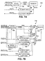
- FIGs 7A and 7B are schematic diagrams showing alternative implementations of the packet buffers 206.
- a packet buffer 700 is shown for supporting one packet per BUFFERm.
- the IBUFm, SBUFCMD and SBLTF[5:0] signals are provided to the inputs of a state machine 702, which detects assertions of the SBLTFCMD, latches the SBUF[5:0] bits and then monitors the SBUFCMD to determine the appropriate action.
- the state machine 702 asserts an address to the address input of a memory 704 for addressing individual bits of the packet, and asserts a read/write signal R/W indicating either input to or output from the memory 704.
- the data bits asserted on the IBUFm signal are also provided to an input shift register 706, which provides data bits one at a time to the data input of the memory 704.
- the memory 704 asserts output data bits to the input of an output shift register 708, which asserts the data bits on the OBUFm signal.
- a packet buffer 710 is shown for supporting multiple or k packets per BUFFERm, where k is any desired integer ranging from depending upon buffer size and available size of a memory 716. For example, 32K by 8 SRAMs are commonly available, and if packet length is limited to a maximum size of 4Kbytes, then 8 packets per BUFFERm is supported as long as the data rate of the IBUFm and OBUFm signals is less than the access time of the memory 716. For 8 packets per BUFFERm, k ranges from 1 to 8 to identify individual packet inputs and outputs.
- the SBUF[5:0], SBUFCMD and a respective one of k data input signals IBUF(m) to IBUF(m+k) are provided to respective inputs of k state machines 702.
- the first state machine 702 receives an IBUF(m) signal
- the second receives an IBUF (m+1) signal
- ... the last receives an IBUF (m+k) signal.
- the k outputs of the k state machines 702 are provided to a k-input multiplexer (mux) 712, which receives the integer k as a select input for asserting a selected memory address at its output to the memory 716.
- Each of the state machines 702 also asserts a corresponding R/W signal to k inputs of another k-input mux 718 receiving k as its select input, where the selected R/W signal is provided to the R/W input of the memory 716.
- the respective IBLTF(m) to IBUF(m+k) input signals are also provided to the inputs of k input latch and shift registers 720, which assert outputs to respective inputs of a k-input and k-output bidirectional mux 714.
- the mux 714 receives k as a select input and the R/W signal from the mux 718 indicating direction of data flow.
- the mux 714 has k outputs provided to respective inputs of k output latch and shift registers 722, which assert outputs on k respective output signals OBUFm to OBUF(m+k).
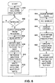
- a flowchart diagram is shown illustrating operation of the input logic 606 for controlling input packet flow.
- the input logic 606 may be implemented in any suitable manner as known to those skilled in the art, such as a state machine triggered on the PKTENTRY signal.
- a first step 800 the input logic performs initialization, including preparing the first BUFFER0 to receive data.
- the input logic 606 then periodically monitors the PKTENTRY signal in next step 802, which is asserted when a new packet is being provided from the input switch 202. Operation remains in step 802 until the PKTENTRY signal is asserted.
- step 804 When the PKTENTRY signal is asserted, operation proceeds to next step 804, where the OPNUM asserted on the PKTENTRY signal is latched or otherwise captured. Also, priority information is captured in step 804 if supported. Operation then proceeds to step 806, where the WPTR write pointer is retrieved from the block in the packet table 604 of the memory 210 corresponding to the OPNUM. If priority is supported, then the WPTR pointer of the indicated priority is retrieved. The WPTR value is then modified to point to the next available location in the circular buffer, and the modified WPTR is stored into the block in a next step 808.
- next step 810 the SBUFNUM buffer number (m) indicating the next free packet buffer 206 BUFFERm is retrieved from the PIB[5:0] signals. SBUFNUM is then written into the first location pointed to by WPTR of the circular buffer of the corresponding block in next step 812. Then, operation proceeds to next step 814, where the BFREE flag associated with the freed buffer BUFFERm is cleared indicating that BUFFERm contains data.
- the SWBCAP counter 607 is incremented in next step 816.
- next step 818 the TXPENDn signal corresponding to OPNUM is asserted to inform the IOPORTn that data is pending for output for that port.
- the input logic 606 then scans the BFREE register 605 to find the next free packet buffer 206 in next step 820. Then, the PIB[5:0] bits are updated with the number of the next free packet buffer 206 for the next packet of data in next step 822. Finally, the next free buffer number is asserted on the SBUF[5:0] signals and the SBUFCMD signal is asserted for four CLK signals to command the next free packet buffer 206 indicated by SBUF[5:0] to prepare to receive the next input packet. Operation then returns to step 802 to monitor the PKTENTRY signal for the next packet.
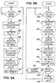
- each of the TXENn signals corresponding to TXPENDn signals being asserted are periodically sampled to determine if a rising edge occurs. If not, operation loops back to step 900.
- An alternative to such periodic polling is an interrupt generated in response to a rising edge of the TXENn signals.
- next step 904 If any of the TXENn signals are asserted high by an IOPORTn, operation proceeds to next step 904, where the corresponding TXPENDn signal is negated. Operation proceeds to next step 906, where the RPTR read pointer is retrieved from the block in the packet buffer table 604 corresponding to the IOPORTn asserting the TXENn signal.
- next step 908 is the buffer number of the BUFFERm holding a pending packet for output to the port asserting the TXENn signal.
- next step 910 the OCROSS[5:0] signals are asserted with and the buffer number (m) of the packet buffer 206 holding the pending packet, and the OCROSSCMD signal is asserted. Then, the OCROSS[5:0] signals are asserted with the output port number (n) of IOPORTn, the destination port.
- the output switch 204 respondingly sets a crosspoint connection to connect the corresponding OBUFm and TXDATAn signals between the indicated packet buffer 206 and the output IOPORTn.
- next step 912 the SBUF[5:0] bits are asserted by the switch controller 208 to identify the BUFFERm, and the SBUFCMD signal is asserted for 3 CLK cycles to command the indicated packet buffer 206 to begin transmitting data.
- operation proceeds to next step 913 to decrement the SWBCAP counter 607, and then operation loops back to step 900 to determine the next rising edge of any of the TXENn signals.
- the switch controller 208 is immediately free to coordinate the next crosspoint connection.
- step 9B if any of the TXENn signals is high and then negated by an IOPORTn indicating data transfer has completed, operation proceeds from step 902 to step 914, where the read pointer RPTR is retrieved from the block corresponding to the IOPORTn.
- step 916 the SBUFNUM of the BUFFERm pointed to by RPTR is retrieved.
- the switch controller 208 then asserts the OCROSS[5:0] bits and the OCROSSCMD signal to clear the crosspoint connection in the output switch 204 in next step 918.
- step 920 the switch controller 208 asserts the SBUF[5:0] bits and the SBUFCMD signal to command the indicated BUFFERm to free itself for a new input packet.
- step 922 the WPTR write pointer is retrieved to determine pointer action.
- the RPTR read pointer is modified in next step 924 in the corresponding block of the packet table 604 to point to the next location in the circular buffer.
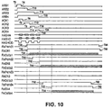
- FIG. 10 a timing diagram is shown illustrating data transfer timing of input packets from the ioports 104 to the input switch 202.
- the ARB1, ARB2, ARB3 and ARB4 signals are asserted by IOPORT1, IOPORT2, IOPORT3 and IOPORT4, respectively, indicating packets have been received by these input ioports 104.
- the ioports 104 continue to assert their corresponding ARBn signals until after they have gained control of the hash bus 218 and retrieve data from the hash memory 217.
- the Arbiter 500 asserts the ACK1 signal at subsequent time T2 granting control of the hash bus 218 to IOPORT1.
- IOPORT1 asserts a hashed address to the hash memory 217, which responds with hash data including an output port number.
- IOPORT1 receives and latches the hash data from the hash bus 218, and negates the ARB 1 signal at approximately time T4.
- the arbiter 500 respondingly negates the ACK1 signal at approximately time T6, and then asserts the ACK2 signal at approximately time T8 to grant control of the hash bus 218 to IOPORT2.
- IOPORT2 operates in a similar manner and retrieves hash data from the hash memory 217, and then negates the ARB2 signal at approximately time T10.
- the arbiter 500 respondingly negates the ACK2 signal at approximately time T12, and subsequently asserts the ACK3 signal at approximately time T14.
- IOPORT3 retrieves its hash data, negates the ARB3 signal at approximately time T16, and the arbiter 500 negates the ACK3 signal at approximately time T18 and grants control to IOPORT4 by asserting the ACK4 signal at time T20.
- IOPORT4 operates in a similar manner as IOPORTS 1-3 and completes at a subsequent time T22.
- IOPORT1 After IOPORT1 negates the ARB1 signal at time T4, it prepends information to the front of its packet and asserts the RXPFND1 signal at approximately time T30 to send data to the input switch 202. It is noted that time T30 is not necessarily subsequent to times T6, T8, T10, etc., and occurs as soon after time T4 that IOPORT1 is ready to send its packet.
- the input switch 202 subsequently asserts the RXEN1 signal at approximately time T32, and IOPORT1 sends data on the RXDATA1 signal to the input switch 202 beginning at approximately time T34. Meanwhile, after IOPORT2 negates the ARB2 signal and is ready to transmit its packet, IOPORT2 asserts the RXPEND2 signal at approximately time T40.
- the input switch 202 asserts the RXEN2 signal.
- IOPORT2 begins transmitting its packet to the input switch 202 on the RXDATA2 signal.
- IOPORT3 drops its packet and thus does not assert the RXPEND3 signal.
- IOPORT4 asserts the RXPEND4 signal to send its packet.
- the input switch 202 asserts the RXENn signal at subsequent time T52, and IOPORT4 begins sending its packet at approximately time T54 on the RXDATA4 signal.
- the packet being sent by IOPORT4 is a relatively short packet, and its transmission completes at about time T60.
- IOPORT4 then negates the RXPEND4 signal at approximately time T60, and the input switch 202 respondingly negates the RXEN4 signal at approximately time T62 indicating transfer is completed.
- IOPORTS 1 and 2 finish sending their respective packets and negate their corresponding RXPENDn signals, and the input switch 202 respondingly negates the corresponding RXENn signals.
- a timing diagram is shown illustrating data packet transfer timing between the output switch 204 and the ioports 104.
- the TXPEND1, TXPEND2 and TXPEND3 signals are all asserted by the switch controller 208 indicating that packets are pending for these ports.
- the corresponding TXEN1, TXEN2 and TXEN3 signals are initially negated at time T70.
- the TXEN1, TXEN2 and TXEN3 signals are asserted by IOPORTS 1-3, respectively. Simultaneous assertion of these signals is arbitrary and shown for only purposes of explanation.
- the output switch 204 establishes a crosspoint connection for IOPORT1, and the switch controller 208 then negates the TXPEND1 signal at approximately time T74 indicating a packet is to be transferred to IOPORT1.
- the packet is transferred on the TXDATA1 signal from a packet buffer 206 beginning at time T76.
- the switch controller 208 negates the TXPEND2 signal at approximately time T78.
- a packet is sent through the output switch 204 on the TXDATA2 signal beginning at time T80.
- a crosspoint connection is made for IOPORT3, and the switch controller 208 negates the TXPEND3 signal at approximately time T82.
- the output switch 204 then transmits a packet on the TXDATA3 signal beginning at time T84.
- Each of the IOPORTS 1-3 continues asserting its corresponding TXENn signal until after the packet is completely transferred.
- IOPORT2 negates the TXEN2 signal at approximately time T86 after it detects the end of the packet on TXDATA2.
- the output logic 608 subsequently detects another packet for IOPORT2, and asserts the TXPEND2 signal again at time T88.
- a switching network provides a data path between each I/O port and a plurality of packet buffers, so that the packet buffers are centrally located and not associated with only particular input or output ports.
- the packet buffers are available on a first-come, first-served basis to all of the ports.
- the switching fabric includes control logic and memory for tracking the packets stored in the packet buffers for each output port.
- the I/O ports include logic for prepending the output or destination port for each packet, which prepended information is intercepted by the control logic for tracking purposes.
- a packet processor handles new addresses and also handles packets to be duplicated, such as multicast and broadcast packets.
- the packet processor is coupled to the switching network in a similar manner as the I/O ports, where multicast and broadcast packets and packets with new addresses are simply routed to the packet processor.
- the packet processor updates an address table and duplicates the packet to each of the appropriate output ports by prepending the information to the packets.
Description
- The present invention relates to the field of networking devices, and more particularly to a network switch for transferring packets if information.
- There are many different types of networks and network systems for sharing files and resources or for otherwise enabling communication between two or more computers. Networks may be categorized based on various features and functions, such as message capacity, range over which the nodes are distributed, node or computer types, node relationships, topology or logical and/or physical layout, architecture based on cable type and data packet format, access possibilities, etc. For example, the range of a network refers to the distance over which the nodes are distributed, such as local-area networks (LANs) within an office or floor of a building, wide-area networks (WANs) spanning across a college campus, or a city or a state, global-area networks (GANs) spanning across national boundaries, etc.
- The architecture of a network generally refers to the cabling or media and media access used as well as the packet structure of the data transmitted across the media. Various architectures are common, including Ethernet using coaxial, twisted pair or fiber-optic cables for operation at 10 megabits per second (Mbps) (e.g. 10Base-T, 10Base-F) or fast Ethernet operating at 100 Mbps (e.g. 10OBase-T, 10OBase-FX). ARCnet (Attached Resource Computer Network) is a relatively inexpensive network architecture using coaxial, twisted pair or fiber-optic cables for operation at 2.5 Mbps. Token Ring topologies use special IBM cable or fiber-optic cable for operation between 1-16 Mbps. Of course, many other types of networks are known and available.
- Each network generally includes two or more computers, often referred to as nodes or stations, which are coupled together through selected media and various other network devices for relaying, transmitting, repeating, translating, filtering, etc., the data between the nodes. The term "network device" generally refers to the computers and their network interface cards (NICs) as well as various other devices on the network, such as repeaters, bridges, switches, routers, brouters, to name a few examples.
- A network segment is a group of stations that share the same data-link layer using the same data-link layer protocol. The data-link layer is the next layer above the lowest layer of the Open Systems Interconnection (OSI) Reference Model, where the lowest layer is referred to as the physical layer. Ownership of the data-link layer is established in accordance with the protocol, but only one station owns the data-link layer at a time. A network operating according to a given communications protocol may be expanded by using one or more repeaters. A repeater is a hardware device that functions at the physical layer and is used to connect two or more stations of the same network. In particular, a repeater receives packets or data from a data device in one station and re-transmits the packets to another station. Network repeaters support a network segment, but allow a star-wired topology to appear as a single segment. One particular disadvantage of repeaters is that they generate a significant amount of extraneous data traffic, since every data packet is repeated to every other device even though a packet may only be intended for one data device.
- A bridge is a hardware device that passes packets from one network segment to another. Bridges also operate at the data-link layer of OSI Reference Model and allow several segments to appear as a single segment to higher level protocols or programs. A bridge serves both as a medium (the bridge part) and as a filter by dropping packets that need not be relayed to other segments. In particular, a bridge provides packet filtering functions that reduce the amount of unnecessary packet propagation on each network segment. For example, a two-port bridge allows connectivity between two separate network segments. If the packet source and destination are on the same network segment, propagation to another segment is avoided, thereby increasing availability of the segment to attached stations. A multi-port bridge extends the two-port bridge to support a greater number of segments.
- The networking industry generally uses the terms "bridge" and "switch" interchangeably, since, externally, they perform the same or very similar functions. For example, a switch is similar in function to a multi-port bridge. However, a distinction is made based upon whether a packet passes through a common data path between data ports, which is the case for a bridge, or whether the packet passes through independent, concurrent data paths, referred to as a switch fabric or simply "switches", which is the case for a switch. A bridge interfaces each port to a common processor bus and performs store and forward operations. In particular, a processor receives a packet from one port via a common bus, determines the destination node or station, and re-transmits the packet to the port associated with the destination node via the common bus. In contrast, a switch interfaces each port to a switch fabric, where each port has an independent data channel to the switch fabric.
- A switch often must replicate multicast or broadcast packets to several other ports, where such replication is typically performed in the switch fabric. In one approach, the switch fabric simultaneously connected an input port to several output ports. However, this architecture resulted in significant latency since the switch fabric had to wait until all of the output ports were available. In another approach, the switch fabric established a connection to each output port, one at a time, and then sent the packet to the connected output port. Such sequential operation added significant complexity to the switch fabric. Furthermore, multiple broadcast packets received at about the same time often caused bottlenecks and dropped packets.
- Switches have included buffers at the input or the output of the switch fabric, so that the buffers were associated with the input or output ports of the switch. Buffers have also been distributed in a Banyan structure switching matrix, but this required several layers of buffers distributed throughout the Banyan structure. Also, buffers within Banyan structures were associated with certain ports and thus are not available to all ports.
- EP-A-0658027 discloses a packet switching system in which an intermediate packet switch is connected between an upstream packet switch and a downstream packet switch. Input ports of the intermediate switch each include buffering for temporarily storing a single packet. A router transfers a data packet, received by an input port from the upstream switch, over a data bus to a shared memory and subsequently transfers the data packet from the shared memory over the data bus and an output port of the intermediate switch to the downstream switch.
- EP-A-0339809 discloses an asynchronous time division packet data network including a switching matrix having a plurality of input ports and plurality of output ports means is provided for routing each data packet from an input port to a defined output port.
- It is desired to provide a network switch with improved switching fabric with increased data throughput.
- US-A-5091905 discloses a network switch for transferring data packets, comprising: a plurality of network ports; a plurality of packet buffers; a switch matrix coupled to said plurality of network ports; and a switch controller coupled to said switch matrix.
- The present invention is characterised in that
- each network port comprises a network input and output port; said switch matrix is coupled between said network input/output ports and said packet buffers and is operable under control of said switch controller to provide an input data channel between any one of said plurality of network input/output ports and any one of said plurality of packet buffers, and is independently operable under control of said switch controller to provide an output data channel between any one of said plurality of packet buffers and any one of said plurality of network input/output ports.
- In this manner, all of the packet buffers are shared and accessible by any of the network ports through the switch matrix. In one embodiment, each of the packet buffers stores only one packet of data at a time, although the packet buffers may be expanded to store multiple data packets.
- The switch matrix may include programmable input channel connections for providing at least two simultaneous input data channels and at least two simultaneous output data channels at a time. More particularly, the switch matrix may include an input switch with inputs coupled to the network ports, outputs coupled to respective inputs of the packet buffers and a plurality of programmable crosspoints. Furthermore the switch matrix may include an output switch with inputs coupled to respective outputs of the packet buffers, outputs coupled to the network ports and a plurality of programmable crosspoints. The input switch thus provides a data path between any one of the network ports and any one of the packet buffers. The input switch may include a plurality of programmable data paths for establishing simultaneous data connections between each of the ports with different ones of the buffers. The output switch operates in a similar manner and enables a data path between any one of the packet buffers and any one of the ports. The output switch enables simultaneous data connections between each of the network ports with different ones of the packet buffers at a time.
- The switch controller may include input logic for controlling transfer of input data packets, where the input logic determines a free packet buffer and asserts a corresponding buffer number. Each network port indicates a received data packet and prepends an output port number to the received data packet, and the switch matrix receives the buffer number of the free packet buffer and establishes a data channel between the network port which received the data packet and the free packet buffer. The switch matrix indicates to the network port to send the data packet with the prepended output port number, and the switch matrix receives the data packet, retrieves the output port number and provides the output port number to the input logic.
- The switch controller may further include output logic for determining if any of the packet buffers has data for any one of the network ports, and if so, the output logic asserts a transmit pending signal. Each of the network ports receives a corresponding transmit pending signal and asserts a corresponding enable signal indicating it is available to receive a data packet. The output logic provides a port number to the switch matrix identifying one of the network ports and provides a buffer number identifying one of said plurality of packet buffers storing data for that network port, where the switch matrix establishes an output data channel between the network port and the packet buffer. The output logic preferably includes logic for commanding each of the packet buffers to transmit a data packet.
- The switch controller may further include memory for a packet table which stores buffer numbers corresponding to the packet buffers storing data for the network ports. In the embodiment described herein, the packet table is organized into blocks corresponding to each of the network ports, where each of the blocks includes a circular buffer implemented as a first-in, first-out (FIFO) circular buffer for storing the buffer numbers. The input logic generally builds the packet table while the output logic uses the table to determine the output ports of the data packets.
- The network switch may include a hash memory for storing a table of network port numbers corresponding to hash addresses of the network ports. Each of the network ports may include hash logic for converting a media access control (MAC) address from each data packet into a hash address. Each network port provides the hash address to the hash memory for retrieving a corresponding network port number. The network switch further includes a packet processor for sending data packets to and for receiving data packets from the switch matrix. In particular, the packet processor receives data packets with a new address and duplicates multicast and broadcast data packets.
- A network system may be provided comprising a plurality of external network segments, each including at least one data device for sending and receiving data packets, and the network switch for transferring data packets between the networks.
- According to a second aspect of the invention there is provided a method of transferring a data packet a by a network switch including a plurality of network ports coupled to one or more networks, a plurality of packet buffers and a switch matrix operable under control of a switch controller, characterised by:
- receiving a data packet at a first network input/output port of the network switch for sending to a second network input/output port of the network switch;
- identifying an available one of said packet buffers from all of the plurality of packet buffers;
- operating the switch controller and the switch matrix to:
- establish an input data channel in the switch matrix between the first network input/output port and the identified packet buffer; and
- send the data packet to the identified packet buffer on the input data channel for temporary storage;
- determining when the second network input/output port is ready to receive the pending data packet stored by the identified packet buffer; and
- operating the switch controller and the switch matrix to:
- establish an output data channel in the switch matrix between the identified packet buffer and the second network input/output port; and
- sending the pending data packet from the identified packet buffer to the second network input/output port on the output data channel.
- In this manner, a network switch according to the present invention provides an improved switch fabric by providing shared buffers available to each of the network ports.
- A better understanding of the present invention can be obtained when the following detailed description of the preferred embodiment is considered in conjunction with the following drawings, in which:
- Figure 1 is a simplified network diagram of a network system including a network switch according to the present invention;
- Figure 2 is a more detailed block diagram of the network switch of Figure 1;
- Figure 2A is a more detailed block diagram of one embodiment of the input and output switches of Figure 2;
- Figure 3 is a block diagram of one of the ports of the network switch of Figure 1;
- Figure 4 is a simplified block diagram of the packet processor of Figure 2;
- Figure 5 is a more detailed schematic diagram of the interface between the hash logic, the ports and the processors of Figure 2;
- Figure 6 is a more detailed block diagram of the interface and control signals between the input and output switches, the switch controller and each of the packet buffers of Figure 2;
- Figures 7A and 7B are schematic diagrams showing alternative implementations of the packet buffers of Figure 6.
- Figure 8 is a flowchart diagram illustrating operation of the input logic shown in Figure 6 for controlling input packet flow;
- Figure 9A and 9B are flowchart diagrams illustrating operation of the output logic shown in Figure 6 for controlling output packet flow;
- Figure 10 is a timing diagram illustrating data packet transfer timing of input packets from the ports to the input switch of Figure 2; and
- Figure 11 is a timing diagram illustrating data packet transfer timing between the 30 output switch and the ports of Figure 2.
- Referring now to Figure 1, a simplified network diagram is shown of a
network system 100 including anetwork switch 102 implemented according to the present invention. Thenetwork switch 102 includes two or more input/output (I/O) ports, or "ioports" 104, each for coupling to and interfacing anetwork 106 through anappropriate cable segment 108. Theioports 104 are generally referred to as ioports indicative of bidirectional data flow, although each may be referred to as in input port when receiving data from anetwork 106 or an output port when transmitting data to anetwork 106. As shown, there are "n"networks 106 individually labeled NETWORK1, NETWORK2, ... NETWORKj, where eachnetwork 106 is coupled to theswitch 102 through a corresponding one ofj ioports 104, individually labeled IOPORT1, IOPORT2, ..., IOPORTj. Thenetwork switch 102 may include any desirable number ofioports 104 ports for coupling up to an associated number ofnetworks 106. In the specific embodiment shown, j is an integer number ranging from 1 to 24 for a total of 24ioports 104 and 24networks 106. - Each
network 106 represents one or more data devices or data terminal equipment (DTE) that allows either input or output of data, or includes any type of network device for connecting together one or more data devices. For example, NETWORK1 may include one or more computers, work stations, file servers, modems, printers, or any other device that receives or transmits data in a network, such as repeaters, switches, routers, hubs, concentrators, etc. In general, eachnetwork 106 represents one or more data devices coupled through one or more segments, where thenetwork switch 102 enables communication between any two or more data devices in any of thenetworks 106. - The
network switch 102 operates to receive information from data devices coupled to each of theioports 104 and to route the information to one or more of theother ioports 104. Thenetwork switch 102 also filters the information by dropping or otherwise ignoring information received from a data device in onenetwork 106 that is only intended for data devices in that same network. The data or information is in the form of packets, where the particular form of each packet depends upon the protocol supported by a givennetwork 106. A packet is a predefined block of bytes, which generally consists of header, data, and trailer. The format of a given packet depends on the protocol that created the packet. The header usually includes a source address identifying a data device originating the packet and a destination address identifying the destination data device. The header may further indicate whether the packet is a multicast or broadcast packet intended for multiple destinations. - Referring now to Figure 2, a more detailed block diagram is shown of the
network switch 102. Theioports 104 are essentially identical in structure and function, and are coupled to aswitch matrix 200 for receiving and routing data packets. In particular, eachioport 104 provides received or "input" packets to aninput switch 202 within theswitch matrix 200 on respective data signals RXDATAn, where n is an integer from 1 to 26 corresponding to the particular data signal and port. For example, IOPORT1 provides received data packets on a signal RXDATA1 to one input of theinput switch 202, IOPORT2 provides data packets on a signal RXDATA2 to another input of theinput switch 202, etc. In a similar manner, each of theioports 104 has an input for receiving output data packets from anoutput switch 204 within theswitch matrix 200 on corresponding transmit data signals TXDATAn. For example, IOPORT1 receives data packets on a signal TXDATA1 from one output of theoutput switch 204, IOPORT2 receives data packets on a signal TXDATA2 from another output of theoutput switch 204, etc. Status and control signals for controlling communication and data transfer between each ioports 104 and theswitch matrix 200 are described below. - The
input switch 202 has m output signals, collectively referred to as IBUFm, where m is an integer from 0 to 59 identifying individual signals IBUF0, IBLTF1, ... IBUF59. The IBUFm signals provide data to respective inputs of m memory packet buffers 206, individually referred to as BUFFERm or BUFFER0, BUFFER1, ... BUFFER59. Thus, in the embodiment shown, there are sixty (60) packet buffers 206, where each has an output for providing data on a corresponding output signal OBLTFm to respective inputs of theoutput switch 204 within theswitch matrix 200. In this manner, data packets received through any one of theioports 104 is directed through theinput switch 202 and temporarily stored in one or more of the packet buffers 206, and the data packet is redirected through theoutput switch 204 to one of theioports 104 to one or more destination data devices within anetwork 106. Aswitch controller circuit 208 is shown coupled to theinput switch 202, theoutput switch 204 and to each of the packet buffers 206 for controlling data flow. Theswitch controller 208 also asserts and detects other control signals to and from each of theioports 104 as described further below. Theswitch controller 208 further includes or is otherwise coupled to amemory 210 for storing a packet table 604 (Figure 6) and other information for tracking data flow. - A
packet processor 212 and amanagement processor 214 are both coupled to theswitch matrix 200 in a similar manner as each of theioports 104. As described further below, thepacket processor 212 and themanagement processor 214 each appear as additional ports to theswitch matrix 200. In particular, thepacket processor 212 asserts data on a signal RXDATA25 to a corresponding input of theinput switch 202, and receives data on a signal TXDATA25 from a corresponding output of theoutput switch 204. Likewise, themanagement processor 214 asserts data on a signal RXDATA26 to a corresponding input of theinput switch 202 and receives data on a signal TXDATA26 from a corresponding output of theoutput switch 204. However, thepacket processor 212 and themanagement processor 214 are not directly connected to anyexternal segments 108.Hash logic 216 is coupled to each of theioports 104, to thepacket processor 212 and to themanagement processor 214 through ahash bus 218, which includes address, data and control signals. Thehash logic 216 includes ahash memory 217, which is implemented using SRAM or the like for storage and retrieval of port number data, as further described below. - The
input switch 202 and theoutput switch 204 each include a plurality of "input" rows for connecting to "output" columns. In this manner, theinput switch 202 connects any one of theioports 104 to any one of the packet buffers 206 forming a serial data channel. Although theinput switch 202 connects each of theioports 104 to only one of the packet buffers 206 at a time, theinput switch 202 allows a plurality of simultaneous serial connections betweendifferent ioports 104 and different packet buffers 206. Likewise, theoutput switch 204 connects each of the packet buffers 206 to any one of theioports 104 and allows a plurality of simultaneous serial connections betweendifferent packet buffers 206 anddifferent ioports 104. - The input switches 202 and 204 may be implemented in any desired manner for establishing connections between respective inputs and outputs. Figure 2A is a block diagram of an i by
j crossbar switch 230 for implementing the input andoutput switches crossbar switch 230 includes i inputs In1, In2, ...Ini 232 and j outputs O1, O2, ...Oj 234, where i and j are integers for implementing any number ofinputs 232 and outputs 234. For implementing theinput switch 202, i ranges from 1 to 26 and j ranges from 0 to 59. For implementing theoutput switch 204, i ranges from 0 to 59 and j ranges from 1 to 26. Thecrossbar switch 230 includes a plurality ofcrosspoint connections 236 for connecting anyinput 232 to anyoutput 234. Thecrossbar switch 230 enables simultaneous crosspoint connections betweendifferent inputs 232 anddifferent outputs 234, although anyparticular input 232 is connected to only oneoutput 234 at a time. The input andoutput switches - Referring now to Figure 3, a block diagram is shown representing any one of the
ioports 104 for sending and receiving packets of information via theswitch matrix 200. Each of theioports 104 are preferably similar in design and function. A media access control (MAC)device 300 is the primary component for performing MAC functions. TheMAC device 300 is protocol specific and operates at the MAC sub-layer, which is the lower sub-layer of the data-link layer of the OSI Reference Model. Examples include the TI Token Ring Eagle, TMS380C25, the AT&T (RTM)VG node interface chip, 2MD01, a custom designed MAC layer device with optimized interface, etc. A physical interface (PHY) 302 is coupled to theMAC device 300, where thePHY 302 is a protocol specific physical layer device for interfacing with the physical cable of thesegment 108. Examples of commercial PHY-type devices include the TI Token Ring Interface Chip, TMS38054, or the AT&T (RTM) 100VG transceiver, ATT2XO1, etc. The appropriate connector is also provided, such as, for example, an RJ-45 jack for interfacing a compatible RJ-45 plug for coupling to twisted-wire pairs. Twisted-wire pairs may be used for a variety of protocols, including various Ethernet standards such as 10Base-T, 100Base-TX, etc. - A
memory 304 is coupled to theMAC device 300 for temporarily storing one or 30 more data packets, or portions thereof, while a routing decision is made for those packets. Thememory 304 also stores various other data and parameters as desired, and includes optional registers and buffers for particular implementations. For example, thememory 304 includes an optional n-bit or 24-bit GROUP register 305 if theioports 104 support input port packet replication. Each of the bits of theGROUP register 305 corresponds to one of theother ioports 104, where each bit is set for correspondingioports 104 belonging to the same group. If the group function is implemented, then packets received are only relayed to one or more other members of the same group, and are otherwise dropped. A unicast packet, for example, is dropped if its destination address is to anioport 104 not within the same group as the input port. Multicast and broadcast packets are sent to one or moreother ioports 104 belonging to the same group. If theGROUP register 305 is not included or if all of its bits are set or logic one, then theioport 104 handles packets as further described below. - Routing decisions are primarily performed in
hash logic 306, which retrieves the source and destination addresses from each packet for determining to which of theother ioports 104, if any, that the packet should be sent. Thehash logic 306 performs a hashing procedure for reducing the bit-size of each address to a smaller value, and for providing the hashed result through ahash bus interface 308 and thehash bus 218 to thehash memory 217. Thehash memory 217 returns a port number or value identifying the destination port, if any or one of theprocessors other ioport 104, then thehash memory 217 returns the port number of thepacket processor 212 for handling exceptional cases. As shown in Figure 2, the port number of thepacket processor 212 is 25. Aswitch matrix interface 310 is provided for interfacing theioport 104 with theswitch matrix 200 through the RXDATAn and TXDATAn signals, as well as other control signals RXPENDn, RXENn, RXCLKn, TXPENDn, TXENn and TXCLKn, described below.Prepend logic 312 is coupled to thepacket buffer 304 for prepending bytes of data to each of the input packets as further described below. Although each of the functional logic and memory blocks are shown separated, each of theioports 104 is implemented and grouped in any suitable fashion, such as several chips, a single, integrated chip or an application specific integrated circuit (ASIC), etc. - The
hash logic 306 includes a MAC address register 314 for temporarily storing MAC addresses within packets received from acorresponding network 106. The MAC register 314 includes at least 48 bits ADD[47:0] for storing a MAC address. An address enable (AEN) register 316 is also provided and coupled to the MAC register 314, and also includes 48 bits AEN[47:0], each corresponding to a bit of theMAC register 314. The AEN register 316 stores a programmable enable pattern for selecting bits of the MAC address in the MAC register 314 for providing a hash address stored in aHASH register 318. In the embodiment shown, the initial or default enable pattern is hexadecimal value of 000000007FFFh (h = hexadecimal) for selecting the least significant 15 consecutive bits of the MAC address as the hash address. The enable pattern is modified to optimize hash addresses in the event the default enable pattern results in a significant amount of hash address collisions. Any or pattern of bits may be selected, and the selected bits are consecutive or non-consecutive bits as determined by thepacket processor 212. The number of selected bits equals the number of address bits for thehash memory 217, which in the embodiment shown is 15 bits for addressing 32K different addresses. - Referring now to Figure 4, a simplified block diagram is shown of the
packet processor 212. Thepacket processor 212 generally performs five functions, including packet exception handling, learning bridge, spanning tree algorithm, MAC address map maintenance and hashing optimization, and system overhead. Thepacket processor 212 includes aswitch matrix interface 400 for interfacing with theswitch matrix 200 for sending and receiving packets through data signals RXDATA25 and TXDATA25, respectively, while using control signals RXPEND25, RXEN25, RXCLK25, TXPEND25, TXEN25 and TXCLK25, where the data and control signals for receive and transmit are collectively shown as signals RX25 and TX25, respectively. Thepacket processor 212 includes aprocessor 402 coupled to theswitch matrix interface 400 for performing the functions listed above. Amemory 404 is coupled to theprocessor 402 and theswitch matrix interface 400 for storing startup and run-time routines and also for storing and retrieving parameters and data. Thememory 404 includes read-only memory (ROM) 408 for storing startup routines to initialize theprocessor 402 and run-time routines performed by theprocessor 402. Thememory 404 also includesDRAM 410 for storing parameters and data during run-time, and also an DRAM for storing aMAC address map 412 of all MAC addresses received at theioports 104. - The
packet processor 212 also includes ahash bus interface 414 coupled to theswitch processor 402 and thememory 404 for interfacing with thehash logic 216 and thehash memory 217 through thehash bus 218. Thepacket processor 212 asserts a write enable signal HASHWE* to update thehash memory 217 with new addresses when received by any of theioports 104. Only thepacket processor 212 asserts the HASHWE* signal for writing to thehash memory 217, so that theioports 104 and themanagement processor 214 only have read access. A signal name followed by an asterisk (*) is considered negative logic, which is considered asserted when low, or at logic zero, and negated when high, or at logic one. Otherwise, signals conform to positive logic and considered asserted when high, or at logic one, and negated when low, or at logic zero. Thepacket processor 212 asserts an output enable signal HASHOE* to enable thehash memory 217 to assert port numbers and other data on an 8-bit hash data bus HD[7:0]. Theioports 104, thepacket processor 212 and themanagement processor 212 assert hash addresses to thehash memory 217 on a 16-bit hash address bus HA[15:0]. Thehash bus interface 414 asserts an arbitration signal ARB25 for arbitrating for thehash bus 218, and an acknowledge signal ACK25 is asserted to grant control of thehash bus 218 to thepacket processor 212. Hash bus arbitration is further described below. - During normal operation, 15-bit hash addresses are asserted on the HA[14:0] signals and the HA[15] bit is zero. However, the
packet processor 212 assesses the internal registers of theioports 104 by driving the HA[15] bit of the hash address bus HA[15:0] high and setting the HA[14:10] bits equal to the binary physical port number. For example, thepacket processor 212 can query theGROUP register 305, theAEN register 316, theHASH register 318, or any other register within anioport 104. When HA[15] is high, eachioport 104 compares the HA[14:10] bits with its own port number to determine if the hash bus cycle is directed towards that port. The HA[9:0] signals allow decoding of specific registers within each of theioports 104. - Each of the
ioports 104 receives packets from correspondingnetworks 106 and retrieves the corresponding source and destination addresses within the packets. The source and destination addresses are typically 48-bit MAC addresses, which, according to industry standards, are guaranteed to be unique. Although there is no particular limit on the number of data devices coupled to anyparticular ioport 104 of thenetwork switch 102, it is desired that a maximum of approximately 24,000 data devices be coupled to thenetwork switch 102 at a time for performance reasons, for an average of 1,000 data devices perioport 104. A 15-bit address includes over 32,000 (32K) unique combinations, and thus is sufficient for distinguishing between over 32K total devices coupled through theioports 104. In general, the lower bits of the MAC address are incremented for each data device, so that the lower 15 bits of the address provides an initial or default hash address. However, the lower 15 bits do not guarantee a unique hash address and can result in an address collision, where the same hash address is generated from two different MAC addresses. If such collision results, then the ioport 104 routes the packet to thepacket processor 212 through theswitch matrix 200, as further described below. - Generally, the
packet processor 212 receives a packet from theswitch matrix 200, determines the appropriate action for that packet, and then re-submits that packet to theswitch matrix 200 for routing to one of theioports 104. Packet exception handling includes identification of new MAC addresses and replicating packets tomultiple ioports 104 for multiple destinations. Thepacket processor 212 updates thehash memory 217 with new addresses when received by any of theioports 104. The learning bridge and spanning tree functions typically conform to the IEEE 802.1 specification for formulating an address to port map structure and identification of which of theioports 104 are supported by thenetwork switch 102. This information is stored in theMAC address MAP 412. Each of theioports 104 perform minimal default hashing functions, which may result in the same hashed address for two different hash addresses. Thepacket processor 212 uses optimization techniques to identify and correct address collisions. - The
MAC address map 412 is a linked list structure including each MAC address received and the corresponding port number associated with that MAC address. For each MAC address, theMAC address map 412 also includes a list of associated MAC addresses, if any, and corresponding port numbers. Each packet indicates whether it is a unicast, multicast, or a broadcast packet. A unicast packet includes one source MAC address and one destination MAC address. A multicast packet also includes a source MAC address, but is associated with a group of individual MAC addresses of other data devices. A broadcast packet is a packet associated with one or more "virtual" segments, such as one ormore segments 108. Thepacket processor 212 initializes theMAC address map 412 and thehash memory 217 upon power up, and then updates theMAC address map 412 and thehash memory 217 for each new packet. Thepacket processor 212 eventually updates thehash memory 217 to handle most transfers of unicast packets without intervention by thepacket processor 212. Thepacket processor 212 also eventually updates theMAC address map 412 with all of the MAC addresses andioports 104 associated with each multicast and broadcast packet. Thepacket processor 212 uses the address map to replicate each multicast and broadcast packet to the appropriate output ports. - The
packet processor 212 receives all packets containing new MAC addresses, and updates theMAC address map 412 and thehash memory 217. A new source MAC address is copied into theMAC address map 412 along with its corresponding port number. The port number is also written into thehash memory 217 at a hashed address location if there is no address collision between hashed addresses. In the event of an address collision, thepacket processor 212 writes its own port number of 25 into thehash memory 217, so that the next packet with the same hashed address is routed to thepacket processor 212. If the packet is a unicast packet and its destination MAC address is unknown, then thepacket processor 212 replicates the packet to all of theother ioports 104 other than the input port. Thus, the unicast packet is initially treated as a broadcast packet. For example, if a unicast packet with an unknown destination MAC address is received at IOPORT1, then thepacket processor 212 replicates the packet to IOPORT2, replicates the packet to IOPORT3, replicates the packet to IOPORT4, etc., until the packet is repeated to all other IOPORTS 2-24. Eventually, the destination data device receives a copy of the replicated packet and responds with its own source MAC address. Since the source address from the destination data device is "new" in that thehash memory 217 has not yet been updated with the corresponding port number, the packet is routed to thepacket processor 212. Thepacket processor 212 updates thehash memory 217 with the port number. Thereafter, as long as an address collision does not occur and if the address is not intentionally nullified due to other factors such as spanning tree requirements, any unicast packets sent from known source MAC addresses to that same destination data device are routed directly without intervention of thepacket processor 212. - Each
ioport 104 detects an address collision by querying thehash memory 217 for the port number of an input packet's source MAC address and then comparing the port number received from thehash memory 217 with its own port number. If the port numbers are different, then an address collision has occurred and the input port routes the packet to thepacket processor 212. In the embodiment shown, each ioport 104 routes all multicast and broadcast packets to thepacket processor 212. Alternatively, theioports 104 are configured to handle their own multicast and broadcast packets to reduce the processing load of thepacket processor 212. - Referring now to Figure 5, a more detailed schematic diagram is shown of the interface between the
hash logic 216, theioports 104 and theprocessors hash bus 218. Each of theioports 104 and theprocessors hash bus 218 to request ownership of thehash bus 218, where, as before, n is an integer between 1 and 26 identifying the port number or processor. Anarbiter 500 within thehash logic 216 receives the ARBn signal and asserts a corresponding acknowledge signal ACKn to grant control of thehash bus 218. Thus, there is one arbitration and one acknowledge signal perioport 104 and perprocessor arbiter 500 respondingly asserts a signal ACK1 to grant control of thehash bus 218 to IOPORT1. Only one of theioports 104 or theprocessors hash bus 218 at a time, so that only one ACKn signal is asserted at a time. The hash address bus is shown as HA and the hash data bus is shown as HD. - In operation, a
ioport 104 receives a packet and arbitrates for thehash bus 218 by asserting its corresponding ARBn signal. In response to its corresponding ACKn signal being asserted and while theioport 104 owns thehash bus 218, it asserts a hash address on the HA[14:0] signals to thehash memory 217 for both the source MAC address and the destination MAC address in the packet. Thehash memory 217 respondingly asserts a byte of information in response to each hash address according to the following Table I:TABLE I: CONTENTS OF HASH MEMORY 217Hash Data Value Description HD[4:0] OPNUM Output port number 0 = empty location 1-24 = port number 25 = Packet Processor 21226 = Management Processor 214HD[5] TRFrame Ethernet or Token Ring 0 = Ethernet 1 = Token Ring HD[6] BLOCK Spanning Tree Function: 0 = unblocked 1 = blocked HD[7] Undefined
where OPNUM is the number of theioport 104 associated with the hash address, TRFrame indicates packet type and BLOCK is a spanning tree function. In the embodiment shown, the frame type is either Ethernet or Token Ring, where it is understood that many other types of protocols may be included or substituted as desired. Also, the Ethernet protocol includes a variety of data rates and speeds. Any particular data rate may be used at anyparticular ioport 104. In fact, hybrid operation is supported wheredifferent ioports 104 may operate at different data rates. - The input port compares the OPNUM value for each address with its own port number. If the OPNUM of the destination address is equal to the port number of the input port, then the packet is dropped and ignored. If the OPNUM for the hashed source address equals the port number of the
input ioport 104, then the source address has been previously established within thehash memory 217 by thepacket processor 212, and no hash address collisions occurred. It is noted, however, that a hash address collision may occur between two data devices in thesame network 106 coupled to thesame input ioport 104. Although this may result in incomplete data of theMAC address map 214 within thepacket processor 212, it is not required to distinguish between two different devices coupled to the same input port since packet routing is the same. If, however, the OPNUM for the hashed source address and the input port number do not match and OPNUM is not zero or 25, then an address collision has occurred between two data devices coupled to different input ports, or a device has been moved from one port to another. In either case, the packet is routed to thepacket processor 212 for updating theMAC address map 412 and thehash memory 217. Also, if OPNUM = 0 for either the source or the destination address or both, then the packet is routed to thepacket processor 212 for initialization of theMAC address map 412 and/or thehash memory 217 for new address(es). - If BLOCK = 1, then the
ioport 104 drops the packet since this indicates that thenetwork switch 100 does not service thatioport 104 according to the spanning tree algorithm. If spanning tree is not implemented, then BLOCK is set to zero. The TRFrame value indicates the destination port requires either Ethernet or Token Ring packet format. If the format received is not the same as the format required at the destination port, theinput ioport 104 routes the packet to themanagement processor 214, if present, or otherwise drops the packet. Themanagement processor 214 converts packet formats as necessary. - If the input port does not drop the packet, then it prepends input and output port information to the packet and transmits the packet to the
switch matrix 200. Thenetwork switch 100 uses the prepended information to further process and route the packet to the desired output port or processor. The prepended information, referred to as PREPEND□, is arbitrarily two bytes in length according to the format provided in the following Table II:TABLE II: CONTENTS OF PREPENDED INFORMATION APPENDED TO PACKETS Bit(s) Value Description PREPEND[15] Always '1' Lead bit identifying start of packet PREPEND[14:10] OPNUM Output port number PREPEND[9:8] PRIORITY Optional priority level PREPEND[7] Format 1= Token Ring 0 = Ethernet PREPEND[6] BPDU Configuration message: 0 = not a configuration message 1 = configuration message PREPEND[5:1] IPNUM Input port number PREPEND[0] 0 Undefined - Referring now to Figure 6, a more detailed block diagram is shown of the interface and control signals between the input and
output switches switch matrix 200, theswitch controller 208 and each of the packet buffers 206. The data signals IBUFm and OBUFm are not shown in Figure 6 for purposes of clarity, but are shown in Figure 2. Theinput switch 202 includes a receivedata arbiter 602, which receives an RXPENDn signal from each of theioports 104 indicating that the port has a pending packet to send to theswitch matrix 200. Thus, IOPORT1 asserts a signal RXPEND1 to indicate it has a pending input packet, IOPORT2 asserts a signal RXPEND2 to indicate it has a pending input packet, etc. Each of theioports 104 keeps its respective RXPENDn signal asserted until after the packet is sent. Thearbiter 602 scans all of the RXPENDn signals and asserts a corresponding receive enable signal RXENn to the requestingioport 104 asserting its RXPENDn signal, or IOPORTn, to initiate transfer of the packet. The data from each of theioports 104 is provided to theinput switch 202 on a corresponding data signal RXDATAn at a rate identified by a corresponding receive clock signal RXCLKn. For example, in response to a signal RXEN10 being asserted by theinput switch 202, IOPORT10 asserts an input packet on a signal RXDATA10, one bit at a time, and accordingly toggles a clock signal RXCLK10 with each bit. This establishes a separate receive data channel between each of theioports 104 and theinput switch 202. - The
switch controller 208 receives a master clock signal CLK from aclock circuit 603 for synchronizing data flow and transfers. Although not explicitly shown, the CLK signal is used by circuitry and logic described herein for purposes of synchronization Theswitch controller 208 includesinput logic 606 for controlling the transfer of input packets from theioports 104 to the packet buffers 206. Theinput logic 606 searches aBFREE register 605 in thememory 210 for the buffer number (m) of the nextfree packet buffer 206, or BUFFERm. Theinput logic 606 then asserts the equivalent binary buffer number on six buffer number signals SBUF[5:0] and asserts a buffer command signal SBUFCMD to prepare the nextfree packet buffer 206 to receive an input packet. In the embodiment shown, each of the packet buffers 206 detects the SBUFCMD signal asserted and latches the binary number (m) asserted on the SBUF[5:0] signals. Each of the packet buffers 206 then compares the latched number (m) with its own physical number, and the indicatedpacket buffer 206 then monitors the duration of the SBUFCMD signal to determine the appropriate action In particular, the SBUFCMD signal is asserted for two CLK cycles to command the indicated packet buffer to free itself after transmitting a packet for output. The SBUFCMD signal is asserted for three CLK cycles to command the indicated packet buffer to begin transmitting a packet for output. The SBUFCMD signal is asserted for four CLK cycles to command the indicated packet buffer to prepare for an input packet from theinput switch 202. Thus, theinput logic 606 asserts the SBUFCMD for four CLK cycles to command the next free packet buffer BUFFERm to receive the next input packet. - The
input logic 606 also asserts the binary equivalent of the number (m) of the nextfree packet buffer 206 on present input buffer signals PIB[5:0] to theinput switch 202. When an input packet is available for transfer as indicated by an RXPENDn signal being asserted, theinput switch 202 establishes a crosspoint connection between the corresponding RXDATAn signal and the IBUFm signal of the corresponding free BUFFERm identified by the number (m) asserted on the PIB[5:0] signals. Theinput switch 202 then asserts the RXENn signal to indicate to the IOPORTn asserting its RXPENDn signal to send its packet, and in response to the assertion of the RXENn signal, the IOPORTn sends the packet. Theinput switch 202 detects the leading edge of the packet, which is the PREPEND[15] lead bit, and then latches the next PREPEND[14:10] bits defining the prepended output port number OPNUM from the packet stream. Theinput switch 202 toggles a signal PKTENTRY to theswitch controller 208 to transmit the OPNUM. In this manner, theswitch controller 208 corresponds the PIB[5:0] number of the buffer where the packet is to be stored with the output port number OPNUM, which indicates theioport 104 where the packet is to be sent. Optionally, theinput switch 202 also latches the PREPEND[9:8] bits defining the priority level of the input packet, and correspondingly toggles the PKTENTRY signal. Theswitch controller 208 further includes a 6-bit packet buffer capacity SWBCAP counter 607, which stores a binary number asserted on SWBCAP[5:0] signals representing the number of the packet buffers 206 containing data packets. Theinput logic 606 increments the SWBCAP counter 607 with each new input packet. - After IOPORTn has finished sending the packet, it negates its RXPENDn signal. The
input switch 202 respondingly negates the RXENn signal, and then performs a crosspoint clear process by clearing the crosspoint connection between the RXDATAn signal and the IBUFm signal. In this manner, theinput switch 202 need only make and break the crosspoint connection, and does not need to know or otherwise measure the length of the packet. - The
memory 210 is implemented as random access memory (RAM), such as static RAM (SRAM) or dynamic RAM (DRAM), or any other type of suitable memory device for storage and retrieval of data during operation. In the embodiment shown, thememory 210 is 8 kilobytes (Kbytes) and is organized into 128 blocks, where each block includes 64 bytes. In a first embodiment supporting priority levels, the blocks 127 - 105 are not used, and the remaining blocks are allocated to form a cross reference packet table 604 between the packet buffers 206 and theioports 104 according to the following Table IIIA:TABLE IIIA: ORGANIZATION OF PACKET TABLE 604 BLOCK NUMBER PORT NUMBER PRIORITY LEVEL 104 26 3 103 26 2 102 26 1 101 26 0 100 25 3 99 25 2 ... ... ... 6 2 1 5 2 0 4 1 3 3 1 2 2 1 1 1 1 0 0 BFREE 605 N/A
where "block" identifies the data location within thememory 210, "port" identifies the port number of the output port, and priority indicates the relative priority of information stored therein. Thelast BLOCK 0 is used to store theBFREE register 605 indicating which of the packet buffers 206 are free or contain data packets. In a second embodiment not supporting priority levels, blocks 127 - 27 are not used, and the remaining blocks are allocated to form a cross reference packet table 604 between the packet buffers 206 and theioports 104 according to the following Table IIIB:TABLE IIIB: ALTERNATIVE ORGANIZATION OF PACKET TABLE 604 BLOCK NUMBER PORT NUMBER 26 26 25 25 24 24 23 23 22 22 21 21 ... ... 6 6 5 5 4 4 3 3 2 2 1 1 0 BFREE 605
Each block is formatted according to the following Table IV, except that if priority is not used or not supported, byte number 3 is not used:TABLE IV: CONTENTS OF DATA BLOCKS WITHIN THE PACKET TABLE 604 Byte Number Contents Description 4-63 SBUFNUM Circular buffer containing one packet buffer number (m) per byte location, where the BUFFERm has data for the corresponding output port. 3 BLKSTAT (optional priority level information) Block status for the 4 blocks associated with the corresponding output port: bit3: P3Q = priority 3 block has queued packets. bit2: P2Q = " 2 " " " " bit1: P1Q = " 1 " " " " bit0: P0Q = " 0 " " " " 2 TIMESTAMP 1 RPTR Read pointer to packet buffer 206 containingdata 0 WPTR Write pointer to packet buffer 206 to receive data - Each of the packet buffers 206 includes enough memory to contain one packet of data having a maximum size, since packet size varies. Ethernet packet sizes may be as large as 1,500 bytes, whereas Token Ring packet sizes may be as large as 17,960 bytes or more. Token Ring networks generally provide a network parameter to set the maximum packet size. In the embodiment shown, however, each of the packet buffers 206 include 4 Kbytes of memory, thereby limiting packet size to a maximum of 4 Kbytes. The circular buffer within each of the blocks includes 60 bytes, each byte for storing a buffer number SBUFNUM, ranging from 0 to m, to point to one of the packet buffers 206, if necessary, containing data packets for the associated output port. Thus, each circular buffer forms a first-in, first-out (FIFO) pointer list for a particular IOPORTn to ensure the data packets are output to the port in received order. The write pointer WPTR points to the last byte location of the pointer list, and is modified or "incremented" to point to any
further packet buffers 206 containing new input packets. The read pointer RPTR points to the first byte location of the pointer list for outputting the packets in FIFO order. If WPTR = RPTR for a given IOPORTn, then the circular buffer for that particular 10PORTn is empty and there is no data pending for output by that port. - The
switch controller 208 includesoutput logic 608 for controlling the transfer of pending output packets from the packet buffers 206 to theioports 104. Theoutput logic 608 asserts a signal TXPENDn to the corresponding IOPORTn when a pending packet is stored in one of the packet buffers 206 for that IOPORTn. Each of theioports 104 asserts a corresponding transmit enable signal TXENn in response to its TXPENDn signal being asserted, thereby indicating that it is ready to receive the pending packet. Again, there are 26 TXPENDn and 26 TXENn signals, one each for each of theioports 104 and one each for theprocessors output logic 608 identifies the BUFFERm holding the next packet for the IOPORTn asserting the TXENn signal, negates the TXPENDn signal, and asserts the appropriate binary numbers on output crosspoint signals OCROSS[5:0]. Also, theoutput logic 608 asserts an output crossbar command signal OCROSSCMD to make the appropriate output crosspoint connection between BUFFERm and IOPORTn through corresponding signals OBUFm and TXDATAn. - In particular, a binary number indicating the
packet buffer 206 or BUFFERm holding the packet for output is asserted on the OCROSS[5:0] signals to theoutput switch 204, and the OCROSSCMD is asserted. During a first cycle of CLK, theoutput switch 204 detects the assertion of the OCROSSCMD signal and latches the buffer number (m) from the OCROSS[5:0] signals. In the next CLK cycle, a binary number indicating the output port number (n) of IOPORTn is asserted on the OCROSS[5:0] signals, which signals are latched by theoutput switch 204. In the third CLK cycle, theoutput switch 204 samples the OCROSSCMD signal to determine whether a make or break command is being sent. If the OCROSSCMD signal is asserted for only two CLK cycles, then a break process occurs where theoutput switch 204 respondingly breaks the connection between OBUFm and TXDATAn. If the OCROSSCMD signal is asserted for three CLK cycles, then a connection process occurs where theoutput switch 204 respondingly establishes a crosspoint connection between OBUFm and TXDATAn. - The
output logic 608 then asserts the buffer number (m) on the SBUF[5:0] signals and asserts the SBUFCMD for three CLK cycles to command the identified BUFFERm to initiate data transfer. It is noted that the particular timing between the SBUF and OCROSS signals may be implemented in any desired manner to establish the connection and initiate the output data packet transfer as long as the connection is made before actual data transfer begins. Theoutput logic 608 also decrements the SWBCAP value stored in the SWBCAP counter 607 for each packet output to anioport 104. - The
output switch 204 transfers output data packet from the BUFFERm on the OBUFm signal to the TXDATAn signal of the corresponding IOPORTn. The IOPORTn toggles a corresponding transmit clock signal TXCLKn to theoutput switch 204 to enable IOPORTn to control the rate of transfer of the output packet. IOPORTn then negates its TXENn signal when the transfer of the output data packet is completed. Theoutput logic 608 detects the negation of the TXENn signal, and then asserts the packet buffer and output port numbers on the OCROSS[5:0] signals and asserts the OCROSSCMD signal for two CLK cycles to command theoutput switch 204 to break the crosspoint connection, as described previously. In a similar manner, theoutput logic 608 then asserts the packet buffer number (m) on the SBUF[5:0] signals to identify the BUFFERm, and then asserts the SBUFCMD signal for two CLK cycles to command the indicated BUFFERm to free itself for another packet of data. - The general process of receiving and storing an entire packet before retransmitting the packet for output is referred to as store-and-forward operation. Cut-through operation is also supported, where after a connection is established between an IOPORTn and a BUFFERm for receiving an input packet, that BUFFERm begins transmitting through the
output switch 204 to another IOPORT before receipt of the end of packet if instructed to do so by theswitch controller 208. - Figures 7A and 7B are schematic diagrams showing alternative implementations of the packet buffers 206. In Figure 7A, a
packet buffer 700 is shown for supporting one packet per BUFFERm. The IBUFm, SBUFCMD and SBLTF[5:0] signals are provided to the inputs of astate machine 702, which detects assertions of the SBLTFCMD, latches the SBUF[5:0] bits and then monitors the SBUFCMD to determine the appropriate action. Thestate machine 702 asserts an address to the address input of amemory 704 for addressing individual bits of the packet, and asserts a read/write signal R/W indicating either input to or output from thememory 704. The data bits asserted on the IBUFm signal are also provided to aninput shift register 706, which provides data bits one at a time to the data input of thememory 704. Thememory 704 asserts output data bits to the input of anoutput shift register 708, which asserts the data bits on the OBUFm signal. - In Figure 7B, a
packet buffer 710 is shown for supporting multiple or k packets per BUFFERm, where k is any desired integer ranging from depending upon buffer size and available size of amemory 716. For example, 32K by 8 SRAMs are commonly available, and if packet length is limited to a maximum size of 4Kbytes, then 8 packets per BUFFERm is supported as long as the data rate of the IBUFm and OBUFm signals is less than the access time of thememory 716. For 8 packets per BUFFERm, k ranges from 1 to 8 to identify individual packet inputs and outputs. Thus, the SBUF[5:0], SBUFCMD and a respective one of k data input signals IBUF(m) to IBUF(m+k) are provided to respective inputs ofk state machines 702. For example, thefirst state machine 702 receives an IBUF(m) signal, the second receives an IBUF (m+1) signal, ..., the last receives an IBUF (m+k) signal. The k outputs of thek state machines 702 are provided to a k-input multiplexer (mux) 712, which receives the integer k as a select input for asserting a selected memory address at its output to thememory 716. Each of thestate machines 702 also asserts a corresponding R/W signal to k inputs of another k-input mux 718 receiving k as its select input, where the selected R/W signal is provided to the R/W input of thememory 716. - The respective IBLTF(m) to IBUF(m+k) input signals are also provided to the inputs of k input latch and
shift registers 720, which assert outputs to respective inputs of a k-input and k-outputbidirectional mux 714. Themux 714 receives k as a select input and the R/W signal from themux 718 indicating direction of data flow. Themux 714 has k outputs provided to respective inputs of k output latch andshift registers 722, which assert outputs on k respective output signals OBUFm to OBUF(m+k). - Referring now to Figure 8, a flowchart diagram is shown illustrating operation of the
input logic 606 for controlling input packet flow. Theinput logic 606 may be implemented in any suitable manner as known to those skilled in the art, such as a state machine triggered on the PKTENTRY signal. In afirst step 800, the input logic performs initialization, including preparing the first BUFFER0 to receive data. Theinput logic 606 then periodically monitors the PKTENTRY signal innext step 802, which is asserted when a new packet is being provided from theinput switch 202. Operation remains instep 802 until the PKTENTRY signal is asserted. When the PKTENTRY signal is asserted, operation proceeds tonext step 804, where the OPNUM asserted on the PKTENTRY signal is latched or otherwise captured. Also, priority information is captured instep 804 if supported. Operation then proceeds to step 806, where the WPTR write pointer is retrieved from the block in the packet table 604 of thememory 210 corresponding to the OPNUM. If priority is supported, then the WPTR pointer of the indicated priority is retrieved. The WPTR value is then modified to point to the next available location in the circular buffer, and the modified WPTR is stored into the block in anext step 808. - In
next step 810, the SBUFNUM buffer number (m) indicating the nextfree packet buffer 206 BUFFERm is retrieved from the PIB[5:0] signals. SBUFNUM is then written into the first location pointed to by WPTR of the circular buffer of the corresponding block innext step 812. Then, operation proceeds tonext step 814, where the BFREE flag associated with the freed buffer BUFFERm is cleared indicating that BUFFERm contains data. The SWBCAP counter 607 is incremented innext step 816. Innext step 818, the TXPENDn signal corresponding to OPNUM is asserted to inform the IOPORTn that data is pending for output for that port. Theinput logic 606 then scans theBFREE register 605 to find the nextfree packet buffer 206 innext step 820. Then, the PIB[5:0] bits are updated with the number of the nextfree packet buffer 206 for the next packet of data innext step 822. Finally, the next free buffer number is asserted on the SBUF[5:0] signals and the SBUFCMD signal is asserted for four CLK signals to command the nextfree packet buffer 206 indicated by SBUF[5:0] to prepare to receive the next input packet. Operation then returns to step 802 to monitor the PKTENTRY signal for the next packet. - Referring now to Figures 9A and 9B, two flowchart diagrams are shown illustrating operation of the
output logic 608. Theoutput logic 606 may be implemented in any suitable manner as known to those skilled in the art, such as a state machine triggered on rising and falling edges of the TXENn signals. Two flowcharts illustrate concurrent operations within theoutput logic 606. Instep 900 of Figure 9A, each of the TXENn signals corresponding to TXPENDn signals being asserted are periodically sampled to determine if a rising edge occurs. If not, operation loops back tostep 900. An alternative to such periodic polling is an interrupt generated in response to a rising edge of the TXENn signals. If any of the TXENn signals are asserted high by an IOPORTn, operation proceeds tonext step 904, where the corresponding TXPENDn signal is negated. Operation proceeds tonext step 906, where the RPTR read pointer is retrieved from the block in the packet buffer table 604 corresponding to the IOPORTn asserting the TXENn signal. - The SBUFNUM value pointed to by RPTR in the circular buffer of the block is retrieved in
next step 908, which is the buffer number of the BUFFERm holding a pending packet for output to the port asserting the TXENn signal. Innext step 910, the OCROSS[5:0] signals are asserted with and the buffer number (m) of thepacket buffer 206 holding the pending packet, and the OCROSSCMD signal is asserted. Then, the OCROSS[5:0] signals are asserted with the output port number (n) of IOPORTn, the destination port. Theoutput switch 204 respondingly sets a crosspoint connection to connect the corresponding OBUFm and TXDATAn signals between theindicated packet buffer 206 and the output IOPORTn. Innext step 912, the SBUF[5:0] bits are asserted by theswitch controller 208 to identify the BUFFERm, and the SBUFCMD signal is asserted for 3 CLK cycles to command the indicatedpacket buffer 206 to begin transmitting data. Once the crosspoint connection is established and data transfer is initiated, operation proceeds tonext step 913 to decrement the SWBCAP counter 607, and then operation loops back to step 900 to determine the next rising edge of any of the TXENn signals. Once a crosspoint connection is established, theswitch controller 208 is immediately free to coordinate the next crosspoint connection. - In Figure 9B, if any of the TXENn signals is high and then negated by an IOPORTn indicating data transfer has completed, operation proceeds from
step 902 to step 914, where the read pointer RPTR is retrieved from the block corresponding to the IOPORTn. Innext step 916, the SBUFNUM of the BUFFERm pointed to by RPTR is retrieved. Theswitch controller 208 then asserts the OCROSS[5:0] bits and the OCROSSCMD signal to clear the crosspoint connection in theoutput switch 204 innext step 918. Innext step 920, theswitch controller 208 asserts the SBUF[5:0] bits and the SBUFCMD signal to command the indicated BUFFERm to free itself for a new input packet. Operation proceeds to step 922, where the WPTR write pointer is retrieved to determine pointer action. Then, the RPTR read pointer is modified innext step 924 in the corresponding block of the packet table 604 to point to the next location in the circular buffer. Innext decision step 926, the RPTR and WPTR pointers are compared to determine if the circular buffer is empty or contains any more data. If the circular buffer is empty where RPTR = WPTR, the RPTR and WPTR pointers are cleared or otherwise reset instep 928 to mark the circular buffer as empty. Fromstep 928, operation loops back tostep 902. If RPTR and WPTR are not equal as determined instep 926, then the corresponding TXPENDn signal is re-asserted innext step 930, and operation loops back to step 902 to poll the TXENn signals. - Referring now to Figure 10, a timing diagram is shown illustrating data transfer timing of input packets from the
ioports 104 to theinput switch 202. At approximately time T0, the ARB1, ARB2, ARB3 and ARB4 signals are asserted by IOPORT1, IOPORT2, IOPORT3 and IOPORT4, respectively, indicating packets have been received by theseinput ioports 104. Theioports 104 continue to assert their corresponding ARBn signals until after they have gained control of thehash bus 218 and retrieve data from thehash memory 217. TheArbiter 500 asserts the ACK1 signal at subsequent time T2 granting control of thehash bus 218 to IOPORT1. Between time T2 and a subsequent time T4, IOPORT1 asserts a hashed address to thehash memory 217, which responds with hash data including an output port number. IOPORT1 receives and latches the hash data from thehash bus 218, and negates theARB 1 signal at approximately time T4. Thearbiter 500 respondingly negates the ACK1 signal at approximately time T6, and then asserts the ACK2 signal at approximately time T8 to grant control of thehash bus 218 to IOPORT2. IOPORT2 operates in a similar manner and retrieves hash data from thehash memory 217, and then negates the ARB2 signal at approximately time T10. Thearbiter 500 respondingly negates the ACK2 signal at approximately time T12, and subsequently asserts the ACK3 signal at approximately time T14. IOPORT3 retrieves its hash data, negates the ARB3 signal at approximately time T16, and thearbiter 500 negates the ACK3 signal at approximately time T18 and grants control to IOPORT4 by asserting the ACK4 signal at time T20. IOPORT4 operates in a similar manner as IOPORTS 1-3 and completes at a subsequent time T22. - After IOPORT1 negates the ARB1 signal at time T4, it prepends information to the front of its packet and asserts the RXPFND1 signal at approximately time T30 to send data to the
input switch 202. It is noted that time T30 is not necessarily subsequent to times T6, T8, T10, etc., and occurs as soon after time T4 that IOPORT1 is ready to send its packet. Theinput switch 202 subsequently asserts the RXEN1 signal at approximately time T32, and IOPORT1 sends data on the RXDATA1 signal to theinput switch 202 beginning at approximately time T34. Meanwhile, after IOPORT2 negates the ARB2 signal and is ready to transmit its packet, IOPORT2 asserts the RXPEND2 signal at approximately time T40. At approximately time T42, after theinput switch 202 has established a connection with IOPORT1 and is able to receive another packet, theinput switch 202 asserts the RXEN2 signal. Subsequently at approximately time T44, IOPORT2 begins transmitting its packet to theinput switch 202 on the RXDATA2 signal. IOPORT3 drops its packet and thus does not assert the RXPEND3 signal. At subsequent time T50 after time T22, IOPORT4 asserts the RXPEND4 signal to send its packet. Theinput switch 202 asserts the RXENn signal at subsequent time T52, and IOPORT4 begins sending its packet at approximately time T54 on the RXDATA4 signal. - The packet being sent by IOPORT4 is a relatively short packet, and its transmission completes at about time T60. IOPORT4 then negates the RXPEND4 signal at approximately time T60, and the
input switch 202 respondingly negates the RXEN4 signal at approximately time T62 indicating transfer is completed. In a similar manner,IOPORTS 1 and 2 finish sending their respective packets and negate their corresponding RXPENDn signals, and theinput switch 202 respondingly negates the corresponding RXENn signals. - Referring now to Figure 11, a timing diagram is shown illustrating data packet transfer timing between the
output switch 204 and theioports 104. At an initial time T70, the TXPEND1, TXPEND2 and TXPEND3 signals are all asserted by theswitch controller 208 indicating that packets are pending for these ports. The corresponding TXEN1, TXEN2 and TXEN3 signals are initially negated at time T70. At approximately time T72, the TXEN1, TXEN2 and TXEN3 signals are asserted by IOPORTS 1-3, respectively. Simultaneous assertion of these signals is arbitrary and shown for only purposes of explanation. Theoutput switch 204 establishes a crosspoint connection for IOPORT1, and theswitch controller 208 then negates the TXPEND1 signal at approximately time T74 indicating a packet is to be transferred to IOPORT1. The packet is transferred on the TXDATA1 signal from apacket buffer 206 beginning at time T76. Eventually theoutput switch 204 establishes a crosspoint connection for IOPORT2 and theswitch controller 208 negates the TXPEND2 signal at approximately time T78. A packet is sent through theoutput switch 204 on the TXDATA2 signal beginning at time T80. Then, a crosspoint connection is made for IOPORT3, and theswitch controller 208 negates the TXPEND3 signal at approximately time T82. Theoutput switch 204 then transmits a packet on the TXDATA3 signal beginning at time T84. - Each of the IOPORTS 1-3 continues asserting its corresponding TXENn signal until after the packet is completely transferred. For example, IOPORT2 negates the TXEN2 signal at approximately time T86 after it detects the end of the packet on TXDATA2. The
output logic 608 subsequently detects another packet for IOPORT2, and asserts the TXPEND2 signal again at time T88. - It is now appreciated that a network switch according to the present invention provides improved switching fabric. A switching network provides a data path between each I/O port and a plurality of packet buffers, so that the packet buffers are centrally located and not associated with only particular input or output ports. The packet buffers are available on a first-come, first-served basis to all of the ports. The switching fabric includes control logic and memory for tracking the packets stored in the packet buffers for each output port. The I/O ports include logic for prepending the output or destination port for each packet, which prepended information is intercepted by the control logic for tracking purposes. A packet processor handles new addresses and also handles packets to be duplicated, such as multicast and broadcast packets. The packet processor is coupled to the switching network in a similar manner as the I/O ports, where multicast and broadcast packets and packets with new addresses are simply routed to the packet processor. The packet processor updates an address table and duplicates the packet to each of the appropriate output ports by prepending the information to the packets.
- Although the method and apparatus of the present invention has been described in connection with the preferred embodiment, it is not intended to be limited to the specific form set forth herein, but on the contrary, it is intended to cover such alternatives, modifications, and equivalents, as can be reasonably included within the scope of the invention as defined by the appended claims.
Claims (17)
- A network switch for transferring data packets, comprising:a plurality of network ports (104);a plurality of packet buffers (206);a switch matrix (200) coupled to said plurality of network ports (104); anda switch controller (208) coupled to said switch matrix (200), characterised in that:each network ports (104) comprises a network input and output port;said switch matrix (200) is coupled between said network input/output ports (104) and said packet buffers (206) and is operable under control of said switch controller (208) to provide an input data channel between any one of said plurality of network input/output ports (104) and any one of said plurality of packet buffers (206), and is independently operable under control of said switch controller (208) to provide an output data channel between any one of said plurality of packet buffers (206) and any one of said plurality of network input/output ports (104).
- The network switch of claim 1, wherein said switch matrix (200) includes a plurality of programmable input channel connections for providing at least two simultaneous input data channels and at least two simultaneous output data channels.
- The network switch of claim 2, wherein said switch matrix (200) comprises:an input switch (202) having a plurality of inputs (232) coupled to respective outputs of said plurality of network ports (104), a plurality of outputs (234) coupled to respective inputs of said plurality of packet buffers (206) and a plurality of programmable crosspoints (236); andan output switch (204) having a plurality of inputs (232) coupled to respective outputs of said plurality of packet buffers (206), a plurality of outputs (234) coupled to respective inputs of said plurality of network ports (104) and a plurality of programmable crosspoints (236).
- The network switch of claim 1 or claim 2, wherein each of said plurality of packet buffers (206) stores only one data packet at a time.
- The network switch of any of claims 1 to 4, wherein said switch controller (208) further comprises: input logic (606) coupled to said plurality of packet buffers (206) for controlling transfer of input data packets, wherein said input logic (606) determines a free one of said plurality of packet buffers (206) and asserts a corresponding buffer number (SBUFNUM).
- The network switch of claim 5, wherein:each of said plurality of network input/output ports (104) is operable to indicate a received data packet and to prepend an output port number (OPNUM) to said received data packet; andwherein said switch matrix (200) receives said buffer number (SBUFNUM) of said free one of said plurality of packet buffers (206) and establishes a data channel between one of said plurality of network input/output ports (104) indicating a received data packet and said free one of said plurality of packet buffers (206).
- The network switch of claim 6, wherein:said switch matrix (200) indicates to said one of said plurality of network input/output ports (104) indicating a received data packet to send said received data packet with said prepended output port number (CPNUM); andwherein said switch matrix (200) receives said data packet, retrieves said output port number (OPNUM) and provides said output port number to said input logic (606).
- The network switch of any of claims 1 to 7, wherein said switch controller (208) further comprises:output logic (608) coupled to said plurality of packet buffers (206) for determining if any of said plurality of packet buffers (206) stores data for any one of said plurality of network input/output ports (104), and for asserting a corresponding one of a plurality of transmit pending signals (TXPEND) indicative thereof; andeach of said plurality of network input/output ports (104) including logic (310) for receiving a corresponding one of said plurality of transmit pending signals (TXPEND) and for asserting a corresponding one of a plurality of enable signals (RXEN) indicating it is available to receive a data packet;wherein said output logic(608) provides a port number to said switch matrix (200) identifying one of said plurality of network input/output ports (104) and a buffer number (SBUFNUM) identifying one of said plurality of packet buffers (206) storing data for said one of said plurality of network input/output ports (104), wherein said switch matrix (200) establishes an output data channel between said one of said plurality of network ports (206) and said one of said plurality of packet buffers (206).
- The network switch of claim 8, wherein said output logic (608) further includes logic for commanding each of said plurality of packet buffers (206) to transmit a data packet.
- The network switch of any of claims 1 to 9, wherein said switch controller (208) further comprises:memory (210) including a packet table (604) for storing buffer numbers (SBUFNUM) corresponding to any of said plurality of packet buffers (206) storing data for one of said plurality of network input/output ports (104).
- The network switch of claim 10, wherein said packet table (604) is organized into blocks corresponding to each of said plurality of network input/output ports, each of said blocks including a circular buffer implemented as a first-in, first-out circular buffer for storing said buffer numbers (SBUFNUM) of said plurality of packet buffers (206) holding data of corresponding ones of said plurality of network input/output ports (104).
- The network switch of any of claims 1 to 11, further comprising:a hash memory (217) coupled to said plurality of network input/output ports (104) for storing a table of network port numbers corresponding to hash addresses for said plurality of network input/output ports (104).
- The network switch of claim 12, wherein each of said plurality of network input/output ports (104) includes:hash logic (216) for converting a media access control address into a corresponding hash address; andlogic for providing said hash address to said hash memory (217) for retrieving a corresponding network port number.
- The network switch of any of claims 1 to 13, further comprising:a packet processor (212) coupled to an input and an output of said switch matrix (200) for sending data packets to, and for receiving data packets from, said switch matrix (200) under control of said switch controller (208), wherein said packet processor (212) receives data packets having a new address, and duplicates multicast and broadcast data packets.
- A network system, comprising:a plurality of network segments (106), each including at least one data device for sending and receiving data packets; anda network switch (102) according to claim 14 coupled to each of said plurality of network segments (106) for transferring said data packets.
- A method of transferring a data packet a by a network switch (102) including a plurality of network ports (104) coupled to one or more networks, a plurality of packet buffers (206) and a switch matrix (200) operable under control of a switch controller (208), characterised by:receiving a data packet at a first network input/output port (104) of the network switch (102) for sending to a second network input/output port (104) of the network switch (102);identifying an available one of said packet buffers (206) from all of the plurality of packet buffers (206);operating the switch controller (208) and the switch matrix (200) to:establish an input data channel in the switch matrix (200) between the first network input/output port (104) and the identified packet buffer (206); andsend the data packet to the identified packet buffer (206) on the input data channel for temporary storage;determining when the second network input/output port (104) is ready to receive the pending data packet stored by the identified packet buffer (206); and operating the switch controller (208) and the switch matrix (200) to:establish an output data channel in the switch matrix (200) between the identified packet buffer(206) and the second network input/output port (104); andsending the pending data packet from the identified packet buffer (206) to the second network input/output port (104) on the output data channel.
- The method of claim 16, characterized in that the switch matrix (200) is operable by the switch controller (208) to control transfer of a data packet from any network input/output port (104) to any packet buffer (206) identified as available for temporary storage of the data packet prior to transfer to any one or more of the other network input/output ports (104).
Applications Claiming Priority (2)
| Application Number | Priority Date | Filing Date | Title |
|---|---|---|---|
| US637521 | 1996-04-25 | ||
| US08/637,521 US5923654A (en) | 1996-04-25 | 1996-04-25 | Network switch that includes a plurality of shared packet buffers |
Publications (3)
| Publication Number | Publication Date |
|---|---|
| EP0804005A2 EP0804005A2 (en) | 1997-10-29 |
| EP0804005A3 EP0804005A3 (en) | 1998-09-09 |
| EP0804005B1 true EP0804005B1 (en) | 2006-03-01 |
Family
ID=24556287
Family Applications (1)
| Application Number | Title | Priority Date | Filing Date |
|---|---|---|---|
| EP97302770A Expired - Lifetime EP0804005B1 (en) | 1996-04-25 | 1997-04-23 | A network switch |
Country Status (4)
| Country | Link |
|---|---|
| US (2) | US5923654A (en) |
| EP (1) | EP0804005B1 (en) |
| JP (1) | JPH1065740A (en) |
| DE (1) | DE69735334D1 (en) |
Families Citing this family (196)
| Publication number | Priority date | Publication date | Assignee | Title |
|---|---|---|---|---|
| US6256313B1 (en) | 1995-01-11 | 2001-07-03 | Sony Corporation | Triplet architecture in a multi-port bridge for a local area network |
| US6041166A (en) * | 1995-07-14 | 2000-03-21 | 3Com Corp. | Virtual network architecture for connectionless LAN backbone |
| US6005863A (en) * | 1996-05-16 | 1999-12-21 | Advanced Communication Devices Cororation | Frame switch with serial data processing |
| EP0868048A4 (en) * | 1996-07-19 | 2001-12-05 | Sony Corp | Apparatus and method for digital data transmission |
| GB9622535D0 (en) * | 1996-10-30 | 1997-01-08 | 3Com Ireland | Search apparatus |
| KR100467708B1 (en) * | 1996-12-21 | 2005-05-11 | 삼성전자주식회사 | Cell processing apparatus and method of asynchronous transfer mode switching system |
| US5920900A (en) * | 1996-12-30 | 1999-07-06 | Cabletron Systems, Inc. | Hash-based translation method and apparatus with multiple level collision resolution |
| US6222840B1 (en) * | 1996-12-30 | 2001-04-24 | Compaq Computer Corporation | Method and system for performing concurrent read and write cycles in network switch |
| US6233246B1 (en) * | 1996-12-30 | 2001-05-15 | Compaq Computer Corporation | Network switch with statistics read accesses |
| US6233242B1 (en) * | 1996-12-30 | 2001-05-15 | Compaq Computer Corporation | Network switch with shared memory system |
| US5933427A (en) * | 1997-01-31 | 1999-08-03 | Edgepoint Networks, Inc. | Switch system employing a N:M switch circuit for routing packets among devices in a data communication network |
| US5889776A (en) * | 1997-01-31 | 1999-03-30 | Alpnet Corporation | Physical layer switch system for ethernet local area network communication system |
| US6111874A (en) * | 1997-02-14 | 2000-08-29 | Advanced Micro Devices, Inc. | Shared address table with source and destination two-pass algorithm |
| US6018526A (en) * | 1997-02-20 | 2000-01-25 | Macronix America, Inc. | Bridge device with self learning between network media and integrated circuit and method based on the same |
| US6424627B1 (en) * | 1997-02-24 | 2002-07-23 | Metrobility Optical Systems | Full-duplex medium tap apparatus and system |
| US6026085A (en) | 1997-04-08 | 2000-02-15 | 3Com Corporation | Architecture to support a single system image across multiple network access servers |
| US6278705B1 (en) * | 1997-04-08 | 2001-08-21 | 3Com Corporation | Integrated architecture to support a single system image across multiple network access servers |
| US6473803B1 (en) * | 1997-06-02 | 2002-10-29 | Unisys Corporation | Virtual LAN interface for high-speed communications between heterogeneous computer systems |
| US6289388B1 (en) * | 1997-06-02 | 2001-09-11 | Unisys Corporation | System for communicating heterogeneous computers that are coupled through an I/O interconnection subsystem and have distinct network addresses, via a single network interface card |
| GB2326066A (en) * | 1997-06-04 | 1998-12-09 | Northern Telecom Ltd | A communication network using correlation of two signals arriving at a node |
| US6049528A (en) | 1997-06-30 | 2000-04-11 | Sun Microsystems, Inc. | Trunking ethernet-compatible networks |
| US6088356A (en) | 1997-06-30 | 2000-07-11 | Sun Microsystems, Inc. | System and method for a multi-layer network element |
| US6081512A (en) | 1997-06-30 | 2000-06-27 | Sun Microsystems, Inc. | Spanning tree support in a high performance network device |
| US6052738A (en) * | 1997-06-30 | 2000-04-18 | Sun Microsystems, Inc. | Method and apparatus in a packet routing switch for controlling access at different data rates to a shared memory |
| US6044418A (en) | 1997-06-30 | 2000-03-28 | Sun Microsystems, Inc. | Method and apparatus for dynamically resizing queues utilizing programmable partition pointers |
| US6044087A (en) | 1997-06-30 | 2000-03-28 | Sun Microsystems, Inc. | Interface for a highly integrated ethernet network element |
| US6081522A (en) | 1997-06-30 | 2000-06-27 | Sun Microsystems, Inc. | System and method for a multi-layer network element |
| US5938736A (en) * | 1997-06-30 | 1999-08-17 | Sun Microsystems, Inc. | Search engine architecture for a high performance multi-layer switch element |
| US6016310A (en) | 1997-06-30 | 2000-01-18 | Sun Microsystems, Inc. | Trunking support in a high performance network device |
| US5920566A (en) * | 1997-06-30 | 1999-07-06 | Sun Microsystems, Inc. | Routing in a multi-layer distributed network element |
| US6119196A (en) | 1997-06-30 | 2000-09-12 | Sun Microsystems, Inc. | System having multiple arbitrating levels for arbitrating access to a shared memory by network ports operating at different data rates |
| US6128666A (en) * | 1997-06-30 | 2000-10-03 | Sun Microsystems, Inc. | Distributed VLAN mechanism for packet field replacement in a multi-layered switched network element using a control field/signal for indicating modification of a packet with a database search engine |
| US6246680B1 (en) | 1997-06-30 | 2001-06-12 | Sun Microsystems, Inc. | Highly integrated multi-layer switch element architecture |
| US6094435A (en) | 1997-06-30 | 2000-07-25 | Sun Microsystems, Inc. | System and method for a quality of service in a multi-layer network element |
| US6014380A (en) * | 1997-06-30 | 2000-01-11 | Sun Microsystems, Inc. | Mechanism for packet field replacement in a multi-layer distributed network element |
| JP3372455B2 (en) * | 1997-07-03 | 2003-02-04 | 富士通株式会社 | Packet relay control method, packet relay device, and program storage medium |
| US6763030B1 (en) * | 1997-08-05 | 2004-07-13 | Micron Technology, Inc. | Simplified switching hub for data communication networks |
| US6160811A (en) * | 1997-09-12 | 2000-12-12 | Gte Internetworking Incorporated | Data packet router |
| US6157951A (en) * | 1997-09-17 | 2000-12-05 | Sony Corporation | Dual priority chains for data-communication ports in a multi-port bridge for a local area network |
| US6442168B1 (en) | 1997-09-17 | 2002-08-27 | Sony Corporation | High speed bus structure in a multi-port bridge for a local area network |
| US6617879B1 (en) | 1997-09-17 | 2003-09-09 | Sony Corporation | Transparently partitioned communication bus for multi-port bridge for a local area network |
| US6308218B1 (en) * | 1997-09-17 | 2001-10-23 | Sony Corporation | Address look-up mechanism in a multi-port bridge for a local area network |
| US6816490B1 (en) | 1997-09-17 | 2004-11-09 | Sony Corporation | Statistical learning technique in a multi-port bridge for a local area network |
| US6301256B1 (en) | 1997-09-17 | 2001-10-09 | Sony Corporation | Selection technique for preventing a source port from becoming a destination port in a multi-port bridge for a local area network |
| US6446173B1 (en) | 1997-09-17 | 2002-09-03 | Sony Corporation | Memory controller in a multi-port bridge for a local area network |
| US6363067B1 (en) | 1997-09-17 | 2002-03-26 | Sony Corporation | Staged partitioned communication bus for a multi-port bridge for a local area network |
| DE19742378A1 (en) * | 1997-09-25 | 1999-04-22 | Siemens Ag | Ring memory for a TDMA data transmission station and corresponding data transmission station |
| US6343072B1 (en) * | 1997-10-01 | 2002-01-29 | Cisco Technology, Inc. | Single-chip architecture for shared-memory router |
| US6115364A (en) * | 1997-11-21 | 2000-09-05 | Cypress Semiconductor Corp. | Distributed port select method for a multi-segment repeater |
| US6144668A (en) * | 1997-11-26 | 2000-11-07 | International Business Machines Corporation | Simultaneous cut through and store-and-forward frame support in a network device |
| US6084877A (en) * | 1997-12-18 | 2000-07-04 | Advanced Micro Devices, Inc. | Network switch port configured for generating an index key for a network switch routing table using a programmable hash function |
| US6055538A (en) * | 1997-12-22 | 2000-04-25 | Hewlett Packard Company | Methods and system for using web browser to search large collections of documents |
| US6111877A (en) * | 1997-12-31 | 2000-08-29 | Cisco Technology, Inc. | Load sharing across flows |
| US6310874B1 (en) * | 1998-03-19 | 2001-10-30 | 3Com Corporation | Learn pending frame throttle |
| US6853638B2 (en) * | 1998-04-01 | 2005-02-08 | Cisco Technology, Inc. | Route/service processor scalability via flow-based distribution of traffic |
| US6876654B1 (en) * | 1998-04-10 | 2005-04-05 | Intel Corporation | Method and apparatus for multiprotocol switching and routing |
| US6456597B1 (en) * | 1998-05-04 | 2002-09-24 | Hewlett Packard Co. | Discovery of unknown MAC addresses using load balancing switch protocols |
| US6449283B1 (en) * | 1998-05-15 | 2002-09-10 | Polytechnic University | Methods and apparatus for providing a fast ring reservation arbitration |
| US6667984B1 (en) | 1998-05-15 | 2003-12-23 | Polytechnic University | Methods and apparatus for arbitrating output port contention in a switch having virtual output queuing |
| US7460534B1 (en) * | 1998-06-03 | 2008-12-02 | 3Com Corporation | Method for statistical switching |
| US6490279B1 (en) * | 1998-07-23 | 2002-12-03 | Advanced Communication Device, Inc. | Fast data base research and learning apparatus |
| US6226685B1 (en) * | 1998-07-24 | 2001-05-01 | Industrial Technology Research Institute | Traffic control circuits and method for multicast packet transmission |
| US6785278B1 (en) * | 1998-12-10 | 2004-08-31 | International Business Machines Corporation | Methods, systems and computer program products for hashing address values |
| US6556541B1 (en) * | 1999-01-11 | 2003-04-29 | Hewlett-Packard Development Company, L.P. | MAC address learning and propagation in load balancing switch protocols |
| US6233236B1 (en) * | 1999-01-12 | 2001-05-15 | Mcdata Corporation | Method and apparatus for measuring traffic within a switch |
| US7382736B2 (en) * | 1999-01-12 | 2008-06-03 | Mcdata Corporation | Method for scoring queued frames for selective transmission through a switch |
| GB2347325B (en) | 1999-02-24 | 2003-07-30 | 3Com Technologies Ltd | System and method for dynamically mapping a high speed link to a multiplicity of low speed trunked links |
| US6483841B1 (en) * | 1999-03-02 | 2002-11-19 | Accton Technology Corporation | System and method for reducing capacity demand of ethernet switch controller |
| US6769055B1 (en) * | 1999-03-08 | 2004-07-27 | Advanced Micro Devices, Inc. | Two-part memory address generator |
| US6442617B1 (en) * | 1999-03-31 | 2002-08-27 | 3Com Corporation | Method and system for filtering multicast packets in a peripheral component environment |
| US6504846B1 (en) * | 1999-05-21 | 2003-01-07 | Advanced Micro Devices, Inc. | Method and apparatus for reclaiming buffers using a single buffer bit |
| US6957346B1 (en) | 1999-06-15 | 2005-10-18 | Ssh Communications Security Ltd. | Method and arrangement for providing security through network address translations using tunneling and compensations |
| US6389419B1 (en) | 1999-10-06 | 2002-05-14 | Cisco Technology, Inc. | Storing and retrieving connection information using bidirectional hashing of connection identifiers |
| US6728255B1 (en) * | 1999-10-29 | 2004-04-27 | Advanced Micro Devices, Inc. | Apparatus and method for storing min terms in a network switch port memory for identifying data packet types in a real time |
| US6681270B1 (en) * | 1999-12-07 | 2004-01-20 | Texas Instruments Incorporated | Effective channel priority processing for transfer controller with hub and ports |
| US6950434B1 (en) * | 1999-12-07 | 2005-09-27 | Advanced Micro Devices, Inc. | Arrangement for searching packet policies using multi-key hash searches in a network switch |
| EP1132844A3 (en) * | 2000-03-02 | 2002-06-05 | Telseon IP Services Inc. | E-commerce system facilitating service networks including broadband communication service networks |
| US7545755B2 (en) * | 2000-03-03 | 2009-06-09 | Adtran Inc. | Routing switch detecting change in session identifier before reconfiguring routing table |
| TW477133B (en) * | 2000-04-01 | 2002-02-21 | Via Tech Inc | Method for solving network congestion and Ethernet switch controller using the same |
| US7046632B2 (en) * | 2000-04-01 | 2006-05-16 | Via Technologies, Inc. | Method and switch controller for relieving flow congestion in network |
| US7120683B2 (en) * | 2000-04-03 | 2006-10-10 | Zarlink Semiconductor V.N. Inc. | Single switch image for a stack of switches |
| US6928162B1 (en) * | 2000-04-07 | 2005-08-09 | International Business Machines Corporation | Method and system for manipulating and telescoping a hash function |
| US7522911B2 (en) * | 2000-04-11 | 2009-04-21 | Telecommunication Systems, Inc. | Wireless chat automatic status tracking |
| US7490166B2 (en) * | 2000-05-26 | 2009-02-10 | Citrix Systems, Inc. | Remote control of a client's off-screen surface |
| US6963575B1 (en) * | 2000-06-07 | 2005-11-08 | Yipes Enterprise Services, Inc. | Enhanced data switching/routing for multi-regional IP over fiber network |
| US6385209B1 (en) * | 2000-06-14 | 2002-05-07 | Pluris, Inc. | Method and apparatus for mapping data packets between lines of differing capacity at a router interface |
| US7757272B1 (en) * | 2000-06-14 | 2010-07-13 | Verizon Corporate Services Group, Inc. | Method and apparatus for dynamic mapping |
| US6553005B1 (en) * | 2000-07-26 | 2003-04-22 | Pluris, Inc. | Method and apparatus for load apportionment among physical interfaces in data routers |
| US6910069B1 (en) | 2000-07-31 | 2005-06-21 | The Boeing Company | Joining a broadcast channel |
| US6732147B1 (en) | 2000-07-31 | 2004-05-04 | The Boeing Company | Leaving a broadcast channel |
| US6920497B1 (en) * | 2000-07-31 | 2005-07-19 | The Boeing Company | Contacting a broadcast channel |
| US6781984B1 (en) * | 2000-08-30 | 2004-08-24 | Ciena Corporation | Techniques and architectures for implementing a data skew equalizer for data alignment in a distributed system |
| MXPA03003528A (en) * | 2000-10-19 | 2005-01-25 | Interactic Holdings Llc | Scaleable interconnect structure for parallel computing and parallel memory access. |
| US20020116527A1 (en) * | 2000-12-21 | 2002-08-22 | Jin-Ru Chen | Lookup engine for network devices |
| US6795886B1 (en) * | 2000-12-22 | 2004-09-21 | Ncr Corporation | Interconnect switch method and apparatus |
| KR100358178B1 (en) * | 2000-12-27 | 2002-10-25 | 한국전자통신연구원 | Multicasting apparatus and method in shared memory switch |
| JPWO2002056547A1 (en) * | 2000-12-27 | 2004-05-20 | 富士通株式会社 | Switching relay device and switching relay system |
| US7254139B2 (en) * | 2000-12-28 | 2007-08-07 | International Business Machines Corporation | Data transmission system with multi-memory packet switch |
| US7142515B2 (en) * | 2001-01-11 | 2006-11-28 | International Business Machines Corporation | Expandable self-route multi-memory packet switch with a configurable multicast mechanism |
| JP3897994B2 (en) * | 2001-05-31 | 2007-03-28 | 富士通株式会社 | Switch device and data transfer system |
| JP4988143B2 (en) | 2001-06-15 | 2012-08-01 | アドバンスト・ネットワーク・テクノロジー・ラボラトリーズ・ピーティーイー・リミテッド | Computer network |
| US7027446B2 (en) * | 2001-07-18 | 2006-04-11 | P-Cube Ltd. | Method and apparatus for set intersection rule matching |
| US7248585B2 (en) * | 2001-10-22 | 2007-07-24 | Sun Microsystems, Inc. | Method and apparatus for a packet classifier |
| US7286528B1 (en) * | 2001-12-12 | 2007-10-23 | Marvell International Ltd. | Multiple address databases in a switch without the need for extra memory |
| US20030123387A1 (en) * | 2001-12-31 | 2003-07-03 | Jackson Andrew Lloyd | Device and method for filtering network traffic |
| US6877048B2 (en) * | 2002-03-12 | 2005-04-05 | International Business Machines Corporation | Dynamic memory allocation between inbound and outbound buffers in a protocol handler |
| TW550903B (en) * | 2002-04-23 | 2003-09-01 | Via Tech Inc | Method for filtering packets and the associated devices |
| US7836295B2 (en) * | 2002-07-29 | 2010-11-16 | International Business Machines Corporation | Method and apparatus for improving the resilience of content distribution networks to distributed denial of service attacks |
| US7542471B2 (en) * | 2002-10-30 | 2009-06-02 | Citrix Systems, Inc. | Method of determining path maximum transmission unit |
| US8270423B2 (en) | 2003-07-29 | 2012-09-18 | Citrix Systems, Inc. | Systems and methods of using packet boundaries for reduction in timeout prevention |
| US7630305B2 (en) | 2003-07-29 | 2009-12-08 | Orbital Data Corporation | TCP selective acknowledgements for communicating delivered and missed data packets |
| US7616638B2 (en) | 2003-07-29 | 2009-11-10 | Orbital Data Corporation | Wavefront detection and disambiguation of acknowledgments |
| US8233392B2 (en) | 2003-07-29 | 2012-07-31 | Citrix Systems, Inc. | Transaction boundary detection for reduction in timeout penalties |
| WO2004047375A1 (en) * | 2002-11-15 | 2004-06-03 | Infineon Technologies Ag | Reducing the memory requirements of a data switch |
| US20040103086A1 (en) * | 2002-11-26 | 2004-05-27 | Bapiraju Vinnakota | Data structure traversal instructions for packet processing |
| US8032659B2 (en) * | 2003-01-21 | 2011-10-04 | Nextio Inc. | Method and apparatus for a shared I/O network interface controller |
| US8346884B2 (en) | 2003-01-21 | 2013-01-01 | Nextio Inc. | Method and apparatus for a shared I/O network interface controller |
| JP3823089B2 (en) * | 2003-01-27 | 2006-09-20 | インターナショナル・ビジネス・マシーンズ・コーポレーション | Fixed-length data search device, fixed-length data search method, computer program, and computer-readable recording medium |
| JP4014155B2 (en) * | 2003-01-27 | 2007-11-28 | インターナショナル・ビジネス・マシーンズ・コーポレーション | Information processing apparatus and method, program, data structure, and computer-readable recording medium |
| US7248596B2 (en) * | 2003-02-07 | 2007-07-24 | Fujitsu Limited | Memory interleaving in a high-speed switching environment |
| US7701949B1 (en) * | 2003-06-24 | 2010-04-20 | Cisco Technology, Inc. | System and method for switching high priority traffic with low latency |
| US20050004954A1 (en) * | 2003-07-01 | 2005-01-06 | Hand Held Products, Inc. | Systems and methods for expedited data transfer in a communication system using hash segmentation |
| US8432800B2 (en) | 2003-07-29 | 2013-04-30 | Citrix Systems, Inc. | Systems and methods for stochastic-based quality of service |
| US7656799B2 (en) | 2003-07-29 | 2010-02-02 | Citrix Systems, Inc. | Flow control system architecture |
| US8437284B2 (en) | 2003-07-29 | 2013-05-07 | Citrix Systems, Inc. | Systems and methods for additional retransmissions of dropped packets |
| US8238241B2 (en) | 2003-07-29 | 2012-08-07 | Citrix Systems, Inc. | Automatic detection and window virtualization for flow control |
| GB2409370A (en) * | 2003-12-20 | 2005-06-22 | Hewlett Packard Development Co | A storage switch and plurality of data sinks |
| US9021130B1 (en) * | 2003-12-31 | 2015-04-28 | Rpx Clearinghouse Llc | Photonic line sharing for high-speed routers |
| JP2005250683A (en) * | 2004-03-02 | 2005-09-15 | Renesas Technology Corp | Microcomputer |
| GB2413461B (en) * | 2004-04-23 | 2006-05-10 | Matsushita Electric Ind Co Ltd | Crytographic optimisation for duplicate address detection |
| GB2413462A (en) * | 2004-04-23 | 2005-10-26 | Matsushita Electric Ind Co Ltd | Duplicate Address Detection Optimisation |
| US8891509B2 (en) * | 2004-07-06 | 2014-11-18 | Hewlett-Packard Development Company, L.P. | Proxy networking device for a router |
| US7545542B2 (en) * | 2004-09-10 | 2009-06-09 | Ricoh Company, Ltd. | Image forming apparatus |
| US7748032B2 (en) | 2004-09-30 | 2010-06-29 | Citrix Systems, Inc. | Method and apparatus for associating tickets in a ticket hierarchy |
| US8613048B2 (en) | 2004-09-30 | 2013-12-17 | Citrix Systems, Inc. | Method and apparatus for providing authorized remote access to application sessions |
| US7711835B2 (en) * | 2004-09-30 | 2010-05-04 | Citrix Systems, Inc. | Method and apparatus for reducing disclosure of proprietary data in a networked environment |
| US8826014B2 (en) * | 2005-01-21 | 2014-09-02 | International Business Machines Corporation | Authentication of remote host via closed ports |
| US8024568B2 (en) * | 2005-01-28 | 2011-09-20 | Citrix Systems, Inc. | Method and system for verification of an endpoint security scan |
| US20060179191A1 (en) * | 2005-02-10 | 2006-08-10 | Young David W | Covert channel firewall |
| CN1943190B (en) * | 2005-03-08 | 2011-08-31 | 日本电信电话株式会社 | Flooding suppression method |
| US8423673B2 (en) | 2005-03-14 | 2013-04-16 | Citrix Systems, Inc. | Method and apparatus for updating a graphical display in a distributed processing environment using compression |
| US8171169B2 (en) * | 2005-03-14 | 2012-05-01 | Citrix Systems, Inc. | Method and apparatus for updating a graphical display in a distributed processing environment |
| US7826447B1 (en) * | 2005-06-22 | 2010-11-02 | Marvell International Ltd. | Preventing denial-of-service attacks employing broadcast packets |
| US7930740B2 (en) * | 2005-07-07 | 2011-04-19 | International Business Machines Corporation | System and method for detection and mitigation of distributed denial of service attacks |
| US7587513B1 (en) * | 2006-07-19 | 2009-09-08 | Network General Technology | Efficient storage of network and application data |
| JP4834493B2 (en) * | 2006-08-25 | 2011-12-14 | アラクサラネットワークス株式会社 | Network relay device and method for controlling network relay device |
| US8533846B2 (en) | 2006-11-08 | 2013-09-10 | Citrix Systems, Inc. | Method and system for dynamically associating access rights with a resource |
| US8213430B2 (en) | 2007-02-28 | 2012-07-03 | Hewlett-Packard Development Company, L.P. | Transmitting a packet from a distributed trunk switch |
| US9344356B2 (en) * | 2007-02-28 | 2016-05-17 | Hewlett Packard Enterprise Development Lp | Transmitting a packet from a distributed trunk switch |
| US8189476B1 (en) | 2007-08-20 | 2012-05-29 | F5 Networks, Inc. | Dynamic trunk distribution on egress |
| US8908700B2 (en) | 2007-09-07 | 2014-12-09 | Citrix Systems, Inc. | Systems and methods for bridging a WAN accelerator with a security gateway |
| JP5104465B2 (en) * | 2008-03-28 | 2012-12-19 | 富士通株式会社 | Transfer device and packet transmission device |
| US8423861B2 (en) * | 2009-11-19 | 2013-04-16 | Lsi Corporation | Subwords coding using different interleaving schemes |
| JP5585219B2 (en) * | 2010-06-03 | 2014-09-10 | 富士通株式会社 | Switching device and virtual LAN construction method |
| US8621289B2 (en) | 2010-07-14 | 2013-12-31 | Lsi Corporation | Local and global interleaving/de-interleaving on values in an information word |
| GB2482013B (en) | 2010-07-15 | 2016-08-03 | Cray Uk Ltd | Crossbar packet switch with simultaneous reassertion of blocked requests |
| US8402324B2 (en) | 2010-09-27 | 2013-03-19 | Lsi Corporation | Communications system employing local and global interleaving/de-interleaving |
| US8976876B2 (en) | 2010-10-25 | 2015-03-10 | Lsi Corporation | Communications system supporting multiple sector sizes |
| US8782320B2 (en) | 2010-11-09 | 2014-07-15 | Lsi Corporation | Multi-stage interconnection networks having fixed mappings |
| US8588223B2 (en) * | 2010-11-09 | 2013-11-19 | Lsi Corporation | Multi-stage interconnection networks having smaller memory requirements |
| US9436558B1 (en) * | 2010-12-21 | 2016-09-06 | Acronis International Gmbh | System and method for fast backup and restoring using sorted hashes |
| CN102164084B (en) * | 2011-04-21 | 2014-09-10 | 杭州华三通信技术有限公司 | Multicast message forwarding method and equipment thereof |
| US8719450B2 (en) | 2011-10-31 | 2014-05-06 | Cable Television Laboratories, Inc. | Internet protocol (IP) address translation |
| US10834094B2 (en) | 2013-08-06 | 2020-11-10 | Bedrock Automation Platforms Inc. | Operator action authentication in an industrial control system |
| US11314854B2 (en) | 2011-12-30 | 2022-04-26 | Bedrock Automation Platforms Inc. | Image capture devices for a secure industrial control system |
| US9727511B2 (en) | 2011-12-30 | 2017-08-08 | Bedrock Automation Platforms Inc. | Input/output module with multi-channel switching capability |
| US9437967B2 (en) | 2011-12-30 | 2016-09-06 | Bedrock Automation Platforms, Inc. | Electromagnetic connector for an industrial control system |
| US11144630B2 (en) | 2011-12-30 | 2021-10-12 | Bedrock Automation Platforms Inc. | Image capture devices for a secure industrial control system |
| US8971072B2 (en) | 2011-12-30 | 2015-03-03 | Bedrock Automation Platforms Inc. | Electromagnetic connector for an industrial control system |
| US9600434B1 (en) | 2011-12-30 | 2017-03-21 | Bedrock Automation Platforms, Inc. | Switch fabric having a serial communications interface and a parallel communications interface |
| US10834820B2 (en) | 2013-08-06 | 2020-11-10 | Bedrock Automation Platforms Inc. | Industrial control system cable |
| US9191203B2 (en) | 2013-08-06 | 2015-11-17 | Bedrock Automation Platforms Inc. | Secure industrial control system |
| US9473373B2 (en) | 2012-04-04 | 2016-10-18 | Viavi Solutions, Inc. | Method and system for storing packet flows |
| US9276853B2 (en) | 2012-04-10 | 2016-03-01 | Viavi Solutions Inc. | Hashing of network packet flows for efficient searching |
| RU2012146685A (en) | 2012-11-01 | 2014-05-10 | ЭлЭсАй Корпорейшн | DATABASE DETAILS DATABASE FOR DECODER BASED ON SPARED PARITY CONTROL |
| US9736055B2 (en) | 2013-05-31 | 2017-08-15 | Metanoia Communications Inc. | Inter-medium bridging with inter-domain routing and multi-medium domain coordination |
| US9191309B2 (en) * | 2013-05-31 | 2015-11-17 | Metanoia Communications Inc. | Inter-medium bridging with inter-domain routing and multi-medium domain coordination |
| US10613567B2 (en) | 2013-08-06 | 2020-04-07 | Bedrock Automation Platforms Inc. | Secure power supply for an industrial control system |
| US9529531B2 (en) | 2014-10-06 | 2016-12-27 | Barefoot Networks, Inc. | Proxy hash table |
| US10063479B2 (en) | 2014-10-06 | 2018-08-28 | Barefoot Networks, Inc. | Fast adjusting load balancer |
| US9654483B1 (en) * | 2014-12-23 | 2017-05-16 | Amazon Technologies, Inc. | Network communication rate limiter |
| US10834065B1 (en) | 2015-03-31 | 2020-11-10 | F5 Networks, Inc. | Methods for SSL protected NTLM re-authentication and devices thereof |
| US10404698B1 (en) | 2016-01-15 | 2019-09-03 | F5 Networks, Inc. | Methods for adaptive organization of web application access points in webtops and devices thereof |
| US10313231B1 (en) | 2016-02-08 | 2019-06-04 | Barefoot Networks, Inc. | Resilient hashing for forwarding packets |
| US10063407B1 (en) | 2016-02-08 | 2018-08-28 | Barefoot Networks, Inc. | Identifying and marking failed egress links in data plane |
| US10038624B1 (en) * | 2016-04-05 | 2018-07-31 | Barefoot Networks, Inc. | Flexible packet replication and filtering for multicast/broadcast |
| US10237206B1 (en) | 2017-03-05 | 2019-03-19 | Barefoot Networks, Inc. | Equal cost multiple path group failover for multicast |
| US10404619B1 (en) | 2017-03-05 | 2019-09-03 | Barefoot Networks, Inc. | Link aggregation group failover for multicast |
| US10158573B1 (en) | 2017-05-01 | 2018-12-18 | Barefoot Networks, Inc. | Forwarding element with a data plane load balancer |
| TWI657676B (en) * | 2017-11-09 | 2019-04-21 | 和碩聯合科技股份有限公司 | Communicative device updating system |
| US11487473B2 (en) | 2018-07-23 | 2022-11-01 | SK Hynix Inc. | Memory system |
| US11288012B2 (en) * | 2018-07-23 | 2022-03-29 | SK Hynix Inc. | Memory system |
| KR102513919B1 (en) | 2018-11-05 | 2023-03-27 | 에스케이하이닉스 주식회사 | Memory system |
| KR102516584B1 (en) * | 2018-11-21 | 2023-04-03 | 에스케이하이닉스 주식회사 | Memory system |
| US10915470B2 (en) | 2018-07-23 | 2021-02-09 | SK Hynix Inc. | Memory system |
| US11399006B2 (en) * | 2020-08-31 | 2022-07-26 | Nokia Solutions And Networks Oy | Address generation |
Family Cites Families (15)
| Publication number | Priority date | Publication date | Assignee | Title |
|---|---|---|---|---|
| JP2595025B2 (en) * | 1988-03-18 | 1997-03-26 | 株式会社日立製作所 | High-speed packet switching equipment using space division type switches |
| GB8810094D0 (en) * | 1988-04-28 | 1988-06-02 | Plessey Co Plc | Asychronous time division network |
| US5083265A (en) * | 1990-04-17 | 1992-01-21 | President And Fellows Of Harvard College | Bulk-synchronous parallel computer |
| DE69125340D1 (en) * | 1990-06-01 | 1997-04-30 | Codex Corp | DATA MULTIPLEXER WITH THE POSSIBILITY OF SIMULTANEOUSLY PROCESSING SEVERAL CHANNELS |
| US5179552A (en) * | 1990-11-26 | 1993-01-12 | Bell Communications Research, Inc. | Crosspoint matrix switching element for a packet switch |
| US5361255A (en) * | 1991-04-29 | 1994-11-01 | Dsc Communications Corporation | Method and apparatus for a high speed asynchronous transfer mode switch |
| US5451936A (en) * | 1991-06-20 | 1995-09-19 | The Johns Hopkins University | Non-blocking broadcast network |
| JP2876914B2 (en) * | 1992-09-07 | 1999-03-31 | 日本電気株式会社 | Buffer control method in packet switching equipment |
| DE69324204T2 (en) * | 1992-10-22 | 1999-12-23 | Cabletron Systems Inc | Searching for addresses during packet transmission using hashing and a content-addressed memory |
| US5386413A (en) * | 1993-03-19 | 1995-01-31 | Bell Communications Research, Inc. | Fast multilevel hierarchical routing table lookup using content addressable memory |
| GB2276961B (en) * | 1993-03-30 | 1997-03-26 | Int Computers Ltd | Set-associative memory |
| US5457679A (en) * | 1993-12-08 | 1995-10-10 | At&T Corp. | Channel sharing and memory sharing in a packet switching system |
| US5583861A (en) * | 1994-04-28 | 1996-12-10 | Integrated Telecom Technology | ATM switching element and method having independently accessible cell memories |
| US5636210A (en) * | 1995-08-02 | 1997-06-03 | Agrawal; Jagannath P. | Asynchronous transfer mode packet switch |
| US5764641A (en) * | 1995-09-08 | 1998-06-09 | Cisco Systems, Inc. | Early and integrated tail packet discard system |
-
1996
- 1996-04-25 US US08/637,521 patent/US5923654A/en not_active Expired - Lifetime
- 1996-05-20 US US08/650,456 patent/US5757795A/en not_active Expired - Lifetime
-
1997
- 1997-04-23 DE DE69735334T patent/DE69735334D1/en not_active Expired - Lifetime
- 1997-04-23 EP EP97302770A patent/EP0804005B1/en not_active Expired - Lifetime
- 1997-04-25 JP JP10979697A patent/JPH1065740A/en active Pending
Also Published As
| Publication number | Publication date |
|---|---|
| EP0804005A2 (en) | 1997-10-29 |
| DE69735334D1 (en) | 2006-04-27 |
| US5923654A (en) | 1999-07-13 |
| JPH1065740A (en) | 1998-03-06 |
| US5757795A (en) | 1998-05-26 |
| EP0804005A3 (en) | 1998-09-09 |
Similar Documents
| Publication | Publication Date | Title |
|---|---|---|
| EP0804005B1 (en) | A network switch | |
| US6430626B1 (en) | Network switch with a multiple bus structure and a bridge interface for transferring network data between different buses | |
| US6233246B1 (en) | Network switch with statistics read accesses | |
| US6260073B1 (en) | Network switch including a switch manager for periodically polling the network ports to determine their status and controlling the flow of data between ports | |
| US6098109A (en) | Programmable arbitration system for determining priority of the ports of a network switch | |
| US6201789B1 (en) | Network switch with dynamic backpressure per port | |
| EP0884872A2 (en) | Network switch with separate cut-through buffer | |
| US7656907B2 (en) | Method and apparatus for reducing clock speed and power consumption | |
| US6798776B1 (en) | Method for traffic management, traffic prioritization, access control, and packet forwarding in a datagram computer network | |
| JP4002336B2 (en) | Multiport polling system for network switches | |
| EP0854608B1 (en) | Network switch with shared memory system | |
| US6175571B1 (en) | Distributed memory switching hub | |
| US4991172A (en) | Design of a high speed packet switching node | |
| EP0854612A2 (en) | Method and system for performing concurrent read and write cycles in a network switch | |
| US6925055B1 (en) | Systems and methods for traffic shaping | |
| JP2000503828A (en) | Method and apparatus for switching data packets over a data network | |
| US7031325B1 (en) | Method and apparatus for enabling a network device to operate in accordance with multiple protocols | |
| US7120155B2 (en) | Switch having virtual shared memory | |
| US6954427B1 (en) | Method and apparatus for performing priority-based admission control | |
| US8009584B1 (en) | System and method for implementing an IRC across multiple network devices | |
| US6963536B1 (en) | Admission control in a network device | |
| EP1248415B1 (en) | Switch having virtual shared memory |
Legal Events
| Date | Code | Title | Description |
|---|---|---|---|
| PUAI | Public reference made under article 153(3) epc to a published international application that has entered the european phase |
Free format text: ORIGINAL CODE: 0009012 |
|
| AK | Designated contracting states |
Kind code of ref document: A2 Designated state(s): DE FR GB IT |
|
| PUAL | Search report despatched |
Free format text: ORIGINAL CODE: 0009013 |
|
| AK | Designated contracting states |
Kind code of ref document: A3 Designated state(s): DE FR GB IT |
|
| RHK1 | Main classification (correction) |
Ipc: H04L 12/56 |
|
| 17P | Request for examination filed |
Effective date: 19990301 |
|
| 17Q | First examination report despatched |
Effective date: 20040311 |
|
| GRAP | Despatch of communication of intention to grant a patent |
Free format text: ORIGINAL CODE: EPIDOSNIGR1 |
|
| GRAS | Grant fee paid |
Free format text: ORIGINAL CODE: EPIDOSNIGR3 |
|
| GRAA | (expected) grant |
Free format text: ORIGINAL CODE: 0009210 |
|
| AK | Designated contracting states |
Kind code of ref document: B1 Designated state(s): DE FR GB IT |
|
| PG25 | Lapsed in a contracting state [announced via postgrant information from national office to epo] |
Ref country code: IT Free format text: LAPSE BECAUSE OF FAILURE TO SUBMIT A TRANSLATION OF THE DESCRIPTION OR TO PAY THE FEE WITHIN THE PRE;WARNING: LAPSES OF ITALIAN PATENTS WITH EFFECTIVE DATE BEFORE 2007 MAY HAVE OCCURRED AT ANY TIME BEFORE 2007. THE CORRECT EFFECTIVE DATE MAY BE DIFFERENT FROM THE ONE RECORDED.SCRIBED TIME-LIMIT Effective date: 20060301 |
|
| REG | Reference to a national code |
Ref country code: GB Ref legal event code: FG4D |
|
| REF | Corresponds to: |
Ref document number: 69735334 Country of ref document: DE Date of ref document: 20060427 Kind code of ref document: P |
|
| PG25 | Lapsed in a contracting state [announced via postgrant information from national office to epo] |
Ref country code: GB Free format text: LAPSE BECAUSE OF NON-PAYMENT OF DUE FEES Effective date: 20060601 |
|
| PG25 | Lapsed in a contracting state [announced via postgrant information from national office to epo] |
Ref country code: DE Free format text: LAPSE BECAUSE OF FAILURE TO SUBMIT A TRANSLATION OF THE DESCRIPTION OR TO PAY THE FEE WITHIN THE PRESCRIBED TIME-LIMIT Effective date: 20060602 |
|
| PLBE | No opposition filed within time limit |
Free format text: ORIGINAL CODE: 0009261 |
|
| STAA | Information on the status of an ep patent application or granted ep patent |
Free format text: STATUS: NO OPPOSITION FILED WITHIN TIME LIMIT |
|
| 26N | No opposition filed |
Effective date: 20061204 |
|
| GBPC | Gb: european patent ceased through non-payment of renewal fee |
Effective date: 20060601 |
|
| EN | Fr: translation not filed | ||
| PG25 | Lapsed in a contracting state [announced via postgrant information from national office to epo] |
Ref country code: FR Free format text: LAPSE BECAUSE OF FAILURE TO SUBMIT A TRANSLATION OF THE DESCRIPTION OR TO PAY THE FEE WITHIN THE PRESCRIBED TIME-LIMIT Effective date: 20060301 |