EP0797252A2 - Silicon on insulator substrate for fabricating transistors and method for preparing such a substrate - Google Patents
Silicon on insulator substrate for fabricating transistors and method for preparing such a substrate Download PDFInfo
- Publication number
- EP0797252A2 EP0797252A2 EP97400602A EP97400602A EP0797252A2 EP 0797252 A2 EP0797252 A2 EP 0797252A2 EP 97400602 A EP97400602 A EP 97400602A EP 97400602 A EP97400602 A EP 97400602A EP 0797252 A2 EP0797252 A2 EP 0797252A2
- Authority
- EP
- European Patent Office
- Prior art keywords
- layer
- region
- silicon
- substrate
- silicon oxide
- Prior art date
- Legal status (The legal status is an assumption and is not a legal conclusion. Google has not performed a legal analysis and makes no representation as to the accuracy of the status listed.)
- Granted
Links
- 239000000758 substrate Substances 0.000 title claims abstract description 83
- 229910052710 silicon Inorganic materials 0.000 title claims abstract description 57
- 239000010703 silicon Substances 0.000 title claims abstract description 57
- 238000000034 method Methods 0.000 title claims abstract description 26
- 239000012212 insulator Substances 0.000 title claims abstract description 7
- XUIMIQQOPSSXEZ-UHFFFAOYSA-N Silicon Chemical compound [Si] XUIMIQQOPSSXEZ-UHFFFAOYSA-N 0.000 claims abstract description 83
- VYPSYNLAJGMNEJ-UHFFFAOYSA-N Silicium dioxide Chemical compound O=[Si]=O VYPSYNLAJGMNEJ-UHFFFAOYSA-N 0.000 claims abstract description 68
- 229910052814 silicon oxide Inorganic materials 0.000 claims abstract description 64
- 230000007704 transition Effects 0.000 claims abstract description 20
- 238000007493 shaping process Methods 0.000 claims abstract description 7
- 238000002360 preparation method Methods 0.000 claims abstract description 4
- 239000010410 layer Substances 0.000 claims description 116
- 238000002513 implantation Methods 0.000 claims description 22
- 239000002344 surface layer Substances 0.000 claims description 17
- 238000007254 oxidation reaction Methods 0.000 claims description 16
- 230000015572 biosynthetic process Effects 0.000 claims description 15
- 238000004519 manufacturing process Methods 0.000 claims description 15
- 230000003647 oxidation Effects 0.000 claims description 14
- 239000001301 oxygen Substances 0.000 claims description 10
- 229910052760 oxygen Inorganic materials 0.000 claims description 10
- 238000000407 epitaxy Methods 0.000 claims description 9
- 150000002500 ions Chemical class 0.000 claims description 9
- -1 oxygen ions Chemical class 0.000 claims description 9
- HQVNEWCFYHHQES-UHFFFAOYSA-N silicon nitride Chemical compound N12[Si]34N5[Si]62N3[Si]51N64 HQVNEWCFYHHQES-UHFFFAOYSA-N 0.000 claims description 9
- 229910052581 Si3N4 Inorganic materials 0.000 claims description 8
- 239000012535 impurity Substances 0.000 claims description 6
- 239000007787 solid Substances 0.000 claims description 6
- 238000000137 annealing Methods 0.000 claims description 4
- 230000008030 elimination Effects 0.000 claims description 4
- 238000003379 elimination reaction Methods 0.000 claims description 4
- 230000036961 partial effect Effects 0.000 claims description 4
- 238000004140 cleaning Methods 0.000 claims description 2
- 230000000694 effects Effects 0.000 description 10
- 230000005669 field effect Effects 0.000 description 7
- 230000003071 parasitic effect Effects 0.000 description 5
- 239000004065 semiconductor Substances 0.000 description 3
- ZOXJGFHDIHLPTG-UHFFFAOYSA-N Boron Chemical compound [B] ZOXJGFHDIHLPTG-UHFFFAOYSA-N 0.000 description 2
- 229910052796 boron Inorganic materials 0.000 description 2
- 230000000295 complement effect Effects 0.000 description 2
- 230000005684 electric field Effects 0.000 description 2
- 238000005530 etching Methods 0.000 description 2
- 239000007943 implant Substances 0.000 description 2
- 229910021421 monocrystalline silicon Inorganic materials 0.000 description 2
- NJPPVKZQTLUDBO-UHFFFAOYSA-N novaluron Chemical compound C1=C(Cl)C(OC(F)(F)C(OC(F)(F)F)F)=CC=C1NC(=O)NC(=O)C1=C(F)C=CC=C1F NJPPVKZQTLUDBO-UHFFFAOYSA-N 0.000 description 2
- 244000045947 parasite Species 0.000 description 2
- 230000002829 reductive effect Effects 0.000 description 2
- 229910004298 SiO 2 Inorganic materials 0.000 description 1
- 241001080024 Telles Species 0.000 description 1
- 238000009825 accumulation Methods 0.000 description 1
- QVGXLLKOCUKJST-UHFFFAOYSA-N atomic oxygen Chemical compound [O] QVGXLLKOCUKJST-UHFFFAOYSA-N 0.000 description 1
- 239000000969 carrier Substances 0.000 description 1
- 230000001427 coherent effect Effects 0.000 description 1
- 238000011109 contamination Methods 0.000 description 1
- 230000007547 defect Effects 0.000 description 1
- 230000006735 deficit Effects 0.000 description 1
- 238000000151 deposition Methods 0.000 description 1
- 230000008021 deposition Effects 0.000 description 1
- 238000005553 drilling Methods 0.000 description 1
- 239000002784 hot electron Substances 0.000 description 1
- 238000009413 insulation Methods 0.000 description 1
- 230000000670 limiting effect Effects 0.000 description 1
- 230000000873 masking effect Effects 0.000 description 1
- 239000000463 material Substances 0.000 description 1
- 238000005498 polishing Methods 0.000 description 1
- 229910021420 polycrystalline silicon Inorganic materials 0.000 description 1
- 230000002441 reversible effect Effects 0.000 description 1
- XUIMIQQOPSSXEZ-RNFDNDRNSA-N silicon-32 atom Chemical compound [32Si] XUIMIQQOPSSXEZ-RNFDNDRNSA-N 0.000 description 1
- 125000006850 spacer group Chemical group 0.000 description 1
Images

Classifications
-
- H—ELECTRICITY
- H01—ELECTRIC ELEMENTS
- H01L—SEMICONDUCTOR DEVICES NOT COVERED BY CLASS H10
- H01L21/00—Processes or apparatus adapted for the manufacture or treatment of semiconductor or solid state devices or of parts thereof
- H01L21/70—Manufacture or treatment of devices consisting of a plurality of solid state components formed in or on a common substrate or of parts thereof; Manufacture of integrated circuit devices or of parts thereof
- H01L21/77—Manufacture or treatment of devices consisting of a plurality of solid state components or integrated circuits formed in, or on, a common substrate
- H01L21/78—Manufacture or treatment of devices consisting of a plurality of solid state components or integrated circuits formed in, or on, a common substrate with subsequent division of the substrate into plural individual devices
- H01L21/82—Manufacture or treatment of devices consisting of a plurality of solid state components or integrated circuits formed in, or on, a common substrate with subsequent division of the substrate into plural individual devices to produce devices, e.g. integrated circuits, each consisting of a plurality of components
- H01L21/84—Manufacture or treatment of devices consisting of a plurality of solid state components or integrated circuits formed in, or on, a common substrate with subsequent division of the substrate into plural individual devices to produce devices, e.g. integrated circuits, each consisting of a plurality of components the substrate being other than a semiconductor body, e.g. being an insulating body
-
- H—ELECTRICITY
- H01—ELECTRIC ELEMENTS
- H01L—SEMICONDUCTOR DEVICES NOT COVERED BY CLASS H10
- H01L21/00—Processes or apparatus adapted for the manufacture or treatment of semiconductor or solid state devices or of parts thereof
- H01L21/70—Manufacture or treatment of devices consisting of a plurality of solid state components formed in or on a common substrate or of parts thereof; Manufacture of integrated circuit devices or of parts thereof
- H01L21/71—Manufacture of specific parts of devices defined in group H01L21/70
- H01L21/76—Making of isolation regions between components
- H01L21/762—Dielectric regions, e.g. EPIC dielectric isolation, LOCOS; Trench refilling techniques, SOI technology, use of channel stoppers
- H01L21/76294—Dielectric regions, e.g. EPIC dielectric isolation, LOCOS; Trench refilling techniques, SOI technology, use of channel stoppers using selective deposition of single crystal silicon, i.e. SEG techniques
-
- H—ELECTRICITY
- H01—ELECTRIC ELEMENTS
- H01L—SEMICONDUCTOR DEVICES NOT COVERED BY CLASS H10
- H01L2924/00—Indexing scheme for arrangements or methods for connecting or disconnecting semiconductor or solid-state bodies as covered by H01L24/00
- H01L2924/0001—Technical content checked by a classifier
- H01L2924/0002—Not covered by any one of groups H01L24/00, H01L24/00 and H01L2224/00
-
- Y—GENERAL TAGGING OF NEW TECHNOLOGICAL DEVELOPMENTS; GENERAL TAGGING OF CROSS-SECTIONAL TECHNOLOGIES SPANNING OVER SEVERAL SECTIONS OF THE IPC; TECHNICAL SUBJECTS COVERED BY FORMER USPC CROSS-REFERENCE ART COLLECTIONS [XRACs] AND DIGESTS
- Y10—TECHNICAL SUBJECTS COVERED BY FORMER USPC
- Y10T—TECHNICAL SUBJECTS COVERED BY FORMER US CLASSIFICATION
- Y10T428/00—Stock material or miscellaneous articles
- Y10T428/24—Structurally defined web or sheet [e.g., overall dimension, etc.]
- Y10T428/24802—Discontinuous or differential coating, impregnation or bond [e.g., artwork, printing, retouched photograph, etc.]
- Y10T428/24851—Intermediate layer is discontinuous or differential
-
- Y—GENERAL TAGGING OF NEW TECHNOLOGICAL DEVELOPMENTS; GENERAL TAGGING OF CROSS-SECTIONAL TECHNOLOGIES SPANNING OVER SEVERAL SECTIONS OF THE IPC; TECHNICAL SUBJECTS COVERED BY FORMER USPC CROSS-REFERENCE ART COLLECTIONS [XRACs] AND DIGESTS
- Y10—TECHNICAL SUBJECTS COVERED BY FORMER USPC
- Y10T—TECHNICAL SUBJECTS COVERED BY FORMER US CLASSIFICATION
- Y10T428/00—Stock material or miscellaneous articles
- Y10T428/24—Structurally defined web or sheet [e.g., overall dimension, etc.]
- Y10T428/24802—Discontinuous or differential coating, impregnation or bond [e.g., artwork, printing, retouched photograph, etc.]
- Y10T428/24926—Discontinuous or differential coating, impregnation or bond [e.g., artwork, printing, retouched photograph, etc.] including ceramic, glass, porcelain or quartz layer
Landscapes
- Engineering & Computer Science (AREA)
- Manufacturing & Machinery (AREA)
- Physics & Mathematics (AREA)
- Condensed Matter Physics & Semiconductors (AREA)
- General Physics & Mathematics (AREA)
- Computer Hardware Design (AREA)
- Microelectronics & Electronic Packaging (AREA)
- Power Engineering (AREA)
- Crystallography & Structural Chemistry (AREA)
- Chemical & Material Sciences (AREA)
- Element Separation (AREA)
- Thin Film Transistor (AREA)
- Metal-Oxide And Bipolar Metal-Oxide Semiconductor Integrated Circuits (AREA)
Abstract
Description
La présente invention concerne un substrat de type silicium sur isolant, dit SOI (Silicon On Insulator), pour la fabrication de transistors et un procédé de préparation d'un tel substrat.The present invention relates to a substrate of silicon on insulator type, called SOI (Silicon On Insulator), for the manufacture of transistors and a process for the preparation of such a substrate.
Les substrats SOI trouvent des applications notamment dans la fabrication de transistors, et de circuits intégrés utilisant ces transistors.SOI substrates find applications in particular in the manufacture of transistors, and of integrated circuits using these transistors.
Les substrats conformes à l'invention peuvent être utilisés pour la fabrication de tout type de transistors et en particulier pour des transistors à effet de champ de type métal-oxyde-semiconducteur (MOS), métal-semiconducteur (MESFET), à jonction (JFET), ainsi que pour des transistors bipolaires.The substrates in accordance with the invention can be used for the manufacture of any type of transistors and in particular for field effect transistors of the metal-oxide-semiconductor (MOS), metal-semiconductor (MESFET), junction (JFET) type. ), as well as for bipolar transistors.
Les substrats SOI connus comportent une couche superficielle de silicium qui est séparée d'une partie massive de silicium par une couche isolante d'oxyde de silicium.The known SOI substrates comprise a surface layer of silicon which is separated from a solid part of silicon by an insulating layer of silicon oxide.
L'utilisation de substrats SOI permet de réduire dans des proportions importantes les capacités parasites des transistors qui sont fabriqués dans la couche superficielle de silicium. A titre d'exemple, la capacité parasite d'une jonction source-drain d'un transistor à effet de champ réalisé sur un substrat SOI peut être diminuée d'un facteur 6 par rapport à un tel transistor réalisé dans un substrat de silicium massif.The use of SOI substrates makes it possible to significantly reduce the stray capacitances of the transistors which are produced in the surface layer of silicon. For example, the parasitic capacitance of a source-drain junction of a field effect transistor produced on an SOI substrate can be reduced by a factor of 6 compared to such a transistor produced in a solid silicon substrate. .
Cependant, le fonctionnement des transistors réalisés sur un substrat SOI, et en particulier des transistors à effet de champ de type MOS, est limité par un phénomène caractéristique des composants à substrat électriquement flottant qui est l'effet "kink".However, the operation of the transistors produced on an SOI substrate, and in particular of the MOS type field effect transistors, is limited by a phenomenon characteristic of the components with an electrically floating substrate which is the "kink" effect.
Cet effet est dû à une accumulation de charges électriques dans le substrat flottant, c'est-à-dire dans la couche mince superficielle. Ces charges proviennent de courants parasites engendrés par un phénomène d'ionisation par impact à la jonction drain-canal des transistors à effet de champ (MOS). Les charges accumulées créent un champ électrique inverse à la jonction drain-source et un "transistor bipolaire" formé par la source (émetteur), le substrat (base) et le drain (collecteur) du transistor à effet de champ peut alors amplifier les courants parasites et provoquer l'apparition de l'effet kink.This effect is due to an accumulation of electrical charges in the floating substrate, that is to say in the thin surface layer. These charges come from parasitic currents generated by an impact ionization phenomenon at the drain-channel junction of field effect transistors (MOS). The accumulated charges create an inverse electric field at the drain-source junction and a "bipolar transistor" formed by the source (emitter), the substrate (base) and the drain (collector) of the field effect transistor can then amplify the currents parasites and cause the appearance of the kink effect.
Une analyse plus détaillée de l'effet kink peut être trouvée dans le document (1) dont la référence est indiquée à la fin de la présente description.A more detailed analysis of the kink effect can be found in document (1), the reference of which is given at the end of this description.
Le champ électrique inverse facilite le passage d'un courant de perçage. Ainsi, l'effet kink engendre des problèmes de stabilité des caractéristiques et de fiabilité des transistors réalisés sur un substrat SOI. Ces problèmes sont notamment liés à la création d'électrons chauds et de courants de trous qui ne sont pas collectés dans un substrat de type p, ou de trous chauds et de courants d'électrons dans un substrat de type n.The reverse electric field facilitates the passage of a piercing current. Thus, the kink effect generates problems of stability of the characteristics and reliability of the transistors produced on an SOI substrate. These problems are notably linked to the creation of hot electrons and streams of holes which are not collected in a p-type substrate, or hot holes and streams of electrons in a n-type substrate.
Pour éviter l'apparition de l'effet kink, on limite volontairement les tensions d'alimentation des transistors réalisés sur un substrat SOI. Cette mesure pénalise les performances des transistors et limite le champ d'application des substrats SOI aux dispositifs alimentés en basse tension.To avoid the appearance of the kink effect, the supply voltages of the transistors produced on an SOI substrate are deliberately limited. This measure penalizes the performance of the transistors and limits the field of application of SOI substrates to devices supplied with low voltage.
Un but de la présente invention est de proposer un substrat de type SOI et son procédé de réalisation qui permette la fabrication de transistors affranchis de l'effet kink.An object of the present invention is to provide an SOI type substrate and its production method which allows the manufacture of transistors freed from the kink effect.
Un but est en outre de proposer au substrat compatible avec la réalisation de tout type de transistors et en particulier de transistors de type Métal-Oxyde-Semiconducteur complémentaires (CMOS).Another aim is to propose to the substrate compatible with the production of any type of transistors and in particular complementary metal-oxide-semiconductor type (CMOS) transistors.
Un but est aussi de proposer une solution simple et efficace pour collecter les courants parasites.Another aim is also to propose a simple and effective solution for collecting parasitic currents.
Pour atteindre ces buts, l'invention a plus précisément pour objet un procédé de préparation d'un substrat de type silicium sur isolant pour la fabrication de transistors. Conformément à l'invention, le procédé comporte les étapes suivantes :
- a) mise en forme de la surface d'un substrat de silicium pour définir une première région et au moins une deuxième région, la deuxième région formant une dépression par rapport à la première région,
- b) formation dans les première et deuxième régions d'une couche d'oxyde de silicium, la couche étant enterrée dans la deuxième région, à une profondeur supérieure à l'épaisseur de cette couche (d'oxyde) dans la première région, et affleurant sensiblement la surface d'au moins un flanc de transition entre les première et deuxième régions,
- c) élimination de la couche d'oxyde de silicium affleurant sur le flanc de transition entre les première et deuxième régions,
- d) épitaxie d'une couche de silicium sur les première et deuxième régions et sur le flanc de transition entre celles-ci,
- e) aplanissement de la couche de silicium épitaxiée dans les première et deuxième régions, avec arrêt sur la couche d'oxyde de silicium de la première région.
Comme l'oxyde de silicium est éliminé sur le flanc de transition entre les première et deuxième régions et que l'on fait croître du silicium par épitaxie à la fois sur ce flanc et sur la deuxième région, il se forme ainsi une connexion entre le silicium se trouvant au-dessus de la couche d'oxyde enterrée de la deuxième région et le silicium se trouvant en-dessous de la couche d'oxyde de la première région.
Cette connexion permet l'écoulement des charges (trous dans un substrat de type p, électrons dans un substrat de type n) de la couche épitaxiée de silicium de la deuxième région, qui constitue la région active des transistors, vers la partie massive du substrat, sous la couche enterrée d'oxyde de silicium.
Dans le cas particulier de dispositifs du type CMOS (MOS complémentaires) la partie massive du substrat peut être délimitée par des caissons dopés. A titre d'exemple, pour des transistors MOS à canal n, le caisson est de type p, et à l'inverse, pour des transistors à canal p, le caisson est de type n. Des prises de contact reliées aux caissons peuvent être prévues pour collecter les courants parasites.
De façon typique, les première et seconde régions peuvent être agencées de façon que chaque deuxième région soit entourée et donc latéralement délimitée par une première région. Ainsi, la couche superficielle de silicium, formée par épitaxie dans la deuxième région, est électriquement isolée par la couche d'oxyde de silicium de la première région, mise à nu lors de l'étape e) du procédé.
Selon une mise en oeuvre particulière du procédé, il est possible, lors de l'étape b) de former la couche d'oxyde de silicium de telle manière qu'elle soit enterrée dans les première et deuxième régions à une profondeur sensiblement égale.
Par ailleurs, conformément à un aspect avantageux de l'invention, le procédé peut être complété par les opérations suivantes : - f) le nettoyage et une oxydation de la surface du substrat, puis
- g) une désoxydation partielle de la surface dans les deuxièmes régions.
- a) shaping the surface of a silicon substrate to define a first region and at least a second region, the second region forming a depression with respect to the first region,
- b) formation in the first and second regions of a layer of silicon oxide, the layer being buried in the second region, at a depth greater than the thickness of this layer (of oxide) in the first region, and substantially flush with the surface of at least one transition flank between the first and second regions,
- c) elimination of the layer of silicon oxide flush with the transition flank between the first and second regions,
- d) epitaxy of a silicon layer on the first and second regions and on the transition flank between them,
- e) flattening of the epitaxial silicon layer in the first and second regions, with stopping on the silicon oxide layer of the first region.
As the silicon oxide is eliminated on the transition flank between the first and second regions and as silicon is grown by epitaxy on both this flank and on the second region, a connection is formed between the silicon lying above the buried oxide layer of the second region and silicon lying below the oxide layer of the first region.
This connection allows the flow of charges (holes in a p-type substrate, electrons in an n-type substrate) from the epitaxial layer of silicon of the second region, which constitutes the active region of the transistors, towards the massive part of the substrate. , under the buried layer of silicon oxide.
In the particular case of CMOS type devices (complementary MOS) the massive part of the substrate can be delimited by doped wells. For example, for n-channel MOS transistors, the box is of type p, and conversely, for p-channel transistors, the box is of type n. Contact points connected to the boxes can be provided to collect stray currents.
Typically, the first and second regions can be arranged so that each second region is surrounded and therefore laterally delimited by a first region. Thus, the surface layer of silicon, formed by epitaxy in the second region, is electrically isolated by the layer of silicon oxide from the first region, exposed during step e) of the process.
According to a particular implementation of the method, it is possible, during step b) to form the layer of silicon oxide in such a way that it is buried in the first and second regions at a substantially equal depth.
Furthermore, in accordance with an advantageous aspect of the invention, the method can be supplemented by the following operations: - f) cleaning and oxidation of the substrate surface, then
- g) partial deoxidation of the surface in the second regions.
L'oxydation de la surface du substrat dans la ou les premières régions permet d'épaissir la couche superficielle d'oxyde de silicium qui sert de couche d'arrêt lors de l'aplanissement de la couche de silicium épitaxiée. Un contrôle fin de l'épaisseur du contact latéral entre les secondes régions et le substrat est alors obtenu.The oxidation of the surface of the substrate in the first region or regions makes it possible to thicken the surface layer of silicon oxide which serves as a stop layer during the planarization of the epitaxial silicon layer. A fine control of the thickness of the lateral contact between the second regions and the substrate is then obtained.
L'oxydation, puis la désoxydation de la surface du substrat dans la ou les deuxièmes régions permet d'amincir et d'ajuster l'épaisseur de la couche superficielle de silicium. Elle permet également de former un bord arrondi entre la couche superficielle de silicium de la deuxième région et la couche superficielle d'oxyde de silicium dans la première région. Un tel bord arrondi permet de contrôler finement les caractéristiques électriques des transistors et la qualité de l'oxyde de grille des transistors MOS.The oxidation, then the deoxidation of the surface of the substrate in the second region or regions makes it possible to thin and adjust the thickness of the surface layer of silicon. It also makes it possible to form a rounded edge between the surface layer of silicon in the second region and the surface layer of silicon oxide in the first region. Such a rounded edge makes it possible to finely control the electrical characteristics of the transistors and the quality of the gate oxide of the MOS transistors.
Conformément à un autre aspect de l'invention, on peut effectuer en outre une implantation d'impuretés de dopage sans la couche d'oxyde de silicium dans la première région et au-dessus de la couche d'oxyde de silicium dans la deuxième région, l'implantation étant effectuée entre les étapes f) et g).According to another aspect of the invention, it is also possible to implant doping impurities without the layer of silicon oxide in the first region and above the silicon oxide layer in the second region, the implantation being carried out between steps f) and g).
Les impuretés de dopage sont choisies pour former des zones dopées du même type de conductivité que celle de la partie massive du substrat.The doping impurities are chosen to form doped zones of the same type of conductivity as that of the massive part of the substrate.
Les zones dopées dans les première et seconde régions permettent d'éviter le phénomène de perçage dans la couche de silicium superficielle de la deuxième région, c'est-à-dire la région où sont formés les transistors. Elles permettent également d'améliorer le contact électrique entre cette couche et la partie massive du substrat et d'améliorer l'isolation entre les zones actives.The doped zones in the first and second regions make it possible to avoid the phenomenon of piercing in the surface silicon layer of the second region, that is to say the region where the transistors are formed. They also make it possible to improve the electrical contact between this layer and the solid part of the substrate and to improve the insulation between the active areas.
Selon une mise en oeuvre particulière du procédé de l'invention, la mise en forme de la surface du substrat lors de l'étape a) du procédé peut comporter :
- la formation d'une couche d'oxyde de silicium sur l'ensemble de la surface du substrat,
- la formation d'une couche de nitrure de silicium recouvrant la couche d'oxyde de silicium dans la première région,
- l'oxydation localisée de chaque deuxième région pour y former un pavé d'oxyde de silicium épais,
- l'élimination de la couche de nitrure de silicium, de la couche d'oxyde de silicium et de chaque pavé d'oxyde de silicium
- the formation of a silicon oxide layer on the entire surface of the substrate,
- the formation of a layer of silicon nitride covering the layer of silicon oxide in the first region,
- the localized oxidation of each second region to form a block of thick silicon oxide therein,
- removing the silicon nitride layer, the silicon oxide layer and each silicon oxide block
L'élimination du ou des pavés d'oxyde de silicium permet de mettre la ou les deuxièmes régions en retrait par rapport à la surface de la première région, pour former ainsi une ou plusieurs dépressions.The elimination of the silicon oxide block (s) makes it possible to set the second region (s) back from the surface of the first region, thereby forming one or more depressions.
Selon une mise en oeuvre du procédé de l'invention, la couche enterrée d'oxyde de silicium peut être formée par :
- une implantation d'ions oxygène à travers la surface du substrat, et
- un recuit du substrat.
- implantation of oxygen ions through the surface of the substrate, and
- annealing of the substrate.
De façon avantageuse, on peut ajuster la dose et l'énergie des ions implantés pour former la couche d'oxyde de silicium à une profondeur déterminée dans les première et deuxième régions et on ajuste un angle d'implantation par rapport à la surface du substrat pour faire sensiblement affleurer la couche d'oxyde de silicium sur le flanc de transition.Advantageously, the dose and the energy of the implanted ions can be adjusted to form the layer of silicon oxide to a determined depth in the first and second regions and an implantation angle is adjusted relative to the surface of the substrate. to substantially flush the silicon oxide layer on the transition flank.
Selon un aspect particulier de la mise en oeuvre du procédé, une fine couche d'oxyde de silicium peut être formée par oxydation à la surface du substrat avant l'implantation des ions oxygène de couche d'oxyde enterrée. La fonction essentielle de cette couche d'oxyde fine est de "décanaliser" les ions oxygènes implantés pour former la couche enterrée d'oxyde de silicium.According to a particular aspect of the implementation of the method, a thin layer of silicon oxide can be formed by oxidation on the surface of the substrate before the implantation of the oxygen ions of the buried oxide layer. The essential function of this fine oxide layer is to "decanalize" the implanted oxygen ions to form the buried layer of silicon oxide.
L'invention concerne également un substrat pour la fabrication de transistors. Le substrat comprend dans une première région une couche superficielle d'oxyde de silicium recouvrant une partie massive de silicium et, dans au moins une deuxième région, entourée par la première région, une couche superficielle de silicium, séparée de la partie massive de silicium par une couche d'oxyde de silicium. Conformément à l'invention, le substrat comporte au moins une prise de contact reliant électriquement la couche superficielle de silicium de la deuxième région et la partie massive de silicium de la première région, la prise de contact étant située entre la couche d'oxyde de silicium enterrée de la deuxième région et la couche d'oxyde de silicium superficielle de la première région.The invention also relates to a substrate for the manufacture of transistors. The substrate comprises in a first region a surface layer of silicon oxide covering a massive part of silicon and, in at least a second region, surrounded by the first region, a surface layer of silicon, separated from the massive part of silicon by a layer of silicon oxide. According to the invention, the substrate comprises at least one contact point electrically connecting the surface silicon layer of the second region and the solid silicon part of the first region, the contact point being located between the oxide layer. buried silicon from the second region and the surface silicon oxide layer from the first region.
Un tel substrat est obtenu avec le procédé décrit précédemment.Such a substrate is obtained with the method described above.
Le substrat comporte, par exemple, une pluralité de deuxièmes régions entourées de la première région. Les couches superficielles de silicium des deuxièmes régions sont mutuellement isolées en surface par la couche d'oxyde de silicium de la première région.The substrate comprises, for example, a plurality of second regions surrounded by the first region. The surface silicon layers of the second regions are mutually isolated at the surface by the silicon oxide layer of the first region.
Des transistors, et en particulier des transistors MOS, peuvent être formés dans les deuxièmes régions. Ces transistors supportent des tensions de polarisation élevées sans souffrir de l'effet kink évoqué ci-dessus. Les porteurs des courants parasites ne s'accumulent pas dans la région active, c'est-à-dire dans la couche superficielle de silicium des deuxièmes régions, mais sont dirigés vers la partie massive du substrat, par l'intermédiaire de la (ou des) prise(s) de contact.Transistors, and in particular MOS transistors, can be formed in the second regions. These transistors withstand high bias voltages without suffering from the kink effect mentioned above. The carriers of the parasitic currents do not accumulate in the active region, that is to say in the silicon surface layer of the second regions, but are directed towards the massive part of the substrate, via the (or contact).
D'autres caractéristiques et avantages de l'invention ressortiront mieux de la description qui va suivre, en référence aux figures des dessins annexés, donnée à titre purement illustratif et non limitatif.Other characteristics and advantages of the invention will emerge more clearly from the description which follows, with reference to the figures of the appended drawings, given purely by way of non-limiting illustration.
- les figures 1 et 2 sont des coupes schématiques illustrant des étapes de mise en forme de la surface d'un substrat conformément à une mise en oeuvre particulière du procédé de l'invention,FIGS. 1 and 2 are schematic sections illustrating steps of shaping the surface of a substrate in accordance with a particular implementation of the method of the invention,
- la figure 3 est une coupe schématique illustrant la formation d'une couche enterrée d'oxyde de silicium dans le substrat montré à la figure 2,FIG. 3 is a diagrammatic section illustrating the formation of a buried layer of silicon oxide in the substrate shown in FIG. 2,
- les figures 4 à 6 sont des coupes schématiques illustrant des étapes de réalisation et de mise en forme d'une zone active sur le substrat montré à la figure 3,FIGS. 4 to 6 are schematic sections illustrating steps for producing and shaping an active area on the substrate shown in FIG. 3,
- la figure 7 est une coupe schématique illustrant une étape d'implantation d'impuretés dans le substrat de la figure 6,FIG. 7 is a schematic section illustrating a step of implanting impurities in the substrate of FIG. 6,
- la figure 8 est une coupe schématique illustrant une étape de désoxydation de la surface du substrat de la figure 7,FIG. 8 is a schematic section illustrating a step of deoxidation of the surface of the substrate of FIG. 7,
- les figures 9 et 10 sont des coupes schématiques illustrant la fabrication d'un transistor à effet de champ dans un substrat conforme à l'invention.Figures 9 and 10 are schematic sections illustrating the manufacture of a field effect transistor in a substrate according to the invention.
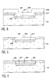
La description qui suit se réfère à la préparation d'un substrat à partir d'une plaque de silicium 10 d'un type de conductivité p. Les étapes peuvent être cependant transposées à une plaque de type n.The following description refers to the preparation of a substrate from a
Une couche d'oxyde de silicium 12, dite couche piédestal, est formée par oxydation à la surface de la plaque de silicium 10 et, sur cette couche 12, est formée une couche 14 de nitrure de silicium. La couche 14 de nitrure de silicium est mise en forme par une opération de masquage et de gravure de façon à mettre à nu la couche d'oxyde de silicium 12 dans certaines régions. Une oxydation localisée est alors réalisée dans ces régions pour former des pavés épais 16 d'oxyde de silicium. On obtient ainsi la structure représentée à la figure 1.A layer of
Les parties du substrat recouvertes par la couche 14 de nitrure de silicium sont désignées par première région et les parties occupées par les pavés d'oxyde de silicium 16, dont un seul est visible sur la figure 1, sont désignées par deuxièmes régions. Les première et deuxièmes régions sont repérées avec les références 20 et 22 respectivement.The parts of the substrate covered by the
Sur le substrat plusieurs "deuxièmes régions" 22 peuvent être formées. Elles sont alors entourées par la première région. Dans la suite du texte, il n'est cependant fait référence qu'à une seule deuxième région qui est celle visible sur les figures.On the substrate several "second regions" 22 can be formed. They are then surrounded by the first region. In the rest of the text, however, reference is made to only one second region which is that visible in the figures.
Une étape suivante du procédé consiste à éliminer la couche 14 de nitrure de silicium, les pavés 16 d'oxyde de silicium et la couche de piédestal 12, et former sur l'ensemble de la surface du substrat une fine couche d'oxyde de silicium 24. Cette couche est formée par oxydation. On obtient ainsi la structure de la figure 2.A next step in the process consists in eliminating the
Il apparaît sur la figure 2 qu'après cette étape la deuxième région 22 forme une dépression par rapport à la surface de la première région.It appears in Figure 2 that after this step the
La figure 3 illustre la formation d'une couche enterrée 26 d'oxyde de silicium. Pour former cette couche, des ions oxygène sont implantés dans la plaque de silicium 10 à travers sa surface. On peut noter à ce sujet que la couche d'oxyde de silicium 24 précédemment formée à la surface du substrat permet de décanaliser, c'est-à-dire contrôler avec précision le rayon de projection des ions oxygène implantés de façon à obtenir des zones implantées de concentration en oxygène homogènes.FIG. 3 illustrates the formation of a buried
Après l'implantation un recuit est effectué pour permettre de réaliser et de rendre cohérente la couche 26. La couche 26 délimite alors dans la plaquette de silicium 10 une couche superficielle de silicium 27, qu'elle isole électriquement d'une partie massive de silicium de la plaquette.After implantation, annealing is carried out to allow the
L'énergie et la dose des ions implantés sont choisies pour former la couche 26 à une profondeur donnée dans les première et deuxième régions 20, 22. A titre d'exemple, la couche 26 est enterrée à une profondeur comprise entre 10 nm et 200 nm Pour la réalisation d'une couche enterrée d'oxyde de silicium, on peut se reporter au document (2) dont la référence est indiquée à la fin de la présente description.The energy and the dose of the implanted ions are chosen to form the
La couche 26 suit le motif de dénivellation de la surface du substrat. Elle est en effet enterrée à une profondeur égale sous la surface du substrat dans les première et deuxième régions.
Les flèches 28 sur la figure 3 indiquent une orientation du faisceau d'implantation des ions oxygène. Elle forme un angle θ par rapport à la normale au plan du substrat. Ainsi, des ions sont également implantés dans le flanc de transition 30 entre les régions 20 et 22, au moins sur un côté de la deuxième région 22. Pour éviter le déficit d'ions par ombrage des plans, on procède à une rotation des plaquettes de façon à implanter la même dose sur tous les flancs.The
La dose d'ions implantée dans le flanc de transition 30 est égale à D.cosθ où D est la dose d'implantation dans les première et deuxième régions.The dose of ions implanted in the
L'angle d'implantation est choisi suffisamment faible, c'est-à-dire le profil d'oxydation est choisi suffisamment raide, pour que la couche 26, enterrée dans les régions 20, 22, affleure sensiblement à la surface du flanc de transition 30. On considère que la couche 26 affleure sensiblement à la surface lorsqu'elle est présente à la surface ou lorsqu'elle est proche de la surface, c'est-à-dire enterrée à une très faible profondeur.The implantation angle is chosen to be sufficiently small, that is to say the oxidation profile is chosen to be sufficiently stiff, so that the
Dans le cas où la couche enterrée 26 n'est pas présente à la surface du flanc 30, mais à une faible profondeur sous la surface, il est accessoirement possible d'effectuer une oxydation pour épaissir la couche d'oxyde de surface 24 jusqu'à ce que celle-ci atteigne la couche enterrée dans la région du flanc de transition 30.In the case where the buried
Une étape suivante consiste à effectuer une désoxydation partielle permettant d'éliminer complètement la couche d'oxyde 24 à la surface du substrat et d'éliminer l'oxyde des couches 24 et 26 sur le flanc de transition 30. La couche 27 de silicium, et le silicium de la plaquette 10, sur le flanc 30 sont ainsi mis à nu.A next step consists in carrying out a partial deoxidation making it possible to completely eliminate the
La structure montrée à la figure 4 est obtenue en formant sur le silicium mis à nu une couche de silicium monocristallin 32. Cette couche est formée par épitaxie, préférentiellement à une température comprise entre 850°C et 1300°C, par exemple à 1100°C.The structure shown in Figure 4 is obtained by forming on the exposed silicon a layer of
L'épitaxie est contrôlée à partir de la couche superficielle 27 dans les première et deuxième régions 20, 22, et du silicium sur le flanc 30.The epitaxy is controlled from the
De façon avantageuse, l'épitaxie de la couche monocristalline 32 peut être précédée d'un recuit pour éliminer toute contamination résiduelle et pour réduire au minimum les défauts dans la couche de silicium 27.Advantageously, the epitaxy of the
Une étape suivante consiste à aplanir la couche de silicium avec arrêt sur la couche 26 de la première région 20. L'aplanissement est effectué, par exemple, par un polissage mécanochimique. On obtient la structure représentée à la figure 5.A next step consists in flattening the silicon layer with a stop on the
La couche "enterrée" 26 de la première région 20 est mise à nu et apparaît désormais à la surface du substrat. Dans la deuxième région 22, la couche 26 d'oxyde de silicium reste recouverte par la couche 27 de silicium et par la couche 32 de silicium monocristallin dont l'épaisseur a été réduite au cours de l'aplanissement. La surface du substrat dans les première et deuxième régions se trouve dans un même plan après cette étape.The "buried"
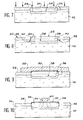
Une étape suivante consiste en une oxydation de la surface du substrat, comme le montre la figure 6. Cette étape permet, en formant une nouvelle couche d'oxyde de silicium 34, d'épaissir la couche 26 d'oxyde de silicium dans la première région 30 et d'amincir la couche de silicium 32 dans la deuxième région 22.A next step consists of an oxidation of the surface of the substrate, as shown in FIG. 6. This step makes it possible, by forming a new layer of
Une implantation d'impuretés dopantes conduisant à un dopage de même type de conductivité que la plaquette de substrat 10, est effectuée à travers la couche 34. Il s'agit en l'occurrence d'impuretés de bore, conduisant à un dopage de type p.Implantation of doping impurities leading to doping of the same type of conductivity as the
L'implantation, matérialisée par des flèches sur la figure 7, permet de former une zone dopée 36 de type p+ qui s'étend sous la couche 26 d'oxyde de silicium dans la première région 20 et au-dessus de la couche 26, dans la deuxième région 22. Dans la deuxième région 22, la zone dopée correspond à la couche 27 et à une partie au moins de la couche 32.The implantation, shown by arrows in FIG. 7, makes it possible to form a doped
La zone dopée 36 qui passe dans la région du flanc de transition 30 entre les régions 20 et 22 permet d'améliorer une prise de contact électrique entre la partie de la deuxième région située au-dessus de la couche d'oxyde de silicium 26, et désignée par la suite par région "active" 38 et la partie massive de la plaquette de silicium 10.The doped
La zone 36 a aussi un rôle d'anti-perçage dans la région active 38 où sont formés par la suite les transistors.The
Une désoxydation partielle suit l'implantation de bore. Elle permet de découvrir la partie active 38 dont la couche 32 a été amincie, tout en préservant une partie, également amincie, de la couche 26 d'oxyde de silicium dans la première région. On obtient la structure représentée à la figure 8.Partial deoxidation follows the implantation of boron. It allows the
Lorsque la formation de la couche d'oxyde de silicium est réalisée à une température assez élevée, de l'ordre de 1050°C, on obtient au terme de la désoxydation un bord arrondi entre la partie active 38 et la couche d'oxyde de silicium 26. Ce bord arrondi est repéré avec la référence 40.When the formation of the silicon oxide layer is carried out at a fairly high temperature, of the order of 1050 ° C., at the end of the deoxidation, a rounded edge is obtained between the
Le substrat finalement obtenu comporte une série de caissons avec une structure de type SOI, il s'agit des deuxièmes régions, et isolés mutuellement à la surface par la couche d'oxyde de silicium de la première région.The substrate finally obtained comprises a series of wells with an SOI type structure, these are the second regions, and mutually isolated at the surface by the layer of silicon oxide from the first region.
Une ou plusieurs prises de contact formées à travers les flancs des caissons conformément au procédé décrit ci-dessus, permettent d'évacuer les charges (trous) accumulées dans les régions actives vers la partie massive du substrat et éviter ainsi l'effet kink. Sur la figure 8, les prises de contact sont repérées avec la référence 39.One or more contact points formed through the sides of the boxes in accordance with the method described above, make it possible to evacuate the charges (holes) accumulated in the active regions towards the massive part of the substrate and thus avoid the kink effect. In FIG. 8, the contacts are identified with the
Les figures 9 et 10 illustrent une utilisation du substrat préparé de la façon décrite ci-dessus pour la réalisation d'un transistor à effet de champ. Les étapes de fabrication de ce transistor sont décrites sommairement ci-dessous.FIGS. 9 and 10 illustrate a use of the substrate prepared as described above for the production of a field effect transistor. The manufacturing steps for this transistor are briefly described below.
La figure 9 montre la formation, notamment à la surface de la région active, d'une couche d'oxyde de grille 50 (SiO2) et le dépôt d'une couche de matériau de grille 52, par exemple de silicium polycristallin.FIG. 9 shows the formation, in particular at the surface of the active region, of a layer of gate oxide 50 (SiO 2 ) and the deposition of a layer of
La couche 52 est ensuite mise en forme par formation d'un masque (non représenté) et par gravure sélective, pour obtenir une grille 54 représentée à la figure 10.The
Des régions de source 56 et de drain 58 sont réalisées dans la région active par implantation, en utilisant la grille 54 comme masque.
Les régions 56 et 58 sont de préférence réalisés par une double implantation, par exemple avec des ions conduisant à une conductivité de type opposée à celle de la plaquette massive de silicium du substrat, c'est-à-dire opposée à celle de la région active.The
Une première implantation avec une dose légère est suivie par la formation d'espaceurs latéraux 60 sur la grille 54 et par une deuxième implantation à plus forte dose.A first implantation with a light dose is followed by the formation of
Dans le cas illustré, une implantation d'ions conduisant à une conductivité de type n permet de former un transistor à canal n.In the illustrated case, an implantation of ions leading to an n-type conductivity makes it possible to form an n-channel transistor.
Le transistor ou les circuits ainsi réalisés ne présentent pas de base parasite à potentiel flottant. Ceci permet de les affranchir de l'effet kink et par conséquent de polariser le transistor avec des tensions supérieures à celles généralement admises pour les dispositifs MOS sur des substrats de type SOI.The transistor or the circuits thus produced do not have a parasitic base with floating potential. This makes it possible to free them from the kink effect and therefore to bias the transistor with voltages higher than those generally accepted for MOS devices on SOI type substrates.
Cette propriété procure notamment l'avantage de pouvoir augmenter les performances des transistors ainsi réalisés.This property provides in particular the advantage of being able to increase the performance of the transistors thus produced.
-
(1)
"Analysis of Kink Characteristics in Silicon-on-Insulator MOSFET's Using Two-Carrier Modeling de KOICHI KATO et al., IEEE Transaction on electron devices vol. E.D. 32, n° 2, February 1985, pp. 458-462 (1)
"Analysis of Kink Characteristics in Silicon-on-Insulator MOSFET's Using Two-Carrier Modeling by KOICHI KATO et al., IEEE Transaction on electron devices vol.ED 32, n ° 2, February 1985, pp. 458-462 -
(2)
Microstructures of silicon implanted with high dose oxygen ions de C. Jaussaud et al. Appl. Phys. Lett. 46(11), 1 dune 1985, pp. 1064-1066. (2)
Microstructures of silicon implanted with high dose oxygen ions by C. Jaussaud et al. Appl. Phys. Lett. 46 (11), 1 dune 1985, pp. 1064-1066.
Claims (11)
Applications Claiming Priority (2)
| Application Number | Priority Date | Filing Date | Title |
|---|---|---|---|
| FR9603448A FR2746544B1 (en) | 1996-03-20 | 1996-03-20 | SILICON TYPE SUBSTRATE ON INSULATION FOR THE MANUFACTURE OF TRANSISTORS AND PROCESS FOR PREPARING SUCH SUBSTRATE |
| FR9603448 | 1996-03-20 |
Publications (3)
| Publication Number | Publication Date |
|---|---|
| EP0797252A2 true EP0797252A2 (en) | 1997-09-24 |
| EP0797252A3 EP0797252A3 (en) | 1997-11-26 |
| EP0797252B1 EP0797252B1 (en) | 2008-05-21 |
Family
ID=9490343
Family Applications (1)
| Application Number | Title | Priority Date | Filing Date |
|---|---|---|---|
| EP97400602A Expired - Lifetime EP0797252B1 (en) | 1996-03-20 | 1997-03-18 | Silicon on insulator substrate for fabricating transistors and method for preparing such a substrate |
Country Status (7)
| Country | Link |
|---|---|
| US (1) | US5897939A (en) |
| EP (1) | EP0797252B1 (en) |
| JP (1) | JP4065580B2 (en) |
| KR (1) | KR970067611A (en) |
| CA (1) | CA2200264A1 (en) |
| DE (1) | DE69738700D1 (en) |
| FR (1) | FR2746544B1 (en) |
Cited By (3)
| Publication number | Priority date | Publication date | Assignee | Title |
|---|---|---|---|---|
| EP0959497A1 (en) * | 1998-05-20 | 1999-11-24 | Sharp Kabushiki Kaisha | A method of forming an ultra-thin soi electrostatic discharge protection device |
| GB2352876A (en) * | 1996-03-01 | 2001-02-07 | Sven E Wahlstrom | Recessed gate transistor with overlying silicon on insulator straucture |
| US6413830B1 (en) | 1996-03-01 | 2002-07-02 | Sven E. Wahlstrom | Dynamic random access memory |
Families Citing this family (9)
| Publication number | Priority date | Publication date | Assignee | Title |
|---|---|---|---|---|
| US6331181B1 (en) * | 1998-12-08 | 2001-12-18 | Intuitive Surgical, Inc. | Surgical robotic tools, data architecture, and use |
| US6956268B2 (en) * | 2001-05-18 | 2005-10-18 | Reveo, Inc. | MEMS and method of manufacturing MEMS |
| US7045878B2 (en) * | 2001-05-18 | 2006-05-16 | Reveo, Inc. | Selectively bonded thin film layer and substrate layer for processing of useful devices |
| US7033910B2 (en) * | 2001-09-12 | 2006-04-25 | Reveo, Inc. | Method of fabricating multi layer MEMS and microfluidic devices |
| US20090065471A1 (en) * | 2003-02-10 | 2009-03-12 | Faris Sadeg M | Micro-nozzle, nano-nozzle, manufacturing methods therefor, applications therefor |
| US6875671B2 (en) * | 2001-09-12 | 2005-04-05 | Reveo, Inc. | Method of fabricating vertical integrated circuits |
| US7163826B2 (en) * | 2001-09-12 | 2007-01-16 | Reveo, Inc | Method of fabricating multi layer devices on buried oxide layer substrates |
| KR100673133B1 (en) * | 2006-01-23 | 2007-01-22 | 주식회사 하이닉스반도체 | Method for fabricating semiconductor device |
| CN111129054B (en) * | 2019-12-23 | 2023-09-05 | 上海集成电路研发中心有限公司 | CMOS image sensor structure and manufacturing method |
Citations (3)
| Publication number | Priority date | Publication date | Assignee | Title |
|---|---|---|---|---|
| US4968636A (en) * | 1988-09-14 | 1990-11-06 | Oki Electric Industry Co., Ltd. | Embedded isolation region and process for forming the same on silicon substrate |
| US4997786A (en) * | 1986-06-13 | 1991-03-05 | Matsushita Electric Industrial Co., Ltd. | Method of fabricating a semiconductor device having buried insulation layer separated by ditches |
| EP0540277A2 (en) * | 1991-10-31 | 1993-05-05 | STMicroelectronics, Inc. | Method for planarized isolation for CMOS devices |
Family Cites Families (2)
| Publication number | Priority date | Publication date | Assignee | Title |
|---|---|---|---|---|
| FR2563377B1 (en) * | 1984-04-19 | 1987-01-23 | Commissariat Energie Atomique | METHOD FOR MANUFACTURING AN INSULATING LAYER BURIED IN A SEMICONDUCTOR SUBSTRATE, BY ION IMPLANTATION |
| US4601779A (en) * | 1985-06-24 | 1986-07-22 | International Business Machines Corporation | Method of producing a thin silicon-on-insulator layer |
-
1996
- 1996-03-20 FR FR9603448A patent/FR2746544B1/en not_active Expired - Fee Related
-
1997
- 1997-02-25 US US08/806,066 patent/US5897939A/en not_active Expired - Lifetime
- 1997-03-18 DE DE69738700T patent/DE69738700D1/en not_active Expired - Lifetime
- 1997-03-18 EP EP97400602A patent/EP0797252B1/en not_active Expired - Lifetime
- 1997-03-18 CA CA002200264A patent/CA2200264A1/en not_active Abandoned
- 1997-03-19 JP JP06676897A patent/JP4065580B2/en not_active Expired - Fee Related
- 1997-03-20 KR KR1019970009424A patent/KR970067611A/en not_active Application Discontinuation
Patent Citations (3)
| Publication number | Priority date | Publication date | Assignee | Title |
|---|---|---|---|---|
| US4997786A (en) * | 1986-06-13 | 1991-03-05 | Matsushita Electric Industrial Co., Ltd. | Method of fabricating a semiconductor device having buried insulation layer separated by ditches |
| US4968636A (en) * | 1988-09-14 | 1990-11-06 | Oki Electric Industry Co., Ltd. | Embedded isolation region and process for forming the same on silicon substrate |
| EP0540277A2 (en) * | 1991-10-31 | 1993-05-05 | STMicroelectronics, Inc. | Method for planarized isolation for CMOS devices |
Non-Patent Citations (2)
| Title |
|---|
| IBM TECHNICAL DISCLOSURE BULLETIN, vol. 31, no. 8, 1 Janvier 1989, page 114/115 XP000104754 "SELF-ALIGNED QUASI-SEMICONDUCTOR-ON-INSULATOR CMOS STRUCTURE" * |
| NUCLEAR INSTRUMENTS & METHODS IN PHYSICS RESEARCH, SECTION - B: BEAM INTERACTIONS WITH MATERIALS AND ATOMS, vol. B55, no. 1 / 04, 2 Avril 1991, pages 856-859, XP000230740 BUSSMANN U ET AL: "OXYGEN IMPLANTATION THROUGH PATTERNED MASKS: A METHOD FOR FORMING INSULATED SILICON DEVICE ISLANDS WHILE MAINTAINING A PLANAR WAFER SURFACE" * |
Cited By (9)
| Publication number | Priority date | Publication date | Assignee | Title |
|---|---|---|---|---|
| GB2352876A (en) * | 1996-03-01 | 2001-02-07 | Sven E Wahlstrom | Recessed gate transistor with overlying silicon on insulator straucture |
| GB2352877A (en) * | 1996-03-01 | 2001-02-07 | Sven E Wahlstrom | Silicon on insulator DRAM trench capacitor |
| GB2352878A (en) * | 1996-03-01 | 2001-02-07 | Sven E Wahlstrom | Formation of a capacitor in a semiconductor substrate |
| GB2352878B (en) * | 1996-03-01 | 2001-03-21 | Sven E Wahlstrom | Dynamic random access memory |
| GB2352876B (en) * | 1996-03-01 | 2001-03-21 | Sven E Wahlstrom | Dynamic random access memory |
| GB2352877B (en) * | 1996-03-01 | 2001-03-21 | Sven E Wahlstrom | Dynamic random access memory |
| US6413830B1 (en) | 1996-03-01 | 2002-07-02 | Sven E. Wahlstrom | Dynamic random access memory |
| EP0959497A1 (en) * | 1998-05-20 | 1999-11-24 | Sharp Kabushiki Kaisha | A method of forming an ultra-thin soi electrostatic discharge protection device |
| US6080612A (en) * | 1998-05-20 | 2000-06-27 | Sharp Laboratories Of America, Inc. | Method of forming an ultra-thin SOI electrostatic discharge protection device |
Also Published As
| Publication number | Publication date |
|---|---|
| US5897939A (en) | 1999-04-27 |
| DE69738700D1 (en) | 2008-07-03 |
| FR2746544A1 (en) | 1997-09-26 |
| FR2746544B1 (en) | 1998-05-15 |
| JP4065580B2 (en) | 2008-03-26 |
| KR970067611A (en) | 1997-10-13 |
| EP0797252B1 (en) | 2008-05-21 |
| JPH1022398A (en) | 1998-01-23 |
| CA2200264A1 (en) | 1997-09-20 |
| EP0797252A3 (en) | 1997-11-26 |
Similar Documents
| Publication | Publication Date | Title |
|---|---|---|
| EP0298794B1 (en) | Process for making a buried insulating layer in a semiconductor substrate by ion implantation and semiconductor structure comprising such a layer | |
| EP1145300B1 (en) | Method of manufacturing a mis transistor on a semiconductor substrate | |
| EP1266409B1 (en) | Mos transistor with metal source and drain, and method for manufacturing the same | |
| EP0462882A1 (en) | Thin film field effect transistor with buried gate and its method of fabrication | |
| EP0797252B1 (en) | Silicon on insulator substrate for fabricating transistors and method for preparing such a substrate | |
| FR2899017A1 (en) | METHOD FOR MAKING A CHANNEL TRANSISTOR COMPRISING GERMANIUM | |
| FR2823009A1 (en) | Vertical transistor production with insulated gate with weak overlapping of gate on source and drain comprises forming vertical semiconductor column by anisotropic engraving and formation of insulated dielectric gate | |
| FR2972567A1 (en) | METHOD OF FORMING A STRUCTURE OF GE ON III / V ON INSULATION | |
| FR2795554A1 (en) | Making silicon-on-nothing architecture for high-speed CMOS signal- and low voltage power devices, includes formation of internal passivated or insulated cavities in stacked semiconductor assemblies | |
| EP3531444A1 (en) | Integrated circuit including a substrate provided with a region rich in traps, and method for manufacturing same | |
| FR3042907A1 (en) | METHOD FOR MANUFACTURING A MOS TRANSISTOR DEVICE | |
| WO2015150257A1 (en) | Method for manufacture of a semiconductor wafer suitable for the manufacture of an soi substrate, and soi substrate wafer thus obtained | |
| FR2708142A1 (en) | Method of manufacturing a transistor in silicon on insulator technology. | |
| FR2806833A1 (en) | Fabrication of MOS transistor having two gates, one being buried, includes forming semiconductor channel region transversely mounting a first gate, and forming second gate on channel region | |
| EP1483793A2 (en) | Schottky power diode comprising a sicoi substrate and the method of producing one such diode | |
| EP4088312B1 (en) | Method for manufacturing a semiconductor-on-insulator structure for radiofrequency applications | |
| WO2020136343A1 (en) | Semiconductor structure for digital and radiofrequency applications | |
| FR3076397A1 (en) | PROCESS FOR PRODUCING A TRANSISTOR | |
| EP3903342B1 (en) | Semiconductor structure for digital and radiofrequency applications, and method for manufacturing such a structure | |
| FR3035265A1 (en) | METHOD FOR MANUFACTURING SOI TRANSISTORS FOR INCREASED INTEGRATION DENSITY | |
| EP1407486A2 (en) | Transistor and method for making a transistor on a sige/soi substrate | |
| FR2691289A1 (en) | Field effect semiconductor device, method of making and applying to a matrix-controlled device | |
| FR3136109A1 (en) | Silicon-on-insulator type semiconductor device and corresponding manufacturing method | |
| EP0577497A1 (en) | Vertical JFET transistor with low gate/substrate capacity and process for making the same |
Legal Events
| Date | Code | Title | Description |
|---|---|---|---|
| PUAI | Public reference made under article 153(3) epc to a published international application that has entered the european phase |
Free format text: ORIGINAL CODE: 0009012 |
|
| AK | Designated contracting states |
Kind code of ref document: A2 Designated state(s): DE GB IT NL |
|
| PUAL | Search report despatched |
Free format text: ORIGINAL CODE: 0009013 |
|
| RHK1 | Main classification (correction) |
Ipc: H01L 21/762 |
|
| AK | Designated contracting states |
Kind code of ref document: A3 Designated state(s): DE GB IT NL |
|
| 17P | Request for examination filed |
Effective date: 19980509 |
|
| RAP1 | Party data changed (applicant data changed or rights of an application transferred) |
Owner name: COMMISSARIAT A L'ENERGIE ATOMIQUE |
|
| GRAP | Despatch of communication of intention to grant a patent |
Free format text: ORIGINAL CODE: EPIDOSNIGR1 |
|
| GRAS | Grant fee paid |
Free format text: ORIGINAL CODE: EPIDOSNIGR3 |
|
| GRAA | (expected) grant |
Free format text: ORIGINAL CODE: 0009210 |
|
| AK | Designated contracting states |
Kind code of ref document: B1 Designated state(s): DE GB IT NL |
|
| REG | Reference to a national code |
Ref country code: GB Ref legal event code: FG4D Free format text: NOT ENGLISH |
|
| REF | Corresponds to: |
Ref document number: 69738700 Country of ref document: DE Date of ref document: 20080703 Kind code of ref document: P |
|
| NLV1 | Nl: lapsed or annulled due to failure to fulfill the requirements of art. 29p and 29m of the patents act | ||
| PG25 | Lapsed in a contracting state [announced via postgrant information from national office to epo] |
Ref country code: NL Free format text: LAPSE BECAUSE OF FAILURE TO SUBMIT A TRANSLATION OF THE DESCRIPTION OR TO PAY THE FEE WITHIN THE PRESCRIBED TIME-LIMIT Effective date: 20080521 |
|
| PLBE | No opposition filed within time limit |
Free format text: ORIGINAL CODE: 0009261 |
|
| STAA | Information on the status of an ep patent application or granted ep patent |
Free format text: STATUS: NO OPPOSITION FILED WITHIN TIME LIMIT |
|
| 26N | No opposition filed |
Effective date: 20090224 |
|
| PGFP | Annual fee paid to national office [announced via postgrant information from national office to epo] |
Ref country code: IT Payment date: 20110324 Year of fee payment: 15 |
|
| PGFP | Annual fee paid to national office [announced via postgrant information from national office to epo] |
Ref country code: GB Payment date: 20110321 Year of fee payment: 15 Ref country code: DE Payment date: 20110325 Year of fee payment: 15 |
|
| GBPC | Gb: european patent ceased through non-payment of renewal fee |
Effective date: 20120318 |
|
| PG25 | Lapsed in a contracting state [announced via postgrant information from national office to epo] |
Ref country code: GB Free format text: LAPSE BECAUSE OF NON-PAYMENT OF DUE FEES Effective date: 20120318 |
|
| REG | Reference to a national code |
Ref country code: DE Ref legal event code: R119 Ref document number: 69738700 Country of ref document: DE Effective date: 20121002 |
|
| PG25 | Lapsed in a contracting state [announced via postgrant information from national office to epo] |
Ref country code: IT Free format text: LAPSE BECAUSE OF NON-PAYMENT OF DUE FEES Effective date: 20120318 |
|
| PG25 | Lapsed in a contracting state [announced via postgrant information from national office to epo] |
Ref country code: DE Free format text: LAPSE BECAUSE OF NON-PAYMENT OF DUE FEES Effective date: 20121002 |